Abstract
Power losses of switches and inductors are consistent challenges that hinder the development of high-frequency power supply in package (PSiP). This paper investigates the roadmap for power loss optimizations of switches and inductors in high-frequency PSiPs. Firstly, a size and parallel quantity design method to reduce power loss in an integrated Si LDMOSFET is provided with comprehensive consideration of switching frequency and power levels. Secondly, quality factors of different air-core inductors are analyzed with consideration of geometric parameters and skin effect, which provides the winding structure optimization to reduce power losses. The power losses of the integrated Si LDMOSFET and air-core inductors are both reduced to less than 10% of the output power at 1~100 MHz switching frequency and 0.1~10 W power level. Finally, based on the above optimizations, power losses of switches and inductors are calculated with switching frequency and power level. Combining the calculated results, this paper predicts the efficiency boundaries of PSiPs. Upon efficiency normalization with consideration of input and output voltage levels, all the predictions are consistent with the published literature. The efficiency predication error is 1~15% at 1~100 MHz switching frequency and 0.1~10 W power level. The above power loss optimizations improve the efficiency, which provides potential roadmaps for achieving high-frequency PSiPs.
1. Introduction
In CPU and MCU applications, there is a consistent pursuit of high-frequency point-of-load (PoL) power supplies [1,2,3]. The switching frequency has been increasing in the past few decades [4]. This miniaturizes switches and inductors that primarily dominate the system size and weight. As a result, the integration level has evolved into a 3D stacked power supply (3D-SPS, discrete switch and discrete inductor), power supply in package (PSiP, integrated switch and discrete inductor), and power supply on chip (PwrSoC, integrated switch and integrated inductor) [5,6,7]. These integration levels differentiate in switching frequency and power rate and applications, as shown in Table 1.

Table 1.
Switching Frequencies and Power Levels of Different Integration Levels.
The 3D-SPS adopts discrete switches and inductors, which allows for high power conversion (up to 100 W) [8,9,10]. It carries out a 3D stacking structure on the PCB, and usually places magnetic components above or below the entire PCB board. With relative high inductance, the 3D-SPS approach can operate at a switching frequency below 10 MHz. The reduced switching frequency benefits the overall efficiency, since the switching loss is proportional to the switching frequency.
The PSiP integrates all components in one package, which achieves single chip power conversion [7,11]. Typically, it integrates power switches, drivers and control modules on a single die, whereas discrete inductors with low profile are packaged into the chip. Owing to the reduced inductance, the PSiP approach usually operates at a frequency above 10 MHz that leads to high switching loss and reduced efficiency. Due to limited power devices and heat dissipation, the power range is restricted to under 10 W.
The PwrSoC integrates all components on a single die, which achieves the highest integration level [12,13,14]. The integrated on-chip power supply can be placed as near to the load as possible, which reduces the transmission loss in power lines [15]. However, with a low on-chip inductance, the switching frequency usually increases above 100 MHz to reduce ripples. As a result, power loss and heat dissipation are hard to optimize and that limits the power rate to below 2 W.
In comparison to 3D-SPS, the PSiP saves the interconnecting area of the control chip, which drives chip and power transistors in 3D-SPS. In comparison to PwrSoC, the PSiP generally adopts the standard CMOS process and does not require the CMOS process with power inductors, which is more mature and compatible with technology. Therefore, the PSiP power supply is more widely applied in communication, server automatic systems and so on.
For all integration levels, switching frequency and power levels are usually contradictory, and the major challenges toward high frequency are power losses of switches and inductors, as shown in Figure 1.
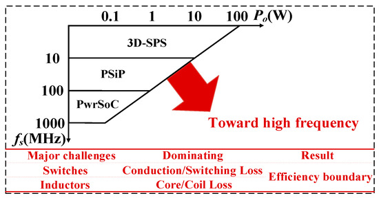
Figure 1.
Roadmap for high-frequency PoL power supplies.
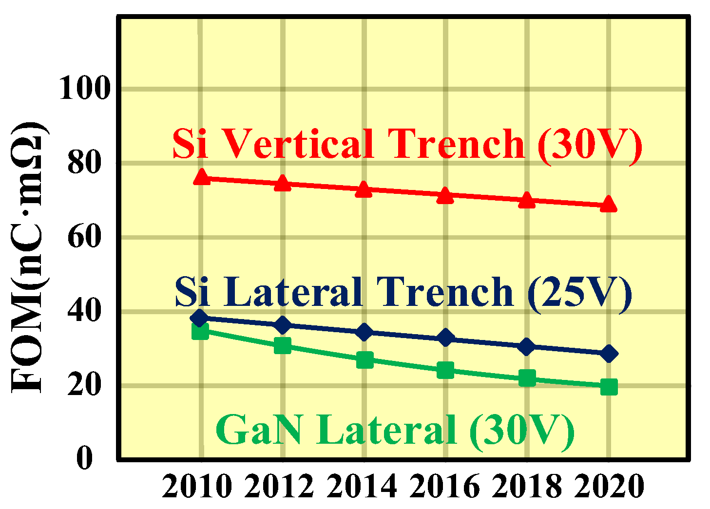
Among the major challenges, the power switch dominates conduction and switching losses. Conduction and switching losses are primarily determined by the on-resistance value (Ron) and total gate charge value (QG), respectively. Figure-of-merits (FOM = Ron × QG) of the Si vertical trench, Si lateral trench and GaN lateral trench are shown in Figure 2 [16,17,18]. Due to the wider bandgap, higher electron mobility and electron velocity of GaN HEMT, its FOM is several times lower than that of Si MOSFET. These material characteristics result in lower power losses in GaN HEMT in high-frequency applications. However, GaN HEMTs are usually discretely packaged due to unique fabrication processes, which are preferable in 3D-SPS [19,20,21]. For low-power and high-integrated applications, the Si lateral diffused MOSFET (LDMOSFET) is usually applied in PSiP and PwrSoC because of compatible fabrication processes [22].

Figure 2.
FOMs of GaN HEMT and Si MOSFET.
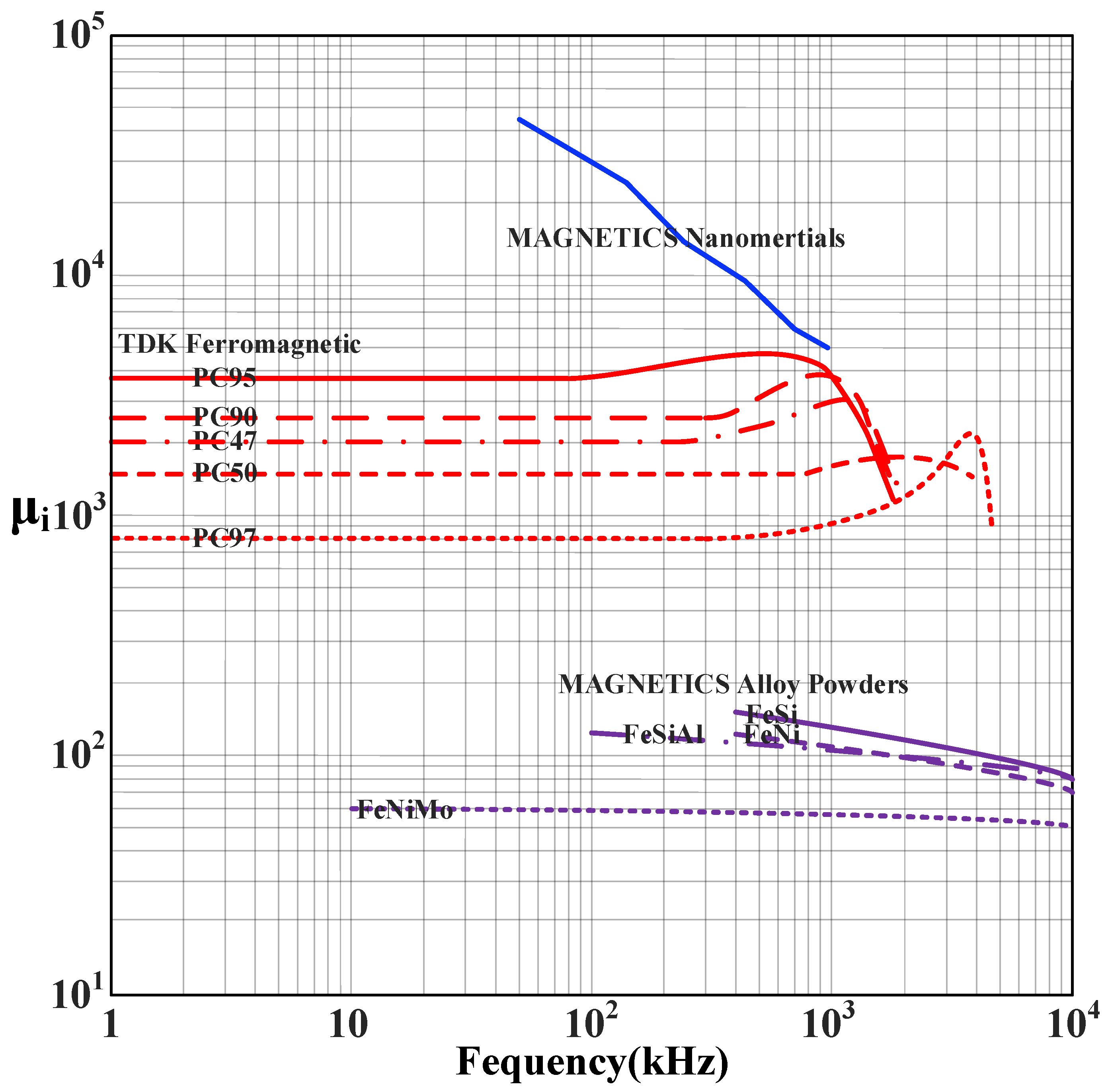
The power inductor dominates core and coil losses and primarily determines integration levels. Although the magnetic core helps increase the inductance, the core loss increases rapidly with frequency that harms the efficiency. For magnetic cores, their magnetic permeability, μi, of soft magnetic material decreases dramatically when the operating frequency reaches a critical value, which causes the dramatic decrement of the inductance value. In TDK Mn-Zn ferrites, MAGNETICS nanomaterial and alloy powders, their initial relative magnetic permeability, μi, is shown in Figure 3 [23,24,25]. Figure 3 shows that the permeability of magnetic materials decreases rapidly above 1 MHz. As the switching frequency increases, high-frequency inductors evolve from magnetic-core inductors to air-core inductors [26,27,28]. Without magnetic cores, air-core inductors do not suffer core loss and have good linearity to frequency. The inductance value decreases dramatically due to the removal of the magnetic core. In the literature and products, the typical inductance values of solenoid and planar spiral inductors are given in Table 2. All the investigated inductance values are less than 500 nH, which pushes the PoL power supply to operate at a frequency above 1 MHz.

Figure 3.
Initial relative magnetic permeabilities of TDK Mn-Zn ferrites, MAGNETICS nanomaterial and alloy powders.
Table 2.
Typical Inductance Values of Solenoid and Planar Spiral Inductors.
To address the above challenges, this paper analyzes integrated Si LDMOSFTs and air-core inductors in PSiPs. In terms of the integrated Si LDMOSFET, with consideration of parasitic resistors and capacitors, the size and parallel quantity optimization of integrated Si LDMOSFET are provided to reduce the switching and conduction losses. In terms of air-core inductors, with consideration of skin effect, quality factors of various air-core inductors are calculated for the winding structure optimization to reduce coil loss. Furthermore, combining the above optimizations, this paper predicts the efficiency boundaries of PSiP approaches based on power losses of switches and inductors.
This paper is organized as follows. Section 2 analyzes power losses of an integrated Si LDMOSFET to provide a size and parallel quantity optimization. Section 3 calculates the quality factors of solenoid inductors and planar spiral inductors to optimize winding structures. Section 4 predicts the efficiency boundaries of PSiP. Section 5 concludes this paper.
2. Power Loss Analysis of Integrated Si LDMOSFET
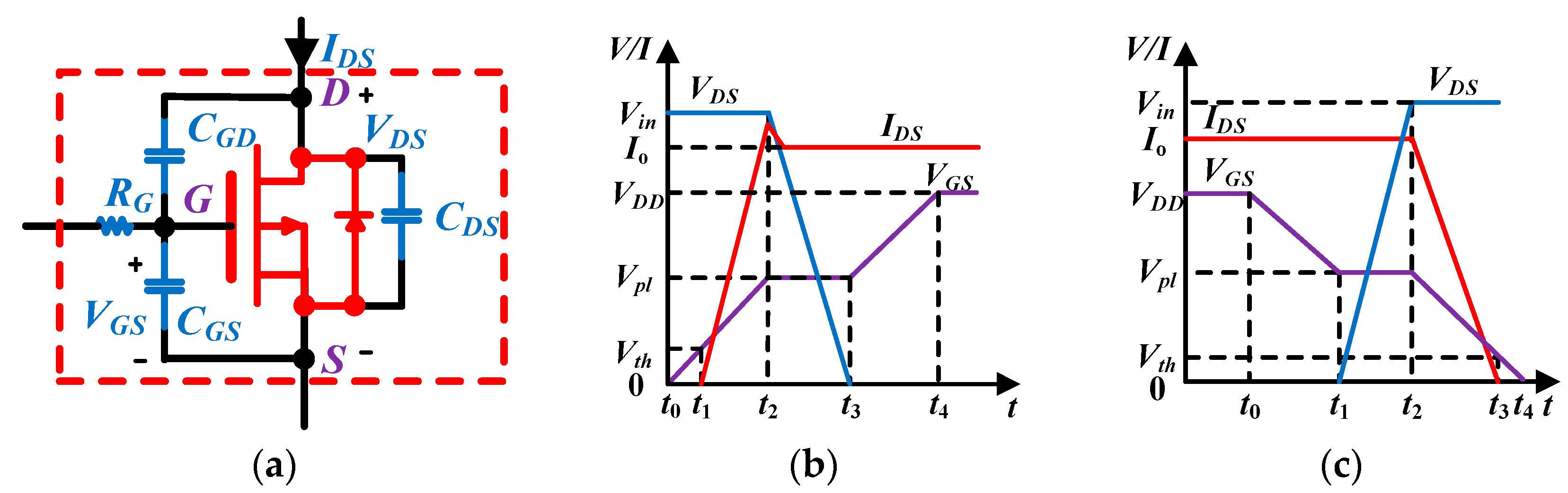
In PSiPs, integrated Si MOSFETs have the most severe heat dissipation and the easiest thermal breakdown of all power devices. For PSiP, power loss caused by high frequency is a great challenge in terms of designing power switches. Power losses of integrated Si LDMOSFETs mainly include switching loss, driving loss, conduction loss and other power losses [35,36]. The equivalent model and switching process of an integrated Si LDMOSFET is shown in Figure 4. In Figure 4b,c, the gate voltage VGS exits the miller platform due to the inductor in the output filter.

Figure 4.
Equivalent model and switching process of an integrated Si LDMOSFET: (a) equivalent model (b) turn-on process (c) turn-off process.
Switching loss: At the period t1~t3 in turn-on and turn-off processes, the triangular overlapping area of drain-source current and voltage are switching losses. Therefore, according to the overlapping area, the switching loss is given by
Driving loss: At the period t0~t5 in turn-on and turn-off processes, gate voltage, VGS, rises or falls via the charge, CGS, or discharge, CGD. The stored energies of CGS and CGD are dissipated by the driving resistor, RG, which depends on the gate charge, QG. The driving loss is given by
Conduction loss: In on-state, the Si LDMOSFET is equivalent to the on-resistor, Ron, dissipating the energy. Conduction loss is given by
Other power losses: Other power losses mainly include output capacitance power loss and body diode power loss. The output capacitor stores the energy in off-state and releases the energy via the conducting channel in on-state. Based on the stored and released energies in a switching cycle, the output capacitance power loss is given by
The body diode power loss includes forward conduction loss and reverse recovery loss. The forward conduction loss is caused by the forward body diode current during the dead time. It is given by
where VF and td are the forward conduction voltage and forward conduction time of the body diode.
The reverse recovery loss is caused by the body diode reverse recovery after carrying the forward current. It is expressed as
where VDR and Qrr are the reverse recovery voltage and reverse recovery charge of the body diode.
Combining (1)–(6), the total power loss of M switches in parallel is given as
where X1, X2, X3, X4, X5 and X6 represent coefficients in total power loss that do not depend on switching frequency and output current.
Based on the capacitance value per unit length and area, CISS, COSS and CRSS of the integrated Si LDMOSFET are given by [37]
Based on I–V characteristic of the integrated Si LDMOSFET in the deep linear area, the on-resistance value is given by
Based on (8) and (9), (7) can be derived as
where coefficients Y1, Y2, Y3 and Y4 are obtained from X1, X2, X3, X5 and X6 by excluding the channel width, WM.
In (10), the power loss of the switch is determined by switching frequency, fs, output current, Io, switch size, WM, and parallel quantity, M. As usual, fs and Io are determined by the power supply requirements. In order to reduce power loss, WM and M are optimized as follows.
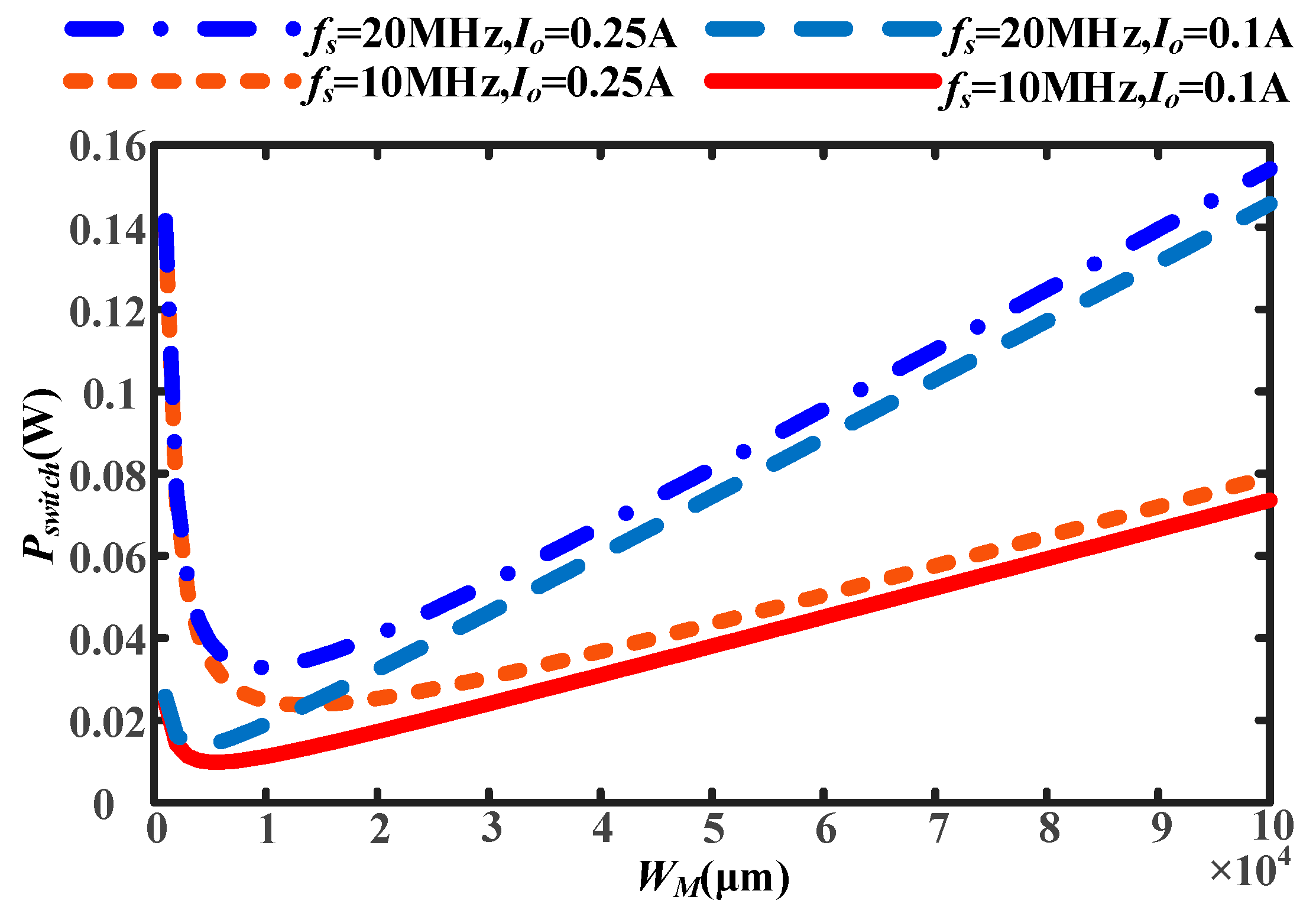
- M = 1: According to (10), taking Vin = 5 V and the 350 nm process as an example, the power loss is plotted with the integrated Si LDMOSFET size in Figure 5. It is obvious that there are different optimal sizes to minimize power loss at different switching frequencies and output currents [38]. This optimal size can be obtained by the simulation scan.
 Figure 5. Power loss of the integrated Si LDMOSFET with size WM when M = 1.
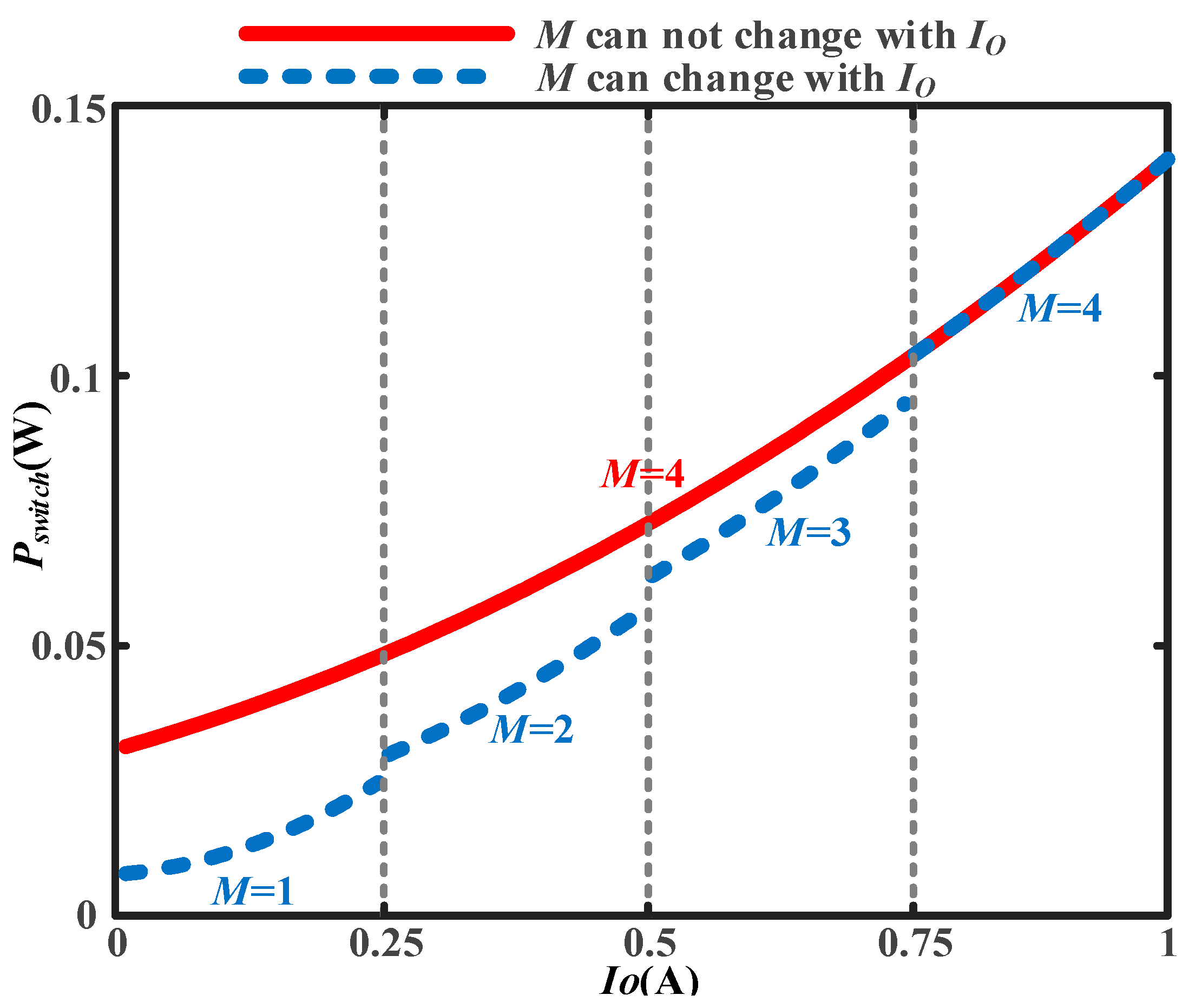
 - M ≠ 1: In fact, switch size is limited by the process. Therefore, the power switch is composed of multiple units in parallel. According to (10), the power loss is plotted with the output current in Figure 6. The size of a single unit is optimized at fs = 10 MHz and Io = 0.25 A, according to Figure 5. In Figure 6, comparing M = 4 to all load current ranges, the parallel quantity of power switch changing with drain-source current is more beneficial to improving overall efficiency [39].
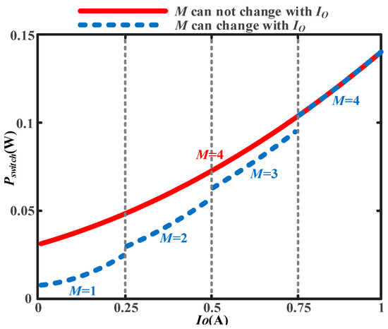 Figure 6. Power loss of the integrated Si LDMOSFET with drain-source current when M ≠ 1.
3. Quality Factor Analysis of Air-Core Inductors
In PSiPs, the power loss of air-core inductors can be increased due to high-frequency effects. For megahertz PoL applications, power losses of air-core inductors are related to the inductance current, geometric parameters of coil-wire, coil material, skin effect, eddy effect, proximity effect, fringe effect, etc. Among many factors, the geometric parameters and skin effect are highly related to the switching frequency. To calculate the power loss of the air-core inductors, the inductance current is expanded into sinusoidal waves of various frequencies. Their frequencies and amplitudes are fs, 2fs, 3fs, … and IL1, IL2, IL3, … respectively. Upon consideration of the geometric parameters and skin effect, in [40], the power loss of air-core inductors can be estimated by
In (11), the inductance power loss consists of the DC loss (Pind,DC) and AC loss (Pind,AC). Smaller RAC at the same inductance value is more beneficial for efficiency, especially in reducing high-frequency power loss. In order to simplify the analysis, the quality factor, Q, is optimized to decrease the AC power loss, as given by
where higher Q means a lower AC resistance value at the same inductance value.
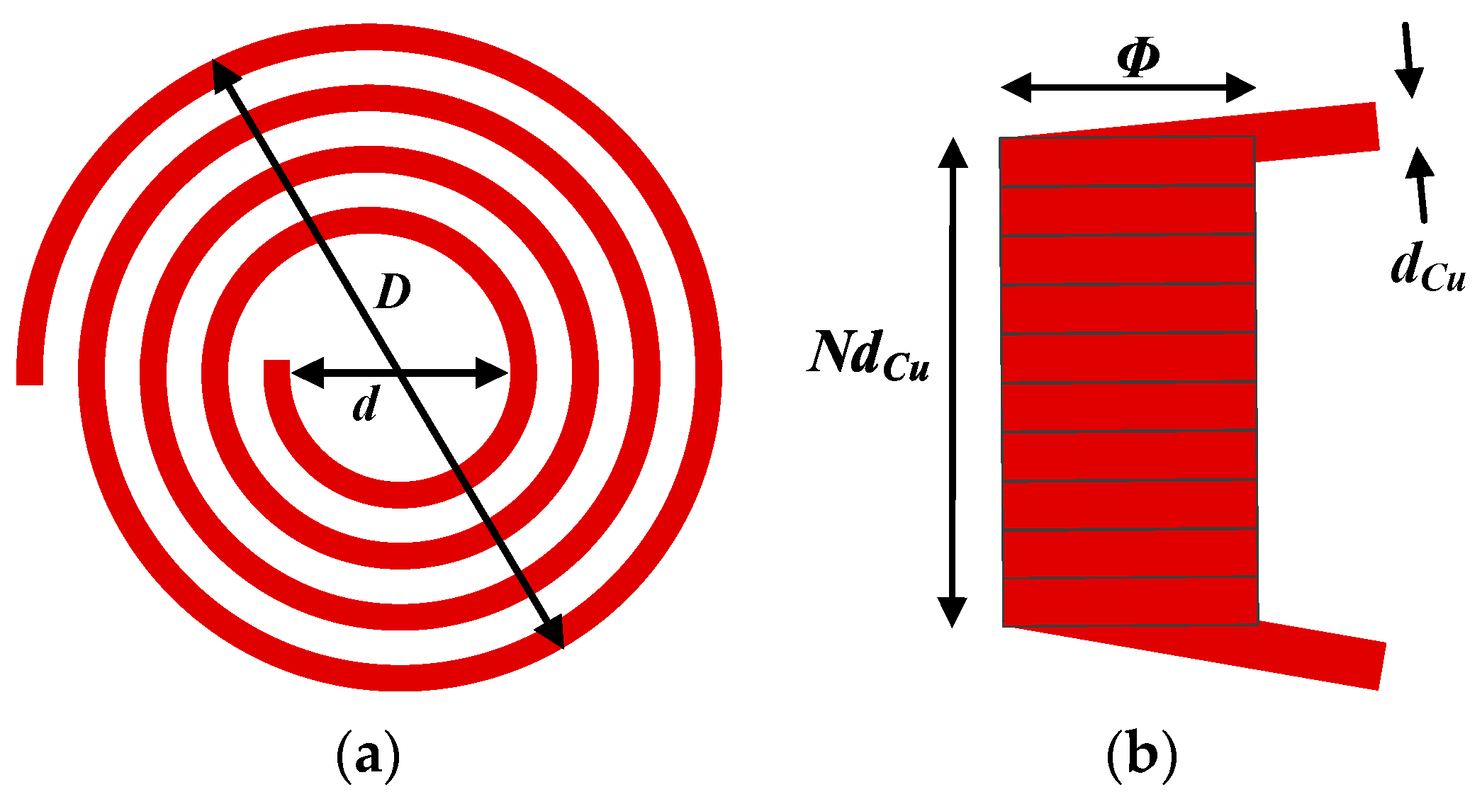
According to the profile, air-core inductors are classified into planar spiral inductors and solenoid inductors, as shown in Figure 7, which are discussed in the following sections.
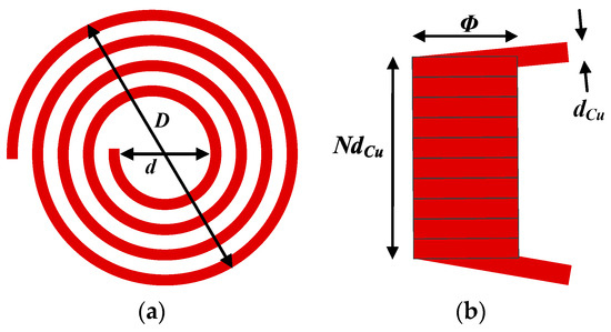
Figure 7.
Structure schematics of air-core inductors: (a) planar spiral inductor (b) solenoid inductor.
3.1. Winding Structure Optimization of Planar Spiral Inductors
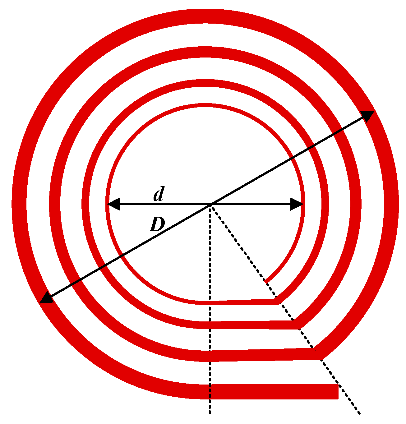
For a planar spiral inductor, the outer diameter, D, inner diameter, d, coil turn, N, coil-wire thickness and width determine its profile and inductance value. Inductance values of planar spiral inductors with different winding structures are uniformly expressed as follows [40]:
where D and d are the outer diameter and inner diameter, respectively, T is the ratio of difference and sum between outer and inner diameters, and N is the coil turn. The coefficients q1, q2, q3 and q4 of different winding structures are given in Table 3.
Table 3.
Coefficients p, q1, q2, q3 and q4 in different winding structures of planar spiral inductors.
Considering skin effect and coil length, the nth harmonic AC resistance values of planar spiral inductors are given by
where the coefficient, p, of different winding structures are as given in Table 3.
Combining (13) and (14), the quality factor of planar spiral inductors is derived as
According to (15), the quality factor depends on the cross-section perimeter, φ, coil turn, N, and T. For φ and N, the quality factor increases monotonically with them. For T, the function-related T in Q is defined as
Based on (16), the relationships between F and T are plotted in Figure 8 (T < 1). According to Figure 8, at the same D (area constraint), increasing d is beneficial for improving quality factor, Q.
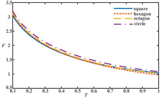
Figure 8.
Relationships between F and T at different winding structures of planar spiral inductors.
In general, the outer diameter D is constrained by the inductance value. In order to improve the quality factor, d, N and φ should increase as much as possible. However, the above measures are contradictory in the winding structures of equal width. Therefore, in [41], wide outside winding and the narrow inside winding are applied to improve the quality factor, as shown in Figure 9. The quality factor of the proposed winding structure is calculated using the Greenhouse algorithm. Each turn of the winding structure is approximated as a polygon. The inductance value is the sum of self inductances and mutual inductances of all turns. The AC resistance value is the sum of AC resistance values for all turns. Therefore, the quality factor can be calculated based on the inductance and AC resistance values.

Figure 9.
Wide outside winding and narrow inside winding structures of planar spiral inductors.
3.2. Winding Structure Optimization of Solenoid Inductors
For a tightly winding solenoid inductor, the winding diameter, ϕ, coil turn, N, and coil section diameter, dCu, determine its profile and inductance value. When the winding structure is cylinder, the inductance value of the solenoid inductor is given by [40] the following:
where Nagaoka’s coefficient, k, depends on ϕ/(NdCu), as given in Table 4.
Table 4.
Nagaoka’s coefficients with ϕ/(NdCu).
The length of the solenoid inductor is given by
Combining (14), (17) and (18), the quality factor of the solenoid inductor is derived as
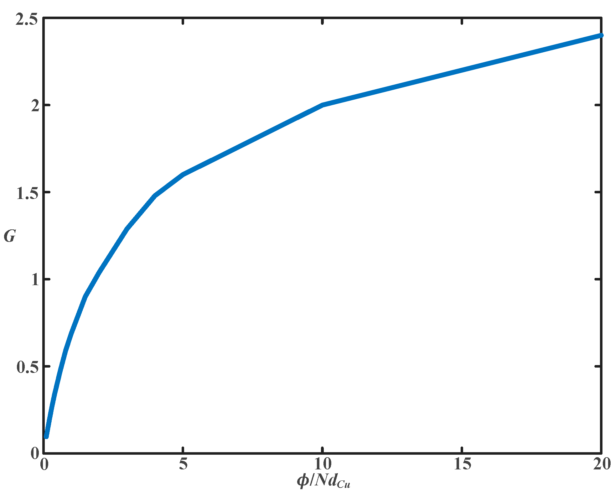
According to (19), the quality factor depends on N, dCu and ϕ. For N and dCu, the quality factor increases monotonically with them. For ϕ, the function -related ϕ in Q is defined as
Based on Table 4 and (20), the approximation relationship between G and ϕ/(NdCu) is plotted in Figure 10. According to Figure 10, at the same NdCu, increasing ϕ is beneficial for improving quality factor, Q, which causes the large volume. Unlike in planar spiral inductors, there is no optimized structure to improve the quality factor.

Figure 10.
Approximation relationship between G and ϕ/(NdCu).
4. Efficiency Boundary Prediction of PSiP
Power losses of PSiPs mainly include power losses of switches and inductors. Only considering power losses of inductors and power switches, the PoL power supply efficiency is expressed as
where Po, Pind and Pswitch are the output power, power losses of inductors and power switches, respectively.
In order to calculate the power losses of switches and inductors with the consideration of switching frequencies and power levels, Vin = 5 V, Vo = 1.8 V, fs = 1~100 MHz, △iL/IL0 = 0.4 and Po = 0.1~10 W are used in calculations.
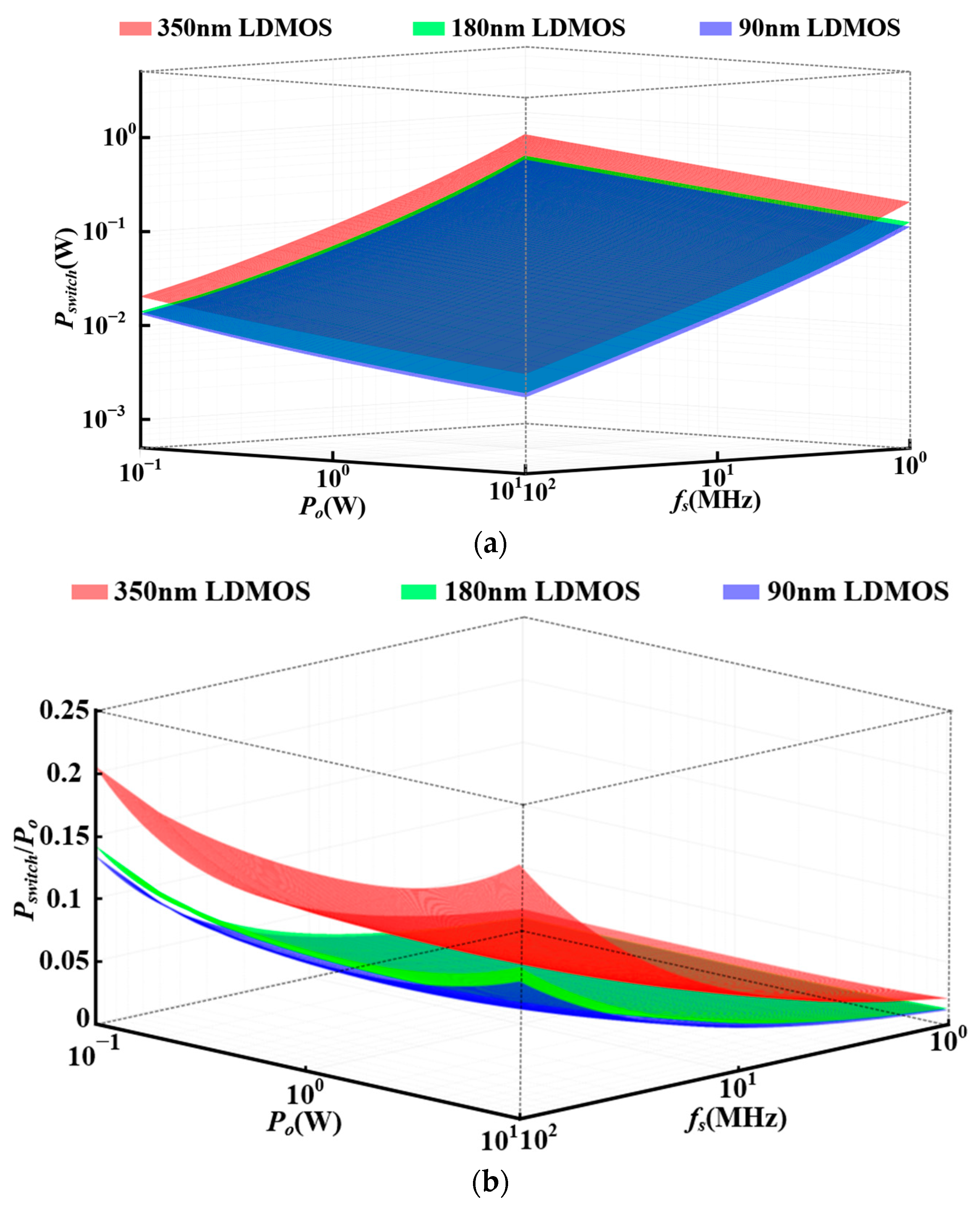
For the power loss of integrated Si LDMOSFETs, optimized sizes of integrated Si LDMOSFETs at 350 nm, 180 nm and 90 nm processes are calculated at different switching frequencies and output currents according to (7) and (10). The parameters of optimized integrated Si MOSFETs are given in Table 5. As the switching frequency increases, the RDS of integrated Si MOSFET increases, and CISS, CRSS and COSS decrease, which trades off power losses among switching loss, driving loss and conduction loss. Furthermore, based on the parameters of Si LDMOSFETs, the power losses of Si LDMOSFETs, Pswitch, at 350 nm, 180 nm and 90 nm are shown in Figure 11a. Furthermore, the efficiency boundary, Pswitch/Po, is calculated as shown in Figure 11b.
Table 5.
Parameters of Integrated Si MOSFETS with Optimal Sizes at Different Frequencies.

Figure 11.
Power losses of switches, Pswitch and Pswitch/Po, with switching frequency and power level of (a) Pswitch (b) Pswitch/Po.
In Figure 11a, the optimized power loss of the integrated Si LDMOSFET is proportional to fs1/2 instead of fs, which shows the potential for high-frequency switches. As the switching frequency increases, the power loss of the integrated Si LDMOSFET increases at a rate of fs1/2. As the power level increases, the power loss of the integrated Si LDMOSFET increases at a rate of Po. In addition, the power losses of the integrated LDMOSFEET under more advanced processes are reduced due to reductions of the parasitic capacitors and resistors.
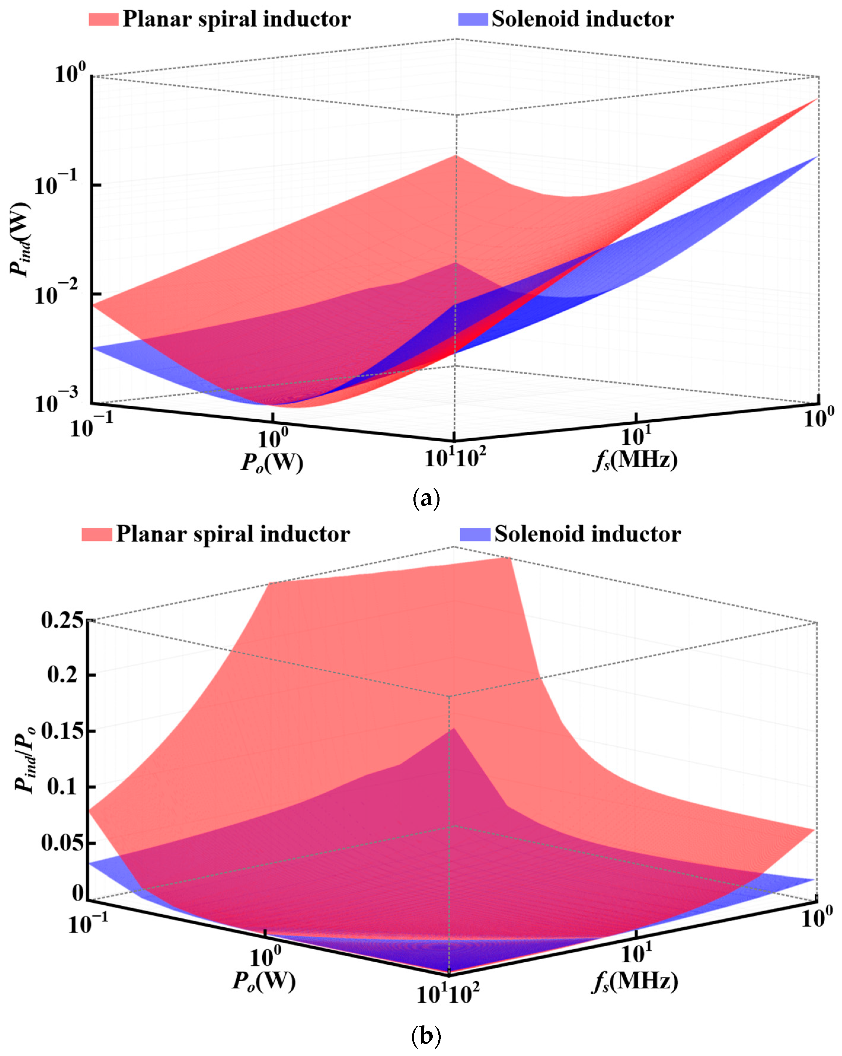
For the power loss of air-core inductors, the required inductance value is calculated according to the switching frequency and ripple ratio of the inductance current. Then, with consideration of the optimized winding structures, the geometric parameters (D, d, ϕ) are estimated based on the inductance value according to (13) and (17). Furthermore, based on (14) and (18), the coil length is calculated according to inductance geometric shapes. Finally, based on (11), the power losses of air-core inductors, Pind, with winding structure optimizations are shown in Figure 12a. Furthermore, the efficiency boundary, Pind/Po, is calculated as shown in Figure 12b. The following assumptions are introduced into the calculations according to common engineering values:

Figure 12.
Power losses of inductors, Pind and Pind/Po, with switching frequency and power level of (a) Pind (b) Pind/Po.
- For the tightly winding solenoid inductor, its wire width and coil turn are set as 1 mm and 10.
- For the planar spiral inductor, its thickness and coil turn are set as 100 μm and 10. Since it has a wide outside winding and narrow inside winding structure, its width is set as 1~2 mm.
In Figure 12a, as the switching frequency increases, the coil-wire length, l, and skin depth, δ, both decrease. Based on calculations, since the effect of coil-wire length reduction on power loss is greater than that of skin effect at 1~100 MHz, the power losses of air-core inductors decrease as the switching frequency increases. As the power level increases, the inductance current, IL, and ripple, △iL, increase. The increase of △iL results in reductions of inductance, L, and coil-wire length, l. Therefore, the power losses of air-core inductors are at the minimum value as the power level increases.
Combined with power loss calculations, Pswitch/Po and Pind/Po are shown in Figure 11b and Figure 12b. It can be seen that the main power losses at low and high frequencies are from switches and inductors, respectively. Therefore, the directions of further reduction of power losses at low frequency and high frequency are different. At low frequency, the sizes of air-core inductors are slightly increased to reduce their DC and AC resistance values. At high frequency, advanced processes are applied to reduce the parasitic capacitance values of Si LDMOSFETs. According to the above analysis, for reducing power loss to improve switching frequency, PSiPs need to optimize the size of the integrated Si MOSFET in advanced processes and optimize the winding structure of air-core inductors. At a high enough switching frequency, air-core inductors are integrated in the chip, which represents the trend from PSiP to PwrSoC. Reducing power loss is also a heat dissipation requirement for the highly integrated PwrSoC package.
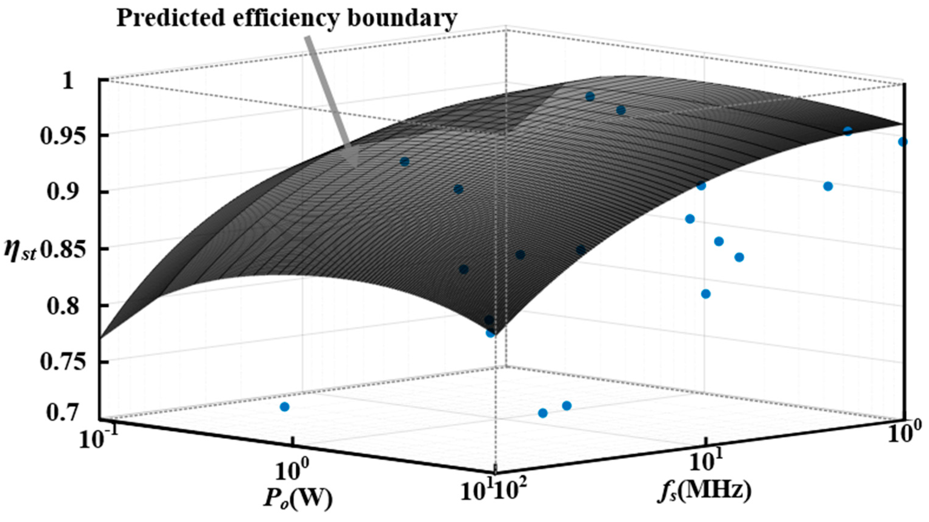
According to Figure 11b and Figure 12b, the efficiency boundaries of PSiPs are predicted and verified in Figure 13 [42,43,44,45,46,47,48,49,50,51,52,53,54,55,56,57,58,59,60,61]. In order to eliminate the effect of input and output voltages on efficiency, the efficiencies in the literature are normalized according to the following:
where ηst and η are efficiencies with and without normalization.

Figure 13.
Prediction and verification of the efficiency boundary [42,43,44,45,46,47,48,49,50,51,52,53,54,55,56,57,58,59,60,61].
In Figure 13, the efficiencies found in state-of-the-art research are lower than those of the predicted efficiency boundary, and most of them are close to the boundary, which verifies the prediction based on the power loss analysis. The predicted errors are mainly from power losses of the equivalent series resistor and controller. The above optimized measures reduce power losses and improve efficiency, which provides roadmaps for achieving high-frequency PSiPs.
5. Conclusions
This paper provides power loss optimizations for PSiPs in relation to integrated Si LDMOSFETs and air-core inductors. For integrated Si LDMOSFETs, a size and parallel quantity optimization is provided based on power loss analyzation. For air-core inductors, quality factors are improved by winding structure optimization to reduce coil loss. The power losses of the integrated Si LDMOSFET and air-core inductor are both reduced to less than 10% of the output power at 1~100 MHz switching frequency and 0.1~10 W power level. Based on the analysis, this paper predicts the efficiency boundary of PSiPs. The efficiency prediction error is 1~15% at 1~100 MHz switching frequency and 0.1~10 W power level. The predicted results are consistent with the findings of state-of-the-art research. To improve the efficiency toward high-frequency PSiP, two technologies are proposed from the perspective of switches and inductors.
- For power switches, a parallel quantity of integrated Si LDMOSFET is designed based on power level. The size of each power switch is optimized based on switching frequency and power level.
- For power inductors, the planar spiral inductor provides a low profile for monolithic integration. An optimal winding structure with narrow inner and wider outer windings dramatically reduces power losses.
Author Contributions
Conceptualization, Y.W. and R.M.; methodology, Y.W. and D.Z.; software, Y.W. and B.H.; validation, L.L. and H.X.; formal analysis, Y.W., H.X. and R.M..; investigation, Y.W. and D.Z.; resources, L.L., B.H and X.Z.; data curation, Y.W. and X.Z.; writing—original draft preparation, Y.W.; writing—review and editing, Y.W., D.Z., H.X. and R.M.; visualization, X.Z.; supervision, X.Z.; project administration, Y.W., R.M. and X.Z.; funding acquisition, R.M. and X.Z. All authors have read and agreed to the published version of the manuscript.
Funding
This research received no external funding.
Institutional Review Board Statement
Not applicable.
Informed Consent Statement
Not applicable.
Conflicts of Interest
The authors declare no conflict of interest.
Nomenclature
| fs | Switching frequency |
| Vin | Input voltage of PoL power supply |
| Vout | Output voltage of PoL power supply |
| IL0, ILn | DC value and nth harmonic amplitude of inductance current |
| ΔiL | Ripple of inductance current |
| Io | Load current of PoL power supply |
| CGD | Capacitance between gate and drain of integrated Si LDMOSFT |
| CGS | Capacitance between gate and source of integrated Si LDMOSFT |
| CDS | Capacitance between drain and source of integrated Si LDMOSFT |
| CISS | Input capacitance of integrated Si LDMOSFET |
| COSS | Output capacitance of integrated Si LDMOSFET |
| CRSS | Reverse transfer capacitance of integrated Si LDMOSFET |
| RG | Gate resistance of integrated Si LDMOSFET |
| Ron | Drain-source on-resistance of integrated Si LDMOSFET |
| VDS | Drain and source voltage of integrated Si LDMOSFT |
| VGS | Gate and source voltage of integrated Si LDMOSFT |
| IDS | Drain and source current of integrated Si LDMOSFT |
| VPL | Miller voltage of integrated Si LDMOSFT |
| Vth | Gate threshold voltage of integrated Si LDMOSFT |
| VDD | Power supply voltage of driver |
| mn | Electron mobility |
| WM | Channel width of integrated Si LDMOSFET |
| LM | Channel length of integrated Si LDMOSFET |
| EM | Drain/source width of integrated Si LDMOSFET |
| Cox | Gate oxide capacitance per unit area of integrated Si LDMOSFET |
| Cov | Gate-to-source/drain overlap capacitance per unit width of integrated Si LDMOSFET |
| Cj | Source/drain junction capacitance per unit area of integrated Si LDMOSFET |
| Cjsw | Source/drain sidewall junction capacitance per unit length of integrated Si LDMOSFET |
| L | Inductance value |
| l | Coil-wire length of inductor |
| A, φ | Cross-section area and perimeter of inductance coil-wire |
| μ0 | Space permeability |
| ρ | Resistivity of inductance coil-wire material |
| δn | Skin depth of nth harmonic inductance current |
| RDC, RAC,n | DC and nth harmonic AC equivalent resistances of inductor |
References
- Lin, H.; Van der Plas, G.; Sun, X.; Velenis, D.; Beyne, E.; Lauwereins, R. System Optimization: High-Frequency Buck Converter with 3D In-Package Air-Core Inductor. IEEE Trans. Compon. Packag. Manuf. Technol. 2021, 12, 401–409. [Google Scholar] [CrossRef]
- Sun, Q.; Ma, Y.; Ye, Z.; Wang, X.; Zhang, H. A Pseudo-Constant Frequency Constant On-Time Buck Converter with Internal Current Ripple Injection and Output DC Offset Cancellation. IEEE Access 2019, 7, 175443–175453. [Google Scholar] [CrossRef]
- Seo, G.; Das, R.; Le, H. Dual Inductor Hybrid Converter for Point-of-Load Voltage Regulator Modules. IEEE Trans. Ind. Appl. 2020, 56, 367–377. [Google Scholar] [CrossRef]
- Hernandez, J.C.; Mira, M.C.; Petersen, L.P.; Andersen, M.A.E.; Petersen, N.H. Zero Voltage Switching Control Method for MHz Boundary Conduction Mode Converters. IEEE Trans. Ind. Electron. 2020, 67, 1544–1554. [Google Scholar] [CrossRef]
- Wang, K.; Qi, Z.; Li, F.; Wang, L.; Yang, X. Review of state-of-the-art integration technologies in power electronic systems. CPSS Trans. Power Electron. Appl. 2017, 2, 292–305. [Google Scholar] [CrossRef]
- Feeney, C.; Wang, N. A new Electronic Design Automation tool for the optimization of PwrSoC/PwrSiP DC-DC converters. In Proceedings of the 2018 IEEE Applied Power Electronics Conference and Exposition (APEC), San Antonio, TX, USA, 4–8 March 2018; pp. 2905–2909. [Google Scholar]
- Doyle, J.T.; Stiff, J.C.; Kulkarni, S.; Yildiz, A. A Low Cost 100 MHz 2-Stage PSiP and Evolution to a Co-Packaged/Fully-Integrated Voltage Regulator for SoC Power Delivery. In Proceedings of the 2019 IEEE Custom Integrated Circuits Conference (CICC), Austin, TX, USA, 14–17 April 2019; pp. 1–8. [Google Scholar]
- You, X.; Sun, X.; Fei, J.; Zhang, M.; Zhang, B.; Chen, T.; Qin, Y.; Rong, N.; Wan, C. A Gallium-Nitride Point-of-load DC-DC Converter for Space Applications. In Proceedings of the 2019 European Space Power Conference (ESPC), Juan-les-Pins, France, 30 September–4 October 2019; pp. 1–6. [Google Scholar]
- Qi, Z.; Zhao, C.; Wang, L.; Yang, F.; Pei, Y.; Zheng, Z. Three-Dimensional Integrated GaN-based DC-DC Converter with an Inductor Substrate. In Proceedings of the 2019 IEEE Energy Conversion Congress and Exposition (ECCE), Baltimore, MD, USA, 29 September–3 October 2019; pp. 832–838. [Google Scholar]
- Yu, L.; Mu, W.; Li, H.; Yang, C.; Wang, C.; Wang, L. An Integrated GaN-Based Converter Based on Cooling-System-Inductor Structure for point-of-load converters. In Proceedings of the 2021 IEEE Workshop on Wide Bandgap Power Devices and Applications in Asia (WiPDA Asia), Wuhan, China, 25–27 August 2021; pp. 236–240. [Google Scholar]
- Waldron, F.; Foley, R.; Slowey, J.; Alderman, A.N.; Narveson, B.C.; Mathúna, S.C.Ó. Technology Roadmapping for Power Supply in Package (PSiP) and Power Supply on Chip (PwrSoC). IEEE Trans. Power Electron. 2013, 28, 4137–4145. [Google Scholar] [CrossRef]
- Tang, N.; Nguyen, B.; Tang, Y.; Hong, W.; Zhou, Z.; Heo, D. Fully Integrated Buck Converter with 78% Efficiency at 365mW Output Power Enabled by Switched-Inductor Capacitor Topology and Inductor Current Reduction Technique. In Proceedings of the 2019 IEEE International Solid-State Circuits Conference—(ISSCC), San Francisco, CA, USA, 17–21 February 2019; pp. 152–154. [Google Scholar]
- Amin, S.S.; Mercier, P.P. A Fully Integrated Li-Ion-Compatible Hybrid Four-Level DC–DC Converter in 28-nm FDSOI. IEEE J. Solid-State Circuits 2019, 54, 720–732. [Google Scholar] [CrossRef]
- Renz, P.; Kaufmann, M.; Lueders, M.; Wicht, B. A Fully Integrated 85%-Peak-Efficiency Hybrid Multi Ratio Resonant DC-DC Converter with 3.0-to-4.5V Input and 500μA-to-120mA Load Range. In Proceedings of the 2019 IEEE International Solid-State Circuits Conference—(ISSCC), San Francisco, CA, USA, 17–21 February 2019; pp. 156–158. [Google Scholar]
- Schrom, G.; Vunnam, R.S.; Makala, S.; Lyakhov, A. High-Speed ZVS-ZCS Soft-Switching CMOS Bridge Drivers for a DC-DC Fully Integrated Voltage Regulator (FIVR) operating at 100–320 MHz on 22 nm process node. In Proceedings of the 2019 IEEE Applied Power Electronics Conference and Exposition (APEC), Anaheim, CA, USA, 17–21 March 2019; pp. 2263–2267. [Google Scholar]
- Udabe, A.; Baraia-Etxaburu, I.; Diez, D.G. Gallium Nitride Power Devices: A State of the Art Review. IEEE Access 2023, 11, 48628–48650. [Google Scholar] [CrossRef]
- Reusch, D.; Strydom, J. Understanding the Effect of PCB Layout on Circuit Performance in a High-Frequency Gallium-Nitride-Based Point of Load Converter. IEEE Trans. Power Electron. 2014, 29, 2008–2015. [Google Scholar] [CrossRef]
- Reusch, D.; Gilham, D.; Su, Y.; Lee, F.C. Gallium Nitride based 3D integrated non-isolated point of load module. In Proceedings of the 2012 Twenty-Seventh Annual IEEE Applied Power Electronics Conference and Exposition (APEC), Orlando, FL, USA, 5–9 February 2012; pp. 38–45. [Google Scholar]
- Ujita, S.; Kinoshita, Y.; Umeda, H.; Morita, T.; Kaibara, K.; Tamura, S.; Ishida, M.; Ueda, T. A fully integrated GaN-based power IC including gate drivers for high-efficiency DC-DC Converters. In Proceedings of the 2016 IEEE Symposium on VLSI Circuits (VLSI-Circuits), Honolulu, HI, USA, 15–17 June 2016; pp. 1–2. [Google Scholar]
- Yu, L.; Mu, W.; Yang, C.; Zhu, L.; Qi, Z.; Wang, L.; Yao, Y.; Su, Y.; Zhang, C. Symmetric Four-Phase Inverse Coupled Inductors for GaN-Based Interleaving Four-Phase Point-of-load Converters. In Proceedings of the 2021 IEEE Energy Conversion Congress and Exposition (ECCE), Vancouver, BC, Canada, 10–14 October 2021; pp. 5453–5458. [Google Scholar]
- Cook, T.; Phillips, A.; Siak, C.; George, A.D.; Grainger, B.M. Evaluation of Point of Load Converters for Space Computational Loads. In Proceedings of the 2020 IEEE Aerospace Conference, Big Sky, MT, USA, 7–14 March 2020; pp. 1–12. [Google Scholar]
- AlMukhtar, B.; Harriman, P.; Burke, K. The analysis of multi-phase current feedforward type-III constant on-time control with ultrafast load transient response for voltage regulator modules. In Proceedings of the 2016 IEEE International Conference on Electronics, Circuits and Systems (ICECS), Monte Carlo, Monaco, 11–14 December 2016; pp. 201–204. [Google Scholar]
- Available online: https://product.tdk.com/en/products/ferrite/index.html (accessed on 9 December 2023).
- Available online: https://www.mag-inc.com/Products/Powder-Cores/Magnetics-Powder-Core-Material-Property-Curves/Permeability-versus-Frequency-Curves-for-Powder-Co (accessed on 9 December 2023).
- Available online: https://www.mag-inc.com/Products/Tape-Wound-Cores/Nanocrystalline/Nanocrystalline-Material-Property-Curves (accessed on 9 December 2023).
- Le, H.T.; Nour, Y.; Pavlovic, Z.; Mathúna, C.O.; Knott, A.; Jensen, F.; Han, A.; Kulkarni, S.; Ouyang, Z. High-Q Three-Dimensional Microfabricated Magnetic-Core Toroidal Inductors for Power Supplies in Package. IEEE Trans. Power Electron. 2019, 34, 74–85. [Google Scholar] [CrossRef]
- Liu, J.; Mei, Y.; Lu, S.; Li, X.; Lu, G. Continuously Variable Multi-Permeability Inductor for Improving the Efficiency of High-Frequency DC–DC Converter. IEEE Trans. Power Electron. 2020, 35, 826–834. [Google Scholar] [CrossRef]
- Schaef, C.; Desai, N.; Krishnamurthy, H.K.; Liu, X.; Ahmed, K.Z.; Kim, S.; Weng, S.; Do, H.; Lambert, W.J.; Radhakrishnan, K.; et al. A Light-Load Efficient Fully Integrated Voltage Regulator in 14-nm CMOS with 2.5-nH Package-Embedded Air-Core Inductors. IEEE J. Solid-State Circuits 2019, 54, 3316–3325. [Google Scholar] [CrossRef]
- Available online: https://www.coilcraft.com/en-us/products/rf/air-core-inductors/#/ (accessed on 9 December 2023).
- Krishnamurthy, H.K.; Vaidya, V.; Weng, S.; Ravichandran, K.; Kumar, P.; Kim, S.; Jain, R.; Matthew, G.; Tschanz, J.; De, V. A digitally controlled fully integrated voltage regulator with on-die solenoid inductor with planar magnetic core in 14 nm tri-gate CMOS. In Proceedings of the 2017 IEEE International Solid-State Circuits Conference (ISSCC), San Francisco, CA, USA, 5–9 February 2017; pp. 336–337. [Google Scholar]
- Krishnamurthy, H.K.; Weng, S.; Mathew, G.E.; Desai, N.; Saraswat, R.; Ravichandran, K.; Tschanz, J.W.; De, V. A Digitally Controlled Fully Integrated Voltage Regulator with 3-D-TSV-Based On-Die Solenoid Inductor with a Planar Magnetic Core for 3-D-Stacked Die Applications in 14-nm Tri-Gate CMOS. IEEE J. Solid-State Circuits 2018, 53, 1038–1048. [Google Scholar] [CrossRef]
- Abdulslam, A.; Mohammad, B.; Ismail, M.; Mercier, P.P.; Ismail, Y. A 93% Peak Efficiency Fully-Integrated Multilevel Multistate Hybrid DC–DC Converter. IEEE Trans. Circuits Syst. I Regul. Pap. 2018, 65, 2617–2630. [Google Scholar] [CrossRef]
- Nour, Y.; Ouyang, Z.; Knott, A.; Jørgensen, I.H.H. Design and implementation of high frequency buck converter using multi-layer PCB inductor. In Proceedings of the IECON 2016—42nd Annual Conference of the IEEE Industrial Electronics Society, Florence, Italy, 23–26 October 2016; pp. 1313–1317. [Google Scholar]
- Lee, M.; Choi, Y.; Kim, J. A 500-MHz, 0.76-W/mm Power Density and 76.2% Power Efficiency, Fully Integrated Digital Buck Converter in 65-nm CMOS. IEEE Trans. Ind. Appl. 2016, 52, 3315–3323. [Google Scholar] [CrossRef]
- Musunuri, S.; Chapman, P.L. Optimization of CMOS Transistors for Low Power DC-DC Converters. In Proceedings of the 2005 IEEE 36th Power Electronics Specialists Conference, Recife, Brazil, 16 June 2005; pp. 2151–2157. [Google Scholar]
- Qahouq, J.A.A.; Abdel-Rahman, O.; Huang, L.; Batarseh, I. On Load Adaptive Control of Voltage Regulators for Power Managed Loads: Control Schemes to Improve Converter Efficiency and Performance. IEEE Trans. Power Electron. 2007, 22, 1806–1819. [Google Scholar] [CrossRef]
- Razavi, B. Design of Analog CMOS Integrated Circuits; McGraw-Hill Education: New York, NY, USA, 2001. [Google Scholar]
- Jia, T.; Gu, J. A Fully Integrated Buck Regulator with 2-GHz Resonant Switching for Low-Power Applications. IEEE J. Solid-State Circuits 2018, 53, 2663–2674. [Google Scholar] [CrossRef]
- Kudva, S.S.; Harjani, R. Fully integrated on-chip DC-DC converter with a 450x output range. In Proceedings of the IEEE Custom Integrated Circuits Conference 2010, San Jose, CA, USA, 19–22 September 2010; pp. 1–4. [Google Scholar]
- Kazimierczuk, M.K. High-Frequency Magnetic Components; John Wiley & Sons: Hoboken, NJ, USA, 2009. [Google Scholar]
- Guan, Y.; Wang, Y.; Wang, W.; Xu, D. A 20 MHz Low-Profile DC–DC Converter with Magnetic-Free Characteristics. IEEE Trans. Ind. Electron. 2020, 67, 1555–1567. [Google Scholar] [CrossRef]
- Park, J.; Lee, H.M.; Shin, S.U.; Choi, W.; Hong, S.W. A 0.46 mm2 On-Chip Compensated Type-III Buck Converter Using an Inner Feedback Loop with a Seamless CCM/DCM Transition Technique. IEEE Trans. Power Electron. 2020, 35, 4477–4482. [Google Scholar] [CrossRef]
- Huang, Q.; Zhan, C.; Burm, J. A 4-MHz Digitally Controlled Voltage-Mode Buck Converter with Embedded Transient Improvement Using Delay Line Control Techniques. IEEE Trans. Circuits Syst. I Regul. Pap. 2020, 67, 4029–4040. [Google Scholar] [CrossRef]
- Hong, W.; Lee, M. A 7.4-MHz Tri-Mode DC-DC Buck Converter with Load Current Prediction Scheme and Seamless Mode Transition for IoT Applications. IEEE Trans. Circuits Syst. I Regul. Pap. 2020, 67, 4544–4555. [Google Scholar] [CrossRef]
- Huang, W.; Liu, L.; Liao, X.; Xu, C.; Li, Y. A 240-nA Quiescent Current, 95.8% Efficiency AOT-Controlled Buck Converter with A2-Comparator and Sleep-Time Detector for IoT Application. IEEE Trans. Power Electron. 2021, 36, 12898–12909. [Google Scholar] [CrossRef]
- Ahmed, M.S.; Fayed, A.A. A Current-Mode Delay-Based Hysteretic Buck Regulator with Enhanced Efficiency at Ultra-Light Loads for Low-Power Microcontrollers. IEEE Trans. Power Electron. 2020, 35, 471–483. [Google Scholar] [CrossRef]
- Chen, J.J.; Hwang, Y.S.; Ku, Y.; Li, Y.H.; Chen, J.A. A Current-Mode-Hysteretic Buck Converter with Constant-Frequency-Controlled and New Active-Current-Sensing Techniques. IEEE Trans. Power Electron. 2021, 36, 3126–3134. [Google Scholar] [CrossRef]
- Yuan, B.; Liu, M.X.; Ng, W.T.; Lai, X.Q. A Fast-Response RBAOT-Controlled Buck Converter with Pseudofixed Switching Frequency and Enhanced Output Accuracy. IEEE J. Emerg. Sel. Top. Power Electron. 2021, 9, 79–88. [Google Scholar] [CrossRef]
- Qu, Y.; Shu, W.; Chang, J.S. A Fully Soft Switched Point-of-Load Converter for Resource Constraint Drone Applications. IEEE Trans. Power Electron. 2020, 35, 2705–2713. [Google Scholar] [CrossRef]
- Chen, J.J.; Hwang, Y.S.; Wu, J.H.; Lai, C.H.; Ku, Y.T. A New Improved V-Square-Controlled Buck Converter with Rail-to-Rail OTA-Based Current-Sensing Circuits. IEEE Trans. Very Large Scale Integr. (VLSI) Syst. 2021, 29, 1428–1436. [Google Scholar] [CrossRef]
- Ting, C.Y.; Lin, J.Y.; Chen, C.C.P. A Quasi-V2 Hysteretic Buck Converter with Adaptive COT Control for Fast DVS and Load-Transient Response in RF Applications. IEEE Trans. Circuits Syst. II Express Briefs 2020, 67, 531–535. [Google Scholar] [CrossRef]
- Qu, Y.; Shu, W.; Chang, J. An Air-Core Coupled-Inductor Based Dual-Phase Output Stage for Point-of-Load Converters. In Proceedings of the 2018 IEEE International Symposium on Circuits and Systems (ISCAS), Florence, Italy, 27–30 May 2018; pp. 1–4. [Google Scholar]
- Ting, C.Y.; Ko, C.C.; Lin, J.Y.; Chen, C.C.P. An Inductor Current Balancing Technique for FLDLL Based Four-phase Buck Converter with Transient-modulated Constant On-time Control for Load Transient Response. In Proceedings of the 2019 4th International Conference on Intelligent Green Building and Smart Grid (IGBSG), Yichang, China, 6–9 September 2019; pp. 1–4. [Google Scholar]
- Chen, J.J.; Hwang, Y.S.; Tzeng, T.S.; Lai, C.H.; Ku, J. A Low-Noise Fast-Transient-Response Delta-Sigma-Modulation Buck Converter with Hysteresis-Voltage-Controlled Techniques. IEEE Access 2022, 10, 63063–63072. [Google Scholar] [CrossRef]
- Wang, C.; Lu, Y.; Huang, M.; Martins, R.P. A Two-Phase Three-Level Buck Converter with Cross-Connected Flying Capacitors for Inductor Current Balancing. IEEE Trans. Power Electron. 2021, 36, 13855–13866. [Google Scholar] [CrossRef]
- Lee, C.H.; Park, H.J.; Cho, J.M.; Choi, H.J.; Park, S.M.; Baik, E.; Oh, Y.J.; Ahn, H.C.; Lee, C.K.; Shin, J.; et al. An Input-Independent Loop Type-III Buck Converter with PSRR Improvement and EMI Suppression for Enhancing the Security of Edge Devices. IEEE Trans. Power Electron. 2022, 37, 10070–10074. [Google Scholar] [CrossRef]
- Huang, Y.W.; Kuo, T.H. Fixed-Switching-Frequency Background Capacitor-Current-Sensor Calibration for DC–DC Converters. IEEE Journal of Solid-State Circuits 2022, 57, 1504–1516. [Google Scholar] [CrossRef]
- Seo, J.I.; Lim, B.M.; Choi, W.J.; Noh, Y.S.; Lee, S.G. A 95.1% Efficiency Hybrid Hysteretic Reconfigurable 3-Level Buck Converter with Improved Load Transient Response. IEEE Trans. Power Electron. 2022, 37, 14916–14925. [Google Scholar] [CrossRef]
- Wang, C.; Lu, Y.; Martins, R.P. A Highly Integrated Tri-Path Hybrid Buck Converter with Reduced Inductor Current and Self-Balanced Flying Capacitor Voltage. IEEE Trans. Circuits Syst. I Regul. Pap. 2022, 69, 3841–3850. [Google Scholar] [CrossRef]
- Kim, S.; Krishnamurthy, H.K.; Amin, S.S.; Weng, S.; Feng, J.; Do, H.; Radhakrishnan, K.; Ravichandran, K.; Tschanz, J.W.; De, V. A 1S Direct-Battery-Attach Buck Voltage Regulator with 5-Stack Thin-Gate 22-nm FinFET CMOS Featuring Active Voltage Balancing and Cascaded Self-Turn-ON Drivers. IEEE Solid-State Circuits Lett. 2021, 4, 234–237. [Google Scholar] [CrossRef]
- Huang, Y.W.; Yu, T.Y.; Kuo, T.H. Transient Output-Current Regulator with Background Calibration Applied to a Buck Converter for Fast Load-Transient Response. IEEE Solid-State Circuits Lett. 2020, 3, 462–465. [Google Scholar] [CrossRef]


Disclaimer/Publisher’s Note: The statements, opinions and data contained in all publications are solely those of the individual author(s) and contributor(s) and not of MDPI and/or the editor(s). MDPI and/or the editor(s) disclaim responsibility for any injury to people or property resulting from any ideas, methods, instructions or products referred to in the content. |
© 2023 by the authors. Licensee MDPI, Basel, Switzerland. This article is an open access article distributed under the terms and conditions of the Creative Commons Attribution (CC BY) license (https://creativecommons.org/licenses/by/4.0/).