Article

Large Field-Size Elliptic Curve Processor for Area-Constrained Applications

1
Computer Engineering Department, Umm Al Qura University, Makkah 21955, Saudi Arabia
2
Department of Electrical Engineering, Ziauddin University, Karachi 74600, Pakistan
3
Telecommunications Engineering School, University of Malaga, 29010 Málaga, Spain
4
Department of Computer Science, National University of Computer and Emerging Sciences, Karachi 75030, Pakistan
5
Computer Science Department, Umm Al Qura University, Makkah 21955, Saudi Arabia
*
Authors to whom correspondence should be addressed.
Appl. Sci. 2023, 13(3), 1240; https://doi.org/10.3390/app13031240
Submission received: 27 November 2022 / Revised: 9 January 2023 / Accepted: 13 January 2023 / Published: 17 January 2023

Abstract

:
This article has proposed an efficient area-optimized elliptic curve cryptographic processor architecture over G F ( 2 409 ) and G F ( 2 571 ) . The proposed architecture employs Lopez-Dahab projective point arithmetic operations. To do this, a hybrid Karatsuba multiplier of 4-split polynomials is proposed. The proposed multiplier uses general Karatsuba and traditional schoolbook multiplication approaches. Moreover, the multiplier resources are reused to implement the modular squares and addition chains of the Itoh-Tsujii algorithm for inverse computations. The reuse of resources reduces the overall area requirements. The implementation is performed in Verilog (HDL). The achieved results are provided on Xilinx Virtex 7 device. In addition, the performance of the proposed design is evaluated on ASIC 65 nm process technology. Consequently, a figure-of-merit is constructed to compare the FPGA and ASIC implementations. An exhaustive comparison to existing designs in the literature shows that the proposed architecture utilizes less area. Therefore, the proposed design is the right choice for area-constrained cryptographic applications.

1. Introduction

The public-key cryptographic standards (ECC [1] and RSA [2]) are vulnerable to quantum computers when running a Shor’s algorithm [3,4]. In 2022, the National Institute of Standards and Technology (NIST) has standardized new quantum-secure key encapsulation and digital signature algorithms [5]. However, the NIST-recommended quantum algorithms are not reasonable for securing area constrained cryptographic applications such as wireless sensor nodes (WSNs) [6,7], radio-frequency-identification-networks (RFID) [8,9], automotive vehicles [10], secure robotics communication [11], etc. The reason is the huge hardware resource requirements due to several hash computations, binomial and gaussian samplers for introducing noise in the algorithm(s), and many more [3]. Many researchers are predicting that 10–15 years are needed for the widespread deployment of quantum computers [3,12]. Based on this compliance, this article realizes a low-complexity hardware accelerator of present public-key algorithms over large key sizes for area-constrained cryptographic applications.
As compared to RSA, ECC ensures equivalent security with shorter key lengths. For example, 233 bits of ECC are required to achieve identical security to a 2048-bit RSA [2]. The shorter key length assures additional benefits such as low area, low power consumption, a lower channel bandwidth requirement for data transmitting over the unsecured channel, etc. Therefore, ECC is an appropriate public-key cryptographic algorithm for area-constraint devices and applications. The NIST has standardized elliptic curve parameters for prime, i.e.,  G F ( P ) , and binary, i.e.,  G F ( 2 m ) , fields [13]. The NIST-specified lengths are different for the prime field (192, 224, 256, 384, and 521) and binary field (163, 233, 283, 409 and 571). Furthermore, the prime field has been frequently targeted for software-based implementations [14]. On the other hand, the binary field is preferred for field-programmable gate arrays (FPGA) and application-specific integrated circuits (ASIC) [15,16,17,18,19,20,21,22,23,24,25].
In addition to key length and the selection of a particular field, the choice between polynomial and normal basis representations is also important. These representations are required to implement the finite field modular operations (addition, multiplication, square, and inversion). The polynomial basis provides efficient modular multiplications while the normal basis is more suitable for modular square implementations [14,26]. Furthermore, ECC offers two coordinate representations (affine and projective) to execute the required cryptographic operations. In comparison, the affine coordinate representation is more expensive in throughput as it needs an inversion operation [14,17,21,25]. Therefore, we have preferred projective coordinates to implement G F ( 2 409 ) and G F ( 2 571 ) fields with polynomial basis representations for our computations in this work. The reason behind the selection of large field lengths is to consider higher security as the higher key lengths specify the higher security.

1.1. Related Work

Elliptic curve point multiplication (ECPM) is the most critical part (from a computation point of view) in elliptic curves. The EPCM further depends on the computation of two more operations. These operations are point addition (PA) and point double (PD). The PA and PD computations depend on the execution of finite field addition, square, multiplication and inverse operations. Different hardware accelerators have been described in the literature to optimize the ECPM implementation. Nevertheless, the most recent architectures are described in [15,16,17,18,19,20,21,22,23,24,25].
A highly efficient architecture for ECPM computation on Koblitz curves is proposed in [15] over G F ( 2 163 ) to G F ( 2 571 ) . The selected PM algorithm allows the parallel processing of Frobenius maps and point additions. Moreover, to minimize the computational time and improve clock frequency, the scheduling of point addition operations is performed. A pipelined multiplier accumulator unit is used. Finally, the inversion is based on efficient addition chains for the reduction of clock cycles. In [16], a 6CC-6CC (clock cycle) dual-field ECPM architecture is proposed. A Karatsuba multiplier is utilized to compute efficient polynomial multiplications. The scheduling of addition operations minimizes the total number of required cycles. The results are provided on Xilinx Virtex 5 and Virtex 7 FPGA devices.
An efficient throughput over area ECC processor over binary elliptic curves is proposed in [17]. A segmented digit-serial finite field multiplier is utilized to reduce hardware resources. Moreover, the scheduling of addition operations reduces latency (i.e., the computational time for PM execution). The results are synthesized on Virtex 7 FPGA device over G F ( 2 163 ) to G F ( 2 571 ) fields. Another throughput over area efficient ECC processor is presented in [18]. The area is reduced by employing only a singular finite field multiplier. A 41-bit digit-parallel multiplier is used to compute finite field squares and multiplication operations. Throughput is optimized using a 2-stage pipelining and rescheduling of PA and PD computations. Over G F ( 2 163 ) to G F ( 2 571 ) fields, the implementations are provided on Virtex 7 and modern 16nm ASIC technology.
The authentication of IoT (Internet of Things) devices is generally performed using a Physical Unclonable Function (PUF). Therefore, the leakage of PUF responses in an authentication system reduces its privacy and security. To improve its security, an ECC-based PM algorithm with different key lengths is used in [19]. The hardware resources are reduced by reusing the underlying finite field computing units. Their circuit achieves a maximum of 135 MHz frequency on Virtex 6 device. The single ECPM computation takes 19.33, 22.36, 41.36 and 56.5 μ for 233, 283, 409 and 571 key lengths respectively.
The Weierstrass model of ECC is implemented in [15,16,17,18,19]. Nevertheless, these designs are vulnerable to side-channel attacks. Consequently, in order to prevent these side-channel attacks, Edward and Huff curve-based PM architectures have been described in [20,21,22,23,24,25]. The Edward and Huff curves (special models of ECC) provide unified PA and PD operations to execute the PM operation in ECC. On Xilinx FPGA devices, Edward curve architecture over G F ( P ) with P = 256 is implemented in [20,21]. Similarly, the FPGA implemented Edward curve designs over G F ( 2 233 ) is described in [22,23]. The 4-stage pipelined architectures of Huff curves over G F ( 2 233 ) on FPGA is implemented in [24,25].

1.2. Research Gap

Various architectural techniques such as pipelining, parallelism, and different flavor of finite field multipliers, i.e., digit-serial, digit-parallel, and bit-parallel, etc., have been utilized to optimize the performance of ECPM operation in [15,16,17,18,19,20,21,22,23,24,25]. However, due to their higher area complexity, these architectures are not suitable for applications related to secure robotics communication, WSNs, automotive vehicles, RFID, etc. Therefore, the objective of this work is to provide a low-complexity hardware accelerator over a large ECC field size.

1.3. Contributions

The contributions are given as follows:
  • We have presented an area-optimized hardware accelerator of a large field-size elliptic curve point multiplication processor over binary G F ( 2 409 ) and G F ( 2 571 ) fields. The design details are described in Section 3.
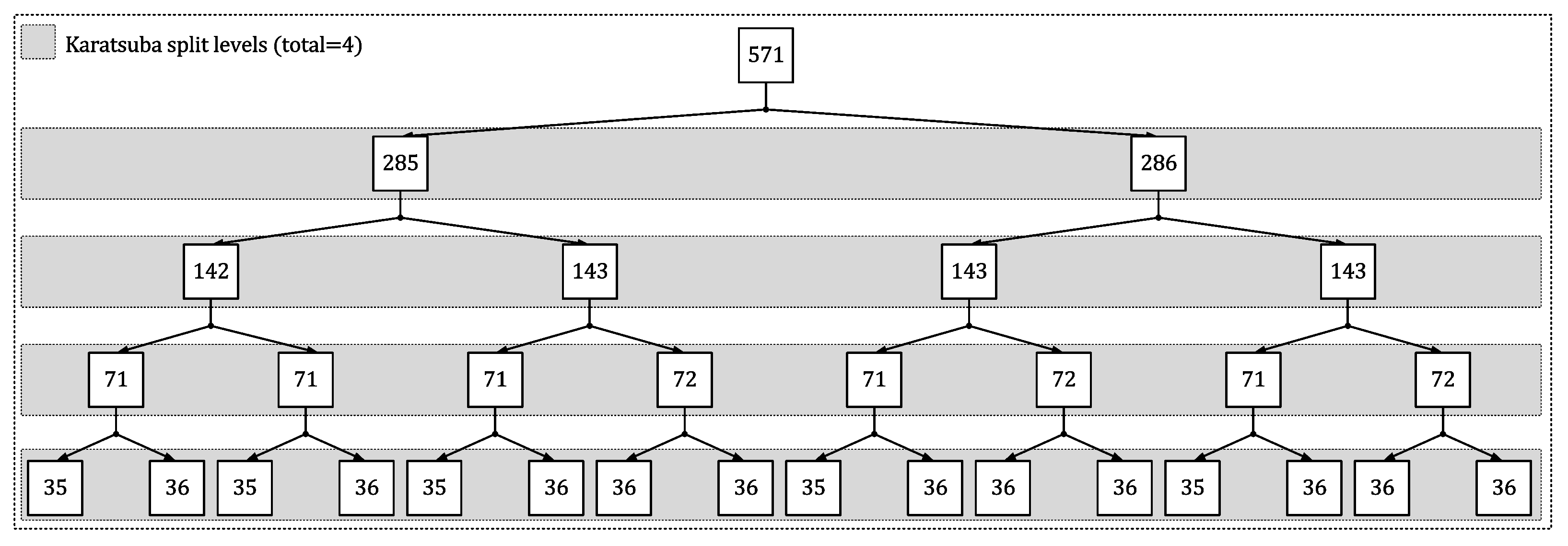
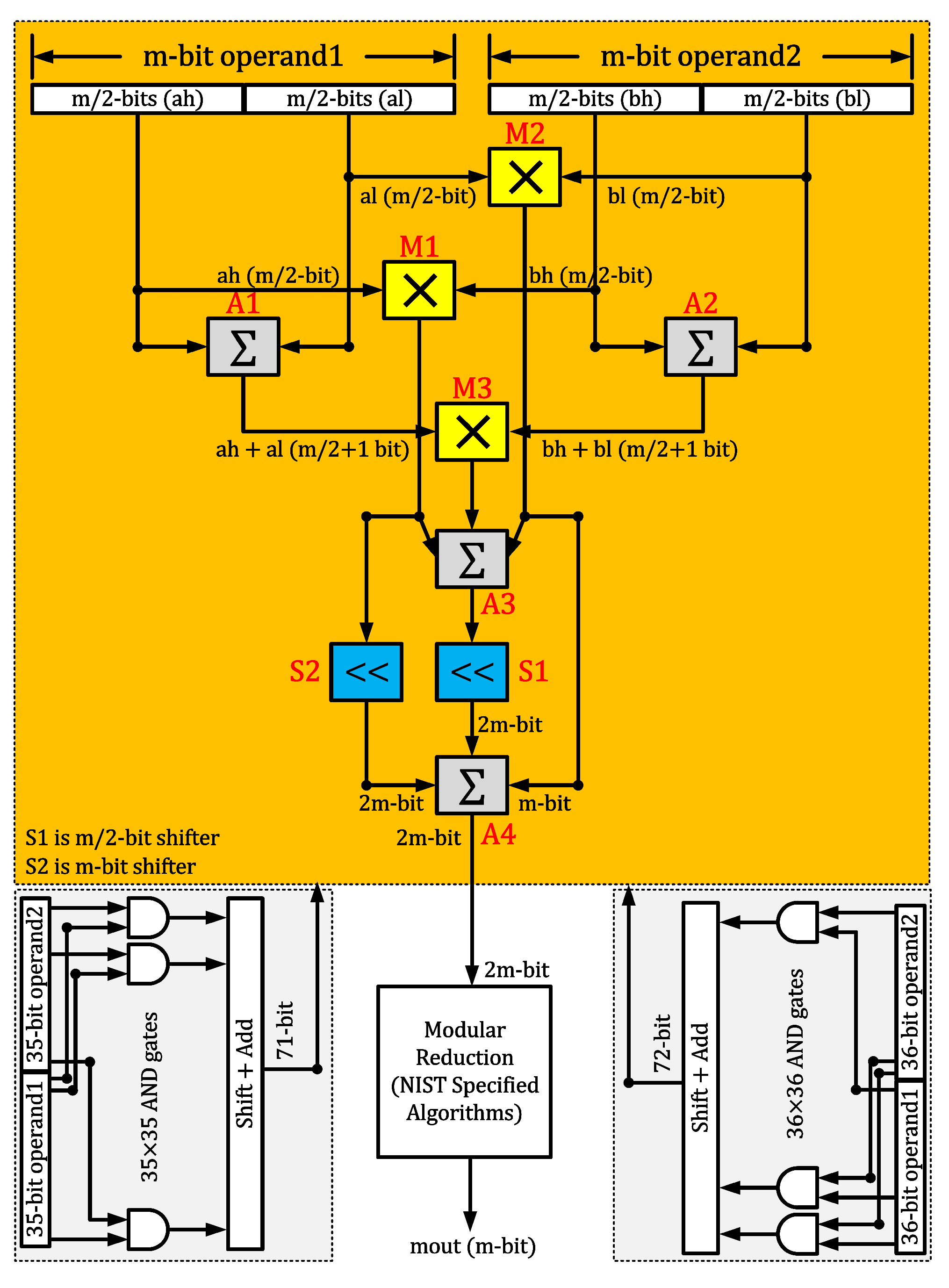
  • Towards the area reduction, we have first proposed a hybrid polynomial multiplier architecture for efficient polynomial multiplications. Subsequently, we have utilized the proposed polynomial multiplier to operate modular square and addition chains of the Itoh-Tsujii algorithm [27] for modular inverse computation. A hybrid approach in our polynomial multiplier design is achieved in two steps: (i) 4-level polynomial splits for multiplying large polynomial operands using a general Karatsuba multiplier and (ii) traditional schoolbook multiplication for smaller polynomial multiplications of length 35 and 36 bits. The details of the hybrid approach are presented in Section 3.3.
  • An efficient finite-state-machine (FSM) based controller is implemented to provide read/write operations from/to utilized memory block. Moreover, the implemented FSM (also) generates the corresponding control signals for the routing networks (i.e., multiplexer(s) and demultiplexer(s)). We have provided the relevant details in Section 3.4.
For validation, the Verilog model of the proposed architecture is simulated and synthesized Vivado IDE tool. We have provided implementation results on Xilinx Virtex 7 FPGA and 65 nm ASIC technologies. The hardware resource utilization of the proposed architecture on ASIC is 30,561 μ m 2 and 36,857 μ m 2 over G F ( 2 409 ) and G F ( 2 571 ) , respectively. Similarly, the FPGA slicesares 4439 and 5683 over G F ( 2 409 ) and G F ( 2 571 ) , respectively. For G F ( 2 409 ) and G F ( 2 571 ) , the clock cycle requirements of the proposed design are 13,903 and 20,551, respectively. The proposed architecture over G F ( 2 409 ) operates on a maximum frequency of 1800 MHz (for ASIC) and 357 MHz (for FPGA). Similarly, the proposed architecture over G F ( 2 571 ) operates on a maximum frequency of 1450 MHz (for ASIC) and 317 MHz (for FPGA). The time for one PM computation on ASIC is 7.72 μ s and 14.17 μ s over G F ( 2 409 ) and G F ( 2 571 ) , respectively. Similarly, the time for one PM computation on FPGA is 38.94 μ s and 64.82 μ s over G F ( 2 409 ) and G F ( 2 571 ) , respectively.
This article is organized as: Section 2 provides the required mathematical knowledge to implement the ECC PM operation. The proposed crypto processor architecture design is described in Section 3. The implementation results and comparisons are given in Section 4. Finally, Section 5 concludes the article.

2. ECC Background

In the case of G F ( 2 m ) field, an affine form of ECC can be represented as a set of points, i.e., x, and y, which obeys the Equation (1) as follows:
E : y 2 + x y = x 3 + a x 2 + b
In Equation (1), x and y are the base elements of the G F ( 2 m ) field. Points a and b represent curve parameters with b 0 . The representation of x and y elements of the G F ( 2 m ) field in a triplet, i.e., X, Y, and Z, is projective coordinates. Thus, for  G F ( 2 m ) field, a Lopez Dahab projective form of Equation (1) is represented in Equation (2). It can be seen in Equation (2) that there are three variables (X, Y and Z). These variables are the projective elements of point P ( X : Y : Z ) , such that Z 0 , a and b are the curve constants with b 0 .
E : Y 2 + X Y Z = X 3 Z + a X 2 Z 2 + b Z 4
The points on the elliptic curve form an additive group. According to the additive group definition, the addition of two elements in a group defines another element in the group. For instance, we have two points, i.e., P and Q, on an elliptic curve. Then a point addition will be R = P + Q , where R will be the resultant point on the curve. Similarly, when both the points on the curve are the same ( P + P = 2 P ) then this is called a point double. These point addition and double operations are needed to compute a point multiplication operation in ECC. Consequently, the addition of k copies of point addition and double determines the ECPM and can be calculated using Equation (3).
Q = k P
The initial point (in Equation (3)) on the curve is P. The resultant point on the curve is Q. Similarly, k is the scalar multiplier. To implement Equation (3), we have several algorithms in the literature such as Double and Add, Lopez Dahab, Montgomery, etc. Comparatively, the Double and Add algorithm is more suitable for the unified models of ECC, such as Edwards, Huff, Twisted Edwards, etc. Similarly, the Lopez Dahab algorithm is a better choice for achieving instruction-level parallelism (i.e., for performance improvements). However, similar instructions for the computation of point addition and double make the Montgomery point multiplication algorithm suitable for the side-channel resistant implementation of ECC. A detailed comparison of various ECPM algorithms is presented in [28]. To summarize, we have used the Montgomery point multiplication algorithm (given in Algorithm 1) in our implementation. It is important to mention that we are not considering the side channel attacks at the design level. In other words, we have implemented only the side channel attack-protected point multiplication algorithm on FPGA and ASIC platforms.
The inputs to Algorithm 1 are an initial point P with x and y coordinates (i.e., x p , and  y p ), and a scalar multiplier k. The bit stream k n 1 , , k 1 , k 0 presents the scalar multiplier. The outputs of the Algorithm 1 are the x and y coordinates of the final point on the ECC curve. For i f and e l s e statements, the corresponding sequence of instructions for point addition and double operations are given in Table 1. Columns one and column two show the point addition information in terms of the sequence of instructions (i.e., I n s t i ) as well as the corresponding operations. Similarly, columns three and column four show the number of instructions (i.e., I n s t i ) as well as the respective finite field operations for point double computations. It can be observed from Table 1 that there are 14 instructions (in total) for point addition and double computations. 6 of these 14 instructions perform finite field multiplications. Similarly, 3 of these 14 instructions perform finite field additions. Finally, the remaining 5 instructions perform finite field squaring.
Algorithm 1: Montgomery PM Algorithm [17,26]
  Input: k = ( k n 1 , , k 1 , k 0 ) with k n 1 = 1 , P = ( x p , y p ) G F ( 2 m )
  Output: Q = ( x q , y q ) = k · P
  1 
Affine to projective conversions: X 1 = x p , Z 1 = 1 , Z 2 = x p 2 and X 2 = x p 4 + b
  2 
PM in projective coordinates:
  3 
for(i from m 2 down to 0)do
Applsci 13 01240 i001
 10 
Reconversion from projective to affine: x q = X 1 Z 1 , y q = x p + ( X 1 Z 1 ) [ ( X 1 + x p × Z 1 ) ( X 2 + x p × Z 2 ) + ( x p 2 + y p ) ( Z 1 × Z 2 ) ] ( x p × Z 1 × Z 2 ) 1 + y p

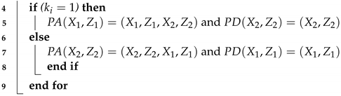
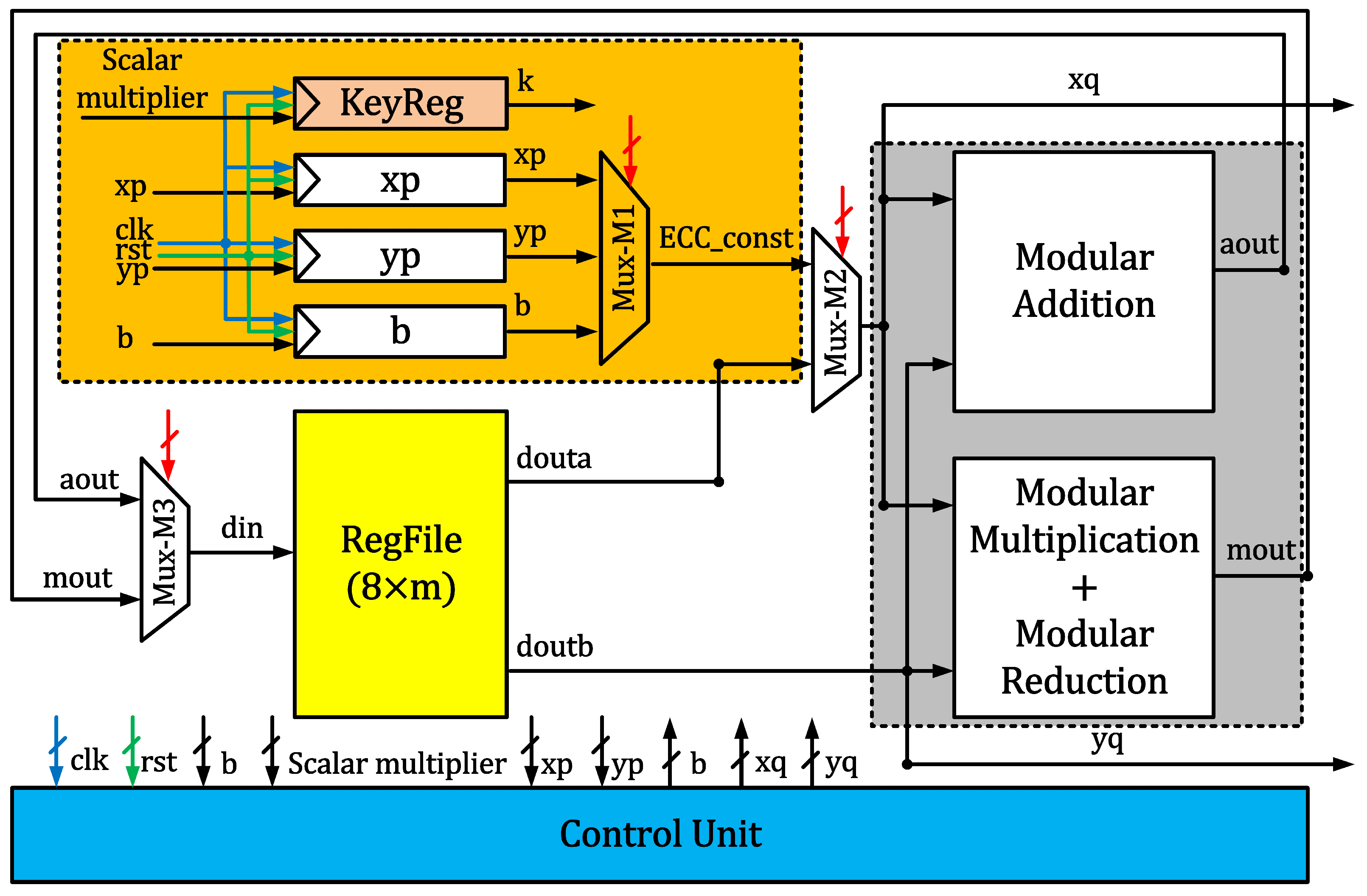
3. Proposed Crypto Processor Architecture

Figure 1 shows the block diagram of our proposed elliptic curve point multiplication architecture. It includes data buffers, a memory block, an arithmetic unit and a control unit. These essential components of our architecture are highlighted with different colors in Figure 1. The data buffers contain input parameters loaded from the outside of the accelerator circuit. The memory block stores the intermediate and the final results after the computation. The arithmetic unit of the proposed accelerator executes the modular operations (addition, square, multiplication and inversion) of layer one of ECC. The control unit generates the corresponding control signals to implement the elliptic-curve PM operation. More insight details are given in the succeeding sections.

3.1. Data Buffers

The orange color in Figure 1 contains four m-bit buffers and a 3 × 1 multiplexer M 1 . The x p and y p buffers contain the x and y coordinate of initial point P. A buffer b holds an m-bit elliptic curve constant. The K e y R e g buffer keeps an m-bit scalar multiplier. Whereas m determines the scalar multiplier length (i.e., k). All these parameters ( x p , y p , b and K e y R e g ) are input to our proposed architecture. The corresponding values for x p , y p and b are selected from a standardized document by NIST.

3.2. RegFile

The yellow color in Figure 1 shows the memory unit. It consists of an 8 × m register array (RegFile). The purpose of this unit is to store the initial, intermediate and final output. It contains two 8 × 1 multiplexers and one 1 × 8 demultiplexer. The objective of (RegFile) multiplexers is to read two m-bit operands for further computations. The demultiplexer is utilized to update the value of the specified register. Finally, for read/write operations, the control signals (shown with red color lines in Figure 1) are generated by the control unit.

3.3. Arithmetic Unit

The gray highlighted portion in Figure 1 shows the arithmetic unit. It contains an m-bit adder and an m-bit multiplier. The adder unit is simply implemented by the bitwise exclusive (OR) operation. For two m-bit operands, m exclusive (OR) gates are needed.

Proposed Hybrid Karatsuba Modular Multiplier

We have performed modular multiplication using a hybrid Karatsuba multiplier. A hybrid approach is achieved by combining Karatsuba and traditional school book multipliers. In order to completely describe our proposed multiplier architecture, we first present the polynomial splits over G F ( 2 571 ) for the Karatsuba multiplier in Figure 2. It can be observed from Figure 2, the input polynomials of length 571-bits are partitioned into two pieces, i.e., 285 and 286. Then, in level two, the split 285-bit polynomial is further divided into two more parts of lengths 142 and 143. We repeat the splitting process until to reach the 35-bit and 36-bit polynomials. Afterward, the multiplication over polynomial lengths of 35-bit and 36-bit is acquired using a traditional schoolbook multiplier. The proposed hybrid modular multiplier architecture is shown in Figure 3.
The orange color portion in Figure 3 determines the Karatsuba multiplication while the gray highlighted regions are for traditional schoolbook multiplication. The proposed hybrid Karatsuba multiplier operates in a way that the schoolbook multiplier performs first to generate the polynomial multiplication result over smaller polynomial lengths. Then, the outputs of the schoolbook multiplier will be transferred to the Karatsuba multiplier to accomplish the required polynomial multiplications over 409 and 571 bits. The area cost of the schoolbook multiplier is 35 AND gates to generate a partial product over 35-bit polynomials. The overall cost includes 35 × 35 (meaning that 35 partial products are needed and the length of each partial product is 35-bits). Some OR gates are needed to generate the resultant product of 71-bits length. Similarly, the area cost of the schoolbook multiplier is 36 AND gates to generate a partial product over 36-bit polynomials. The overall cost will be 36 × 36 . It implies that a total of 36 partial products are needed and each partial product contains a 36-bits length. The final product of 72-bit length is generated using some OR gates. The outputs of schoolbook multipliers is 71 (for 35 × 35 ) and 72 (for 36 × 36 ) bits. These 71 and 72-bit outputs are input to the Karatsuba multiplier for generating multiplications over longer polynomials than 35 and 36 bits.
The Karatsuba multiplier takes two m-bit operands a and b as input and divides them into two m 2 parts. The split parts of polynomial a are a h and a l . Similarly, the split parts of polynomial b are b h and b l . Three multipliers are needed to execute the inner multiplications [29]. The M1 multiplies a h and b h whereas M2 multiplies a l and b l . The multiplier M3 is responsible to multiply the outputs generated after adders, i.e., A1, and A2. Apart from the inner multiplications, the addition of split polynomials is performed. The first adder (i.e., A1) is used to add a h and a l . Similarly, the second adder (i.e., A2) adds the b h and b l polynomials. As seen in Figure 3, the adder A3 adds the multiplication results produced by multipliers M1, M2 and M3. Two shifters, i.e., S1, and S2, are needed to shift polynomials by m 2 and m bit towards the right. Finally, an adder A4 generates the resultant polynomial of length 2 × m and it goes to the reduction block as input to generate an m-bit output. To perform polynomial reduction over G F ( 2 409 ) and G F ( 2 571 ) , we have implemented NIST-specified algorithms as described in Algorithms 2 and 3, respectively. In our work, these reduction algorithms are implemented like combinational circuit because these require only shift and exclusive (OR) operations.
Algorithm 2: NIST reduction over G F ( 2 409 ) [14]
Input: Polynomial, D ( x ) with 2 × m 1 -bit length
Output: Polynomial, D ( x ) with m-bit length
  • f o r ( i f r o m 25 d o w n t o 13 ) d o
      1.1
    T D [ i ]
      1.2
    D [ i 13 ] D [ i 13 ] ( T 7 )
      1.3
    D [ i 12 ] D [ i 12 ] ( T 25 )
      1.4
    D [ i 11 ] D [ i 11 ] ( T 30 )
      1.5
    D [ i 10 ] D [ i 10 ] ( T 2 )
  • T D [ 12 ] 25
  • D [ 0 ] D [ 0 ] T
  • D [ 2 ] D [ 2 ] ( T ! ! 23 )
  • D [ 12 ] D [ 12 ] & 0 x 1 FFFFFF
  • R e t u r n ( D [ 12 ] , , D [ 3 ] , D [ 2 ] , D [ 1 ] , D [ 0 ] )
Algorithm 3: NIST reduction over G F ( 2 571 ) [14]
Input: Polynomial, D ( x ) with 2 × m 1 -bit length
Output: Polynomial, D ( x ) with m-bit length
  • f o r ( i f r o m 35 d o w n t o 18 ) d o
      1.1
    T D [ i ]
      1.2
    D [ i 18 ] D [ i 18 ] ( T 5 ) ( T 7 ) ( T 10 ) ( T 15 )
      1.3
    D [ i 17 ] D [ i 17 ] ( T 27 ) ( T 25 ) ( T 22 ) ( T 17 )
  • T D [ 17 ] 27
  • D [ 0 ] D [ 0 ] T ( T 2 ) ( T 5 ) ( T 10 )
  • D [ 17 ] D [ 17 ] & 0 x 7 FFFFFFF
  • R e t u r n ( D [ 17 ] , , D [ 3 ] , D [ 2 ] , D [ 1 ] , D [ 0 ] )
The reconversion in Algorithm 1 requires modular inversion operation. In the existing literature, we have several algorithms to execute the modular inversion over G F ( 2 409 ) and G F ( 2 571 ) . Our implementation executes the inversion operation using the square version of Itoh-Tsujii algorithm [27]. It requires m 1 squares followed by 10 & 11 multiplications over G F ( 2 409 ) and G F ( 2 571 ) , where m is the operand length. From a hardware implementation perspective, there are two possibilities to implement modular inversion: (1) using a separate square and a multiplier block and (2) using existing hardware resources of a modular multiplier. The first method is inconvenient as it utilizes more hardware resources and consumes more power. The second approach is appealing to save the implementation resources and keep low power consumption of the circuit [15,25,26].
The instructions in Table 1 contain square, multiplication and addition operations. It is important to note that we have used only a single modular multiplier to perform both square and modular multiplications. The square is computed by providing two similar operands as inputs to the multiplier, as described in [26]. Similarly, the Itoh-Tsujii inversion algorithm is implemented using the existing hardware resources of our proposed modular multiplier, as implemented using hardware resources of different multipliers in [25,26]. The proposed multiplier architecture is implemented as combinational logic and it requires only one clock cycle (including reduction) to perform one polynomial square and multiplication.

3.4. Control Unit and Clock Cycles Calculation

An FSM-based dedicated controller is used to implement Algorithm 1 for PM computation. Therefore, during each stage of the FSM, the corresponding read/write signals are generated for the RegFile unit. Moreover, the dedicated controller is (also) responsible to generate the corresponding control signals for routing multiplexers. Using the proposed architecture, the affine to projective conversions of Algorithm 1 take 4 clock cycles. The f o r loop (or point multiplication in projective coordinates) in Algorithm 1 requires 14 instructions of Table 1. Out of these 14 instructions, 7 are for point addition and the other 7 are for point double. All these 14 instructions require addition, multiplication and square operations. Therefore, the computational cost of the f o r loop of Algorithm 1 is 14 ( m 2 ) clock cycles, where m is the implemented key length.
For G F ( 2 409 ) and G F ( 2 571 ) , the clock cycle requirement is 5698 and 7966, respectively. The reconversions from projective to affine of Algorithm 1 require two modular inversion operations. As we have mentioned before, the inversion needs m 1 squares followed by 10 and 11 field multiplications. In addition, the cycle count for each square and multiplication computation is one. Therefore, the total cycle count for each inversion over G F ( 2 409 ) and G F ( 2 571 ) is 4080 and 6270 respectively. The total cost for inversion (in terms of clock cycles) over G F ( 2 409 ) and G F ( 2 571 ) is 8160 and 12,540 respectively. The 41 cycles are needed to calculate the remaining computations of reconversion in Algorithm 1. Consequently, the total number of clock cycles (to implement Algorithm 1 over G F ( 2 409 ) and G F ( 2 571 ) ) are 13,903 and 20,551 respectively.

4. Implementation Results and Performance Comparison

The register-transfer-level (RTL) implementation of our proposed crypto processor architecture over G F ( 2 409 ) and G F ( 2 571 ) is implemented in Verilog HDL using a Vivado IDE. For targeted binary field lengths, i.e., 409 and 571, the initial point P and a curve constant value b as inputs are selected from NIST standardized document [13]. Therefore, we describe implementation results and our comparison to state-of-the-art in Section 4.1 and Section 4.2, respectively.

4.1. Results

The implementation results on FPGA and ASIC devices are shown in Table 2 and Table 3, respectively. For FPGA implementations, we have provided results on Xilinx Virtex 7 (a modern 28 nm technology) device. Moreover, the synthesis results for ASIC is provided on a commercial 65 nm process technology. Concerning Table 2, the targeted field length m is shown in column one. Columns two to four provide the area results in slices, look-up-tables (LUTs) and flip-flops (FFs). The timing information in terms of clock cycles, frequency (Freq), latency and throughput (Thrpt) are given in columns five to eight. A figure-of-merit (FoM) is defined in terms of a ratio of throughput over slices to evaluate the performance of the proposed crypto processor. Similarly, considering Table 3, the targeted field length m is shown in column one. Column two shows the area (in mm 2 ) results. The timing information in terms of clock cycles, frequency (Freq), latency and throughput (Thrpt) are given in columns three to six. A FoM is also defined in terms of a ratio of throughput over area. For FPGA and ASIC implementations, the area (slices, LUTs, FFs for FPGA) and frequency values are collected from the synthesis tool (Vivado IDE for FPGA and Cadence Genus for ASIC). The clock cycles calculation is already described in Section 3.4. Similarly, the latency and throughput values are calculated using Equation (4) and Equation (5), respectively. Finally, the figure-of-merit values are calculated using Equation (6).
L a t e n c y ( μ s ) = C l o c k c y c l e s C l o c k f r e q u e n c y ( MHz )
T h r o u g h p u t ( T h r p t ) = 1 L a t e n c y ( μ s ) = 10 6 L a t e n c y
F o M = T h r o u g h p u t ( T h r p t ) A r e a ( s l i c e s f o r F P G A )
Comparison of G F ( 2 409 ) & G F ( 2 571 ) on FPGA.Table 2 demonstrates that the increase in the field length increases hardware resources (slices, LUTs and FFs). For example, the slices, LUTs and FFs for G F ( 2 409 ) field are 0.78 (ratio of 4439 over 5683), 0.87 (ratio of 12,568 over 14,356) and 0.69 (ratio of 4129 over 5961) times lower than G F ( 2 571 ) field. Similarly, the computational cost to execute one PM operation on G F ( 2 409 ) field is 0.67 (ratio of 13,903 over 20,551) times lower than G F ( 2 571 ) field. Moreover, on a modern Virtex 7 FPGA device, our proposed architecture can operate on a maximum 357 MHz and 317 MHz clock frequency over G F ( 2 409 ) and G F ( 2 571 ) fields, respectively. As for as the computational cost for one PM execution is concerned, our proposed architecture over G F ( 2 409 ) and G F ( 2 571 ) require 38.94 μ s and 64.82 μ s, respectively. This indicates that the 0.71 (ratio of 409 over 571) times increase in the field length (i.e., from G F ( 2 409 ) to G F ( 2 571 ) ) results in 0.60 (ratio of 38.94 over 64.82) times increase in computation time. If we calculate the ratio of increase in the field length (0.71) with the increase in computation time (0.60), the proposed accelerator architecture over a larger G F ( 2 571 ) field length is more efficient than the architecture over G F ( 2 409 ) field. As shown in column eight of Table 2, the throughput of our proposed accelerator design over G F ( 2 409 ) and G F ( 2 571 ) is 25.68 kbps and 15.42 kbs, respectively. Concerning our defined FoM for comparison, the last column of Table 2 shows that the proposed accelerator architecture over G F ( 2 409 ) is more efficient than G F ( 2 571 ) field. One of the reasons is lower field length (i.e., 409). The lower field length utilizes lower hardware resources and takes lower computational time. Thus, the ratio of throughput over slices results in a higher value for lower field length.
Comparison of G F ( 2 409 ) & G F ( 2 571 ) on ASIC. Similar to FPGA results, Table 3 shows that the increase in the field length increases area. For instance, the area for G F ( 2 409 ) field are 0.82 (ratio of 30,561 over 36,857) times lower than G F ( 2 571 ) field. Moreover, on 65 nm process technology, our proposed architecture can operate on a maximum 1800 MHz and 1450 MHz clock frequency over G F ( 2 409 ) and G F ( 2 571 ) fields, respectively. As for as the computational cost for one PM execution is concerned, our proposed architecture over G F ( 2 409 ) and G F ( 2 571 ) require 7.72 μ s and 14.17 μ s, respectively. This indicates that the 0.71 (ratio of 409 over 571) times increase in the field length (i.e., from G F ( 2 409 ) to G F ( 2 571 ) ) results in 0.54 (ratio of 7.72 over 14.17) times increase in computation time. As shown in column six of Table 3, the throughput of our proposed accelerator design over G F ( 2 409 ) and G F ( 2 571 ) is 129.53 kbps and 70.57 kbs, respectively. When we consider the defined FoM for comparison, the last column of Table 3 shows that the proposed accelerator architecture over G F ( 2 409 ) is more efficient than G F ( 2 571 ) field. The reason is lower field length (i.e., 409). The lower field length utilizes lower hardware resources and takes lower computational time. Hence, the ratio of throughput over area results in a higher value for lower field length.
Comparison to FPGA and ASIC results. As expected, the performance of our proposed architecture on ASIC is more efficient as compared to the FPGA implementations. The area comparison is not possible to provide. However, the frequency achieved on ASIC over G F ( 2 409 ) and G F ( 2 571 ) is 5.02 (ratio of 1800 with 357) and 4.57 (ratio of 1450 with 317) times higher as compared to FPGA. Similarly, the latency calculated for ASIC over G F ( 2 409 ) and G F ( 2 571 ) is 5.04 (ratio of 38.94 with 7.72) and 4.57 (ratio of 64.82 with 14.17) times lower than compared FPGA. The computational cost of our proposed architecture in latency can be reduced by using pipeline registers after each Karatsuba split, shown in Figure 2. If we consider the throughput and FoM values, Table 2 and Table 3 reveal that the ASIC implementations on 65 nm technology are more efficient as compared to the modern 28 nm technology on FPGA.

4.2. Comparison to State of the Art

The comparison to state-of-the-art architectures is shown in Table 4. Column one gives the reference design and publication year (in form of Ref/Year). The utilized field length m is illustrated in column two. The implementation device is presented in column three. Columns four and five show the hardware resources in FPGA slices and LUTs. The last three columns provide the timing information in clock cycles, operational frequency and latency.
Comparison to Weierstrass model of ECC. As compared to [15], our proposed architecture utilizes 2.67 and 3.50 times lower slices on Virtex 7 FPGA device over G F ( 2 409 ) and G F ( 2 571 ) , respectively. The cause to achieve higher resource utilization in [15] is the parallel computation of Frobenius maps and point additions while in our work, we use a non-pipelined Karatsuba multiplier. Note that the clock cycles and frequency comparison are not feasible as the particular information is not given. On the other hand, the operation rescheduling for PA and PD computations result in lower latency values (9.50 over G F ( 2 409 ) and 18.51 over G F ( 2 571 ) ) as compared to our work (39.83 over G F ( 2 409 ) and 66.08 over G F ( 2 571 ) ). There is always a tradeoff between hardware resources and computational time (i.e., latency).
Concerning [23,29,31], the bit-serial and digit-serial multipliers are practical to reduce hardware resources while bit-parallel and digit-parallel multipliers are more convenient to reduce computational cost with area and power overheads. Therefore, over G F ( 2 409 ) and G F ( 2 571 ) , the use of a segmented digit-serial multiplier in [17] results in 1.49 and 2.23 times higher FPGA slices as compared to our proposed architecture where we employed a hybrid bit-parallel Karatsuba multiplier architecture of Figure 3. The clock cycle comparison is not possible as the relevant information is not described in the work of [17]. If we compare the circuit frequency, our architecture is 1.10 and 1.24 times more efficient. The computational cost of our proposed architecture is comparatively 0.82 and 0.87 times higher. Again, we remind the reader that there is always a tradeoff between the area and processing time.
On Virtex 6 FPGA, we provide the area comparison of our work in terms of LUTs with the unified architecture of [19] as the information of the FPGA slices is not reported. Comparatively, our architecture utilizes 7.97 and 6.89 times lower FPGA LUTs over G F ( 2 409 ) and G F ( 2 571 ) . The reason for the use of lower resources in our work is that we proposed dedicated designs for G F ( 2 409 ) and G F ( 2 571 ) fields while in [19] a unified ECC architecture is proposed to implement binary field lengths from G F ( 2 233 ) to G F ( 2 571 ) . As shown in Table 4, the clock cycles utilized in [19] are lower as compared to our work but we achieved higher operational frequency (210 for G F ( 2 409 ) and 170 for G F ( 2 571 ) ). The average sum of frequency achieved for G F ( 2 409 ) and G F ( 2 571 ) is 190 MHz (210 MHz + 170 MHz then divided by 2). Comparatively, our average frequency of two dedicated designs is 1.40 times higher as compared to the frequency (135 MHz) achieved for the unified design of [19]. As we are utilizing the lower hardware resources but our design takes more processing time.
As compared to the 6CC-6CC architecture of [16], our hybrid Karatsuba multiplier-based ECPM design takes 5.51 (ratio of 80,970 over 14,687) times lower FPGA LUTs. Similarly, as shown in Table 4, our architecture can operate on maximum 311 MHz while the design of [16] can operate on 274 MHz which is comparatively 1.13 (ratio of 311 over 274) times lower than our work. But, the latency values calculated for [16] are lower than our work (shown in Table 4). There is always a tradeoff.
Comparison to Edward model of ECC. As shown in Table 4, the Edward model of ECC on G F ( p ) and G F ( 2 m ) field lengths are implemented in [20,21,22,23,30]. These Edward curve implementations utilize 256-bit and 233-bit field lengths. But in our work, we utilize only the higher field lengths of 409 and 571. In short, due to different field lengths, a fair comparison is impossible to provide. As seen in Table 4, for higher field lengths of 409-bit and 571-bit, our architectures on Virtex 6 and Virtex 7 achieves higher operational frequency as compared to Edward designs of [20,21,22,23,30]. Similarly, as compared to [20,21,22,30], our architectures take lower computational time (i.e., latency) on Virtex 6 and Virtex 7 FPGA devices. The design of [23] is more efficient as compared to our work in terms of latency as their architecture utilizes 233-bit field length while in our work we use 409 and 571 bits field length. The area comparison is non-trivial as lower field lengths are targeted in designs of [20,21,22,23,30] when compared to our work. Consequently, the proposed large field length designs of this work are competent for recent Edward-based FPGA solutions.
Comparison to Huff model of ECC.Table 4 provides that the Huff model of ECC on G F ( 2 233 ) field length is implemented in [24,25]. Due to higher field lengths (409-bit and 571-bit) in our work, a reasonable comparison is impossible to provide. On Virtex 7 FPGA, the 4-stage pipeline designs of [24,25] over G F ( 2 233 ) takes 1.22 (ratio of 7123 over 5797) and 1.21 (ratio of 7017 over 5797) times higher FPGA slices as compared to our non-pipelined architecture over G F ( 2 571 ) . On a similar Virtex 7 device, the comparison to latency reveals that the proposed architecture over G F ( 2 571 ) is more efficient than the design of [25] over G F ( 2 233 ) . As the field lengths are different, the design of [24] over G F ( 2 233 ) takes 2.19 (ratio of 66.08 over 30.08) times lower computational time as compared to our Virtex 7 implementation of G F ( 2 571 ) .

5. Conclusions

This article has presented a novel elliptic curve cryptographic processor over G F ( 2 409 ) and G F ( 2 571 ) using Lopez-Dahab projective point arithmetic operations. The critical feature of this work is a hybrid Karatsuba multiplier of 4-split polynomials to multiply two polynomial multiplications. A hybrid multiplier is implemented using a general Karatsuba and traditional schoolbook multiplication approaches. For low hardware resource utilizations, the proposed multiplier design is employed to implement the modular squares and addition chains of the Itoh-Tsujii algorithm for inverse computations. On Xilinx Virtex 7 FPGA device, the number of the required slices is 4439 and 5683 over ( 2 409 ) and G F ( 2 571 ) , respectively. Similarly, on ASIC 65nm process technology, the core size is 30,561 μ m 2 and 36,857 μ m 2 for G F ( 2 409 ) and G F ( 2 571 ) , respectively. The comparison to existing designs in the literature shows that the proposed architecture utilizes less area and provides competent performance for PM computation. Therefore, the proposed design is an alternate for area-constrained cryptosystems.

Author Contributions

Conceptualization, M.R. and M.A.; methodology, M.R. and M.Y.I.Z.; software, N.K. and M.A.; validation, M.R. and M.A.; formal analysis, M.R. and N.K.; investigation, M.A. and M.R.; resources, M.R. and N.K.; data curation, O.S.S.; writing—original draft preparation, M.R. and M.H.S.; writing—review and editing, M.R. and M.Y.I.Z.; visualization, O.S.S.; supervision, M.R. and M.Y.I.Z. All authors have read and agreed to the published version of the manuscript.

Funding

The authors would like to thank the Deanship of Scientific Research at Umm Al-Qura University for supporting this work by Grant Code: (22UQU4320020DSR01).

Institutional Review Board Statement

Not applicable.

Informed Consent Statement

Not applicable.

Data Availability Statement

Not applicable.

Conflicts of Interest

The authors declare that they have no conflict of interest.

References

  1. Miller, V.S. Use of Elliptic Curves in Cryptography. In Proceedings of the Advances in Cryptology—CRYPTO’85 Proceedings; Williams, H.C., Ed.; Springer: Berlin/Heidelberg, Germany, 1986; pp. 417–426. [Google Scholar]
  2. Rivest, R.L.; Shamir, A.; Adleman, L. A method for obtaining digital signatures and public-key cryptosystems. Commun. ACM 1978, 21, 120–126. [Google Scholar] [CrossRef] [Green Version]
  3. Sinha Roy, S.; Basso, A. High-speed Instruction-set Coprocessor for Lattice-based Key Encapsulation Mechanism: Saber in Hardware. IACR Trans. Cryptogr. Hardw. Embed. Syst. 2020, 2020, 443–466. [Google Scholar] [CrossRef]
  4. Imran, M.; Almeida, F.; Raik, J.; Basso, A.; Roy, S.S.; Pagliarini, S. Design Space Exploration of SABER in 65 nm ASIC. In Proceedings of the 5th Workshop on Attacks and Solutions in Hardware Security, Virtual Event, 19 November 2021; Association for Computing Machinery: New York, NY, USA, 2021; pp. 85–90. [Google Scholar] [CrossRef]
  5. NIST. PQC Standardization Process: Announcing Four Candidates to be Standardized, Plus Fourth Round Candidates. Available online: https://csrc.nist.gov/News/2022/pqc-candidates-to-be-standardized-and-round-4 (accessed on 11 August 2022).
  6. Kumar, K.A.; Krishna, A.V.N.; Chatrapati, K.S. New secure routing protocol with elliptic curve cryptography for military heterogeneous wireless sensor networks. J. Inf. Optim. Sci. 2017, 38, 341–365. [Google Scholar] [CrossRef]
  7. Gulen, U.; Baktir, S. Elliptic Curve Cryptography for Wireless Sensor Networks Using the Number Theoretic Transform. Sensors 2020, 20, 1507. [Google Scholar] [CrossRef] [PubMed] [Green Version]
  8. Noori, D.; Shakeri, H.; Niazi, T.M. Scalable, efficient, and secure RFID with elliptic curve cryptosystem for Internet of Things in healthcare environment. EURASIP J. Inf. Secur. 2020, 2020, 13. [Google Scholar] [CrossRef]
  9. Calderoni, L.; Maio, D. Lightweight Security Settings in RFID Technology for Smart Agri-Food Certification. In Proceedings of the 2020 IEEE International Conference on Smart Computing (SMARTCOMP), Bologna, Italy, 22–25 June 2020; pp. 226–231. [Google Scholar] [CrossRef]
  10. Singh, R.; Miglani, S. Efficient and secure message transfer in VANET. In Proceedings of the 2016 International Conference on Inventive Computation Technologies (ICICT), Coimbatore, India, 26–27 August 2016; Volume 2, pp. 1–5. [Google Scholar] [CrossRef]
  11. Chavhan, S.; Doriya, R. Secured Map Building using Elliptic Curve Integrated Encryption Scheme and Kerberos for Cloud-based Robots. In Proceedings of the 2020 Fourth International Conference on Computing Methodologies and Communication (ICCMC), Erode, India, 11–13 March 2020; pp. 157–164. [Google Scholar] [CrossRef]
  12. Malina, L.; Dzurenda, P.; Ricci, S.; Hajny, J.; Srivastava, G.; Matulevičius, R.; Affia, A.A.O.; Laurent, M.; Sultan, N.H.; Tang, Q. Post-Quantum Era Privacy Protection for Intelligent Infrastructures. IEEE Access 2021, 9, 36038–36077. [Google Scholar] [CrossRef]
  13. NIST. Recommended Elliptic Curves for Federal Government Use (1999). Available online: https://csrc.nist.gov/csrc/media/publications/fips/186/2/archive/2000-01-27/documents/fips186-2.pdf (accessed on 5 January 2023).
  14. Hankerson, D.; Menezes, A.J.; Vanstone, S. Guide to Elliptic Curve Cryptography; Springer: New York, NY, USA, 2004; pp. 1–311. Available online: https://link.springer.com/book/10.1007/b97644 (accessed on 5 January 2023).
  15. Li, L.; Li, S. High-Performance Pipelined Architecture of Point Multiplication on Koblitz Curves. IEEE Trans. Circuits Syst. II Express Briefs 2018, 65, 1723–1727. [Google Scholar] [CrossRef]
  16. Li, J.; Wang, W.; Zhang, J.; Luo, Y.; Ren, S. Innovative Dual-Binary-Field Architecture for Point Multiplication of Elliptic Curve Cryptography. IEEE Access 2021, 9, 12405–12419. [Google Scholar] [CrossRef]
  17. Khan, Z.U.A.; Benaissa, M. Throughput/Area-efficient ECC Processor Using Montgomery Point Multiplication on FPGA. IEEE Trans. Circuits Syst. II Express Briefs 2015, 62, 1078–1082. [Google Scholar] [CrossRef]
  18. Imran, M.; Pagliarini, S.; Rashid, M. An Area Aware Accelerator for Elliptic Curve Point Multiplication. In Proceedings of the 2020 27th IEEE International Conference on Electronics, Circuits and Systems (ICECS), Glasgow, UK, 23–25 November 2020; pp. 1–4. [Google Scholar] [CrossRef]
  19. Zhao, X.; Li, B.; Zhang, L.; Wang, Y.; Zhang, Y.; Chen, R. FPGA Implementation of High-Efficiency ECC Point Multiplication Circuit. Electronics 2021, 10, 1252. [Google Scholar] [CrossRef]
  20. Islam, M.M.; Hossain, M.S.; Hasan, M.K.; Shahjalal, M.; Jang, Y.M. Design and Implementation of High-Performance ECC Processor with Unified Point Addition on Twisted Edwards Curve. Sensors 2020, 20, 5148. [Google Scholar] [CrossRef]
  21. Islam, M.M.; Hossain, M.S.; Hasan, M.K.; Shahjalal, M.; Jang, Y. FPGA Implementation of High-Speed Area-Efficient Processor for Elliptic Curve Point Multiplication Over Prime Field. IEEE Access 2019, 7, 178811–178826. [Google Scholar] [CrossRef]
  22. Lara-Nino, C.A.; Diaz-Perez, A.; Morales-Sandoval, M. Lightweight elliptic curve cryptography accelerator for internet of things applications. Ad Hoc Netw. 2020, 103, 102159. [Google Scholar] [CrossRef]
  23. Sajid, A.; Rashid, M.; Imran, M.; Jafri, A.R. A Low-Complexity Edward-Curve Point Multiplication Architecture. Electronics 2021, 10, 1080. [Google Scholar] [CrossRef]
  24. Rashid, M.; Imran, M.; Jafri, A.R.; Mehmood, Z. A 4-Stage Pipelined Architecture for Point Multiplication of Binary Huff Curves. J. Circuits Syst. Comput. 2020, 29, 2050179. [Google Scholar] [CrossRef]
  25. Rashid, M.; Imran, M.; Kashif, M.; Sajid, A. An Optimized Architecture for Binary Huff Curves With Improved Security. IEEE Access 2021, 9, 88498–88511. [Google Scholar] [CrossRef]
  26. Imran, M.; Rashid, M.; Jafri, A.R.; Kashif, M. Throughput/area optimised pipelined architecture for elliptic curve crypto processor. IET Comput. Digit. Tech. 2019, 13, 361–368. [Google Scholar] [CrossRef] [Green Version]
  27. Itoh, T.; Tsujii, S. A fast algorithm for computing multiplicative inverses in GF (2m) using normal bases. Inf. Comput. 1988, 78, 171–177. [Google Scholar] [CrossRef] [Green Version]
  28. Rashid, M.; Imran, M.; Jafri, A.R.; Al-Somani, T.F. Flexible Architectures for Cryptographic Algorithms — A Systematic Literature Review. J. Circuits, Syst. Comput. 2019, 28, 1930003. [Google Scholar] [CrossRef]
  29. Imran, M.; Abideen, Z.U.; Pagliarini, S. An Open-source Library of Large Integer Polynomial Multipliers. In Proceedings of the 2021 24th International Symposium on Design and Diagnostics of Electronic Circuits & Systems (DDECS), Vienna, Austria, 7–9 April 2021; pp. 145–150. [Google Scholar] [CrossRef]
  30. Mehrabi, M.A.; Doche, C. Low-Cost, Low-Power FPGA Implementation of ED25519 and CURVE25519 Point Multiplication. Information 2019, 10, 285. [Google Scholar] [CrossRef] [Green Version]
  31. Imran, M.; Rashid, M. Architectural review of polynomial bases finite field multipliers over GF(2m). In Proceedings of the 2017 International Conference on Communication, Computing and Digital Systems (C-CODE), Islamabad, Pakistan, 8–9 March 2017; pp. 331–336. [Google Scholar] [CrossRef]
Figure 1. Block diagram of our large field-size elliptic curve cryptographic processor in G F ( 2 m ) .
Applsci 13 01240 g001
Figure 2. Polynomial splits of a Karatsuba modular multiplier over G F ( 2 571 ) .
Applsci 13 01240 g002
Figure 3. Proposed Karatsuba modular multiplier.
Applsci 13 01240 g003
Table 1. Point addition and double instructions.
Inst i Point Addition ( PA )Inst i Point Double ( PD )
I n s t 1 Z 1 = X 2 × Z 1 I n s t 1 Z 2 = Z 2 2
I n s t 2 X 1 = X 1 × Z 2 I n s t 2 T 1 = Z 2 2
I n s t 3 T 1 = X 1 + Z 1 I n s t 3 T 1 = b × T 1
I n s t 4 X 1 = X 1 × Z 1 I n s t 4 X 2 = X 2 2
I n s t 5 Z 1 = T 1 2 I n s t 5 Z 2 = X 2 × Z 2
I n s t 6 T 1 = x p × Z 1 I n s t 6 X 2 = X 2 2
I n s t 7 X 1 = X 1 + T 1 I n s t 7 X 2 = X 2 + T 1
Table 2. Implementation results on Xilinx (Virtex 7) FPGA.
mSlicesLUTsFFsClock CyclesFreq (MHz)Latency ( μ s)ThrptFoM
409443912,568412913,90335738.9425.68 kbps5.78
571568314,356596120,55131764.8215.42 kbps1.07
Table 3. Synthesis results on (65 nm) ASIC.
mArea ( μ m 2 )Clock CyclesFreq (MHz)Latency ( μ s)ThrptFoM
40930,56113,90318007.72129.53 kbps4238.40
57136,85720,551145014.1770.57 kbps1914.69
Table 4. Comparison to related PM architectures.
Ref/YearmDeviceSlicesLUTsCCsFreq (MHz)Latency ( μ s)
Implementations of Weierstrass model of ECC
[15]/2018409Virtex 712,290NANANA9.50
[17]/2015409Virtex 7688820,881NA31632.72
[19]/2021409Virtex 6NA116,241578413541.36
[15]/2018571Virtex 720,291NANANA18.51
[17]/2015571Virtex 712,96538,547NA25057.61
[19]/2021571Virtex 6NA116,241762813556.50
[16]/2021571Virtex 7NA80,970NA27412.55
Implementations of Edward model of ECC
[20]/2020256Virtex 66600NANA932130
[21]/2019256Virtex 78873NA262,6501781480
[22]/2020233Virtex 612453878NA1076720
[23]/2021233Virtex 7266224,727324417918.10
[30]/2019CURVE25519ZYNQ 7000NA12.95kNA137280.64
Implementations of Huff model of ECC
[25]/2021233Virtex 77123NA15,49518882.4
[24]/2020233Virtex 77017NA13,05743430.08
This work409Virtex 6643914,57813,90321066.20
This work571Virtex 6723716,85620,551170120.88
This work409Virtex 7459612,84513,90334939.83
This work571Virtex 7579714,68720,55131166.08
Disclaimer/Publisher’s Note: The statements, opinions and data contained in all publications are solely those of the individual author(s) and contributor(s) and not of MDPI and/or the editor(s). MDPI and/or the editor(s) disclaim responsibility for any injury to people or property resulting from any ideas, methods, instructions or products referred to in the content.

