Abstract
A novel multi-beam photonic receiver with a variable beam count has been proposed. The reconfigurable characteristic of the system is enabled with the variable splitters and optical switch arrays. According to the number of beams it is due to receive, the splitter with suitable ports is chosen to split by controlling the optical switch in order to configure the optical path. After splitting, the multi-wavelength optical carriers are sent to the wavelength division multiplexer to combine and complete the multi-beamforming process. Two structures have been designed to realize the reconfigurable function, while the optimized structure is proved by using several benchmarks for comparison. The operation step of the reconfigurable multi-beam receiver is then given. The first simulations validate that the proposed architecture can dynamically receive the multi-beam with a variable number by reconfiguring the state of the optical switch. The second simulation of the influence on the received beam pattern was performed under a different amplitude and phase inconsistency random values. The results show that the amplitude and phase inconsistency will decline the quality of the multi-beam. When the amplitude and phase inconsistency are within limits, the difference in the optical path within the outputs must be balanced and compensated during the proposed system’s fabrication and deployment.
1. Introduction
The beamformer will become the key component in future telecommunications with the deployment of mobile broadband, the large-scale Internet-of-Things (IoT), self-driving cars, telemedicine, and cloud-gaming [1]. To better offer such services, the next generation of wireless communication will need to expand the spectrum and explore a new dimension: spatial-division multiplexing (SDM). With SDM, each user may access the entire spectrum without interference. Thus, implanting SDM is becoming a hot topic in research. The design of the broadband antennas [2] and the multi-beamforming [3] to support the SDM are two promising directions. Moreover, using the photonic beamformer as the broadband multi-beam signal processing has its own advantages and huge potential. The beamformer built by microwave photonics technology inherits the advantage of microwave photonics, such as low loss, wide bandwidth, and immunity to electromagnetic interference [4,5]. Realizing the true-time delay line in optical circuits is simpler than in electronic circuits [6,7,8,9]. The beamformer based on the true-time delay can effectively eliminate the beam-squint effect and is more suitable for the next generation of wireless communications. Furthermore, optical beamformers can easily form multi-beams by incorporating wavelength division multiplexing (WDM) because the splitting in the optical domain is not limited by the signal bandwidth.
Numerous studies have reported on the optical beamformer architecture to support multi-beam antennas [10,11,12,13,14,15,16]. Four independent beams with eight scan angles were realized using a large port-count demultiplexer and fast-tunable lasers [12]. The beamforming networks built as the optical Blass matrix architecture in phase shifters and Mach–Zehnder interferometers to generate three beams simultaneously pointing in different directions were realized [13]. The whole array was divided into multiple subarrays, and each subarray was used to form a beam that also achieves the one array transmitting multi-beam simultaneously. But it is not multi-beamforming in the strict sense [14]. Recently, using programmable photonics processors to manipulate the WDM optical signals to achieve multi-beam antennas has been reported [15].
However, these architectures only achieved the multi-beam architecture in which the number of beams is fixed. this means that the system affords constant optical power overhead and cannot adapt to the various scenarios in future communications. For example, when the number of users or the distance between the base station and the user is changed, the above structure may not offer high-quality services. To overcome this shortcoming, designing a multi-beamforming architecture in which the number of beams is reconfigurable is necessary.
In this manuscript, we proposed a multi-beamformer architecture with a variable beam-count by introducing the reconfigurable optical switch and the variable splitter into a conventional space multiplexing multi-beam architecture. We reconfigured the state of the switches dynamically to split the optical carrier according to the needs of current scenarios. This method focuses the optical energy into the beams that need to be received and improves the system’s energy efficiency. This manuscript includes the process of designing and optimizing the beamformer architecture, followed by theoretical analysis and multi-beam pattern simulation. The numerical simulation result confirms that the system with a variable beam-count has high energy efficiency and adapts to future communications smartly.
2. System Architecture
The conventional multi-beam receiver based on the true-time delay line is described in Figure 1. The signal received by every antenna element (AE) is modulated on the optical carrier with different and independent wavelengths; the wavelength spacings are followed with ITU G.692 standard [17] to avoid interference. The optical carrier with the signal is next sent to the splitter and divided into multiple duplications with an equal number to the number of the system-supporting received beams. After splitting, each duplication passes the individual optical delay line (ODL) and is enabled with delay weighting. The multi-wavelength signals are sent to the WDM multiplexer to couple together as a group, each containing different wavelengths. Finally, the photoelectric conversion is completed at the photonic detector, and the signal in the electronic domain is obtained. The ODL in the structure was demonstrated earlier in [6]. The true-time delay value offered by the ODL is independent of the optical carrier’s wavelength and has a long range. The number of the received beam is fixed. Let us assume that the numbers of the AEs and the received beam in the analyzed system are N and M, respectively. In the conventional architecture, the signal received by one AE is passively split into M parts, each corresponding to one beam. When the system receives only one beam, the optical power in the remaining unused ports will be wasted. Meanwhile, the energy in the current used port remains at a low level.
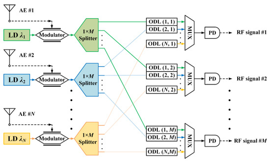
Figure 1.
Illustration of the conventional multi-beam receiver. LD: laser diode; ODL: optical delay line; MUX: multiplexer; PD: photoelectric detector.
To surmount the above demerit, we propose introducing the switch before the splitter part to realize a reconfigurable multi-beamformer, as shown in Figure 2.
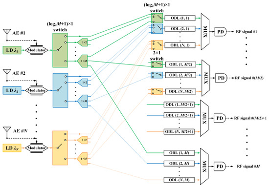
Figure 2.
Illustration of structure DP (descending-precedence).
Two reconfigurable parts of the switch are added to the conventional multi-beam structure. The splitter is expanded, and each one has different output ports. But this new structure still has the same number of lasers, modulators, ODL, MUX, and PD.
The function of the switch before the splitter is to choose the suitable splitter and reconfigure the system’s working mode; we named it the mode-switch. The proposed structure only supports the working mode when the number of the beam is any exponential power multiple of 2, and the working mode can be denoted with the sequence number m, m = 1, 2, 4, …, 2n, …, M, n∈Z. When m = 1, the system works on a single-beam mode; similarly, when m = 2, the system works on dual-beam mode, and so on and so forth. The switch was also applied before true-time delay units instead of the combiner to decrease the insertion loss, named the combiner-switch. The precedence of beam ports is allotted in descending numerical order in Figure 2. Output 1 works for the single-beam mode, dual-beam mode, and up until the M-beam mode, while the total number of the mode is log2(M) + 1. Output 2 works for the dual-beam mode to the M-beam mode. The number of modes supported in output 2 is less 1 than output 1. As for the n-th output, when n ≤ M/2, the output n works for the 2⎣log2(n)⎦ beam mode to the M-beam mode; when n > M/2, the output n only works for the M-beam mode. Inside, ⎣·⎦ denotes a round-up to an integer. For convenience, as described in the following, the structure in Figure 2 is named the structure descending-precedence (structure DP).
The asymmetrical switch will occur in the structure DP when we build the odd-ports multi-stage switch in the fundamental block (1 × 2 switch). The asymmetrical switch may cause inconsistency in amplitude and phase. The optimized structure, which is designed to keep the consistency, is presented in Figure 3. In the optimal structure, output 1 is used for the single-beam mode or the M-beam receive mode, and outputs 2 and 3 are used for the dual-beam or M-beam receive mode. Thus, any output n, except for the M-th port, only works for two modes. One is the M-beam mode, and the other is the 2⎡log2(n)⎤ mode. ⎡·⎤ denotes the round-down to an integer. Therefore, we use the basic 1 × 2 switch instead of the multi-stages switch to avoid causing amplitude and phase inconsistency. Compared to the structure DP, the outputs in structure in Figure 3 have almost equal precedence, and we named it the equal-precedence (structure EP) for convenience.
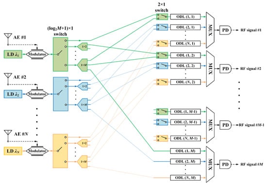
Figure 3.
Illustration of structure equal-precedence.
2.1. Key Parameters Analysis
The aforementioned structures can be compared using several benchmarks, such as system attenuation in the optical domain, the number of switch and splitter elements, and the average number of working switch elements. The optimal structure will be proven by comparing within these parameters.
2.1.1. Number of Switch Elements
The multi-port switch in the reconfigurable structure is constructed by cascading the switch element, which is a 2 × 2 switch, but only one input port is used. The function of the multi-port switch is to reconfigure the optical path and send the optical carrier to the suitable splitter. The number of switch elements in the structure partly represents the hardware and control complexity. The only distinction between the structure DP and EP is the combiner-switch parts before the true-time delay units. But they have the same number of switch elements, which contain N·log2(M) mode-switches and an N·(M − 1) combiner-switch.
2.1.2. Number of Splitter Elements
The splitter is indispensable to the multi-beam receiver and is used to divide the signal into multi-duplication. The multi-stage multi-ports splitter is built like the multi-port optical switch by cascading the basic 1 × 2 splitter elements. The number of splitter elements in the conventional structure is N·(M − 1). In the structure DP and EP, they both have N·(2M − log2M − 2) splitter elements.
2.1.3. System Attenuation
The number of switch elements (1 × 2 switch), splitter elements (1 × 2 splitter), and the delay value of the true-time delay units in a given optical path determine the attenuation. The worst-case attenuation was for the highest path loss. Before the comparison, we assumed that the insert loss caused by the true-time delay line was constant and negligible. We set the insert loss of the switch and splitter elements as X and L, respectively.
In the structure DP, the number of splitter elements in the optical path depends on the current working mode, and the number of switch elements depends on the sequence number of the output ports. When the system works on the m-beam mode, the number of splitter elements in the path is log2(m), the maximum and the minimum number of switch elements is 2·log2[log2(M) + 1] and 2·log2[log2(M/m) + 1], respectively. Thus, the highest loss is L·log2(M) + 2X·log2[log2(M) + 1] when the system is working on the M-mode and the beam signal outputs from ports 1. But the lowest-loss path depends on the relationship between X and L. Although the path within the output has the same attenuation, the path between the output ports has a large difference. The differential attenuation between output ports becomes larger when the system works on the mode which divides the optical power into more parts.
In the structure EP, the lowest-loss path includes log2[log2(M) + 1] + 1 switch elements when the system works in the single-beam mode. The highest-loss path includes log2[log2(M) + 1] + 1 switch elements and log2(M) splitter elements when the system works in the M-beam mode. Thus, the differential attenuation in the structure DP can be expressed as L·log2(M). Compared to the structure DP, the structure EP has less differential attenuation, which is caused only by splitters and is inevitable.
2.1.4. The Average Number of Working Switch Elements
The number of switch elements in the structure only reflects the control complexity in static. The number of working switch elements provides a more visual and dynamic representation of the control complexity—the number of working switch elements changes when the working mode changes. The average number of working switch elements is more comparable and calculated by dividing the sum of the number of switch elements working in each mode by the total number of working modes. As mentioned before, the only difference between the structure DP and EP is the combiner-switch parts. Thus, the total number of the working switch in combiner-switch parts can be compared directly. The number of working switches S in the structure DP can be calculated by the following equation:
meanwhile, the number in the structure EP is 2M − 2.
In summary, the comparison results were plotted in Figure 4 when M = 2, 4, 8, 16, and 32. Clearly, the structure EP has less optical loss than the structure DP in the system attenuation term. Additionally, the structure EP uses fewer switch elements than the structure DP, which means that the structure EP has less power consumption in the control system and is simpler to manipulate. Based on the fact that the structure EP performs better than the structure DP in the system attenuation and the average number of working switch elements, the structure EP will be focused on in the following. The analyses and simulations were performed based on it.
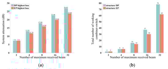
Figure 4.
The comparison of the parameters when beam number N = 2, 4, 8, 16, 32. (a) The comparison of system attenuation with X = 2 dB, L = 3.3 dB; (b) The comparison of total number of working combiner-switch.
2.2. Principle of Operation
The principle of the optimized structure EP is described as follows: The optical switch is controlled to reconfigure the optical path and choose the suitable splitter according to the number of the received beams. After splitting, the optical carriers are sent to the variable true-time delay line units, and the true-time weightings are deployed on the carriers. The multi-wavelength optical carriers from N AEs are combined at the wavelength division multiplexer to form a received beam.
The steps for the configuration of the structure EP are summarized below.
- Initialization. The system works on the M-beam mode by controlling the mode-switch and choosing the splitter with M ports. The M beams are used to search the signal and cover the range with the angle ϕ. Thus, the pointing direction of beam m has φm = (2m – M − 1) · ϕ/(2M − 2). The m-th beam is received from the output m, and the true-time stepping within the m-th port is τm = d·sin(φm)/c. d is the spacing between the adjacent AEs, and c is the speed of the light wave in the vacuum. The true-time delay units within the m-th ports offer the delay vector as τi,m = [0 Δτm … (i − 1)Δτm … (N − 1)Δτm].
- After initializing and signal-searching, we assume that the number of the received signal from different directions is K, and the angles of the received signal are labeled as φ1, φ2, …, φk, …, φK. The system’s working mode is controlled by reconfiguring the optical switch according to the number K. The judgment conditions are described as follows:
- When K = 0, the signals are not received by the system, and the signal searching needs to be performed again by increasing the beam received range. Reconfiguring the optical switch to change the system in order to work on the single-beam mode and the true-time delay line within the first ports periodically offers the delay vector from τi,1 to τi,M. The beam formed in the single-beam mode has the highest power and covers the largest range. As for the newly received signals, we label them φ1, φ2, …, φk, …, φK. If the K is still zero, the signal beyond the system receives the range or is unavailable, and returns to step 1. If the K is changed, the following judges continue to execute;
- When 0 < K < M/2, we choose the suitable working mode by calculating the parameter g with g = 2⎣log2K⎦. We then reconfigure the optical switch to enable the system to work on the g-beam mode. The outputs g to g + K are used to receive the multi-beam. The power of the optical carrier is increased from Pi/M to Pi/g. Pi is the i-th laser power. In the meantime, the delay values are the same as the ports that received the signals at the initial stage., i.e., τi,k = τi,m. The parameter pairs (Pi/g, τi,k) are obtained.
- When K > M/2, the system is kept at the M-beam mode, and all the true-time delay units are set up as the initial stage. The ports that do not receive the signal are used to monitor the original angle. The parameter pairs (Pi/M, τi,k) are obtained from the ports that are used to receive the signal.
- Dynamic detection process: when the system is working, we keep the monitor to the parameter K. If K is changed, we return to step 2. If K is constant, we continue to monitor.
The parameter pair (Pi/M, τi,k) can be used to draw the beam pattern and evaluate the quality of the received beams. The expression of the beam pattern is as follows:
The beam pattern of the multi-beam is the sum of the individual beam pattern, which can be described as:
3. Numerical Simulations
A series of numerical simulations were performed to validate the proposed architecture’s performance in MATLAB. The simulation work developed closely follows the architecture as presented in Figure 3.
The tested phased array antennas (PAA) are settled for a uniformly distributed linear array containing 16 AEs, spaced by half the RF signal wavelength. All the AEs are considered isotropic, and the exciting power is 0 dBm. The frequency of the RF signal is set at 60 GHz. The system support three modes: the single-beam mode, dual-beam mode, and four-beam mode.
Under ideal conditions, the optical switch and the optical splitter are lossless. No extra phase difference will be caused when the signal passes through the optical components. The multi-beam patterns when the receiver works in three modes in such conditions are plotted in Figure 5.
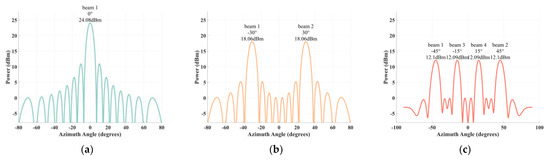
Figure 5.
The multi−beam pattern in ideal condition. (a) single−beam mode; (b) dual−beam mode; (c) four−beam mode.
In Figure 5, when the receiver is working in the single-beam mode, the minimum true-time delay Δτ = 0, the beam direction is 0°, and the main lobe power is 24.08 dBm. When the receiver is working in the dual-beam mode, the minimum true-time delay Δτ = ± 4.17 ps, two beams point toward ±30°, and the main lobe power is 18.06 dBm. When the receiver works in the four-beam mode, the true-time delays Δτ are ±2.16 ps and ±5.89 ps, respectively, the beam directions are ±15° and ±45°, and the four main lobe powers are 12.09 dBm. One conclusion can be drawn by comparing the main lobe power, which is the greater number of the received beam; the main lobe power is lower. Thus, the optical energy can be focused on the beam that is needed to receive by switching the working mode of the system and controlling the signal fed to a suitable splitter. It should be noted here that the four-beam mode has the same performance as the conventional four-beam receiver in ideal conditions.
However, in reality the switch and splitter elements will cause differences in the optical path within and between the output ports. The differences are described as amplitude and phase inconsistency and will influence the quality of the received beams, such as deviating the beam direction, decreasing the main lobe power, and degrading the side lobe suppression ratio. The simulations were performed to evaluate how the introduction of reconfigurable structures affects conventional structures.
The amplitude inconsistency is caused by the additional loss of optical components and the split loss of the splitters. We set those contributions as a random positive value a1 ~ U (0, 121/2), which is a uniform distribution with a variance of 1 dB. The switching speed of the optical switch, the fabrication imperfection of optical components, and the delay accuracy of true-time delay units will cause phase inconsistency. These contributions were set as a random value p1 ~ U (−121/2, 121/2), a uniform distribution with a zero-mean and a variance of 1 ps. The amplitude and phase inconsistency are added on to 16 AEs, and the simulation results are plotted in Figure 6.
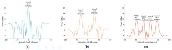
Figure 6.
The multi−beam pattern in amplitude and phase inconsistency with the variances are 1 dB and 1 ps. (a) single−beam mode; (b) dual−beam mode; (c) four−beam mode.
As seen in Figure 6, when the system works in the single-beam mode, the power of the main lobe decreases to 20.59 dBm, and the deflection angle to the pointing direction is 0.4°. When the system works in the dual-beam mode, the powers are lowered to 14.28 and 13.52 dBm, respectively, and the angles of deflection are 0.2° and 0.3°. When the system works in the four-beam mode, the powers are decreased to 9.05, 8.64, 8.41, and 8.31 dBm. The angles of deflection are 0.7°, 0.1°, 0.1°, and 0.2°. Compared to the beam pattern in the ideal condition, the introduction of the reconfigurable structure declines the quality of the multi-beam.
Relieving the influence of the amplitude and phase inconsistency, we set the amplitude error as a random positive value a2~U (0, 31/2), which is a uniform distribution with a variance is 0.5 dB, and the phase error was set as a random value p2~U (−31/2, 31/2), a uniform distribution with zero-mean and a variance of 0.5 ps. The amplitude and phase inconsistency are added on 16 AEs, and the simulation results are plotted in Figure 7.
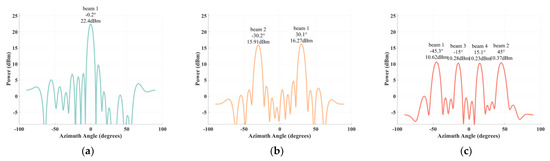
Figure 7.
The multi−beam pattern in amplitude and phase inconsistency with the variances are 0.5 dB and 0.5 ps. (a) single−beam mode; (b) dual−beam mode; (c) four−beam mode.
As shown in Figure 7, the power of the main lobe is 22.40 dBm, and the angle of deflection is 0.2° in the single-beam mode. The powers of the dual main lobe are 16.27 and 15.91 dBm; meanwhile, the deflection angles are 0.1° and 0.2° in the dual-beam mode. As for the four-beam mode, the powers are 10.62, 10.37, 10.28, and 10.23 dBm, and the angles of deflection are 0.3°, 0°, 0.1°, 0°. Compared to the multi-beam patterns in Figure 6, the qualities of the beam are uprising. Thus, when the reconfigurable structure is fabricating and deploying, the amplitude and phase difference between the optical path needs to be balanced and compensated.
4. Discussion
A comparison with related works is given in Table 1. The beamformers proposed in related works are evaluated with a normalized beam pattern to demonstrate the direction of the main lobe and the side lobe depress ratio. However, in this study, the beam pattern is unnormalized. The main lobe’s absolute power is given and used to compare under various working modes. To the best of the authors’ knowledge, this work is the first research to propose a receiver with a variable beam-count. As shown in Figure 5, the main lobe power in a conventional four-beam receiver is fixed at 12.10 dBm. But in the proposed structure, when the system works in a single-beam mode, the main lobe power is 24.08 dBm, and the gain of the array is 11.98 dB. A higher gain means the receiver can capture the signal in a longer range. When the system works in a dual-beam mode, the main lobe power is 18.06 dBm, and the gain of the array is 5.96 dB. It enables the PAA to balance the distance and number of the received beam.

Table 1.
The comparison to related works.
In summary, the reconfigurable structure offers the conventional multi-beam receiver a new degree of freedom: a variable beam-count improves the system’s energy efficiency and adapts the receiver to various communication scenarios.
5. Conclusions
This manuscript presents a novel photonic multi-beam receiver. The working mode can be reconfigured by controlling the optical switch and choosing suitable splitters. According to the communication scenarios, the optical signals are sent to the splitter, which has suitable ports to divide the signal into required numbers. Thus, the optical energy is focused on the desired beam, and the system energy efficiency is improved by controlling the optical switch to reconfigure the optical path. The structures DP and EP have been designed to realize the reconfigurable function. The parameters comparison proves that the structure EP has better performance than the structure DP. Simulation results show the proposed architecture increasing the power of the main lobe when the received beam number is less than the maximum received number. Furthermore, the amplitude and phase inconsistency caused by the reconfigurable structure will decline the quality of the multi-beam. When the value of inconsistency is in a limited range, the balance and compensation of the amplitude and phase should be taken into account when the system is fabricated and deployed.
Future work may include the experimental verifying of the proposed structure and the demonstration of a transmitter architecture with a variable beam-count. We believe that combining these developments will help pave the way for future multi-beam communications.
Author Contributions
Conceptualization, Y.L., J.S. and Q.Q.; methodology, Y.L.; software, Y.L.; validation, Z.F., S.S. and Y.W.; formal analysis, Y.L.; investigation, Y.L.; resources, Y.L.; data curation, Y.L.; writing—original draft preparation, Y.L.; writing—review and editing, Y.L.; visualization, Y.L.; supervision, D.J., Y.C. and X.L.; project administration, Q.Q.; funding acquisition, Q.Q. All authors have read and agreed to the published version of the manuscript.
Funding
This research was funded by the National Natural Science Foundation of China, grant number (No. 62201120 and 61971110), the Natural Science Foundation of Sichuan Province, and the Research Foundation (Y030212059003044).
Institutional Review Board Statement
Not applicable.
Informed Consent Statement
Not applicable.
Data Availability Statement
Further data are available from the corresponding author upon reasonable request.
Conflicts of Interest
The authors declare no conflict of interest.
References
- Saad, W.; Bennis, M.; Chen, M. A Vision of 6G Wireless Systems: Applications, Trends, Technologies, and Open Research Problems. IEEE Netw. 2020, 34, 134–142. [Google Scholar] [CrossRef]
- Alibakhshikenari, M.; Ali, E.M.; Soruri, M.; Dalarsson, M.; Naser-Moghadasi, M.; Virdee, B.S.; Stefanovic, C.; Pietrenko-Dabrowska, A.; Koziel, S.; Szczepanski, S.; et al. A Comprehensive Survey on Antennas On-Chip Based on Metamaterial, Metasurface, and Substrate Integrated Waveguide Principles for Millimeter-Waves and Terahertz Integrated Circuits and Systems. IEEE Access 2022, 10, 3668–3692. [Google Scholar] [CrossRef]
- Hong, W.; Jiang, Z.H.; Yu, C.; Zhou, J.; Chen, P.; Yu, Z.; Zhang, Y.; Chen, J.; He, S. Multibeam Antenna Technologies for 5G Wireless Communications. IEEE Trans. Antennas Propag. 2017, 65, 6231–6249. [Google Scholar] [CrossRef]
- Capmany, J.; Novak, D. Microwave photonics combines two worlds. Nat. Photonics 2007, 1, 319–330. [Google Scholar] [CrossRef]
- Yao, J. Microwave Photonics. J. Light. Technol. 2009, 27, 314–335. [Google Scholar] [CrossRef]
- Song, Q.Q.; Hu, Z.F.; Chen, K.X. Scalable and reconfigurable true time delay line based on an ultra-low-loss silica waveguide. Appl. Opt. 2018, 57, 4434–4439. [Google Scholar] [CrossRef] [PubMed]
- Liu, Y.; Wichman, A.R.; Isaac, B.; Kalkavage, J.; Adles, E.J.; Clark, T.R.; Klamkin, J. Ultra-Low-Loss Silicon Nitride Optical Beamforming Network for Wideband Wireless Applications. IEEE J. Sel. Top. Quantum Electron. 2018, 24, 1–10. [Google Scholar] [CrossRef]
- Wang, G.; Dai, T.; Jiang, J.; Guo, X.; Chen, B.; Wang, Y.; Yu, H.; Jiang, X.; Yang, J. Continuously tunable true-time delay lines based on a one-dimensional grating waveguide for beam steering in phased array antennas. Appl. Opt. 2018, 57, 4998–5003. [Google Scholar] [CrossRef] [PubMed]
- Zhang, X.; Zhao, M.; Jiao, Y.; Cao, Z.; Koonen, A.M.J. Integrated Wavelength-Tuned Optical mm-Wave Beamformer With Doubled Delay Resolution. J. Light. Technol. 2020, 38, 2353–2359. [Google Scholar] [CrossRef]
- Granieri, S.; Jaeger, M.; Siahmakoun, A. Multiple-beam fiber-optic beamformer with binary array of delay lines. J. Light. Technol. 2003, 21, 3262–3272. [Google Scholar] [CrossRef]
- Subbaraman, H.; Chen, M.Y.; Chen, R.T. Photonic Crystal Fiber-Based True-Time-Delay Beamformer for Multiple RF Beam Transmission and Reception of an X-Band Phased-Array Antenna. J. Light. Technol. 2008, 26, 2803–2809. [Google Scholar] [CrossRef]
- Yaron, L.; Rotman, R.; Zach, S.; Tur, M. Photonic Beamformer Receiver with Multiple Beam Capabilities. IEEE Photon. Technol. Lett. 2010, 22, 1723–1725. [Google Scholar] [CrossRef]
- Tsokos, C.; Mylonas, E.; Groumas, P.; Katopodis, V.; Gounaridis, L.; Timens, R.B.; Oldenbeuving, R.M.; Roeloffzen, C.G.H.; Avramopoulos, H.; Kouloumentas, C.; et al. Analysis of a Multibeam Optical Beamforming Network Based on Blass Matrix Architecture. J. Light. Technol. 2018, 36, 3354–3372. [Google Scholar] [CrossRef]
- Ortega, B.; Mora, J.; Chulia, R. Optical Beamformer for 2-D Phased Array Antenna with Subarray Partitioning Capability. IEEE Photon. J. 2016, 8, 1–9. [Google Scholar] [CrossRef]
- Oliveira, R.; Nogueira, R.N.; Drummond, M.V. Multi-Beam Microwave Photonic Beamforming Based on Self-Coherent Detection of a WDM Signal. J. Light. Technol. 2022, 40, 4956–4963. [Google Scholar] [CrossRef]
- Morant, M.; Trinidad, A.; Tangdiongga, E.; Koonen, T.; Llorente, R. Experimental Demonstration of mm-Wave 5G NR Photonic Beamforming Based on ORRs and Multicore Fiber. IEEE Trans. Microw. Theory Tech. 2019, 67, 2928–2935. [Google Scholar] [CrossRef]
- ITU-T G.652. Available online: https://www.itu.int/itu-t/recommendations/rec.aspx?rec=13076 (accessed on 20 December 2023).
Disclaimer/Publisher’s Note: The statements, opinions and data contained in all publications are solely those of the individual author(s) and contributor(s) and not of MDPI and/or the editor(s). MDPI and/or the editor(s) disclaim responsibility for any injury to people or property resulting from any ideas, methods, instructions or products referred to in the content. |
© 2023 by the authors. Licensee MDPI, Basel, Switzerland. This article is an open access article distributed under the terms and conditions of the Creative Commons Attribution (CC BY) license (https://creativecommons.org/licenses/by/4.0/).