Communication

Optical Study on Temperature-Dependent Absorption Edge of γ-InSe-Layered Semiconductor

1
Department of Electrical Engineering, National Taiwan Ocean University, Keelung 202, Taiwan
2
Department of Electrical Engineering, Lunghwa University of Science and Technology, Guishan, Taoyuan 333, Taiwan
3
Department of Electronic Engineering, Lunghwa University of Science and Technology, Guishan, Taoyuan 333, Taiwan
4
Graduate Institute of Applied Science and Technology, National Taiwan University of Science and Technology, Taipei 106, Taiwan
5
Department of Telecommunication Engineering, National Kaohsiung University of Science and Technology, Kaohsiung 811, Taiwan
*
Author to whom correspondence should be addressed.
Appl. Sci. 2024, 14(15), 6676; https://doi.org/10.3390/app14156676
Submission received: 25 May 2024 / Revised: 27 July 2024 / Accepted: 29 July 2024 / Published: 31 July 2024

Abstract

:
We have studied the variations in the temperature-dependent absorption edge of a bulk InSe-layered semiconductor using photoconductivity (PC) measurements. From both the X-ray diffraction (XRD) and Raman experimental results, the structural phase of the as-prepared InSe sample was confirmed to be γ-polytype. Upon heating from 15 K to 300 K, the absorption edge of PC spectra was found to shift significantly toward lower energy, and the absorption edge as a function of temperature was further analyzed by the Varshni’s relationship and Bose–Einstein empirical equation. The Urbach energy as a function of temperature was obtained by fitting the absorption tail below the absorption coefficient of the PC spectrum, and the effective phonon energy can be derived from the temperature-dependent steepness parameter associated with Urbach energy. Our study indicates that the broadening of the absorption edge in the as-synthesized bulk γ-InSe is caused by a combination of electron/exciton–phonon interactions and thermal/structural disorder.

1. Introduction

In recent years, several two-dimensional layered semiconductors, including graphene, transition metal dichalcogenides (TMDCs), and III–VI semiconductors, have been investigated both experimentally and theoretically due to their unique optical, electronic and mechanical properties [1,2,3,4,5]. Among these different layered semiconductors, the indium selenide (InSe) semiconductor consisted of stacked layers of Se-In-In-Se atoms with van der Waals bonding between the quadruplet layers. There are three common polytypes described as β-, ε- and γ-InSe, which differ in the symmetry and structure of the crystal lattice, and display different optical properties [1,4]. Boukhvalov et al. and Shubina et al. have shown that, apart from ε-InSe, which exhibited an indirect bandgap, both β-InSe and γ-InSe have a direct bandgap in the near infrared energy range [1,2]. Accordingly, only β and γ phases of InSe can be developed as an attractive material for versatile optoelectronic devices [3,5,6].
To the best of our knowledge, there are few relevant studies on the temperature dependence of the absorption edge in InSe material [7,8]. Kundakçi et al. and B Gürbulak have investigated the optical properties of InSe single crystal by absorption measurement and observed that an Urbach’s tail appeared below the edge of the absorption spectrum.
However, no information about the actual phase of their samples was provided, and hence only a qualitative comparison can be made. Urbach’s tail or below-band edge optical absorption coefficient (α) can be described by an exponentially varying function with respect to photon energy [9,10]. Cody et al. indicated that the absorption tail below the absorption edge most probably originates from the temperature-independent imperfections of the material and static disorder caused by the impurities, dislocations, or stacking faults [9]. Abay et al. have experimentally and theoretically explained the origin of this tail as exciton–phonon interaction in their material [10]. Therefore, the investigations on Urbach’s tail can provide important information on the localized states extended into the optical gap region, which are related to the structural and thermal disorder, and the electrons/excitons–phonons interactions in the layered semiconductors.
In this work, we reported the temperature dependence of the absorption edge of γ-InSe by analyzing the α derived from photoconductivity (PC) measurements [11,12]. Moddel et al. and Loveland et al. have shown that properly normalized PC data can indeed give an accurate measure of α [11,12]. The energy gap estimated from the PC spectra of γ-InSe as a function of temperatures was analyzed by Varshni’s relationship [13] and the Bose–Einstein empirical equation [14]. Additionally, the effective phonon energy was further obtained based on the temperature dependence of the Urbach energy extracted from PC spectra. The detailed discussion of experimental data can provide useful information for the optoelectronic materials and solar cell devices fabricated by chalcogenides-based layered semiconductors.

2. Experimental Techniques

For the growth of single-crystalline InSe, high-purity 99.999% In and Se compounds were purchased from Sigma Aldrich. The stoichiometry mixture (1:1 of In and Se) was mixed in a quartz ampoule and evacuated to 10−4 Pa. The homogenization of the InSe powders was conducted in a horizontal furnace at 550 °C for two days. The homogenized InSe powders were then transferred into a vertical Bridgman instrument for the growth of the high-quality InSe single crystal. During the Bridgman process, the ampoules containing the InSe mixture were melted in a high-temperature region at 850 °C for a duration of 24 h, and after that, the ampoule was slowly lowered to a low-temperature zone (1 °C at a rate of 0.1 mm/h). The transitions from higher to lower temperatures facilitated the nucleation of large-size InSe single crystals with typical dimensions of 5 cm in length and 1 cm in diameter. The InSe devices were fabricated on a SiO2 (300 nm)/n+-Si substrate. The electrical contacts on the InSe bulk crystals were provided by silver (Ag) paste. The prepared InSe sample was stored in an evacuated container to avoid surface oxidation effects, and the sample was also placed in the vacuum chamber during the optical experiment.
The X-ray diffraction (XRD) analysis of InSe crystals was performed using a Bruker D2 Phaser diffractometer (Bremen, Germany) with Cu-K α radiation under Bragg–Brentano geometry. The Raman scattering experiment was performed using a Micro-Raman spectrometer (HORIBA-iHR550, Kyoto, Japan). In the PC measurement, a monochromatic light source was provided by the Oriel 1000 W (Alameda, CA, USA) halogen light source and the normalized PC signals were collected by a lock-in amplifier and recorded by a computer. The PC measurement was set up to obtain the associated α, which may be difficult to obtain using the conventional techniques, especially in the low-energy region below the band edge [11,12]. It should be noted that in order to obtain a good description of α through PC measurement, some well-defined conditions, as stipulated by Moddel et al., should be satisfied. The conditions of applicability can be facilitated by a proper normalization process [12] of the PC signals. The match had been shown to be quite exact at the near and above band edge regions. Below the band edge in the low energy region, the obtained α derived from PC measurement may be regarded as a lower bound to α. The uncertainty is most likely due to changes in the recombination process of the photoexcited carriers at low energies. Nevertheless, the presently studied energy range of ~1.0 to 1.4 eV (the below-band edge range is ~1.0 to 1.2 eV) falls within a small photon energy range so that a fairly good estimate of α can be provided by the properly normalized PC data.

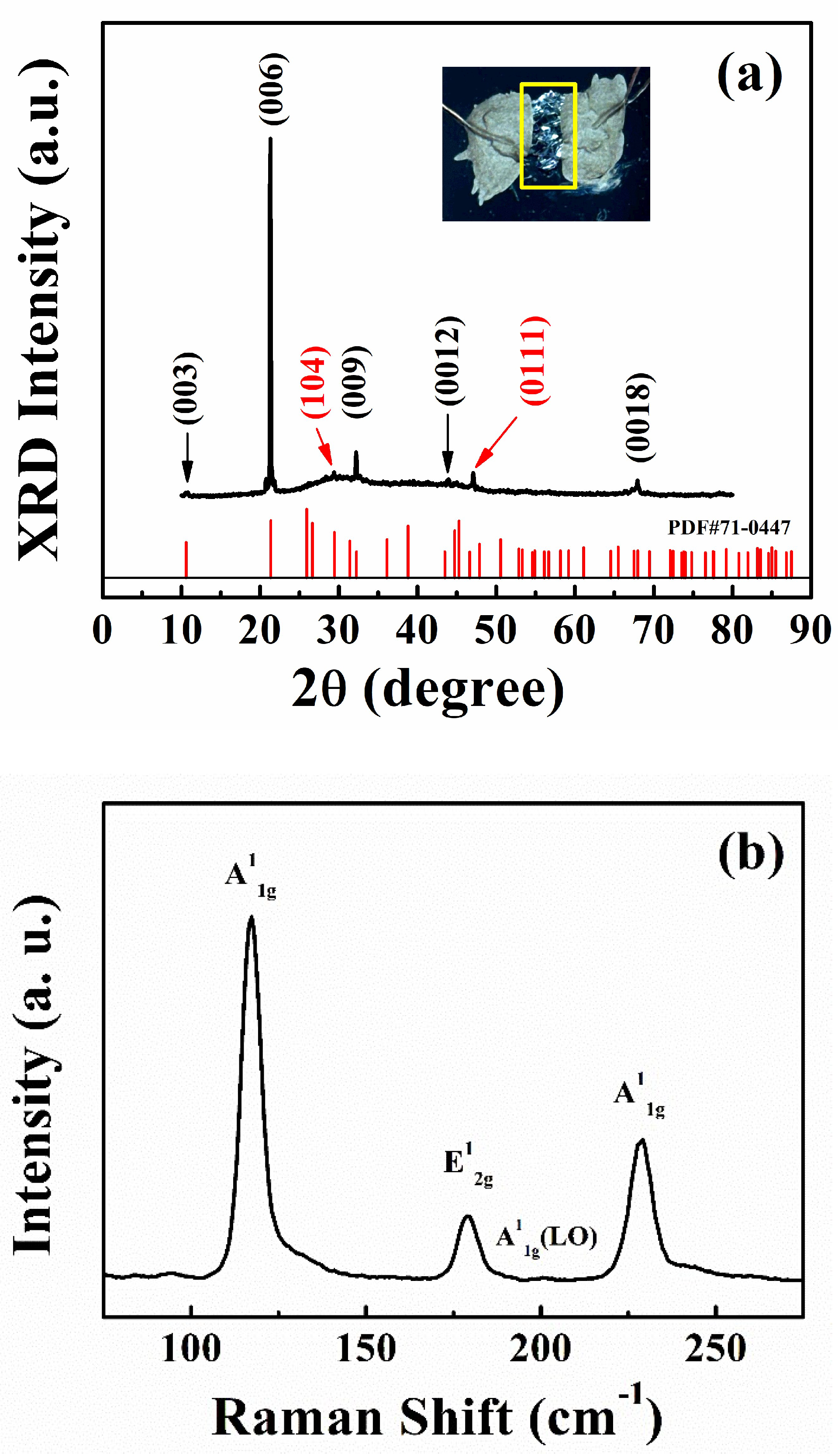
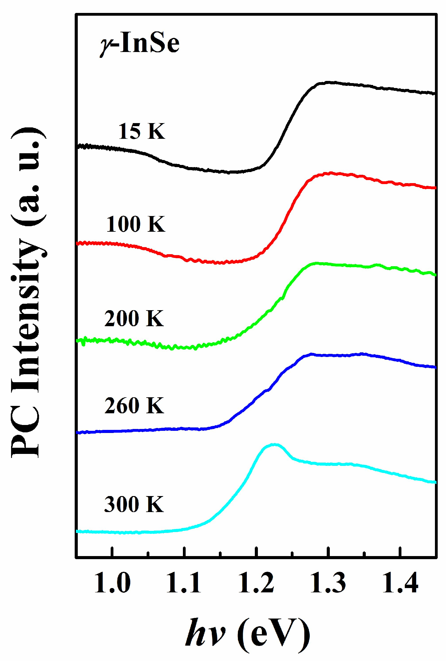
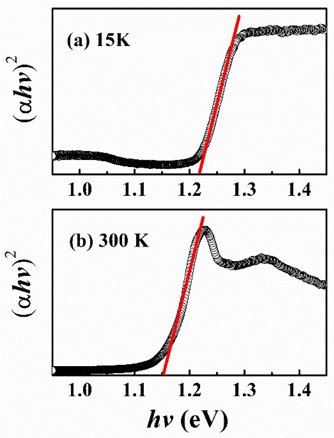
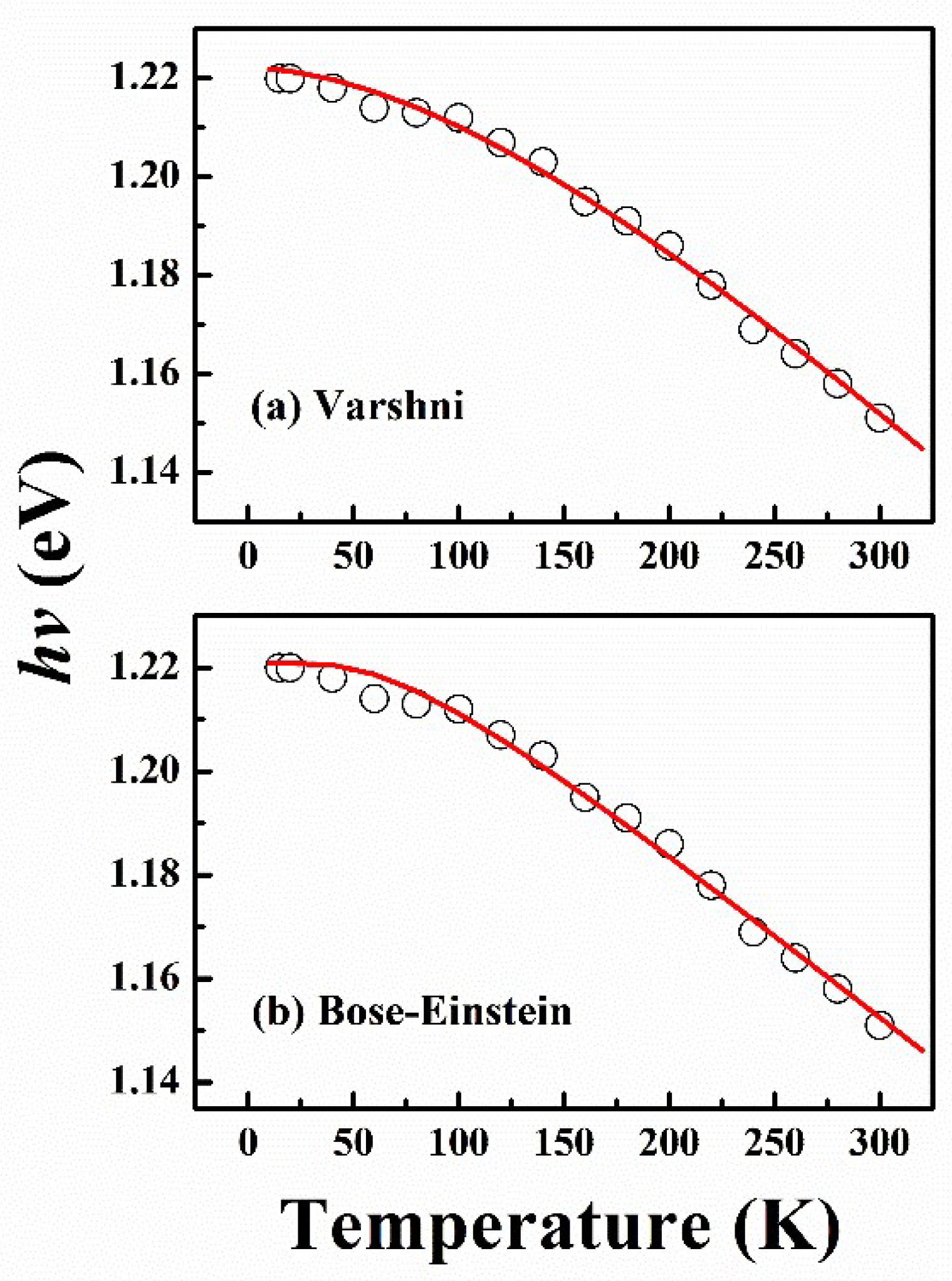
3. Results and Discussion

The XRD pattern and Raman spectrum of the as-grown bulk InSe crystals were measured at room temperature and are depicted in Figure 1a,b, respectively. It is known that the five XRD peaks at about 10.51°, 21.31°, 32.20°, 43.96°, and 67.94°, as labelled and shown in Figure 1a, can be assigned to define the crystal structure of the as-synthesized InSe. Referring to the reported literature [3,4,5,6], Grimaldi et al. [4] Aitzhanov et al. [5] have attributed these peaks to the (0, 0, 2n) planes for the hexagonal β- or ε-polytype, but Wu et al. [3] and Liu et al. [6] have attributed these peaks to the (0, 0, 3n) planes for the γ-polytype. The present uncertainty on the structural phase of the as-grown InSe sample can be resolved by analyzing the two additional diffraction peaks at about 29.41° and 47.05° (marked by the red arrow in Figure 1a).
By comparing the JCPDS (Joint Committee on Powder Diffraction Standards) standard database, the two diffraction peaks at about 29.41° and 47.05° are unable to be defined by the standard data file of PDF 34-1431 for β- or ε-polytype [4,15], but are matched to the standard data file of PDF 71-0447 for γ-polytype and defined as (104) and (0111) plane, respectively [6]. The calculated lattice parameters a = b = 4.32 Å and c = 24.96 Å are in good agreement with the JCPDS #71-0447 (a = b = 4 Å and c = 24.96 Å) [6].
Additionally, Raman spectroscopy can be employed to further clarify the structural phase of the as-synthesized InSe. As shown in Figure 1b, the Raman spectrum exhibits three significant peaks at 117, 178, and 229 cm−1, as well as a weak feature at 200 cm−1. These observed features have been attributed to the A 1 g 1 , E 2 g 1 , A 1 g 2 , and A 1 g 1 ( LO ) modes, respectively [3,4]. It should be noted that the A 1 g 1 ( LO ) mode has been identified as a significant characteristic for the non-centrosymmetric structure of either ε-polytype or γ-polytype [3,4]. The observation of the A 1 g 1 ( LO ) mode signal provides additional evidence to exclude the occurrence of β-polytype. Therefore, by integrating the data from both XRD and Raman analysis, it can be inferred that the structural phase of the as-prepared bulk InSe sample is γ-polytype [6].
Figure 2 shows the normalized PC spectra of γ-InSe in the energy range ~1.0–1.4 eV at selected temperatures of 15, 100, 200, 260, and 300 K.
It is observed that the lower-temperature PC spectra at 15, 100, and 200 K exhibit an initial decrease in PC intensity in the energy range 1.1–1.2 eV. A minimum is observed in the range 1.2–1.25 eV, which increases to a maximum in the range 1.25–1.3 eV, and then finally decreases monotonically with any further increase in photon energy within the investigated energy range. The higher-temperature PC spectra at 260 and 300 K show an almost constant below-band edge PC intensity and increase to a maximum as the photon energy sweeps across the band edge, and then decrease with any further increase in the photon energy. It is noted that the existence of impurity or defect states may play an important role in the PC spectra at low temperature, leading to a larger PC intensity in the vicinity of 1.1 eV. Thermal ionization of the defect states is evident in the observed PC spectra at higher temperature. The temperature dependence of the change in PC intensity can provide information about the fundamental absorption properties of γ-InSe. As stated earlier, correlation of our PC intensity measurements to the relevant absorption coefficient can be found in references [11,12] and will not be elaborated on here. From here on, we use the term absorption coefficient (α) freely in place of normalized PC intensity. It is known that γ-InSe is a direct bandgap material [1,3]. Quereda et al. and Patilhave et al. have used the PC spectroscopy for extraction and estimation of bandgap by using Tauc-relation [16,17], which is given as follows:
α h v 2 = A h v E g
where hv is the photon energy, α is the absorption coefficient, A is a constant, and Eg is the bandgap for the γ-InSe sample. The optical bandgap of the γ-InSe at 15 and 300 K can be extracted by extrapolating the straight line of the plot (αhv)2 versus energy (hv) to the energy axis, as shown in Figure 3a,b. In this way, the bandgap of γ-InSe at 15 and 300 K is estimated to be about 1.220 ± 0.002 and 1.152 ± 0.003 eV, respectively. It is observed that the obtained bandgap value is less than the reported results [1,3], which may be caused by the band tailing effect frequently observed in absorption measurement methods used to estimate bandgap energy [16].
The extracted bandgaps of γ-InSe at different temperatures are displayed as an open circle in Figure 4. The temperature-dependent Eg of γ-InSe are further analyzed by the empirical Varshni’s relationship and Bose–Einstein empirical equation. The Varshni empirical relationship is written as follows [13]:
E g ( T ) = E g ( 0 ) a T 2 T + β
where Eg (0) is the transition energy at 0 K and a and β are constants referred to as Varshni coefficients. The constant a is related to the electron/exciton–phonon interaction and β is approximately equal to the Debye temperature (ΘD) [18].
The Bose–Einstein empirical equation is written as shown in [14]:
E g ( T ) = E g ( 0 ) a B 1 + 2 exp Θ / T 1
where a B represents the strength of the electron/exciton–phonon interaction and Θ corresponds to the average phonon temperature. The theoretical curve, shown as a red solid line in Figure 4a,b, from the empirical Varshni’s relationship and Bose–Einstein empirical equation, respectively, can accurately describe the variations in the temperature-dependent Eg of γ-InSe. The parameters fitted to the empirical Varshni’s relationship and Bose–Einstein empirical equation are obtained and listed in Table 1. The obtained β is about 279 K for Varshni’s equation and the average phonon temperature Θ is about 205 K for the Bose–Einstein relation. It is known that the Θ is closely related to the Debye temperature (ΘD) by the relation Θ   3 4 Θ D [18]. Hence, the estimated Debye temperature in this work is about 273 K, which is in close agreement with the fitted parameter β . The good agreement indicates consistency of our fitted parameters using both Varshni’s and Bose–Einstein’s empirical equation.
Additionally, all PC spectra of the bulk γ-InSe sample at different temperatures shown in Figure 2 displayed a significant absorption tail below the absorption coefficient, which is known as Urbach’s tail. Numerous theoretical and experimental studies about the origin of this tail have been presented. Zhu et al. have indicated that the width of the absorption tail is related to localized states in the optical gap of material, which are associated with structural and thermal disorder or a low-quality crystalline structure [19]. Abay et al. have attributed the absorption tail to the electron–exciton interaction with phonons in the layered semiconductors [10]. To understand the effects of defect states or electronic/exciton–phonon interaction in the bulk γ-InSe sample, the absorption coefficient near the absorption edge is further investigated by the Urbach’s tail model as an exponential relation form, as shown in [19,20]:
α α 0 exp ( h v / E U )
where α 0 is a constant, and E U is the Urbach energy that has the dimensions of energy to describe the distribution of tail states extending into the forbidden gap. As shown in Figure 5, the Urbach’s tail in the absorption edge for the γ-InSe at 15 K and 300 K can be well described by the red solid line calculated using Equation (4). According to the fits, the Urbach energy E U as a function of temperature is extracted and plotted in Figure 6a.
Furthermore, the Urbach energy can be expressed by an inverse logarithmic slope relation E U = k B T / σ ( T ) , where k B is the Boltzmann constant and the σ ( T ) is called the steepness parameter [19,20]. Figure 6b shows the temperature-dependent steepness parameter, which is derived from the Urbach energy as plotted in Figure 6a. The relationship between the steepness parameter σ , temperature, and phonon energy is discussed in detail by [19,20] and is written as follows:
σ ( T ) = σ 0 2 k B T h v p tanh ( h v p 2 k B T )
where σ 0 is a temperature-independent but material-dependent constant. The h v p is attributed to the effective phonon energy in the single-oscillator model describing certain information about the interaction of electrons and/or excitons with phonons in semiconductors. The red solid line displayed in Figure 6b represents the best fit to the derived σ ( T ) data and the estimated value of h v p is about 52 meV, which is the effective average energy of phonons contributing to the Urbach tails. It has to be noted that the obtained value of h v p is almost double that of the actual phonon energy of about 28 meV, which is calculated using the observed highest optical mode ( A 1 g 2 at 229 cm−1) in the Raman spectrum shown in Figure 1b. The larger h v p indicates that in addition to the electron/exciton–phonon interaction, extra effects also contribute significantly to the effective phonon energy. Similar results have been investigated in previous reports [10,20,21]. Abay et al. have attributed the origin in the higher value of h v p observed in mixed chalcogenides to the structural disorders caused by cation–cation disorder, cation vacancies, and interstitials [10]. Rincón et al. and Hwang et al. indicated that larger h v p values could result from enhanced electronic distortion originating from the ordered defects and structural disorder caused by compositional deviation from the ideal stoichiometry [20,21].
The contributions from both thermal-induced and structural disorders for non-ideal single crystals should be incorporated into the consideration of the increased E U [21,22]. The temperature dependence of E U can be described by an Einstein oscillator model, which take into account contributions of dynamic thermal and static structural disorders. The relation is expressed as [10,23]:
E U = A ( 1 e Θ E T - 1 ) + B
where A and B are adjustable parameters related to the modification of thermal phonon distribution and structural disorders, respectively, and Θ E is the Einstein temperature [18]. Pejova et al. further indicated that the first term in Equation (6) represents the contribution of electron/exciton–phonon interaction, and the second term is due to the mean-square deviation of atomic positions from a perfectly ordered lattice, caused by the structural disorder [23]. It is noted that structural disorder is independent of temperature, and the structural disorders would form due to the existence of multiple structural defects associated with the two-dimensional dislocation or complex stacking arrangements of the constituent elements in the layered lattice for the layered materials [24]. As shown in Figure 6a, the red solid line represented by Equation (6) can accurately describe the temperature dependence of E U . The fitted values of A, B, and Θ E are 17.7 meV, 18.6 meV and 198 ± 10 K, respectively. By computing with the fitted value of A, the contribution of the thermally induced disorder at low temperature of 15 K shows a negligibly small thermal disorder. The room temperature thermal disorder is evaluated to be about 18.9 meV and is slightly larger than that of the structural disorder. Our analysis indicates that the contribution of E U in the InSe-layered materials is dominated by the structural disorder at low temperature and thermal disorder becomes significant as the temperature increases.

4. Conclusions

The temperature-dependent energy gap Eg of γ-InSe extracted from the PC spectrum has been well fitted with the Varshni’s relationship and Bose–Einstein models. From the temperature dependence of the steepness parameter related with Urbach energy in the PC spectra, the associated effective phonon energy has been evaluated to be about 52 meV. The investigations on the obtained value of effective phonon energy indicate that not only electron/exciton–phonon interaction but also thermal and structural disorders lead to the broadening of Urbach’ tail in the γ-InSe-layered semiconductor.

Author Contributions

Writing—original draft preparation, W.-T.W.; supervision, K.-K.T.; investigation, S.-W.T.; formal analysis, S.-Y.H.; writing—review and editing, Y.-C.L.; resources, R.-S.C.; validation, C.-T.W. All authors have read and agreed to the published version of the manuscript.

Funding

National Science Council Project No. MOST 109-2637-E-236-001.

Data Availability Statement

The original contributions presented in the study are included in the article, further inquiries can be directed to the corresponding author.

Conflicts of Interest

The authors declare no conflict of interest.

References

  1. Boukhvalov, D.W.; Gürbulak, B.; Duman, S.; Wang, L.; Politano, A.; Caputi, L.S.; Chiarello, G.; Cupolillo, A. The advent of indium selenide: Synthesis, electronic properties, ambient stability and applications. Nanomaterials 2017, 7, 11–372. [Google Scholar] [CrossRef]
  2. Shubina, T.V.; Desrat, W.; Moret, M.; Tiberj, A.; Briot, O.; Davydov, V.Y.; Platonov, A.V.; Semina, M.A.; Gil, B. InSe as a case between 3D and 2D layered crystals for excitons. Nat. Commun. 2019, 10, 3479. [Google Scholar] [CrossRef] [PubMed]
  3. Wu, M.; Xie, Q.; Wu, Y.; Zheng, J.; Wang, W.; He, L.; Wu, X.; Lv, B. Crystal structure and optical performance in bulk γ–InSe single crystals. AIP Adv. 2019, 9, 025013. [Google Scholar] [CrossRef]
  4. Grimaldi, I.; Gerace, T.; Pipita, M.M.; Perrotta, I.D.; Ciuchi, F.; Berger, H.; Papagno, M.; Castriota, M.; Pacilé, D. Structural investigation of InSe layered semiconductors. Solid State Commun. 2020, 311, 133855. [Google Scholar] [CrossRef]
  5. Aitzhanov, M.; Guseinov, N.; Nemkayeva, R.; Tolepov, Z.; Prikhodko, O.; Mukhametkarimov, Y. Inse crystals obtained by stoichiometric fusion for optoelectronic device application. J. Nano-Electron. Phys. 2021, 13, 05037. [Google Scholar] [CrossRef]
  6. Liu, W.; Yang, X.; Wang, Z.; Li, Y.; Li, J.; Feng, Q.; Xie, X.; Xin, W.; Xu, H.; Liu, Y. Self-powered and broadband opto-sensor with bionic visual adaptation function based on multilayer γ-InSe flakes. Light Sci. Appl. 2023, 12, 180. [Google Scholar] [CrossRef] [PubMed]
  7. Kundakçi, M.; Gürbulak, B.; Doğan, S.; Ateş, A.; Yildirim, M. Urbach tail and electric field influence on optical properties of InSe and InSe:Er single crystals. Appl. Phys. A 2008, 90, 479. [Google Scholar] [CrossRef]
  8. Gürbulak, B. Urbach Tail and Optical investigations of Gd doped and undoped InSe single crystals. Phys. Scr. 2004, 70, 197. [Google Scholar] [CrossRef]
  9. Cody, G.D.; Tiedje, T.; Abeles, B.; Brooks, B.; Goldstein, Y. Disorder and the optical-absorption edge of hydrogenated amorphous silicon. Phys. Rev. Lett. 1981, 47, 1480. [Google Scholar] [CrossRef]
  10. Abay, B.; Güder, H.S.; Efeoğlu, H.; Yoğurtçu, Y.K. Temperature dependence of the optical energy gap and Urbach Martienssen’s tail in the absorption spectra of the layered semiconductor Tl2GaInSe44. J. Phys. Chem. Solids 2001, 62, 747. [Google Scholar] [CrossRef]
  11. Moddel, G.; Anderson, D.A.; Paul, W. Derivation of the low-energy optical-absorption spectra of a-Si:H from photoconductivity. Phys. Rev. B 1980, 22, 1918. [Google Scholar] [CrossRef]
  12. Loveland, R.J.; Spear, W.E.; Al-Sharbaty, A. Photoconductivity and absorption in amorphous Si. J. Non-Crystal. Solids 1973, 13, 55. [Google Scholar] [CrossRef]
  13. Varshni, Y.P. Temperature dependence of the energy gap in semiconductors. Physica 1967, 34, 149. [Google Scholar] [CrossRef]
  14. Lantenschlager, P.; Garriga, M.; Logothetidis, S.; Cardona, M. Interband critical points of GaAs and their temperature dependence. Phys. Rev. B 1987, 35, 9174. [Google Scholar] [CrossRef] [PubMed]
  15. Hao, Q.; Yi, H.; Su, H.; Wei, B.; Wang, Z.; Lao, Z.; Chai, Y.; Wang, Z.; Jin, C.; Dai, J.; et al. Phase identification and strong second harmonic generation in pure ε-InSe and its alloys. Nano Lett. 2019, 19, 2634. [Google Scholar] [CrossRef] [PubMed]
  16. Quereda, J.; Ghiasi, S.T.; van Zwol, F.A.; van der Wal, C.H.; van Wees, B.J. Observation of bright and dark exciton transitions in monolayer MoSe2 by photocurrent spectroscopy. 2D Mater. 2018, 5, 015004. [Google Scholar] [CrossRef]
  17. Patil, P.D.; Wasala, M.; Ghosh, S.; Lei, S.; Talapatra, S. Broadband photocurrent spectroscopy and temperature dependence of band gap of few-layer indium selenide (InSe). Emerg. Mater. 2021, 4, 1029. [Google Scholar] [CrossRef]
  18. Trapalis, A.; Farrer, I.; Kennedy, K.; Kean, A.; Sharman, J.; Heffernan, J. Temperature dependence of the band gap of zinc nitride observed in photoluminescence measurements. Appl. Phys. Lett. 2017, 111, 122105. [Google Scholar] [CrossRef]
  19. Zhu, J.; Xia, Y.; Li, G.; Zhou, S.; Wimmer, S.; Springholz, G.; Pashkin, A.; Helm, M.; Schneider, H. Absorption edge, urbach tail, and electron-phonon interactions in topological insulator Bi2Se3 and band insulator (Bi0.89In0.11)2Se3. Appl. Phys. Lett. 2019, 114, 162105. [Google Scholar] [CrossRef]
  20. Rincón, C.; Wasim, S.M.; Marín, G.; Márquez, R.; Nieves, L.; Sánchez Pérez, G.; Medina, E. Temperature dependence of the optical energy gap and Urbach’s energy of CuIn5Se8. J. Appl. Phys. 2001, 90, 4423. [Google Scholar] [CrossRef]
  21. Hwang, Y.; Choi, J.; Ha, Y.; Cho, S.; Park, H. Electronic and optical properties of layered chalcogenide FeIn2Se4. Curr. Appl. Phys. 2020, 20, 212. [Google Scholar] [CrossRef]
  22. Wasim, S.M.; Marín, G.; Marquez, R.; Rincón, C. On the effect of structural disorders on the Urbach’s tails of ternary chalcopyrite semiconductors and related ordered defect compounds. J. Appl. Phys. 2020, 127, 035703. [Google Scholar] [CrossRef]
  23. Pejova, B.; Abay, B.; Bineva, I. Temperature dependence of the band-gap energy and sub-band-gap absorption tails in strongly quantized ZnSe nanocrystals deposited as thin films. J. Phys. Chem. 2010, C114, 15280. [Google Scholar] [CrossRef]
  24. Rudenko, A.N.; Katsnelson, M.I.; Gornostyrev, Y.N. Dislocation structure and mobility in the layered semiconductor InSe: A first-principles study. 2D Mater. 2021, 8, 045028. [Google Scholar] [CrossRef]
Figure 1. (a) XRD patterns (b) Raman spectra of the grown InSe crystals.
Applsci 14 06676 g001
Figure 2. The normalized PC spectra of InSe at selected temperatures between 15 and 300 K.
Applsci 14 06676 g002
Figure 3. Bandgap extraction using extrapolation at (a) 15 K and (b) 300 K.
Applsci 14 06676 g003
Figure 4. The experimental values of the temperature dependence of E g ( T ) for InSe. Solid lines represent the best fit to (a) Varshni and (b) the Bose–Einstein equation.
Applsci 14 06676 g004
Figure 5. Urbach’s absorption tail in the PC spectrum at 15 and 300 K for InSe. Solid lines represent the best fit to Equation (4).
Applsci 14 06676 g005
Figure 6. (a) Urbach energy ( E U ) and (b) steepness parameter ( σ ) as a function of the temperature for InSe. The solid line represents the best fit to Equations (5) and (6) for the temperature-dependent Urbach energy and steepness parameter, respectively.
Applsci 14 06676 g006
Table 1. Values of the parameters obtained from a fit to the Varshni and Bose–Einstein equation.
VarshniEg(0) (eV) a (eV/K)β (K)
1.221 ± 0.0024.6 × 10−4279 ± 10
Bose–EinsteinEg(0) (eV) a B (meV) Θ (K)
1.220 ± 0.00220.6 ± 0.5205 ± 10
Disclaimer/Publisher’s Note: The statements, opinions and data contained in all publications are solely those of the individual author(s) and contributor(s) and not of MDPI and/or the editor(s). MDPI and/or the editor(s) disclaim responsibility for any injury to people or property resulting from any ideas, methods, instructions or products referred to in the content.

