Article

Systematic Analysis of Spacer and Gate Length Scaling on Memory Characteristics in 3D NAND Flash Memory

Department of Semiconductor Engineering, Seoul National University of Science and Technology, Gongneung-ro 232, Nowon-gu, Seoul 01811, Republic of Korea
*
Author to whom correspondence should be addressed.
Appl. Sci. 2024, 14(15), 6689; https://doi.org/10.3390/app14156689
Submission received: 7 July 2024 / Revised: 28 July 2024 / Accepted: 29 July 2024 / Published: 31 July 2024

Abstract

:
This study investigates the impact of oxide/nitride (ON) pitch scaling on the memory performance of 3D NAND flash memory. We aim to enhance 3D NAND flash memory by systematically reducing the spacer length (Ls) and gate length (Lg) to achieve improved memory characteristics. Using TCAD simulations, we evaluate the effects of Ls and Lg scaling on the program speed, erase speed, and Z-interference. Furthermore, we examine the influence of concave and convex channel structures in the context of Ls and Lg scaling. By analyzing the distributions of electron and hole-trapped charges, we provide insights into optimizing the trade-offs between the memory window and retention characteristics. This research offers valuable guidelines for improving the reliability and performance of 3D NAND flash memory through a systematic analysis of spacer and gate length scaling.

1. Introduction

Balancing data access speed and storage density is a critical challenge in modern data storage technologies. Fast data access and high-density storage are increasingly essential requirements across various applications. While conventional high-bandwidth memory (HBM) solutions offer effective performance, they are prohibitively expensive and limited in capacity, presenting significant barriers to widespread adoption in large-scale deployments [1]. In contrast, NAND flash memory provides a compelling alternative due to its low cost and high storage capacity. By utilizing NAND flash memory instead of HBM, it is possible to achieve the necessary memory capacity without incurring prohibitive costs [2,3]. Therefore, enhancing the bit density in NAND flash memory is crucial for advancing modern storage systems. To meet these demands, 3D NAND flash memory requires technological advancements to reduce device size and lower costs. However, the non-ideal threshold voltage (Vth) shift phenomenon, which occurs during the scaling-down process of existing memory arrays, negatively impacts the performance of flash memory [4,5,6].
Recently, numerous studies have focused on changes in memory characteristics due to a decrease in oxide/nitride (ON) mold pitch to address process and device issues arising from an increase in the number of stacked layers [7,8,9]. As the ON pitch decreases, the distance between each word line (WL) diminishes, accelerating Z-interference degradation and reducing the cell’s distribution margin [10]. Additionally, as the program speed decreases and program/erase (PE) window characteristics deteriorate, securing reliable characteristics becomes challenging due to the reduced cell’s distribution margin. While there are many studies on this phenomenon of program speed reduction, most analyze characteristics by reducing oxide and nitride at the same proportion within the ON pitch [9].
Consequently, there is a lack of a clear analysis on the intrinsic program, erase and read characteristics, and overall memory characteristics when individually scaling the spacer length (Ls) and gate length (Lg) corresponding to the oxide and nitride thicknesses. In this study, we conducted a comprehensive analysis of the factors affecting the memory window, Z-interference, and data retention while systematically reducing Ls and Lg at a given ON mold pitch. Furthermore, to mitigate the program speed slowdown and Z-interference degradation that inevitably occur due to ON pitch reduction, we propose the introduction of optimal curvature poly-Si channels during Ls and Lg scaling.
Through this study, we aim to provide important guidelines for improving the bit density in 3D NAND flash memory by analyzing the causes of changes in memory characteristics during ON pitch scaling and suggesting methods to enhance memory performance during the development of 3D NAND devices.

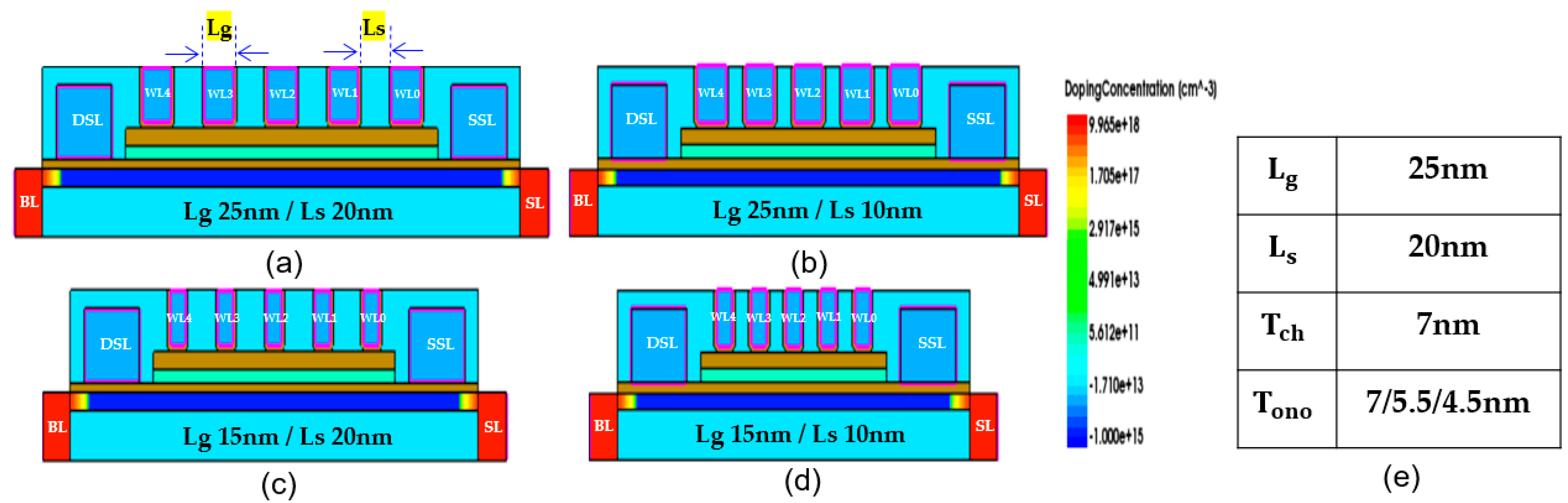
2. Simulation Set-Up

To analyze device operation characteristics according to ON pitch scaling, we implemented a simulation structure, as shown in Figure 1. Physical parameters were referenced from previous 3D NAND research results [11]. The blocking oxide, charge trap nitride, and tunneling oxide layers are 7 nm, 5.5 nm, and 4.5 nm, respectively. The gate length (Lg) of the reference structure shown in Figure 1a is 25 nm, the spacer length (Ls) is 20 nm, and the channel thickness is set to 7 nm. To simulate the scaling effects of Lg and Ls, four structures with different ON pitches were implemented through TCAD simulation. All other parameters were kept fixed while either Ls was reduced to 10 nm, as shown in Figure 1b, or Lg was reduced to 15 nm, as shown in Figure 1c. Additionally, to confirm the interaction when both Lg and Ls are reduced, a structure in which both parameters are reduced, as shown in Figure 1d, was also compared.
The 2D NAND structure set in this way was implemented as a 3D NAND structure through the cylindrical function. The design allows for the use of either a Drain Select Line (DSL) or Source Select Line (SSL), and the 3D NAND structure is composed of a total of five cells, including the Select Line connected to the Bit Line (BL) and Source Line (SL). The simulation was conducted with these configurations. Tungsten was used as the gate material, and the gate edge was analyzed based on a rounded shape of 2 nm each, considering the actual process implementation of the device. The source and drain were doped with phosphorus at a concentration of 1 × 1019 cm−3, and the polysilicon channel was doped with boron at a concentration of 1 × 1015 cm−3.
The operating conditions for the program, erase, and read operations are listed in Table 1. During the program operation, 17 V was applied to the selected cell, and 5 V was applied as the pass voltage. The erase voltage was achieved by applying 0 V to all gates and 20 V to BL and SL to generate a Gate-Induced Drain Leakage (GIDL) current. During the read operation, 3.3 V was applied to SSL and DSL, 0.5 V to BL, and 5.5 V to all unselected cells. A voltage ranging from −5 V to 5 V was applied to the selected WL to check the Id-Vg curve, and the gate voltage at which 50 nA flows was defined as Vth. The Z-interference was defined as the shift in the victim cell’s Vth after programming the attack cell. This measurement was performed by keeping the victim cell Vth constant after erase, considering that the initial Vth of each ON pitch device varies greatly, and then changing the programmed Vth of the attack cell equally.

3. Analysis of Program and Erase Window

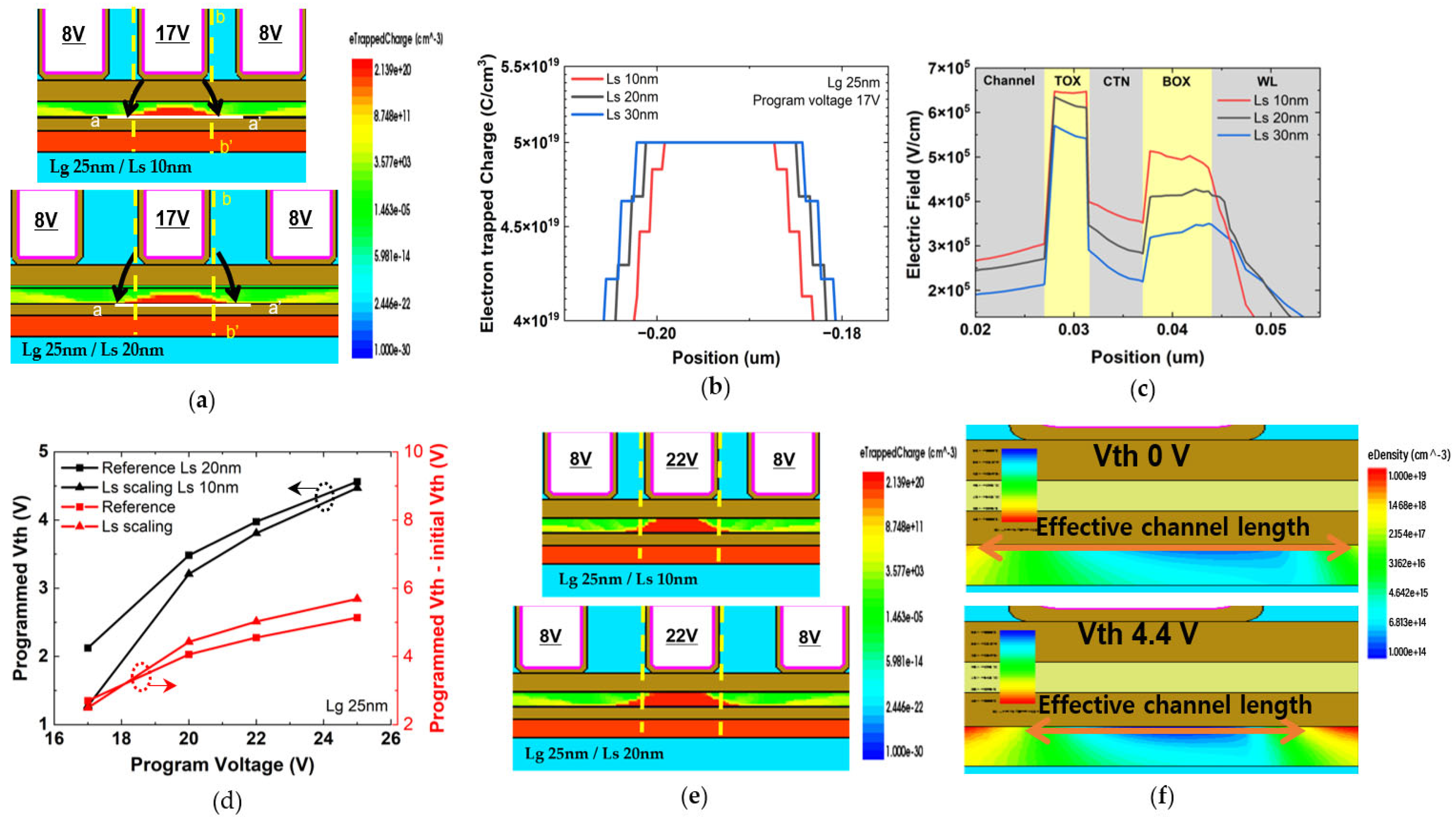
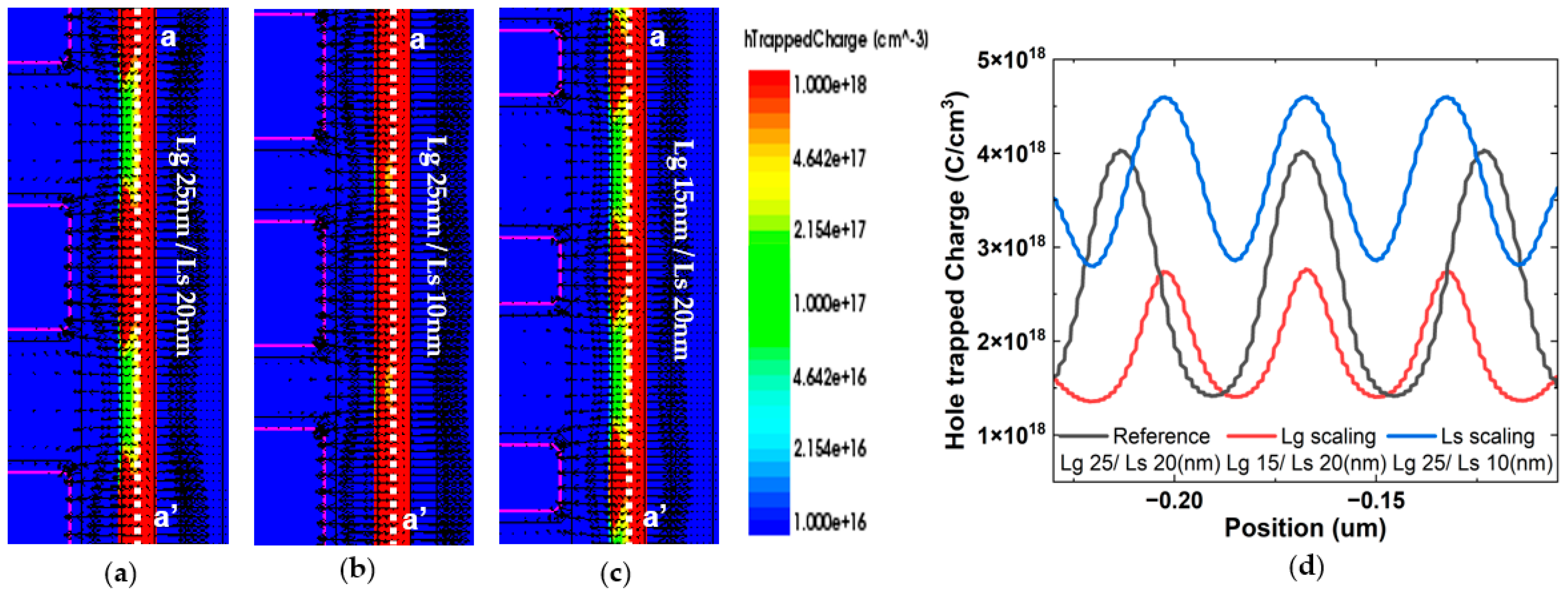
3.1. Program Window Effect

Figure 2a shows the value of the programmed Vth read after applying the same program voltage to each structure. Additionally, the initial Vth value, measured by a simple read operation without additional program or erase operations, is simultaneously represented. Even though the overall ON pitch length is the same, the reduction rate of Vth varies significantly in each structure of Lg scaling, Ls scaling, and both Lg/Ls scaling. To separate the Vth reduction effect caused by the short channel effect (SCE) due to a reduction in the device size and the Vth variability effect caused by the distribution of trapped electrons in the charge trap layer (CTL) after the program operation, two Vth values were compared simultaneously. As shown in Figure 2a, the Vth reduction effect after programming was more noticeable in all three scaling cases compared to the Vth reduction effect due to the initial read operation. This is because the conduction change in the poly-Si channel that occurs as electrons are trapped within the CTL is added along with the Vth reduction phenomenon due to the SCE that occurs as the devices become smaller.
The results indicate that the programmed Vth decrease is the largest during Lg scaling in both the initial read operation and the Vth change amount after the program operation. Therefore, to compare only the amount of change in Vth caused by the charge stored in the cell after programming, a graph of the initial Vth subtracted from the programmed Vth is shown in Figure 2b. This clearly confirms that the Vth reduction due to program operation deteriorates by more than four times during Lg scaling compared to Ls scaling.
To analyze the cause of Vth reduction after programming, Figure 3a–d show the e-trapped charge distribution within the CTL when the selected WL of the proposed 3D NAND device was programmed to 17 V. As the dimensions of each device change, the electric field applied to the gate dielectric and poly-Si channel is formed differently, resulting in varying amounts of charge being trapped in each structure. Obviously, the amount of charge trapped in the entire CTL tends to increase as the gate area increases. Therefore, to check in more detail the concentration of electrons trapped in the CTL compared to the gate area, the e-trapped charge of the reference and Lg scaling structures of the CTL are shown in Figure 3e. A quantitative comparison was made by cutting the a-a’ area. The results indicate that the length of the selected WL decreased by 40% from 25 nm to 15 nm during Lg scaling compared to the reference, while the length of the region where the e-trapped charge in the CTL was more than 5 × 10¹⁹ C/cm−3 decreased by 54%. This suggests that the decrease in the concentration of e-trapped charges in the gate edge area during Lg scaling is the main cause of the decrease in the programmed Vth. The effect of reducing the electron concentration in the gate edge area when Lg is reduced is explained by the reduction in capacitive coupling on the WL to the poly-Si channel substrate [12]. When a program voltage is applied to the selected WL, there is no metal electrode in the space area, so a direct voltage is applied to the lower area of the gate. Still, other voltages due to the fringing field are distributed and applied to the space area. When the area of the gate is reduced compared to the substrate, the effective program voltage decreases in the space area due to a decrease in the fringing field, causing a decrease in the electron concentration, especially in the gate edge area. Therefore, to maximize the effect of reducing the gate edge electron concentration, it is important to make the gate edge shape as right-angled as possible rather than rounding it, as shown in Figure 4a,b. Figure 4c compares quantitative e-trapped charge values by cutting the a-a’ of Figure 4a,b. Even though the ON pitch is the same, there is a clear difference in the electron concentration in the edge area due to the gate edge rounding effect at the 2 nm level. Thus, as the ON mold pitch decreases, it becomes necessary to closely examine the structural shape of the edge area in contact with the oxide and precisely control the related processes. For example, modifying the material composition of the silicon nitride layer to control the etching rate can be a key solution for creating angled corners [11]. During the CVD deposition process of the nitride material in the ON (oxide/nitride) mold formation, adjusting the flow rate of SiH4 can vary the composition ratio of the nitride material adjacent to the oxide. This adjustment increases the etching rate of the adjacent nitride material during wet etching, thus facilitating the creation of angled corners. These methods are practical solutions for forming the desired corner shapes while reducing process complexity.
Meanwhile, as confirmed in Figure 2a,b, it can be seen that the threshold voltage decreases even in the Ls scaling structure, although to a lesser extent compared to Lg scaling. To analyze the cause of program speed reduction in the Ls scaling structure, the e-trapped charge according to the Ls change was compared to when Lg was fixed, as shown in Figure 5a,b. Figure 5b is the result of a quantitative comparison of the electron-trapped charge by cutting a-a’ of the CTL in Figure 5a. Similar to the decrease in Lg, it shows that as Ls decreases, the e-trapped charge distribution becomes narrower. Figure 5c shows the electric field value confirmed by cutting the b-b’ area in Figure 5a. As the Ls value decreases, the influence of the pass voltage applied to the adjacent WL on the electric field of the selected WL increases. Therefore, the program voltage on the selected WL becomes more concentrated in the cell area of the selected WL, which forms a narrow distribution of e-trapped charges in the charge trap layer of the selected WL. On the other hand, when Ls is larger, the program voltage applied to the selected WL is distributed toward the surrounding WL, showing a relatively wide distribution. Thus, it can be inferred that when Ls decreases, the programmed Vth is read as smaller due to the relatively narrow distribution of electrons.
Additionally, we examined how the program would change if the program voltage applied to the selected WL was as high as 22 V. Figure 5d shows the change in the programmed Vth with an increased program voltage applied to the selected WL during Ls scaling. The results show that as the program voltage increases, the reduction effect of the programmed Vth due to Ls reduction decreases. Figure 5e confirms the e-trapped charge distribution in the CTL when programmed at 22 V. As seen in Figure 5a, with 17 V programming, the electron concentration distribution is still narrow when scaling Ls compared to the reference. This difference in the distribution of electron concentration in the space region will have a greater impact on the change in channel resistance during the read operation, so the difference in the programmed Vth is expected to be maintained or the gap may widen further. However, in Figure 5d, the difference in the programmed Vth decreases at higher program voltages. The reversal of this trend at higher voltages can be interpreted as changes in the fringing field of the read voltage applied to the selected WL depending on the programmed Vth value. Figure 5f shows the electron density of the channel when the read voltage corresponding to Vth is applied to each selected WL, with a high programmed Vth at 4.4 V and a low one at 0 V after the program operation. The Vth is defined as the read voltage when 50 nA flows in the poly-Si channel. As a result, when the Vth is high, a high read voltage is applied to the selected WL, causing a large fringing field applied to the bottom of the poly-Si channel, resulting in a small effective gate length. Conversely, when the Vth is low, 0 V is applied to the selected WL, leading to a small fringing field and a large effective gate length. This means that in the high programmed Vth region, the influence of the electron concentration spread from the gate edge to the space region on the read operation is significantly reduced. Therefore, in Figure 5d, it can be interpreted that when Ls is reduced, the higher the program voltage of the selected WL, the less sensitive the reduction effect of the programmed Vth becomes, and the smaller the Vth gap with the reference device. Additionally, the red graph in Figure 5d represents the programmed Vth minus the effect of the initial read operation observed in Figure 2a. Looking at the results, it can be seen that in areas where the program voltage is high, the Vth difference in the Ls scaling case forms a higher value. This reversal phenomenon can be interpreted as a result of the increased concentration of e-trapped charges becoming more dense in the lower part of the selected WL when scaling Ls compared to the reference.

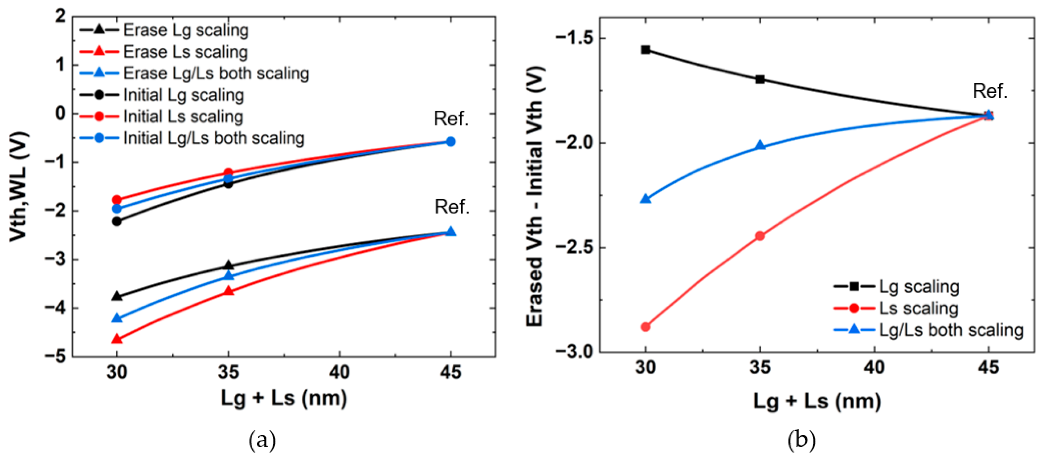
3.2. Erase Window Effect

Figure 6a shows the initial Vth and erased Vth values for each proposed ON pitch structure. As in the program analysis, the erased Vth and initial Vth values are shown in Figure 6b to check only the Vth change pattern due to the hole-trapped charge stored in the CTL, excluding the Vth reduction phenomenon due to the read operation caused by the SCE. The results indicate that in Ls scaling, the Vth decreases and the erase window improves, while in Lg scaling, the Vth increases and the erase window deteriorates. The decrease in Vth during Ls scaling is interpreted as an increase in the fringing field effect caused by adjacent WLs [13].
To clarify this, the hole-trapped charge in the CTL after the erase operation was examined, as shown in Figure 7a–c. The results confirm that during Ls scaling, compared to the reference, a high hole concentration occurs not only in the selected WL but also in the space area due to the strengthening of the fringing field with the adjacent WL. A quantitative comparison of the hole concentration trapped in the CTL for each structure was made by cutting the a-a’ direction in Figure 7a–c. Figure 7d shows that during Ls scaling, compared to the reference, a very high hole concentration is confirmed in the selected WL and space area. However, during Lg scaling, a hole concentration at only 50% of the reference is quantitatively confirmed below the selected WL.
This phenomenon can be explained similarly to the program operation, as seen earlier, due to the reduction in the hole tunneling current through the tunneling oxide caused by a lack of capacitive coupling resulting from a decrease in the gate area. Meanwhile, another issue that can arise during Lg scaling is erase saturation [12]. Unlike program operations, erase operations must consider the mutual injection of holes and electrons. If the amount of electron back tunneling current through the blocking oxide on the gate side is relatively large compared to the decrease in the hole current from the substrate during Lg scaling, the effect of reducing the erase window can be significantly deepened. Therefore, to secure effective erase window characteristics during excessive Lg scaling, it is crucial to consider the charge dynamics of electron and hole injection in the erase operation and simultaneously improve the back tunneling current. This can be achieved by appropriately introducing high-work function materials or improving the blocking oxide quality.
Figure 8 plots the programmed Vth and erased Vth analyzed so far. From the PE window perspective, it can be seen that allocating a slightly larger portion to Ls scaling compared to Lg scaling is advantageous for securing larger memory window characteristics. However, the cell’s distribution margin formed by the final ISPP must be evaluated by comprehensively considering the reliability characteristics according to the distribution of electrons and holes within the CTL and deterioration due to Z-interference. Specifically, as shown in Figure 7a–c, while the memory window improves during Ls scaling, the hole concentration is highly concentrated in the space area. In this case, after the program operation of the selected WL, the electrons formed at the bottom of the WL and the holes in this space area form an electric field, leading to strong lateral migration due to drift or diffusion, which may intensify retention characteristic deterioration [14]. Therefore, considering these trade-off characteristics, it is crucial to determine the optimal ON pitch combination.

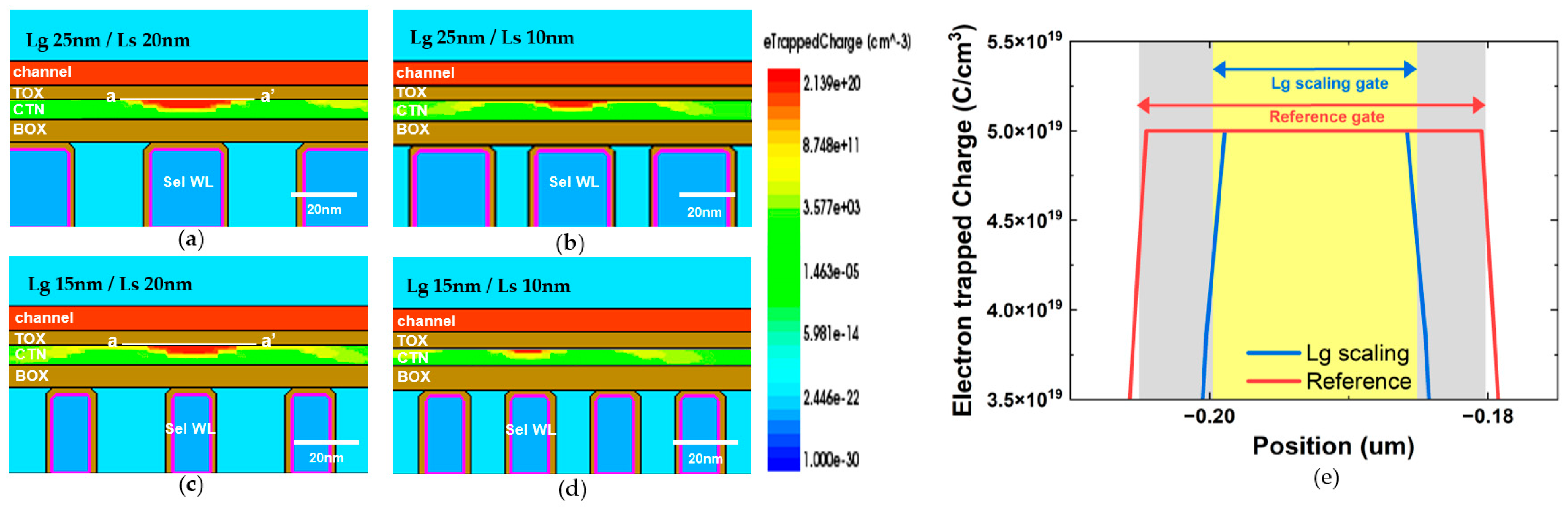
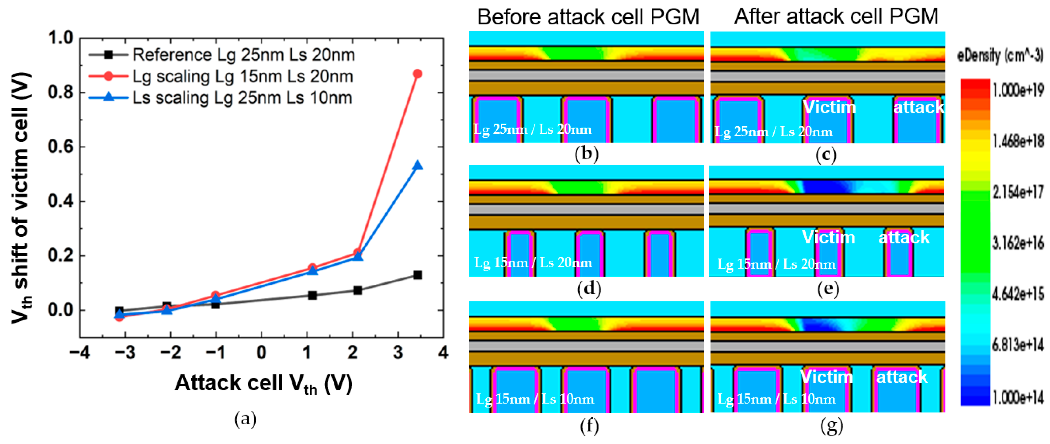
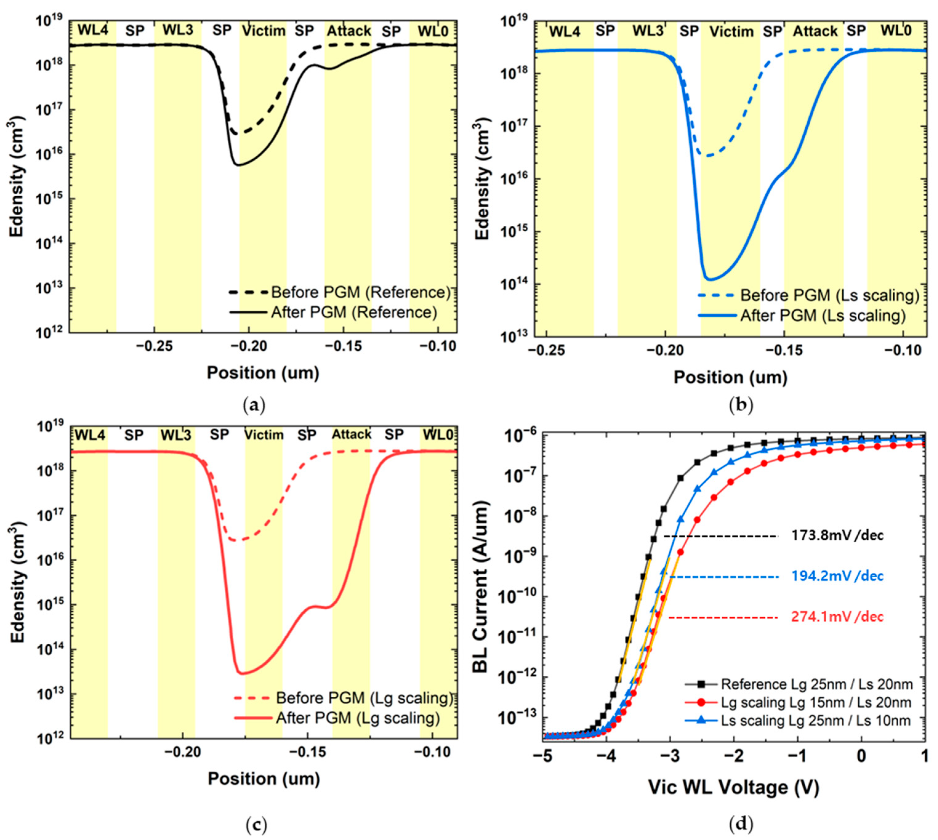
4. Investigation of Z-Interference

Figure 9a shows the Z-interference characteristics, indicating the amount of change in the victim cell Vth according to the change in the attack cell Vth for each structure. The results show that the Z-interference characteristics deteriorate exponentially when the attack cell Vth is programmed to 2 V or more during Ls and Lg scaling compared to the reference. Additionally, the amount of Z-interference degradation is greater during Lg scaling compared to Ls scaling.
To determine the cause of these changes, we examined the change in electron density within the poly-Si channel before and after programming the attack cell for each structure, as shown in Figure 9b–g. The results indicate that the decrease in electron density in the lower part of the WL before and after the attack cell programming is much larger during Lg scaling compared to Ls scaling.
Figure 10a–c quantitatively compare the electron density before and after the attack cell program by cutting the poly-Si channel area in Figure 9b–g. The results reveal that the electron density in the victim cell and spacer area decreases by more than 10 times during Lg scaling compared to Ls scaling. To analyze this cause, we checked the Id-Vg curve of the victim cell after the attack cell program for each device, as shown in Figure 10d. The results indicate that the change in sub-threshold swing (SS) characteristics of each device varies significantly depending on the attack cell program. Notably, the amount of SS deterioration is much larger during Lg scaling compared to Ls scaling, which is interpreted as a more severe deterioration of gate controllability during Lg scaling.
In general, the Z-interference characteristic tends to improve as the gate-to-substrate controllability of the selected WL increases [11]. Therefore, a large SS on the Id-Vg of the selected WL implies weak gate controllability, which suggests greater vulnerability to Z-interference characteristics. Thus, it can be inferred that the deterioration of gate controllability during Lg scaling compared to Ls scaling further accelerates the deterioration of Z-interference.
Additionally, this phenomenon of gate controllability deterioration can be indirectly confirmed by comparing the tendency of initial Vth reduction in Figure 2a. The Vth roll-off phenomenon due to SCE is more noticeable during Lg scaling compared to Ls scaling. This decrease in the Vth indicates a weakening of gate controllability [15]. Moreover, a large initial Vth reduction means that a larger amount of electrons must be stored when programming an attack cell to achieve the same programmed Vth value. This change is thought to be the cause of additional Z-interference degradation during Lg scaling.

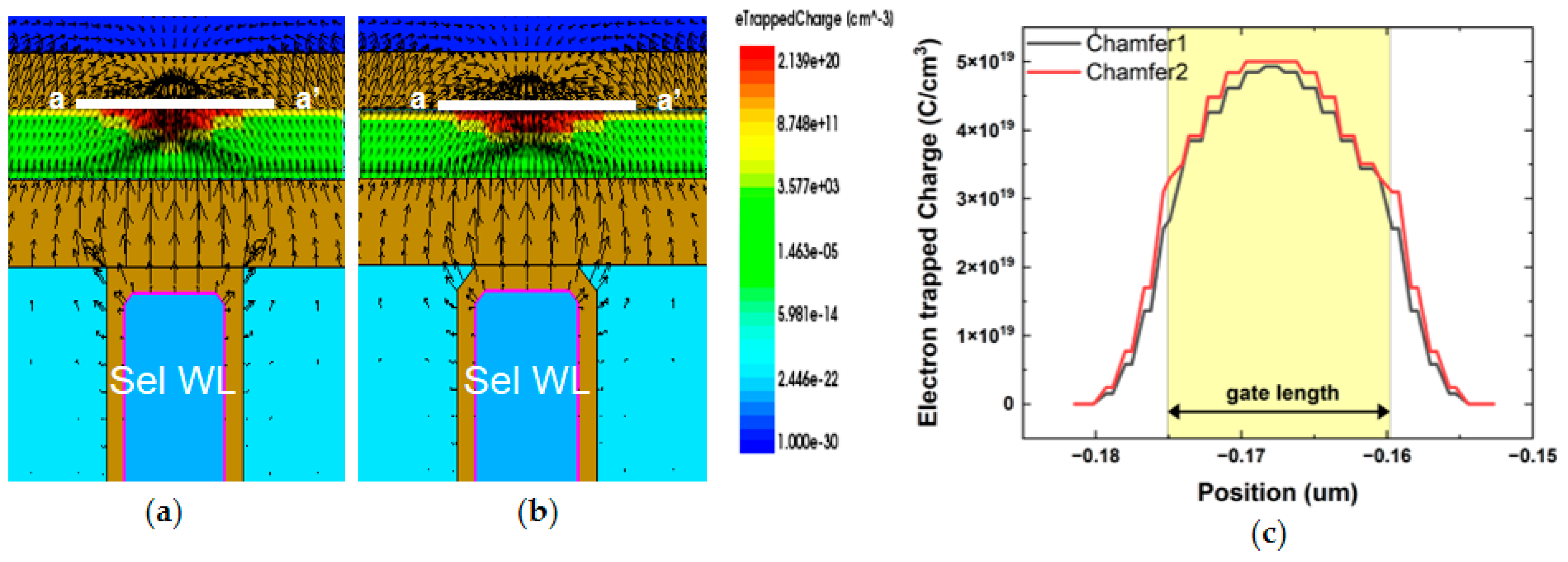
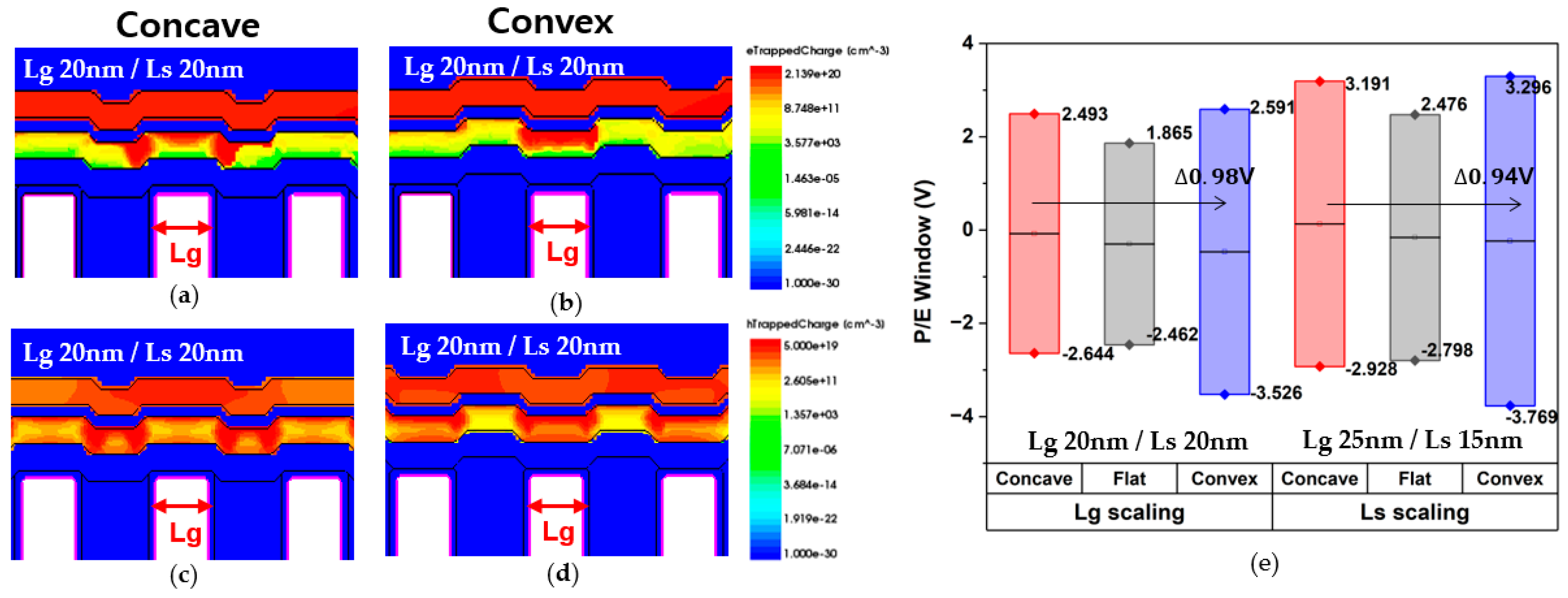
5. The Effect of Concave and Convex Structures

In terms of a vertical cross-section, 3D NAND flash memory involves depositing a gate dielectric and poly-Si channel after collectively etching channel holes, which can result in each WL having either a concave or convex structure [16]. Recent research has focused on maximizing memory characteristics by applying specific curvatures to the poly-Si channel. Based on studies showing that the shape of the poly-Si channel can alleviate program speed degradation in a channel structure with specific curvature, we analyzed memory window characteristics by applying concave and convex structures to each ON pitch reduction structure. Existing studies obtained significant results when the recess thickness, a variable related to channel curvature, was 3 nm or more [17]. Thus, in this study, the recess thickness was set to 3 nm for both convex and concave structures. The recess thickness is the physical parameter representing the curvature of the polysilicon channel layers. Additionally, to apply variables within a realistically applicable process range, the ON pitch was implemented by reducing Lg and Ls by 5 nm each in the reference device. Other doping and materials were set as identical to the simulation structures in Figure 1a–d.
Figure 11a–d show the electron and hole-trapped charge after program and erase operations in the concave and convex channel structures when Lg/Ls is 20 nm. The results show dense e-trapped charges in the charge trap layer of the selected WL region in the convex structure. In comparison, concave channels have a more widely distributed charge, showing similar results to previous studies on curvature channels [17]. This is likely because, as explained in previous studies, the electric field confined to the center of the gate in the concave structure is reduced, causing the trapped charge to form more widely. Additionally, compared to e-trapped charges, hole-trapped charges also have a higher concentration in the lower gate area in the convex structure than in the concave structure. However, even in the convex structure, where the electric field concentration is high at the bottom of the WL, it is confirmed that a high concentration of e-trapped charges is mainly formed only at the bottom of the gate, whereas a high concentration of h-trapped charges is formed in the space region. This variation in CTL regional concentration between electrons and holes can significantly deteriorate data retention characteristics in the lateral direction [16].
Figure 11e confirms the improvement in the program and erase window when using the convex structure compared to the concave structure when scaling Lg and Ls. The results show that the improvement in the PE window is much higher during Lg scaling compared to Ls scaling. This is likely because the reduced gate-to-substrate capacitive coupling caused by Lg scaling is compensated for by strengthening the electric field at the bottom of the gate in the convex structure. Therefore, using an appropriate level of channel curvature change in the convex direction to compensate for PE window deterioration during Lg scaling can be considered a very effective strategy.
Additionally, when applying the convex structure, the Z-interference degradation phenomenon can be further improved, as the electrons are confined only to the lower WL of the attack cell. However, if the convex structure is applied excessively, this may intensify the deterioration of retention characteristics, as described above. Therefore, considering the trade-off characteristics of the memory window and retention characteristics, it is essential to engineer a combination of Lg and Ls scaling to form an optimal reliability margin. Finally, since the various simulation results thus far are based on theoretical conditions, there may be some differences between the predicted results of this simulation and the actual outcomes due to process variability and material property uncertainties in the fabrication of 3D NAND devices. Additionally, the simulation model may not perfectly replicate the physical phenomena, making experimental validation crucial. Subsequent experiments are necessary to appropriately review the validity of the TCAD simulation data and to adjust and optimize it for actual processes.

6. Conclusions

This study systematically investigated the impact of ON pitch scaling and channel curvature on the performance of 3D NAND flash memory. By focusing on reducing the spacer length (Ls) and gate length (Lg), we aimed to improve the memory characteristics through detailed TCAD simulations. Our findings indicate that Lg scaling significantly affects the programmed threshold voltage (Vth) due to increased short channel effects (SCEs) and reduced capacitive coupling, whereas Ls scaling has a comparatively smaller impact. Additionally, the analysis revealed that Z-interference characteristics deteriorate more with Lg scaling compared to Ls scaling primarily due to weaker gate controllability. We also examined the effects of concave and convex channel structures on memory performance. The results demonstrate that convex channels improve the program speed and mitigate Z-interference by confining trapped charges more effectively, although excessive curvature may lead to retention characteristic deterioration. Overall, this research provides important insights into optimizing the trade-offs between the memory window and retention characteristics. By systematically analyzing the effects of Ls and Lg scaling and channel curvature, we offer valuable guidelines for enhancing the reliability and performance of 3D NAND flash memory. These findings can inform future developments in memory technology, ensuring better performance and reliability in increasingly dense and complex 3D NAND flash based-storage systems.

Author Contributions

Conceptualization, J.K.P.; methodology, J.K.P.; software, H.Y.B.; validation, S.K.H.; formal analysis, H.Y.B. and S.K.H.; investigation, H.Y.B.; writing—original draft preparation, H.Y.B.; writing—review and editing, J.K.P.; visualization, H.Y.B.; supervision, J.K.P.; project administration, J.K.P.; funding acquisition, J.K.P. All authors have read and agreed to the published version of the manuscript.

Funding

This study was supported by the Research Program funded by SeoulTech (Seoul National University of Science and Technology).

Institutional Review Board Statement

Not applicable.

Informed Consent Statement

Not applicable.

Data Availability Statement

The original contributions presented in the study are included in the article, further inquiries can be directed to the corresponding author.

Conflicts of Interest

The funders had no role in the design of the study; in the collection, analyses, or interpretation of data; in the writing of the manuscript; or in the decision to publish the results.

References

  1. Jun, H.; Cho, J.; Lee, K.; Son, H.-Y.; Kim, K.; Jin, H.; Kim, K. Hbm (high bandwidth memory) dram technology and architecture. In Proceedings of the 2017 IEEE International Memory Workshop (IMW), Monterey, CA, USA, 14–17 May 2017; pp. 1–4. [Google Scholar]
  2. Park, K.-T.; Han, J.-M.; Kim, D.; Nam, S.; Choi, K.; Kim, M.-S.; Kwak, P.; Lee, D.; Choi, Y.-H.; Kang, K.-M.; et al. 19.5 Three-dimensional 128Gb MLC vertical NAND Flash-memory with 24-WL stacked layers and 50MB/s high-speed programming. In Proceedings of the 2014 IEEE International Solid-State Circuits Conference Digest of Technical Papers (ISSCC), San Francisco, CA, USA, 9–13 February 2014. [Google Scholar]
  3. Goda, A.; Parat, K. Scaling directions for 2D and 3D NAND cells. In Proceedings of the 2012 International Electron Devices Meeting, San Francisco, CA, USA, 10–13 December 2012; pp. 2.1.1–2.1.4. [Google Scholar]
  4. Spinelli, A.; Compagnoni, C.; Lacaita, A. Reliability of NAND Flash Memories: Planar Cells and Emerging Issues in 3D Devices. Computers 2017, 6, 16. [Google Scholar] [CrossRef]
  5. Goda, A. 3-D NAND technology achievements and future scaling perspectives. IEEE Trans. Electron Devices 2020, 67, 1373–1381. [Google Scholar] [CrossRef]
  6. Alsmeier, J.; Higashitani, M.; Paak, S.S.; Sivaram, S. Past and Future of 3D Flash. In Proceedings of the 2020 IEEE International Electron Devices Meeting (IEDM), San Francisco, CA, USA, 12–18 December 2020. [Google Scholar]
  7. Nam, K.; Park, C.; Yoon, J.-S.; Jang, H.; Park, M.S.; Sim, J.; Baek, R.-H. Origin of incremental step pulse programming (ISPP) slope degradation in charge trap nitride based multi-layer 3D NAND flash. Solid-State Electron. 2021, 175, 107930. [Google Scholar] [CrossRef]
  8. Chen, W.-C.; Lue, H.-T.; Hsiao, Y.-H.; Hsu, T.-H.; Lin, X.-W.; Lu, C.-Y. Charge storage efficiency (CSE) effect in modeling the incremental step pulse programming (ISPP) in charge-trapping 3D NAND flash devices. In Proceedings of the 2015 IEEE International Electron Devices Meeting (IEDM), Washington, DC, USA, 7–9 December 2015. [Google Scholar]
  9. Sim, J.-M.; Kang, M.; Song, Y.-H. A Novel Program Operation Scheme with Negative Bias in 3-D NAND Flash Memory. IEEE Trans. Electron Devices 2021, 68, 6112–6117. [Google Scholar] [CrossRef]
  10. Chang, Y.-W.; Wu, G.-W.; Yang, I.-C.; Huang, Y.-H.; Lee, Y.-J.; Chen, K.-F.; Chen, Y.-J.; Lu, T.-C.; Chen, K.-C.; Lu, C.-Y. Deteriorated Non-Linear Interference in 3D NAND Cell with Word-Line Pitch Scaling Due to the Incapability to Turn on Non-Gate-Controlled Region. IEEE Electron Device Lett. 2023, 44, 1837–1840. [Google Scholar] [CrossRef]
  11. Kim, Y.; Hong, S.K.; Park, J.K. Optimizing Confined Nitride Trap Layers for Improved Z-Interference in 3D NAND Flash Memory. Electronics 2024, 13, 1020. [Google Scholar] [CrossRef]
  12. Rachidi, S.; Arreghini, A.; Verreck, D.; Donadio, G.; Banerjee, K.; Katcko, K.; Oniki, Y.; Rosmeulen, M. At the Extreme of 3D-NAND Scaling: 25 nm Z-Pitch with 10 nm Word Line Cells. In Proceedings of the 2022 IEEE International Memory Workshop (IMW), Dresden, Germany, 15–18 May 2022; pp. 1–4. [Google Scholar]
  13. Kim, C.; Kim, D.H.; Jeong, W.; Kim, H.J.; Park, I.H.; Park, H.W.; Lee, J.; Park, J.; Ahn, Y.L.; Lee, J.Y.; et al. A 512Gb 3b/cell 64-Stacked WL 3D V-NAND Flash Memory. IEEE J. Solid-State Circuits 2017, 53, 124–133. [Google Scholar] [CrossRef]
  14. Kim, S.; Shin, H. Analysis of the Effect of Residual Holes on Lateral Migration During the Retention Operation in 3-D NAND Flash Memory. IEEE Trans. Electron Devices 2021, 68, 6094–6099. [Google Scholar] [CrossRef]
  15. Chaudhry, A.; Kumar, M.J. Controlling short-channel effects in deep-submicron SOI MOSFETs for improved reliability: A review. IEEE Trans. Device Mater. Reliab. 2004, 4, 99–109. [Google Scholar] [CrossRef]
  16. Park, S.; Lee, J.; Jang, J.; Lim, J.K.; Kim, H.; Shim, J.J.; Yu, M.-t.; Kang, J.-K.; Ahn, S.J.; Song, J. Highly-reliable cell characteristics with 128-layer single-stack 3D-NAND flash memory. In Proceedings of the 2021 Symposium on VLSI Technology, Kyoto, Japan, 13–19 June 2021; pp. 1–2. [Google Scholar]
  17. Song, J.; Sim, J.-M.; Kim, B.; Song, Y.-H. Concave and Convex Structures for Advanced 3-D NAND Flash Memory Technology. IEEE Trans. Electron Devices 2024, 71, 2810–2814. [Google Scholar] [CrossRef]
Figure 1. Simulated structures. (a) Reference structure, (b) Ls scaling, (c) Lg scaling, and (d) both Lg and Ls scaling. (e) Corresponding simulated parameters of reference structure.
Applsci 14 06689 g001
Figure 2. (a) Initial Vth and programmed Vth of selected WL under various Lg and Ls scaling conditions. (b) Difference between programmed Vth and initial Vth under various Lg and Ls scaling conditions.
Applsci 14 06689 g002
Figure 3. Electron-trapped charge distribution in charge trap layer during program operation in (a) reference, (b) Lg scaling, (c) Ls scaling, and (d) both Lg/Ls scaling. (e) Comparison of e-trapped charge in CTL by cutting a-a’ area in (a,b).
Applsci 14 06689 g003
Figure 4. Electric field and e-trapped charge distribution in CTL during program operation in (a) perfect right-angle structure; (b) structure with 2 nm rounded edges. (c) Comparison of e-trapped charge in CTL by cutting a-a’ area in (a,b).
Applsci 14 06689 g004
Figure 5. (a) E-trapped charge distribution when program voltage is 17 V in reference and Ls scaling. (b) Comparison of e-trapped charge in CTL by cutting a-a’ area in (a,b). (c) Comparison of electric field in gate stacks by cutting b-b’ area in (a,b). (d) Programmed Vth as function of program voltage in reference and Ls scaling structure. (e) E-trapped charge distribution when program voltage is 22 V in reference and Ls scaling. (f) Electron density of poly-Si channel during read operation when programmed Vth is high (4.4 V) and low (0 V).
Applsci 14 06689 g005
Figure 6. (a) Initial Vth and erased Vth of selected WL under various Lg and Ls scaling conditions. (b) Difference between erased Vth and initial Vth under various Lg and Ls scaling conditions.
Applsci 14 06689 g006
Figure 7. Hole-trapped charge distribution in CTL during erase operation in (a) reference, (b) Ls scaling, and (c) Lg scaling. (d) Comparison of h-trapped charge in CTL by cutting a-a’ area in (ac).
Applsci 14 06689 g007
Figure 8. Program and erase window of selected WL under various Lg and Ls scaling conditions.
Applsci 14 06689 g008
Figure 9. (a) Comparison of Z-interference in reference, Lg scaling, and Ls scaling structures. Change in electron density within poly-Si channel before and after programming attack cell in (b,c) reference, (d,e) Lg scaling, and (f,g) Ls scaling structures.
Applsci 14 06689 g009
Figure 10. Comparison of electron density before and after the attack cell program by cutting poly-Si channel area in Figure 9b–g in case of (a) reference, (b) Ls scaling, and (c) Lg scaling. (d) Id-Vg curve of victim cell after attack cell program for each device.
Applsci 14 06689 g010
Figure 11. Electron-trapped charge after program operations in (a) concave and (b) convex channel structures and hole-trapped charge after erase operations in (c) concave and (d) convex channel structures when Lg/Ls is 20 nm. (e) P/E window according to channel curvature change in both Lg and Ls scaling.
Applsci 14 06689 g011
Table 1. Simulated voltage condition.
ProgramEraseRead
Selected cell17~18 V0 V−5 V~5 V
Unselected cell5.5 V0 V5.5 V
BL0 V20 V0.5 V
DSL3.3 VFloating3.3 V
SSL0 VFloating3.3 V
SL2 V20 V0 V
Disclaimer/Publisher’s Note: The statements, opinions and data contained in all publications are solely those of the individual author(s) and contributor(s) and not of MDPI and/or the editor(s). MDPI and/or the editor(s) disclaim responsibility for any injury to people or property resulting from any ideas, methods, instructions or products referred to in the content.

