Article

Silicon Surface Nanostructuration with Symmetric Cathode Configurations for Photonic Devices

by
Rehab Ramadan
1,2,*,
Mahmoud Hamdy Elshorbagy
1,3 and
Raúl J. Martín-Palma
2,4
1
Department of Physics, Faculty of Science, Minia University, El-Minya 61519, Egypt
2
Departamento de Física Aplicada, Universidad Autónoma de Madrid, Campus de Cantoblanco, 28049 Madrid, Spain
3
Applied Optics Complutense Group, Optics Department, Faculty of Optics and Optometry, Universidad Complutense de Madrid, Arcos de Jalón, 118, 28037 Madrid, Spain
4
Instituto Universitario de Ciencia de Materiales “Nicolás Cabrera”, Universidad Autónoma de Madrid, Campus de Cantoblanco, 28049 Madrid, Spain
*
Author to whom correspondence should be addressed.
Appl. Sci. 2024, 14(19), 8635; https://doi.org/10.3390/app14198635
Submission received: 21 August 2024 / Revised: 18 September 2024 / Accepted: 23 September 2024 / Published: 25 September 2024
(This article belongs to the Section Nanotechnology and Applied Nanosciences)

Abstract

:
The physical properties of porous silicon (PSi) can be adjusted to provide a better performance in optoelectronic devices. A controlled method commonly used to fabricate PSi is the anodization process, which employs platinum as a conventional cathode. Herein, we investigate the effect of replacing the Pt cathode with symmetric heavily doped silicon on the resulting surface structure on silicon substrates. The symmetric configuration is established when both anode and cathode are from the same material. Three different samples were anodized using both configurations and under different fabrication conditions. The results demonstrate the possibility to produce porous silicon structure using the heavily doped Si as alternative to the expensive Pt counter electrode. Furthermore the modified configuration offers the possibility of manufacturing large areas of nanostructured PSi without limitation of the counter electrode area and the applied current density. The formed porous structures using Si cathode have better uniformity, larger pore size, and lower number of interlinked and shallow holes than traditional methods. The porous structures fabricated with this configuration show broadband reduction in spectral reflectivity and changes in the schottky diode dark characteristics when compared with PSi fabricated with Pt conventional electrode.

1. Introduction

Besides bulk processing, the physicochemical properties of silicon can be customized for specific applications by altering its surface [1]. Porous silicon (PSi) is a highly adaptable material with diverse applications, especially in the biomedical and photonics fields [2,3]. Its utility stems from its ability to be easily adjusted to meet specific electrical, optical, and thermal requirements [4,5]. For instance, several sensing devices leverage the optical and electrical properties of PSi to detect variations in chemical and biological samples [6], including even minute changes in gas molecules through surface modifications [7].
In photonics, PSi is incorporated into gamma ray detectors [8], photonic crystals [9,10], and waveguides [11]. The characteristic photoluminescence and efficient light trapping capabilities of PSi make it ideal for use in next-generation solar cells and photodetectors [12,13,14,15].
There are several effective techniques for creating porous silicon, including metal-assisted chemical etching [16], reactive ion etching [17], the sulfur-template method [18], metal-assisted electrochemical etching [19], and electroless chemical etching [20]. Most of these methods rely on dry etching or electrochemical processing [1]. Dry etching requires a hard mask to define the pore structure, whereas electrochemical methods use hydrofluoric solutions and an external power source to drive the reaction [21]. Since the first discovery of PSi in 1950s [22], there is an intensive research efforts to investigate the effect of each parameter of the electrochemical process of silicon surface [23,24,25]. The electrochemical process can be fine-tuned by adjusting the etching current density (J), etching time (t), temperature, and electrolyte composition [3,23]. The main advantage of this process is the ability to produce porous silicon using a diluted electrolyte of hydrofluoric acid (HF) [23].
The parameters of the electrochemical process can be divided into two main categories, the electrical and chemical parameters [26]. The chemical part of the process include the mix of hydrofluoric acid (HF) with other solvents such as ethanol (ETOH) and dimethylformamide (DMF). The concentration and percent of each solvent are the main parameters for this mixture [27]. Focusing on the electrical parameters, we found that the anode and cathode type and their shapes greatly affect the current distribution on the substrate surface and result in diverse nano/micro structures [28,29]. In this aspect, the conventional electrochemical reaction setup has the following design: counter electrode (metal)/electrolyte/working electrode (substrate). If the substrate is from a poor conductive material, such as silicon, we apply an ohmic contact to enhance the electrochemical reaction. Then, the final setup becomes as follow: metal/electrolyte/substrate/metal. When applying this configuration to silicon substrates, the electrolyte typically consists of an HF solution. As a result, the cathode material must be an inert metal that can withstand this corrosive acid. This resulted in limited options for the cathode material, with platinum (Pt) as conventional choice [24,30]. Consequently, the fabrication on large scale is limited because of the high cost of Pt electrodes. Exploring alternatives for this crucial component of the electrochemical cell could enable scalable and cost-effective fabrication of these layers. Moreover, it could result in variations in the characteristics of the fabricated layers. Scaleable fabrication, cost-efficiency, and structural variations all have an impact on the physical properties of PSi and its potential applications.
Current work presents a cost-effective modification in the electrochemical etching process that can produce a large area nanostructured PSi layer with better uniformity. The main idea is to employ heavily doped silicon wafers as a counter electrode instead of expensive Pt wires to have a symmetric anode/cathode setup in the form: Al/Si/electrolyte/Si/Al. With this setup only silicon surface is exposed to the electrolyte through the holders aperture. With the electrical driven chemical etching the anode surface converted to nanostructure while maintain the cathode surface at minimum etching rate. Following the brief introduction, Section 2 provides detailed information about the fabrication setup and materials. In Section 3, we present the morphology, optical, and electrical analysis of the fabricated samples. While a general conclusions are summarized at the last section.

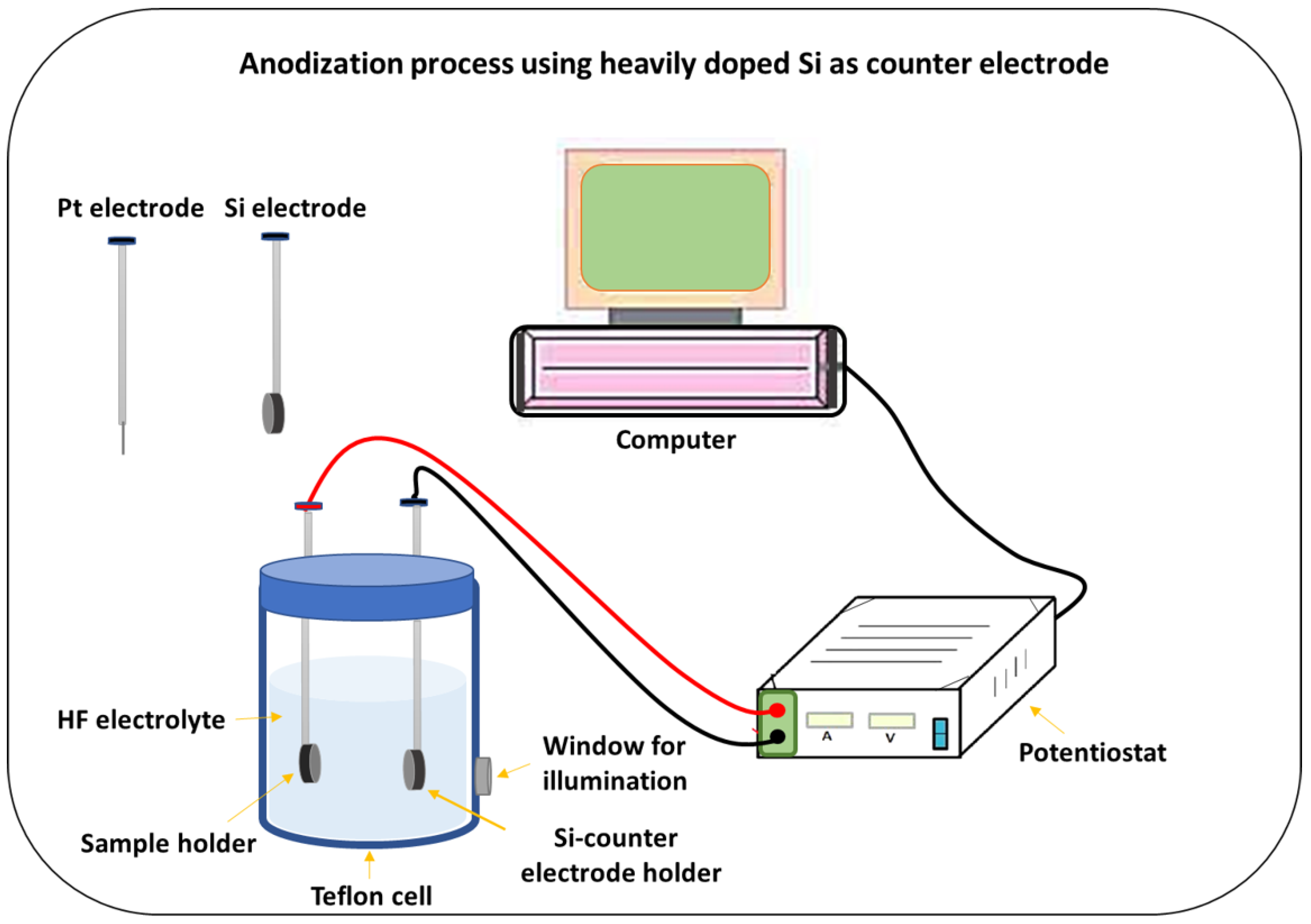
2. Materials and Methods

The porous layers were fabricated on the surface of one side polished boron-doped p-type crystalline silicon wafers (surface roughness of the order of 0.1 nm), with orientation <100>. The anodization method was employed to grow porous structures on the polished side, while the other side, coated with aluminum (Al) via electron beam evaporation, serves as the bottom contact. For Al evaporation, the base pressure was 1.25 × 10⁻⁵ mbar and the evaporation time was 4 min, resulting in 150 nm-thick Al thin films, measured by the machine thickness monitor. The Al thin films were subsequently annealed by rapid thermal processing (RTP) in nitrogen atmosphere for 5 min to turn the initial rectifying behavior into ohmic. The silicon samples with an area of 1.5 × 1.5 cm2 were mounted in Teflon holder with a circular aperture of 1.23 cm2. The electrolyte for each case is a mix from HF and ETOH or DMF. The samples properties and the anodization parameters are summarized in Table 1.
Before the etching process, the substrate was cleaned by immersing it in ethanol to remove any organic contamination, then rinsed with water and dried. The fabrication process of the experimental setup is schematically described in Figure 1. The intended samples were etched using the conventional Pt and heavily doped Si wafer ( ρ s = 0.01–0.02 Ω·cm) as counter electrodes. The geometry and electrode type has some effects on the fabricated structure. The geometry of Pt electrode is a wire with 1mm diameter, forming the following setup: Pt/electrolyte/Si/Al with none symmetric conductivity surfaces exposed to the electrolyte. While the heavily doped Si with the same area and holder aperture used in the second case form the following setup: Al/Si/electrolyte/Si/Al with symmetric conductivity surfaces exposed to the electrolyte. The anodization cell were controlled using potentiostat with constant current mode. Two etching current density values were used for both cell setups to form different nanostructured surface on silicon samples namely 20 mA/cm2 and 80 mA/cm2. The selection of the time and the etching current density depends on the resistivity of Si substrate [31,32,33,34]. In the case of low doped silicon ( ρ s = 25–30 Ω·cm) we used illumination with halogen lamp (60 W) through a window in the Teflon cell to facilitate the etching process by activating the carriers [34,35]. After the fabrication process, each sample was rinsed with ethanol, followed by deionized water and finally dried with a mild stream of dry nitrogen.
The morphology of the PSi layers was studied by field emission scanning electron microscope (FESEM- XL-40 FEG, Philips, Eindhoven, Netherlands). An energy dispersive spectroscopy X-ray analyzer (EDS, Inca X-sight 7558, Oxford Instruments, London, UK) coupled to the microscope was used to determine the elemental compositions of the samples. The Optical characterization in the UV-visible range (250–900 nm) was performed using a Jasco V-560 double-beam spectrophotometer equipped with an integrating sphere to avoid scattering losses. For insight comparison we select the samples with small pores sizes (S1) for the electrical characterization, An Au circular top contact was deposited using DC sputtering technique on the surface of the PSi layer. The deposition was performed in an argon atmosphere through a patterned mask. The deposition pressure was 2 × 10 2 mbar, and the plasma current was 20 mA, resulting in a thickness of ≈50 nm. The final structure of the fabricated Schottky devices is Al/Si/PSi/Au. The electrical characterization of this junction was carried out using a Bio- Logic SP-150 potentiostat with a scan rate of 5 mV/s and an applied potential in the range of +1.0 to −1.0 V. A homemade cell, which consisted of two movable copper probes with a diameter of 0.5 mm and a copper base (2 × 2 cm2), was utilized for the measurements. The measurements were conducted in a Faraday box to shield them from any external signals.

3. Results and Discussion
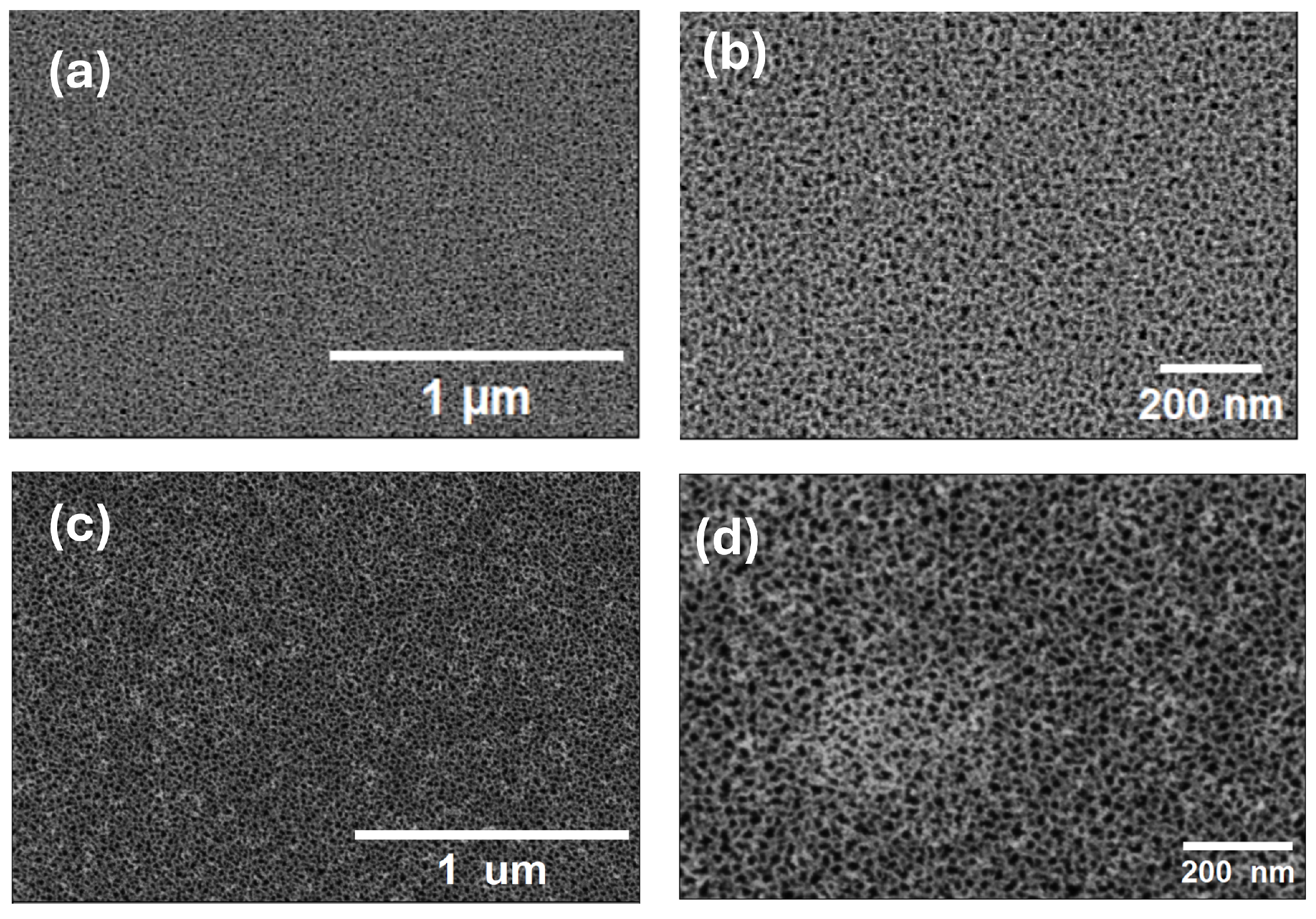
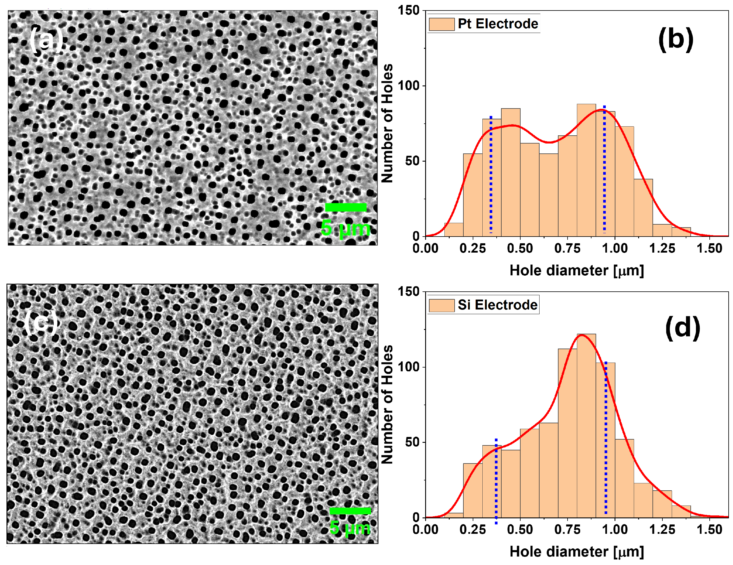
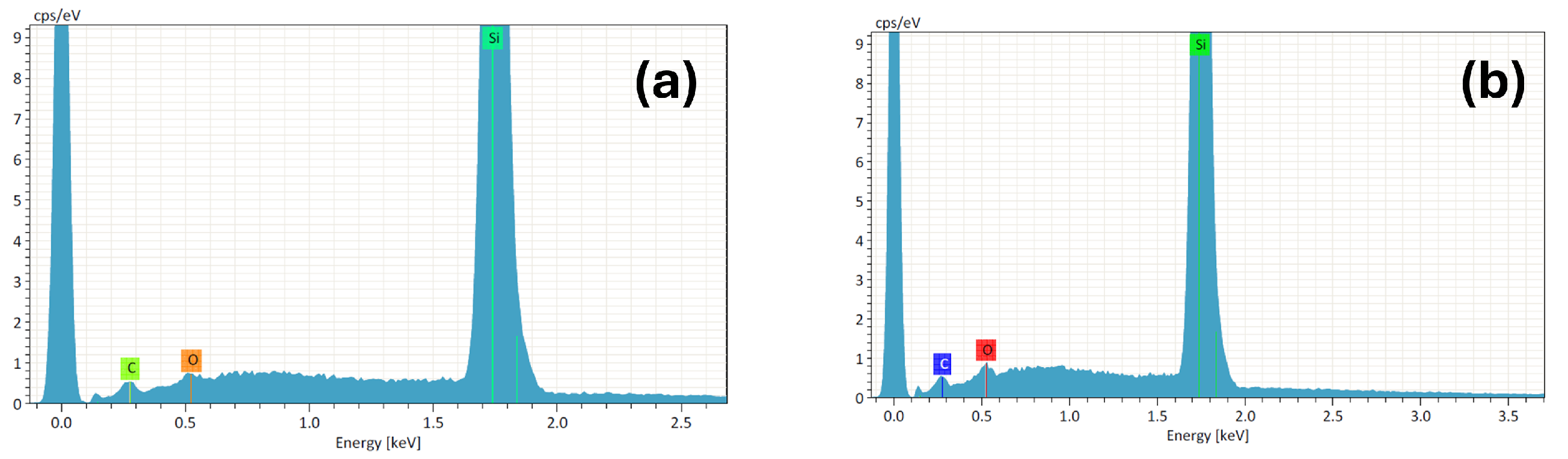
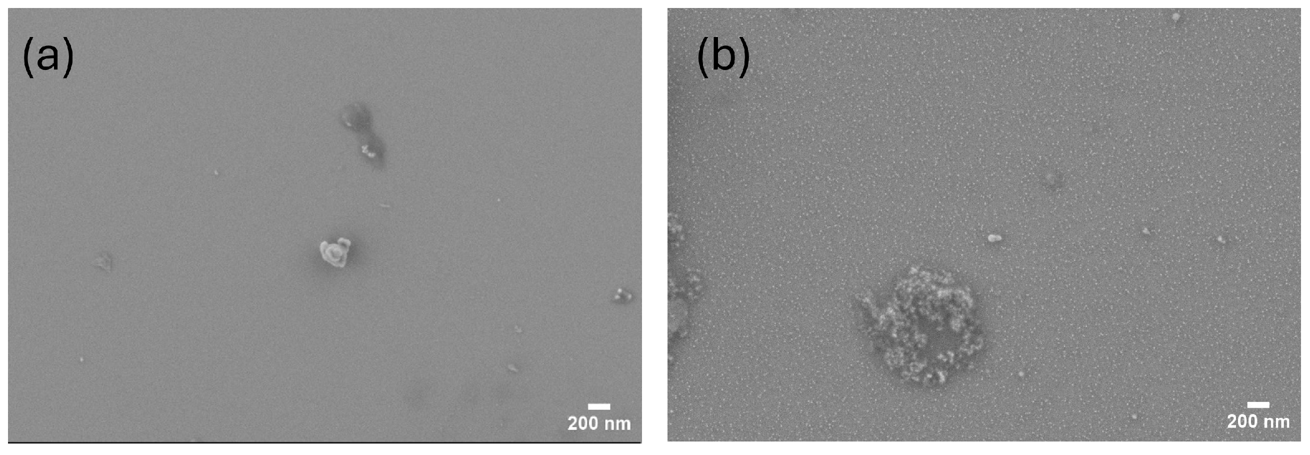
3.1. Morphology

It is imperative to note that the morphology of electrochemically etched PSi layers is highly reliant on the fabrication parameters, such as anodization current density, temperature, and HF concentration, among others. Here, we investigate an additional parameter that reveals diverse changes in the silicon surface structure, namely the cathode type. The new cathode configuration and the conventional Pt cathode configuration applied to three different substrate (silicon with different doping levels) to check the global and specific changes in the PSi samples in both setups. Comparison between PSi samples prepared on teh suface of S1 substrate using the Pt and Si electrodes are shown in Figure 2, highlighting the morphology and homogeneity of the nanstructured PSi layer.
As portrayed in Figure 2b for the Pt cathode case the pore size appears to be smaller than those in Figure 2d for the symmetric silicon cathode case. The size of PSi in this sample is quite small, therefore, further analysis of size and distribution is difficult and will not be accurate. More reasonable analysis for size distribution is performed on sample with larger pores size to provide quantitative analysis for pore size and distribution. The first samples S1 reveals in both setups a nanoporous silicon surface (see Figure 2) with quite small pore size in the range of 20–40 nm. It is worth noting that this type of heavily doped silicon is used in photodetectors, then nanoporous surface maybe benefit to confine light at short wavelengths at nanoscale. Although silicon cathode has a higher resistivity when compared with Pt, these images show the successful fabrication of PSi layers using both configurations. The next step is to check the effect of substrate type and electrolyte on the fabricated sample. In each step, we maintain consistent fabrication conditions across both setups for the purpose of comparison. While additional fabrication sets could reveal a range of diverse structures and morphologies, the three selected cases are sufficient to introduce the concept and examine the effects of the Si cathode type.
A quite interesting microstructure surface obtained for the silicon samples S2, namely microflakes and spongy structures (see Figure 3). At large scales (tens of microns) the surface of the sample produced using the Pt electrode looks as a sponge with randomly distributed large holes as in Figure 3a, once we down to the nanoscale a clear spongy surface appears with tiny holes of few nanometers (see Figure 3b,c). Different from this case, the sample produced with the symmetric Si cathode show a surface with microflakes on top as we can see in Figure 3d. At the nanoscale, a spongy surface is visible beneath the microflakes (see Figure 3e,f), resulting in a bilayer surface structure. Although both samples show some uniformity at the microscale, they appear quite random at the nanoscale. In general, porous silicon (PSi) is effective at trapping light, which leads to a reduction in reflectance [36]. Certainly, this microflake structure will lead to a further reduction in reflectivity, as confirmed in the final section of the optical characterization.
A comprehensive analysis of the pore size distribution was conducted for the samples fabricated on S3 substrate. The average pore size of these samples is approximately one micron, making it clear and straightforward to analyze. We used imageJ software (version 1.54g) to count the pore size and distribution in a total analysis area of 44 × 31 = 1396.11 μ m2. The SEM image and their pore size distribution are shown in Figure 4. In Figure 4b, the pore size show a wide plateau and high dispersion in size of image in Figure 4a, indicating low uniformity. The total holes area 316.011 μ m2, this reveals porosity of 22.6% with total number of holes as 707 mostly distributed in a plateau between 330–950 nm.
Another observation from this SEM image is the presence of a large number of shallow and interlinked holes. Moving to the micropores produced by the symmetric silicon cathode in Figure 4c, and its pore size analysis in Figure 4d, we can see that the total area of the holes is 344.3 μ m2, that gives a porosity of 24.68%. Although the total number of holes (694 for this image) and porosity are not so different from the Pt sample, the size distribution is notably different where most of the hole diameters are concentrated around 829 nm. This indicate a more uniform distribution compared with the Pt sample. The number of shallow and interlinked holes is fewer for the symmetric cathode sample. In this third sample we continue to explore the potential of using a Si substrate as cathode in the fabrication of PSi layers and assess its impact on the pore size. As a conclusion, the morphology analysis reveals that using silicon as cathode produce a more uniform and larger pore size distribution, both for nanoscale and microscale sizes. Using certain fabrication parameters and sample type silicon cathode can produce bilayer structure with microflakes/spongy form.
It is important to examine the surface composition of the samples. To this end, we selected the S1 substrate samples for EDS analysis. The results shown in Figure 5a, for the Pt electrode sample and Figure 5b, for the Si electrode sample, where both reveal almost the same composition. Which indicates that we have only a structural modification rather composition changes. We thoroughly examined the morphology of the Si substrate used as a counter electrode after multiple uses in the etching process. The durability of the Si cathode is an important criteria to provide an effective alternative to the inert Pt electrode.
To the naked eye, the Si substrate appears unchanged before and after the anodization process. However, SEM image is a better tool to confirm the maintain of the substrate surface without critical damage. Figure 6 demonstrates the stability of the surface morphology of the used Si electrode. the SEM image for the silicon substrate before anodization in Figure 6a show a smooth surface without any nanofeatures, while that in Figure 6b for the substrate after anodization show a similar surface with some particulates on the surface. This nano roughness on the surface of Si substrate used as cathode can be a result of multiple insertions of the substrate into diluted HF electrolyte. This remarkable stability can be attributed to the minimal impact of the applied current density and short etching time on the Si electrode.

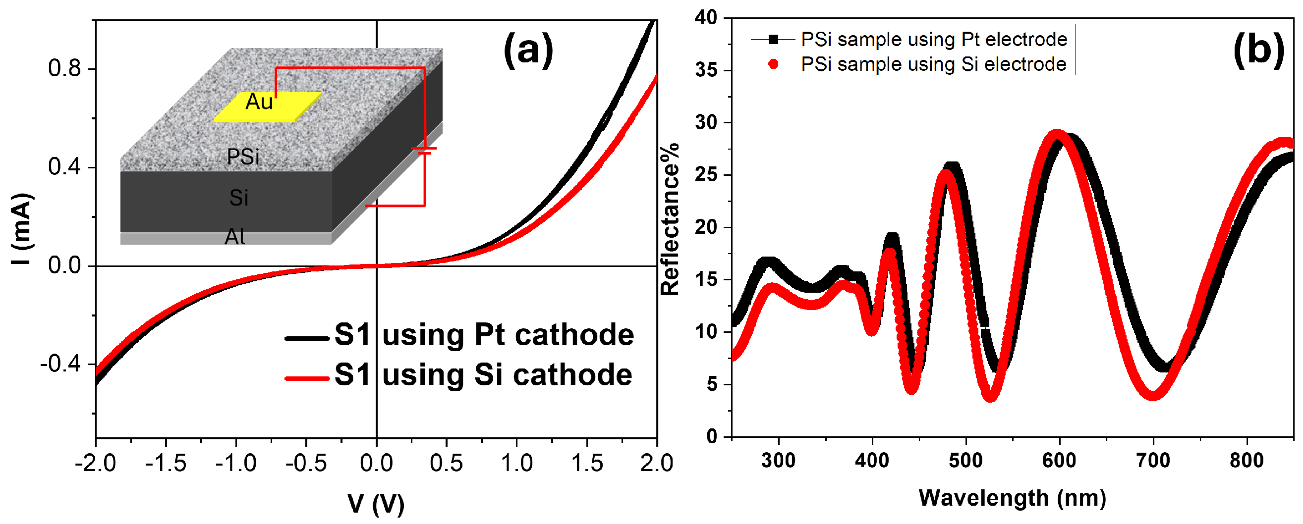
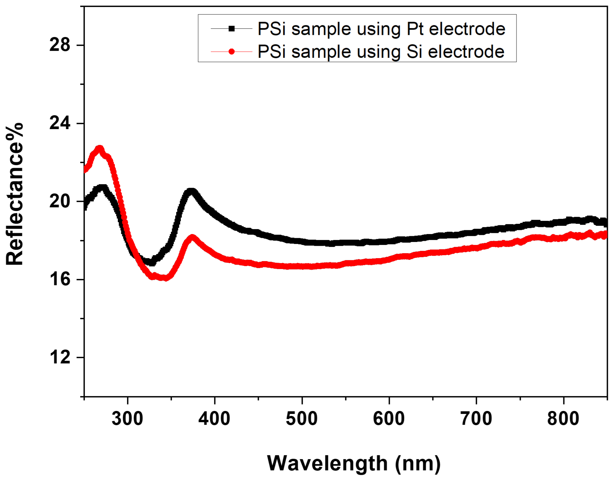
3.2. Optical and Electrical Properties

PSi layers are proposed for optoelectronic applications, so it is straightforward to examine the effect of the modification on the setup on the parameters of a semiconductor junctions. The simple form of these junctions is the ideal diode, for which the current and voltage are related using the following equation [37]:
I D = I 0 e x p q V n K B T 1
where ID is the dark current, I0 is the reverse saturation current, n is the diode ideality factor, kB is Boltzmann constant, and T is the absolute junction temperature. The ideal diode equation assumes that all recombination processes occur via band to band transitions or through traps in the bulk of the device. However, recombination could occur in other areas of the device, leading to losses in the overall performance of the diode. As such, a modified equation used for non-ideal diodes is given by the expression [37]:
I D = I 0 e x p q V n K B T 1 + V I R s R s h
Large values of Rs cause power to be dissipated in solar cells, while low Rsh leads to power losses by providing an alternate current path for the light-generated current. The current - voltage lines for junction of both samples produced by Pt and Si electrodes on S1 substrate are shown in Figure 7a, where the inset is a schematic of the fabricated schottky junctions. The fitting of these two lines to the non ideal diode equations reveals a slight differences in the diode characteristics in each case. The measured electrical parameters confirm that the fabricated junctions are suitable as Schottky diodes for use in optoelectronic devices.
A slight variation in the electrical parameters was observed between the samples prepared with Pt and Si counter electrodes. However, the ideality factor (n) is lower in the case of the device based on the Si electrode during the etching process of the PSi layer. This finding confirms the improvement in the homogeneity and uniformity of the fabricated PSi layers when using an asymmetric electrode, as confirmed by SEM analysis. All parameters are summarized in Table 2. The optical and electrical properties of PSi layers change at different levels of porosity [38,39,40]. A detailed analysis of these characteristics established the correlation between morphology, porosity, and electrical properties of PSi layers anodized using a Pt electrode. As a conclusion a PSi layer consists of air, amorphous silicon, silicon nanocrystals, and silicon dioxide [41,42]. These components are greatly influenced by the structure and porosity of the fabricated layer. The SEM images (see Figure 2, Figure 3 and Figure 4) revealed that the pore size increases in the case of PSi layers fabricated using a symmetric Si electrode. This indicates that the porosity of PSi layers increases when a symmetric electrode is used when compared with samples fabricated using Pt electrode under the same anodization conditions. Consequently, the resulting current is reduced at the same applied voltage for sample S1 prepared using a symmetric Si cathode, as shown in Figure 7a. The decrease in the electrical conductivity at higher porosity is linked to the widening of the band gap of the PSi layer at higher porosity [43].
The porosity and size distribution of PSi layers have a significant impact on spectral reflectance of the samples [44], making it a popular choice for antireflective coatings in optoelectronic devices [2,45]. Reducing optical losses through reflection has a direct impact in improving the overall device performance with maintaing a good electrical conduction. In Figure 7b we can see a broadband reduction in the reflectivity of the sample produced by the Si symmetric cathode when compared with that fabricated using Pt electrode. Another interesting note is that the reflectance dips at the VIS-NIR region is blue shifted while that at the UV is red shifted. The reflectance dip at the UV region is attributed to the resonance effect in PSi and redshifts with the pore size increase [46,47]. The PSi layer consists of air, silicon, and silicon dioxide, forming a compact structure with an effective refractive index. This composition influences the resulting optical response and affects the shift in the interference pattern [48,49,50]. These two features are important when applying such structures in photodetecors and chemical sensors within these spectral ranges.
We did not observe any significant changes in the optical reflectance spectra due to the small diameters of the fabricated nanopores for sample S1. However, Figure 8 shows a broadband reduction in the optical reflectance for the symmetric Si electrode case of the PSi layer on sample S3. This decrease in optical reflectance is attributed to the higher porosity of the PSi layers fabricated by the Si electrode (24.7%) compared to the porosity of the PSi layer fabricated by the Pt electrode (22.6%), as mentioned in the morphology section (see Figure 4).

4. Conclusions

Nanostructuring silicon surface using modified anodization method produce several interesting morphologies that can find applications in many different fields. For example, it can be applied to the development of photonic or optoelectronics devices. Beside to the conventional anodization parameters namely, the applied current density, electrolyte composition, temperature and substrate type, we investigate another important parameter which is the cathode type. The symmetric anode/cathode setup leads to a more uniform and larger pore size distribution compared with structures produced by conventional techniques. Using certain fabrication conditions and substrate type, the Si symmetric cathode reveal bilayer microstructure composed of micro flakes top and spongy structure underneath. The modified setup reduces the number of shallow and interlinked holes that found in samples produced by conventional Pt cathode. The spectral reflectivity is lowered over the entire UV-VIS spectrum with a red shift to the UV reflectance dip and blue shift for the peaks at the VIS-NIR region when using Si cathode. The fabricated PSi structure incorporated in a Schottky diode of the form Al/Si/PSi/Au and the diode parameters were modified when using Si cathode, as for the example the reverse saturation current is reduced to its half value, also, the ideality factor was decreased.
Besides, to the morphology, optical, and electrical changes found in samples produced by the Si cathode the modification in the configuration allows the production of PSi structures on large scale at low cost compared with the conventional setup based on Pt cathode.

Author Contributions

Conceptualization, R.R. and R.J.M.-P.; methodology, R.R. and R.J.M.-P.; software, R.R., M.H.E. and R.J.M.-P.; validation, R.R., M.H.E. and R.J.M.-P.; formal analysis, R.R. and M.H.E.; investigation, R.R., M.H.E. and R.J.M.-P.; resources, R.J.M.-P.; data curation, R.R. and M.H.E.; writing—original draft preparation, R.R., M.H.E. and R.J.M.-P.; writing—review and editing, R.R., M.H.E. and R.J.M.-P.; visualization, R.R. and M.H.E.; supervision, R.J.M.-P.; project administration, R.J.M.-P.; funding acquisition, R.J.M.-P. All authors have read and agreed to the published version of the manuscript.

Funding

This research received no external funding.

Institutional Review Board Statement

Not applicable.

Informed Consent Statement

Not applicable.

Data Availability Statement

All data included in graphics and tables within the manuscript and are available upon reasonable request to the authors.

Conflicts of Interest

The authors declare no conflicts of interest.

References

  1. Vercauteren, R.; Scheen, G.; Raskin, J.P.; Francis, L.A. Porous silicon membranes and their applications: Recent advances. Sens. Actuators A Phys. 2021, 318, 112486. [Google Scholar] [CrossRef]
  2. Ramadan, R.; Manso-Silván, M.; Martín-Palma, R.J. Hybrid porous silicon/silver nanostructures for the development of enhanced photovoltaic devices. J. Mater. Sci. 2020, 55, 5458–5470. [Google Scholar] [CrossRef]
  3. Korotcenkov, G. Porous Silicon: From Formation to Application: Formation and Properties; CRC Press: Boca Raton, FL, USA, 2016; Volume 1. [Google Scholar]
  4. Pérez, E.X. Design, Fabrication and Characterization of Porous Silicon Multilayer Optical Devices; Universitat Rovira i Virgili: Tarragona, Spain, 2008. [Google Scholar]
  5. Mortezaali, A.; Sani, S.R.; Jooni, F.J. Correlation between porosity of porous silicon and optoelectronic properties. J. Non-Oxide Glas. 2009, 1, 293–299. [Google Scholar]
  6. Harraz, F.A. Porous silicon chemical sensors and biosensors: A review. Sens. Actuators B Chem. 2014, 202, 897–912. [Google Scholar] [CrossRef]
  7. Ozdemir, S.; Gole, J.L. The potential of porous silicon gas sensors. Curr. Opin. Solid State Mater. Sci. 2007, 11, 92–100. [Google Scholar] [CrossRef]
  8. Zaky, Z.A.; Al-Dossari, M.; Hendy, A.S.; Zayed, M.; Aly, A.H. Gamma radiation detector using Cantor quasi-periodic photonic crystal based on porous silicon doped with polymer. Int. J. Mod. Phys. B 2024, 38, 2450409. [Google Scholar] [CrossRef]
  9. Villanueva, J.L.; Huanca, D.R.; Oliveira, A.F. Thickness and porosity characterization in porous silicon photonic crystals: The etch-stop effect. Mater. Chem. Phys. 2023, 307, 128070. [Google Scholar] [CrossRef]
  10. Huanca, D.R. Optical and structural characterization of one-dimensional porous silicon photonic crystals made in single and double electrochemical cells: Study on the back contact effect. Mater. Sci. Eng. B 2023, 297, 116733. [Google Scholar] [CrossRef]
  11. Fletcher, J.; Dell, J.; Parish, G.; Keating, A. Achieving Low Propagation Loss and Small-Index-Contrast Carbonized Porous Silicon Waveguides Using Direct Laser Writing. Adv. Photonics Res. 2024, 2400055. [Google Scholar] [CrossRef]
  12. Ali, A.; Hussain, M.S.; Almufarij, R.S.; Ali, M.Y.; Alharbe, L.G.; Somaily, H.; Shokralla, E.A.; Alrefaee, S.H.; Ashfaq, A.; Abd-Elwahed, A. Enhancing light trapping efficiency: Germanium-coated porous silicon structures for optimal antireflection performance. Ceram. Int. 2024, 50, 19424–19428. [Google Scholar] [CrossRef]
  13. Rahmouni, S.; Boubekri, H.; Bendjeffal, H.; Mamine, H.; Boukhenoufa, N.; Tifouti, I.; Mariane, B.; Nasri, N.; Zighed, L.; Chtourou, R. The Temperature Effect on the Photoluminescence of Porous Silicon Films Obtained from an N-Type Silicon Substrate. Silicon 2024, 16, 4253–4261. [Google Scholar] [CrossRef]
  14. Hu, S.; Bao, P.; Cao, Y.; Zhao, Z.; Chang, K.; Su, N.; Zhao, X.; Wang, H. Giant lateral photovoltaic effect in Ag/porous silicon/Si structure for high-performance near-infrared detection. Nano Energy 2024, 120, 109167. [Google Scholar] [CrossRef]
  15. Naderi, N.; Ahmad, H. Performance stability of porous silicon solar cells using reduced graphene oxide for applications in harsh environments. Opt. Commun. 2024, 559, 130422. [Google Scholar] [CrossRef]
  16. Arafat, M.Y.; Islam, M.A.; Mahmood, A.W.B.; Abdullah, F.; Nur-E-Alam, M.; Kiong, T.S.; Amin, N. Fabrication of black silicon via metal-assisted chemical etching—A review. Sustainability 2021, 13, 10766. [Google Scholar] [CrossRef]
  17. Pratiwi, N.D.; Handayani, M.; Suryana, R.; Nakatsuka, O. Fabrication of porous silicon using photolithography and reactive ion etching (RIE). Mater. Today: Proc. 2019, 13, 92–96. [Google Scholar] [CrossRef]
  18. Zhou, P.; Jiang, Z.; Li, Y.; Xiao, P.; Wu, F. Sulphur-template method for facile manufacturing porous silicon electrodes with enhanced electrochemical performance. Chin. Chem. Lett. 2024, 35, 109467. [Google Scholar] [CrossRef]
  19. Cao, D.T.; Anh, C.T.; Ngan, L.T.Q. Vertical-aligned silicon nanowire arrays with strong photoluminescence fabricated by metal-assisted electrochemical etching. J. Nanoelectron. Optoelectron. 2020, 15, 127–135. [Google Scholar] [CrossRef]
  20. Kolasinski, K.W. Silicon nanostructures from electroless electrochemical etching. Curr. Opin. Solid State Mater. Sci. 2005, 9, 73–83. [Google Scholar] [CrossRef]
  21. Searson, P.; Macaulay, J.; Prokes, S. The formation, morphology, and optical properties of porous silicon structures. J. Electrochem. Soc. 1992, 139, 3373. [Google Scholar] [CrossRef]
  22. Uhlir Jr, A. Electrolytic shaping of germanium and silicon. Bell Syst. Tech. J. 1956, 35, 333–347. [Google Scholar] [CrossRef]
  23. Kumar, P.; Huber, P. Effect of etching parameter on pore size and porosity of electrochemically formed nanoporous silicon. J. Nanomater. 2007, 2007, 089718. [Google Scholar] [CrossRef]
  24. Korotcenkov, G.; Cho, B. Silicon porosification: State of the art. Crit. Rev. Solid State Mater. Sci. 2010, 35, 153–260. [Google Scholar] [CrossRef]
  25. Husairi, F.; Rouhi, J.; Eswar, K.; Zainurul, A.; Rusop, M.; Abdullah, S. Electrochemical impedance spectroscopy analysis of porous silicon prepared by photo-electrochemical etching: Current density effect. Appl. Phys. A 2014, 116, 2119–2124. [Google Scholar] [CrossRef]
  26. Barillaro, G.; Nannini, A.; Piotto, M. Electrochemical etching in HF solution for silicon micromachining. Sens. Actuators A Phys. 2002, 102, 195–201. [Google Scholar] [CrossRef]
  27. Sharma, S.N.; Sharma, R.; Lakshmikumar, S. Role of an electrolyte and substrate on the stability of porous silicon. Phys. E Low-Dimens. Syst. Nanostructures 2005, 28, 264–272. [Google Scholar] [CrossRef]
  28. Sailor, M.J. Porous Silicon in Practice: Preparation, Characterization and Applications; John Wiley & Sons: Hoboken, NJ, USA, 2012. [Google Scholar]
  29. Santos, A.; Kumeria, T. Electrochemical etching methods for producing porous silicon. Electrochem. Eng. Nanoporous Mater. Methods Prop. Appl. 2015, 20, 1–36. [Google Scholar]
  30. Ashruf, C.; French, P.; Bressers, P.; Kelly, J. Galvanic porous silicon formation without external contacts. Sens. Actuators A Phys. 1999, 74, 118–122. [Google Scholar] [CrossRef]
  31. Behzad, K.; Yunus, W.M.M.; Talib, Z.A.; Zakaria, A.; Bahrami, A. Effect of preparation parameters on physical, thermal and optical properties of n-type porous silicon. Int. J. Electrochem. Sci. 2012, 7, 8266–8275. [Google Scholar] [CrossRef]
  32. Zare, M.; Shokrollahi, A.; Seraji, F.E. Effect of fabrication parameters on morphological and optical properties of highly doped p-porous silicon. Appl. Surf. Sci. 2011, 257, 9507–9514. [Google Scholar] [CrossRef]
  33. Xu, J.; Liu, S.; Yang, Y.; Li, J.; Tian, C.; Guo, L.; Zhang, S.; Liu, Y.; Zhong, Z. Preparation of porous silicon by electrochemical etching methods and its morphological and optical properties. Int. J. Electrochem. Sci. 2019, 14, 5188–5199. [Google Scholar] [CrossRef]
  34. Jakubowicz, J. Nanoporous silicon fabricated at different illumination and electrochemical conditions. Superlattices Microstruct. 2007, 41, 205–215. [Google Scholar] [CrossRef]
  35. Watanabe, Y.; Arita, Y.; Yokoyama, T.; Igarashi, Y. Formation and properties of porous silicon and its application. J. Electrochem. Soc. 1975, 122, 1351. [Google Scholar] [CrossRef]
  36. ARahim, F.; Ahmed, M.; Razali, N.; Radzali, R.; Mahmood, A.; Hamzah, I.; Noorsal, E. Investigation of Light Trapping from Porous Silicon Surface for the Enhancement of Silicon Solar Cell Performance. Acta Phys. Pol. A 2019, 135, 637–642. [Google Scholar]
  37. Nelson, J.A. The Physics of Solar Cells; World Scientific Publishing Company: Singapore, 2003. [Google Scholar]
  38. Martín-Palma, R.J.; McAtee, P.D.; Ramadan, R.; Lakhtakia, A. Hybrid nanostructured porous silicon-silver layers for wideband optical absorption. Sci. Rep. 2019, 9, 7291. [Google Scholar] [CrossRef] [PubMed]
  39. Ramadan, R.; Martín-Palma, R.J. Electrical characterization of MIS Schottky barrier diodes based on nanostructured porous silicon and silver nanoparticles with applications in solar cells. Energies 2020, 13, 2165. [Google Scholar] [CrossRef]
  40. Carrillo, F.S.; García-Salgado, G.; Villanueva, M.S. Optical, Morphological, and Structural Properties of Tablets Obtained from Porous Silicon. Silicon 2022, 14, 7685–7691. [Google Scholar] [CrossRef]
  41. Martín-Palma, R.; Pascual, L.; Herrero, P.; Martínez-Duart, J. Monte Carlo determination of crystallite size of porous silicon from x-ray line broadening. Appl. Phys. Lett. 2005, 87, 211906. [Google Scholar] [CrossRef]
  42. Martın-Palma, R.; Pascual, L.; Herrero, P.; Martınez-Duart, J. Direct determination of grain sizes, lattice parameters, and mismatch of porous silicon. Appl. Phys. Lett. 2002, 81, 25–27. [Google Scholar] [CrossRef]
  43. Ramadan, R.; Martín-Palma, R.J. Precise calculation of the optical constants of self-standing nanoporous silicon layers. Silicon 2023, 15, 4391–4395. [Google Scholar] [CrossRef]
  44. Theiß, W. Optical properties of porous silicon. Surf. Sci. Rep. 1997, 29, 91–192. [Google Scholar] [CrossRef]
  45. Ramadan, R.; Torres-Costa, V.; Martín-Palma, R.J. Self-powered broadband hybrid organic–inorganic photodetectors based on PEDOT: PSS and silicon micro-nanostructures. J. Mater. Chem. C 2021, 9, 4682–4694. [Google Scholar] [CrossRef]
  46. Saarinen, J.J.; Weiss, S.M.; Fauchet, P.M.; Sipe, J. Optical sensor based on resonant porous silicon structures. Opt. Express 2005, 13, 3754–3764. [Google Scholar] [CrossRef] [PubMed]
  47. Lank, N.O.; Kall, M.; Antosiewicz, T.J. Electromagnetic energy distribution in resonant quasi porous silicon nanostructures. ACS Photonics 2019, 6, 1706–1714. [Google Scholar] [CrossRef]
  48. Sohn, H. Refractive index of porous silicon. In Handbook of Porous Silicon; Springer Nature: Berlin, Germany, 2014; pp. 231–243. [Google Scholar]
  49. Villatoro, J.; Finazzi, V.; Badenes, G.; Pruneri, V. Highly sensitive sensors based on photonic crystal fiber modal interferometers. J. Sensors 2009, 2009, 747803. [Google Scholar] [CrossRef]
  50. Kinoshita, S.; Yoshioka, S.; Miyazaki, J. Physics of structural colors. Rep. Prog. Phys. 2008, 71, 076401. [Google Scholar] [CrossRef]
Figure 1. Fabrication setup of the electrochemical etching process and samples holder are from Teflon with quartz window in the cell reactor for illumination purpose. The anodization process driven by a programmable potentiostat working at constant current mode.
Applsci 14 08635 g001
Figure 2. Nanoporous structure on substrate S1 using (a,b) Pt cathode and (c,d) Si cathode.
Applsci 14 08635 g002
Figure 3. Microstructural surface on S2 substrate using (ac) Pt cathode and (df) Si cathode.
Applsci 14 08635 g003
Figure 4. Large pores fabricated on S3 substrate using (a) Pt cathode and its (b) pores size distribution, while (c) for Si cathode and its (d) pores size distribution.
Applsci 14 08635 g004
Figure 5. Composition analysis using EDS technique for PSi fabricated on S1 substrate using (a) Pt cathode and (b) Si cathode.
Applsci 14 08635 g005
Figure 6. SEM images for the silicon cathode before (a), and after (b) the anodization process.
Applsci 14 08635 g006
Figure 7. (a) Current−voltage curves for sample fabricated on S1 substrate using Pt cathode (black) and Si cathode (red), and the inset for the junction structure. (b) Spectral reflectance for PSi layer on substrate S1 using Pt cathode (black) and Si cathode (red).
Applsci 14 08635 g007
Figure 8. The spectral reflectance of sample S3 anodized using both configurations, it show a broadband reduction in the optical reflectance for the symmetric Si electrode case (red line) when compared with the PSi fabriacted using the Pt cathode (black line).
Applsci 14 08635 g008
Table 1. Summary of fabrication parameters.
Substrate Resistivity ( ρ s )Etching SolutionJ (mA/cm2)t (s)
S1 = 0.01–0.02 Ω ·cmHF 48%: ETOH 99% (1:2)8014
S2 = 0.8–2 Ω ·cmHF 48%: ETOH 99% (1:2)20100
S3 = 25–30 Ω ·cmHF 48%: DMF 98% (1:6)20200
Table 2. Schottky diode characteristics for samples fabricated using the two setups.
Samples-S1I0 (mA)nRs (k Ω )Rsh (k Ω )
using Pt cathode4.80 × 10−45.441.042.38
using Si cathode2.15 × 10−44.791.0842.82
Disclaimer/Publisher’s Note: The statements, opinions and data contained in all publications are solely those of the individual author(s) and contributor(s) and not of MDPI and/or the editor(s). MDPI and/or the editor(s) disclaim responsibility for any injury to people or property resulting from any ideas, methods, instructions or products referred to in the content.

