Article

Highly Photoresponsive Vertically Stacked Silicon Nanowire Photodetector with Biphasic Current Stimulator IC for Retinal Prostheses

1
Department of Electronics and Information Convergence Engineering, Kyunghee University, Yongin 17104, Republic of Korea
2
Department of Biomedical Engineering, Kyunghee University, Yongin 17104, Republic of Korea
*
Author to whom correspondence should be addressed.
These authors contributed equally to this work.
Appl. Sci. 2024, 14(19), 8831; https://doi.org/10.3390/app14198831 (registering DOI)
Submission received: 11 August 2024 / Revised: 15 September 2024 / Accepted: 26 September 2024 / Published: 1 October 2024
(This article belongs to the Special Issue Recent Progress and Challenges of Digital Health and Bioengineering)

Abstract

:
This paper presents an integrated approach for a retinal prosthesis that overcomes the scalability challenges and limitations of conventional systems that use external cameras. Silicon nanowires (SiNWs) are utilized as photonic sensors due to their nanoscale dimensions and high surface-to-volume ratio. To enhance these properties and achieve high photoresponsivity, our research team developed a vertically stacked SiNW structure using a fabrication method entirely based on dry etching. The fabricated SiNW photodetector demonstrated excellent electrical and optical characteristics, including linear I–V characteristics that confirmed ohmic contact formation and high photoresponsivity exceeding 105 A/W across the 400–800 nm wavelength range. The SiNW photodetector, following its integration with a switched capacitor stimulator circuit, exhibited a proportional increase in stimulation current in response to higher light intensity and increased SiNW density. In vitro experiments confirmed the efficacy of the integrated system in inducing neural responses from retinal cells, as indicated by an increased number of neural spikes observed at higher light intensities and SiNW densities. This study contributes to sensor technology by demonstrating an approach to integrating nanostructures and electronic components, which enhances control and functionality.

1. Introduction

The deterioration of the retinal pigment epithelium and cone cells can cause retinal degenerative diseases, such as age-related macular degeneration and retinitis pigmentosa [1,2,3]. These diseases damage the outer retinal optic cells, leading to vision impairment; however, the inner retinal neurons, such as ganglion and bipolar cells, remain viable for transmitting neural impulses [4,5]. Therefore, vision can be restored by electrically stimulating the surviving inner retinal cells.
The primary issue faced by conventional retinal prostheses using an external camera is the inconvenience caused to the patient by the need to carry external devices [6,7]. Moreover, retinal prosthesis systems that utilize external cameras face inherent interconnection challenges and limitations in scalability pathways because the camera and microelectrode array (MEA) are physically separated. As an alternative to these limitations, a full-CMOS solution that integrates the photosensitive devices, stimulation circuit, and MEA has been proposed [8,9,10,11]. However, existing research has indicated that the direct implementation of an integrated system faces several challenges. In recent research, integrated solutions using micro-photodiode arrays as photo sensors have been developed [12,13]. These systems offer the advantage of eliminating interconnection challenges and providing a scalable pathway instead of using external devices. However, while co-locating the photosensor and circuit achieves high resolution and wide dynamic range in photoresponsivity, the larger size of the system poses a significant limitation. The bulk of the device makes implantation difficult, emphasizing the need for miniaturization, especially to maintain high resolution in a smaller form factor.
In retinal prosthesis systems, high-density photodetector arrays are essential to achieve adequate spatial resolution [14,15]. To this end, silicon nanowires(SiNWs) have been utilized as photonic sensors by several researchers due to their nanoscale dimensions and high surface-to-volume ratios [16,17,18,19,20]. SiNWs are fabricated using a top-down approach because of the ease of integration with existing semiconductor processes and the advantage of producing uniform structures [21,22]. To enhance the density and surface-to-volume ratio of SiNWs, a horizontal arrangement can increase the dimensions of photodetectors. However, this approach presents limitations in forming high-density photodetectors within a confined area. Consequently, vertically stacked SiNW arrays can simultaneously achieve high integration density and an improved surface-to-volume ratio. Nevertheless, this requires advanced nanolithography techniques such as electron beam lithography (EBL), along with wet oxidation and wet etching processes to precisely define SiNW diameters [16,23,24,25]. The high processing temperatures involved in wet processes impose constraints on the fabrication, and the wet etching process using HF cleaning can cause damage to the SiNWs.
To overcome these issues, our research team fabricated vertically stacked silicon nanowire (SiNW) arrays using only the deep-reactive-ion etching process and conventional lithography methods. We fabricated SiNW arrays with a diameter of 300 nm in multiple layers, achieving high-density configurations within finite dimensions. This approach eliminates the need for wet processes and advanced nanolithography. SiNWs are fabricated in multiple layers vertically using a simplified process, increasing the density within a finite dimension. As the number of vertically stacked SiNWs increases, the photocurrent response also increases, exhibiting more sensitive characteristics at low light intensities. This approach demonstrates the potential for developing high-resolution retinal prostheses by integrating high-density photodetector arrays into a single chip, thereby minimizing size and increasing photosensitivity.
This paper presents the integration of fabricated vertically stacked SiNW photodetectors with a switched capacitor stimulator circuit to demonstrate their feasibility for retinal prosthesis applications. The SiNW photodetector demonstrated excellent electrical and optical characteristics, including linear I–V characteristics that confirm ohmic contact formation and high photoresponsivity exceeding 105 A/W across the 400–800 nm wavelength range. The device performed effectively under various lighting conditions, especially at low light intensities. Figure 1 illustrates an overview of the proposed top-level system design of the retinal stimulator incorporating SiNWs. The system stores electrical charge proportional to the light intensity and the digital signal. The voltage-controlled current source generates the stimulation current, while the biphasic current generator facilitates biphasic stimulation. Upon integration with the switched capacitor stimulator circuit, the SiNW photodetector showed a proportional increase in stimulation current with increasing light intensity and SiNW density. In vitro experiments revealed that the device successfully evoked neural responses from retinal cells, with more neural spikes generated at higher light intensities and SiNW densities. These results indicate the potential of high-density vertically stacked SiNW photodetectors in high-resolution retinal prostheses, highlighting their high photosensitivity in low-light conditions.
The remainder of this paper is organized as follows: Section 2 presents the fabrication method and working principle of the SiNW photodetector. It also explains the schematic design of the switched-capacitor biphasic current stimulator and the fabrication method of the nanostructured MEA using Pt-black. Section 3 presents the fabrication results and provides an analysis of the electrical and optical characteristics of the vertically stacked SiNW photodetector. Additionally, the SiNW photodetector is integrated with a stimulator circuit, and the resulting stimulus current is measured. In vitro experiments are conducted to analyze the effect of the stimulator-integrated circuit combined with the vertically stacked SiNW photodetector on retinal responses. Finally, Section 4 presents the discussion and conclusions regarding the proposed retinal prosthesis.

2. Materials and Methods

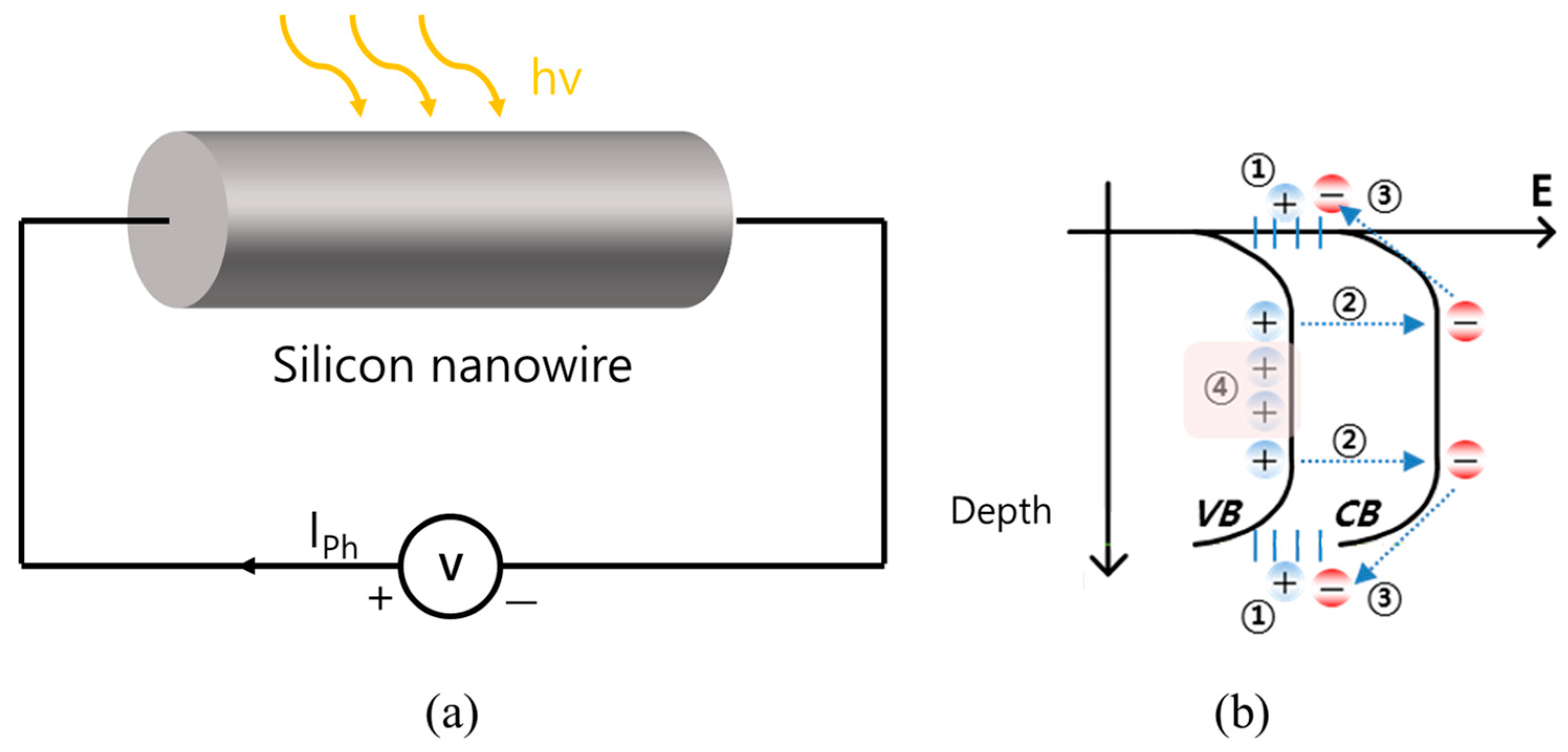
2.1. Theoretical Consideration: Photoresponsivity of SiNW Photodetector

The principle of solid-state optoelectronic devices basically relies on the Beer–Lambert law, which is shown in Equation (1):
P = 1 e α x
where P is a percentage of the light absorbed, α is an absorption coefficient, and x is the path length of the light. According to this equation, most energy of incident light illuminating the bulk semiconductor is absorbed at the surface. When a uniform optical injection occurs on the p-type semiconductor, the conductivity at the surface increases as follows:
σ = σ 0 + Δ σ = q μ n n 0 + μ p p 0 + q μ n Δ n + μ p Δ p
where σ0 is dark conductivity, Δσ is the difference between conductivity in the dark state and under illumination, q is the electron charge, µ is the carrier mobility, n0 and p0 are electron and hole concentrations in the dark state, and Δn and Δp are excess carrier concentrations. Therefore, the photocurrent is defined as the following equation:
I p h = q A Δ n v d = q A Δ n L t n = q A L g τ n t n τ n t n
Figure 2a illustrates a simplified model of the SiNW photodetector discussed in this paper to explain the operation. SiNW photodetectors have high photoconversion gain due to structural characteristics [19]. Surface states increase carrier recombination rates and affect devices with high surface-to-volume ratios like nanowires. When the device is in a dark environment and no light is absorbed by the nanowire, mobile carriers are trapped on the surface. The inside of the nanowire is, therefore, fully depleted. As shown in Figure 2b, when the nanowire is illuminated, electron-hole pairs are generated. The photons with energy greater than the bandgap of the silicon excite the carriers and create electrons in the conduction band. The remaining holes stay at the core of the nanowire, which contributes to photocurrent when the device is biased. Therefore, the lifetime and the transit time of the holes (majority carriers) contribute to the photocurrent, whereas minority carriers play dominantly in conventional photodetectors. Hence, similarly to Equation (3), the internal conductive gain of the SiNW (GNW) can be expressed as a ratio of the hole lifetime (τp) (GNW = τp/tp) as derived in the previous research [26].
The photoconductive gain of the conventional bulk Si photoconductor depends on the recombination rate of minority carriers, “τn/tn”. On the contrary, the gain of the SiNW can be expressed as the function of majority carriers, “τp/tp”. The typical recombination rate, “τn”, for the photodetector is several nanoseconds, and the hole lifetime, “τlp”, of the SiNW is several microseconds. Therefore, assuming the transit time is the same, the SiNW has a much greater gain than that of conventional photodetectors.

2.2. Fabrication of Vertically Stacked SiNW Photodetector

Figure 3 illustrates the fabrication process of the top-down SiNW photodetector. The photodetector is fabricated on a p-type (100) silicon-on-insulator (SOI) wafer with a diameter of 100 mm, a 2 μm-thick buried oxide (BOX) layer, and a 400 μm-thick Si handle layer. The SOI wafers containing top silicon device layers with thicknesses of 1 μm, 3 μm, and 5 μm were used to create photodetectors with varying numbers of SiNW layers. This is because the potential number of SiNW layers is determined by the thickness of the silicon device layer on the SOI. Firstly, the electrode area on the SOI device layer, excluding an area of 200 μm by 200 μm, is patterned using AZ4330 photoresist (PR). Metal electrodes, i.e., titanium (Ti) with a thickness of 400 Å and aluminum (Al) with a thickness of 2000 Å, are deposited onto the open area, with the Ti layer deposited beneath the Al layer for improved adhesion with the Si device layer. Subsequently, the electrode layer of the photodetector is fabricated through a lift-off process. To form the SiNW array on the silicon device layer with the electrodes, the SS03A9 PR is spin-coated at 4500 RPM. The coated PR is then exposed to a wavelength of 405 nm (H line). The pattern width of the SiNW is 0.5 μm, the pitch is 1 μm, and the length is 10 μm.
The nanowires are fabricated using the modified deep-reactive-ion etching (DRIE) method proposed in our previous work [27]. The DRIE process involves repeated cycles of isotropic silicon etching and passivation layer deposition, which enables the implementation of structures with a high-aspect ratio. Since the SiNW pattern width is 0.5 μm, the target for scallop dimension during isotropic silicon etching is set to 0.25 μm. Consequently, scallops are formed simultaneously on both sides of the pattern during the isotropic etching, enabling the stacking of horizontal nanowires. The SiNW array can be stacked to increase its density by adjusting the number of cycles of the DRIE process. The proposed fabrication method enables an increase in the SiNW density within a finite dimension. Following the formation of the SiNW, the PR on the surface is removed through O2 plasma ashing. Rapid thermal annealing (RTA) is then performed to reduce the contact resistance between the metal electrodes and the Si layer, thereby maximizing the gating effect induced by the photons.

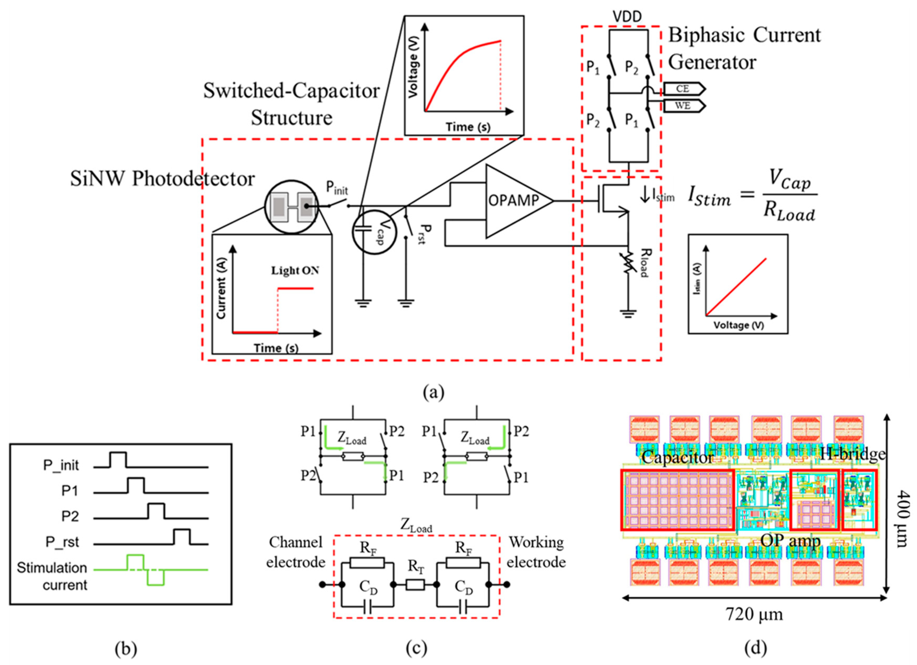
2.3. Switched Capacitor Biphasic Current Stimulator

Figure 4a illustrates a detailed schematic diagram of the developed biphasic current stimulator circuit, which is integrated with the SiNW photodetector. The current generated by the SiNW is converted into voltage using a switched-capacitor structure, ensuring a stable voltage supply. Subsequently, a rail-to-rail folded cascode amplifier is designed to utilize the entire voltage input range from 0 to Vdd. The output stage of the amplifier, which is designed as a single-end output, is connected to the NMOS, which regulates the current flowing through the working electrode (WE) and counter electrode (CE) in the biphasic current stimulator. The stimulation current can also be controlled by adjusting the load resistor (Rload) connected to the H-bridge. The SiNW photodetector array and stimulator circuit operate at a relatively low supply voltage of 3V.
The stimulator-integrated circuit (IC) operation employs four control signals. Figure 4b presents a timing diagram of the control signal and the generated stimulation current. The stimulator circuit begins operation upon receiving the Pinit signal and concludes by discharging and resetting the accumulated charge via the Prst signal. The Pinit signal charges the capacitor with the current flowing through the SiNW photodetector and converts it into voltage. The voltage across the capacitor is proportional to the integral of the current in the photoresistor over time. Consequently, the gain and amplitude of the stimulation current can be effectively regulated by adjusting the duration of the Pinit signal, which determines the charging time of the capacitor.
The biphasic current pulse generator comprises switches, P1 and P2. Figure 4c depicts each state of the biphasic current pulse flow. The stimulator is designed to control the injected current to 200 μA, with two switches operating complementarily. When P1 is ON and P2 is OFF, the current flows from the working electrode (WE) to the counter electrode (CE) through Zload. Subsequently, P1 is turned off and P2 is turned on simultaneously for charge balance, since the same amount of injected charge must be removed to prevent electrode corrosion. In retinal stimulation, the stimulation IC interfaces with the retinal tissues via an MEA, utilizing a parallel configuration of a resistor (R) and capacitor (C) [28,29]. As shown in Figure 4c, the Zload is composed of faradic charge transfer resistance, tissue layer impedance, and double-layer capacitance. The values utilized in this paper are derived from data obtained in a previous study [30] and have been employed to design the circuit accordingly. The Faradic charge transfer resistance (RF) is 13.18 MΩ, and tissue impedance (RT) is 250.62 Ω. The double-layer capacitance (CD) is 124.58 nF. Figure 4d depicts the top layout of the stimulator circuit. The stimulator is fabricated using the CMOS 180 nm TSMC technology, and the dimension of a pixel is 740 μm × 400 μm.
The optical and electrical characteristics of the SiNW photodetectors are measured using a semiconductor parameter analyzer (4200A-SCS; Keithley, Cleveland, OH, USA). The measurements are conducted in a probe station inside a dark box, where the probes are connected to the electrodes, as shown in Figure 5a. A halogen light source is used for illumination, and the light intensities are measured using a digital lux meter (MEXTECH, LX-1010B; Mextech, Mumbai, India). Furthermore, the photodetector is exposed to light with wavelengths ranging from 400 nm to 800 nm to analyze the wavelength-dependent photoresponsivity. Light with different wavelengths is directed onto the photodetector using a monochromator, and the power density is measured using an optical power meter (Thorlabs PM100USB; Thorlabs Inc., Newton, NJ, USA), as shown in Figure 5b. An FPGA test board is prepared to transmit digital control signals to control the Pinit, Prst, P1, and P2 timing signals. As shown in Figure 5c, the SiNW photodetector and developed stimulator IC are integrated with the FPGA board.

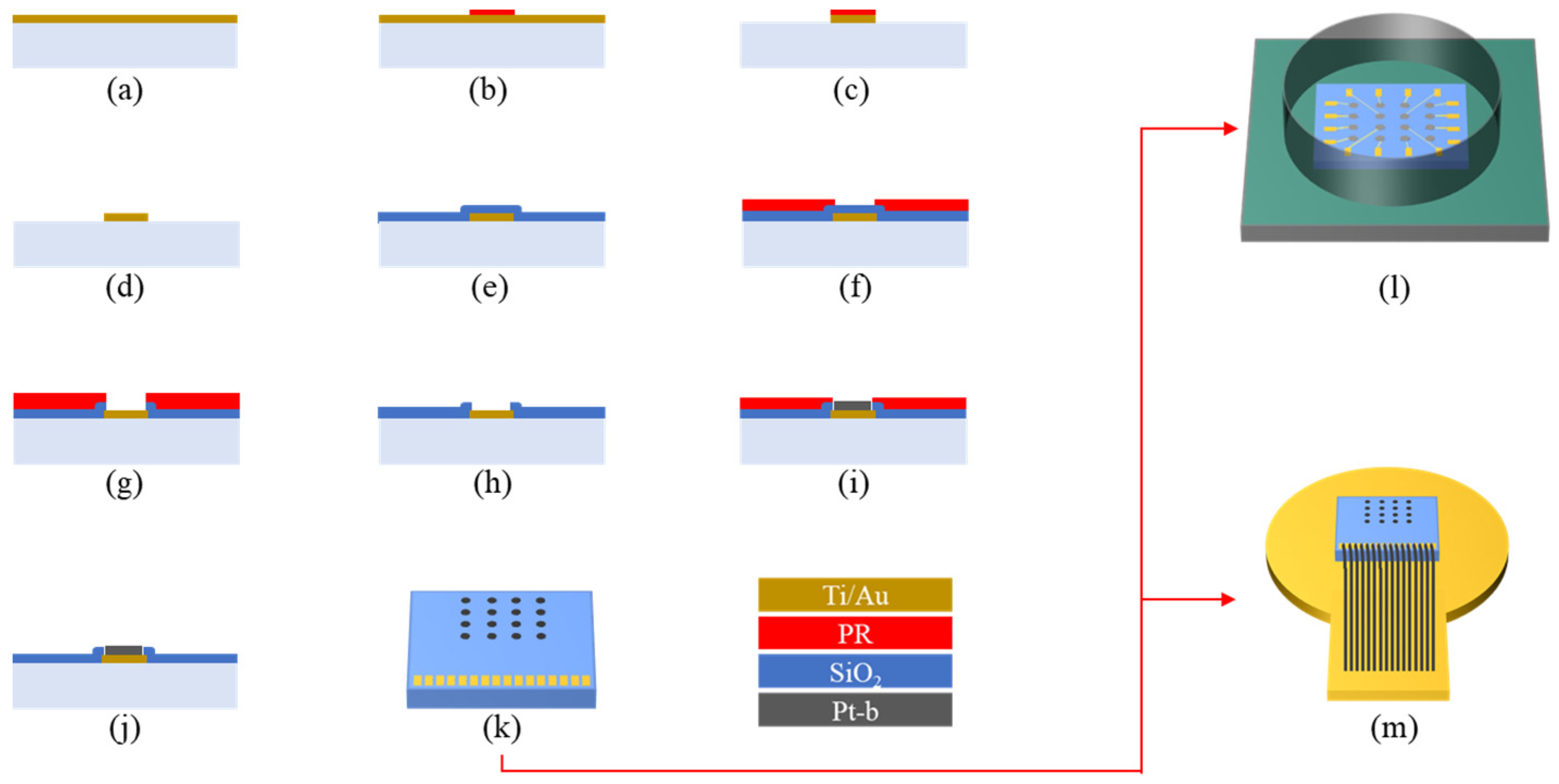
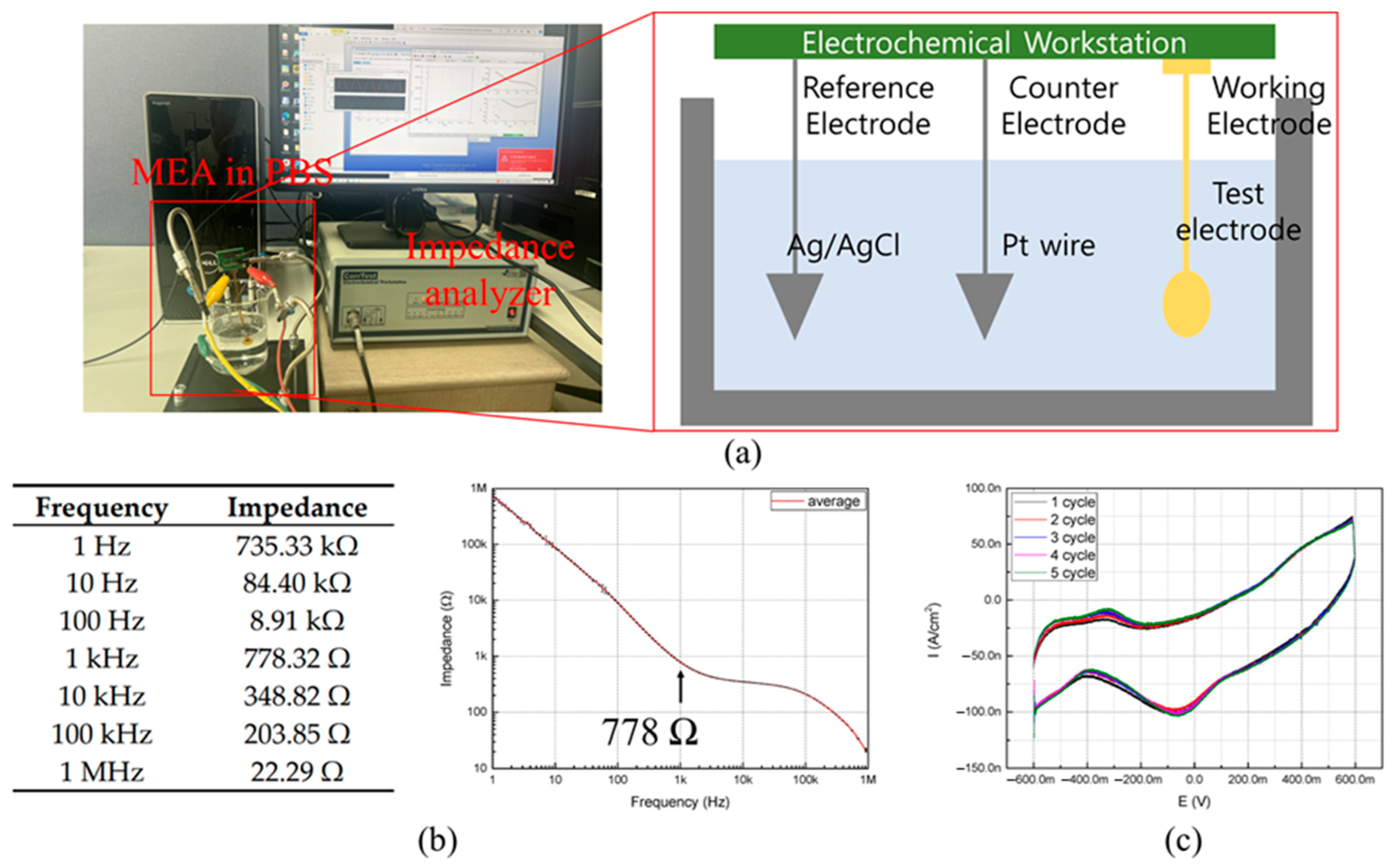
2.4. Fabrication of Nanostructured Platinum-Black MEA

In retinal stimulation, a crucial objective is to decrease interface impedance while maintaining a small base area. In this paper, electrodes plated with platinum black (Pt-black) are fabricated to achieve low contact impedance with the retinal cells and to allow high current injection [30]. The Pt-black layer features a wide surface area due to its nano-porous structure, which effectively lowers the interface impedance between the microelectrodes and the retinal cells and increases the charge injection capacity. The fabrication process is illustrated in Figure 6. In this paper, the glass MEAs with an electrode size of 50 µm are connected to a printed circuit board (PCB) using a wire bonding process for subsequent in vitro experiments.
The fabrication process of the implantable nanostructured MEA begins with a Pyrex 7740 borosilicate glass wafer, used as a substrate. The initial step involves sputtering 300 Å of Ti for adhesion and 500 Å of gold (Au) for the metal interconnection layer. These layers are then patterned using photolithography and chemical etching processes. The isolation layer is created through sequential chemical vapor deposition (CVD) of tetraethylorthosilicate (TEOS), photolithography, oxide etching, and ashing. Subsequently, a second layer of Ti/Au is sputtered to serve as a seed layer for the electroplating of nanostructured Pt-black on the stimulation electrodes and interconnection pads. Oxygen plasma treatment is used to enhance the adhesion before the electroplating of a 3 µm thick Au layer and the Pt-black layer. Afterward, the Au seed layer is removed, and the glass wafer is thinned to 100 µm by backside grinding.
The type of substrate used for mounting MEAs determines whether the setup is suitable for in vitro or in vivo experiments. In the fabrication process for in vitro experiments, as shown in Figure 6l, the glass MEAs are attached to a printed circuit board (PCB) through a wire bonding process. For in vivo applications, detailed in Figure 6m, the MEA body and cover layers are fabricated using polyimide, a polymer known for its flexibility and resistance to heat and chemicals. The polyimide serves as a robust body for the implantable electrodes. In this process, laser cutting technology is used to create the polyimide body and cover, after which the diced glass MEA is wire-bonded to the polyimide layer, preparing it for implantation.

3. Results

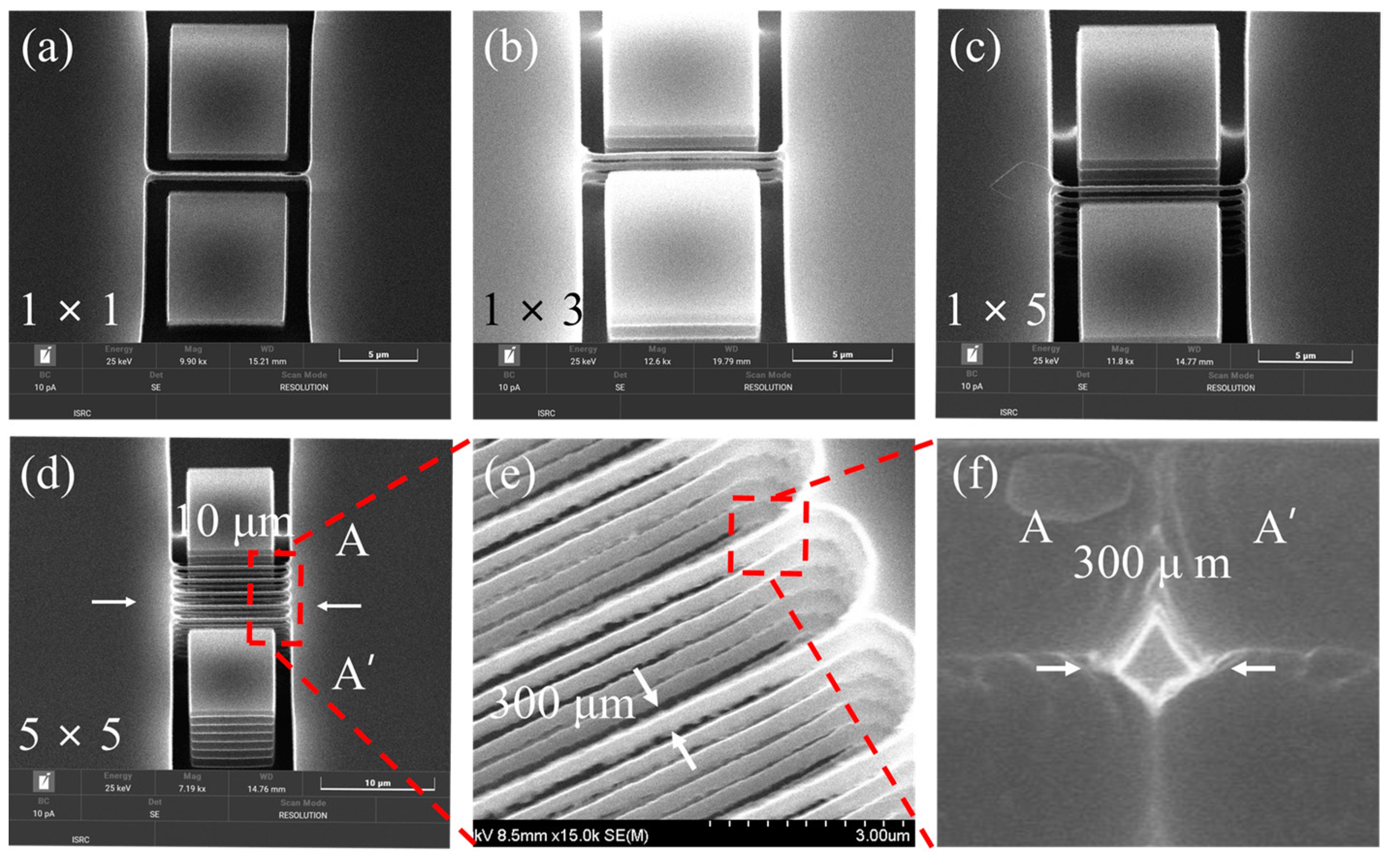
3.1. Fabrication Results of Vertically Stacked SiNW Photodetector

Figure 7a–c depict the fabricated SiNW arrays with configurations of 1 × 1, 1 × 3, and 1 × 5 using a modified DRIE process. A single SiNW was fabricated in multiple vertical layers, thereby increasing the density of the SiNWs within a finite-dimensional space. The scanning electron microscopy (SEM) analysis confirmed the precise fabrication of the various three-dimensional SiNW arrays. To evaluate the uniform fabrication of various SiNW array structures, 5 × 5 SiNW arrays were also fabricated. The overall dimensions and structure were analyzed using SEM.
Figure 7d,e present the tilted views of the light-sensing part of the photodetector. A uniformly suspended 5 × 5 SiNWs array, with a thickness of 300 nm and a length of 10 μm, was observed. Figure 7f depicts the specific dimensions and cross-sectional view of the SiNWs. The diameter of the SiNWs was approximately 300 nm, and they exhibited a rhombus shape owing to the modified DRIE process. By tuning the width of the PR pattern and adjusting etch parameters, the dimensions of the SiNWs could be controlled, yielding various diameters.

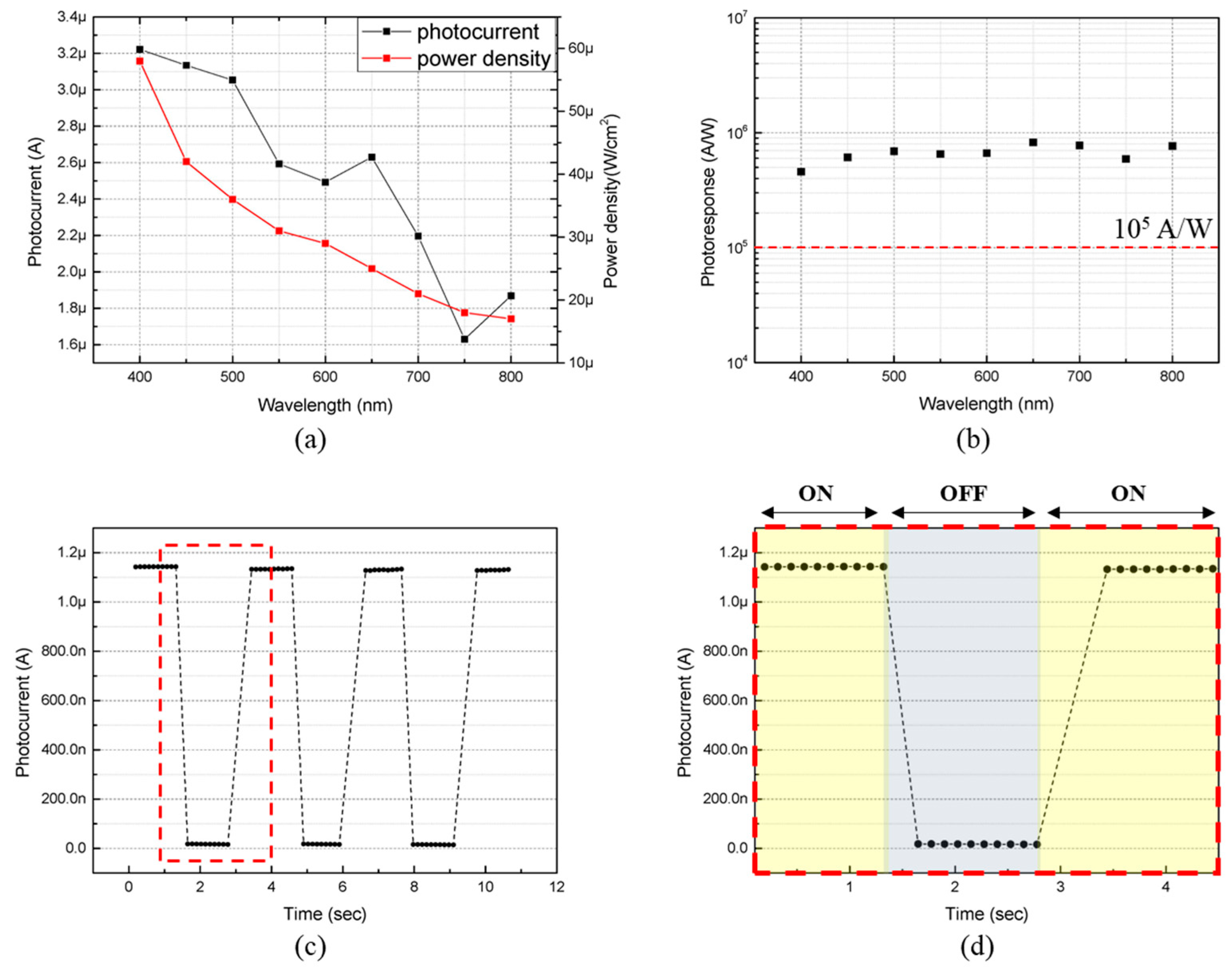
3.2. Electrical and Optical Characteristics of SiNW Photodetector

Figure 8a shows the I–V characteristics of the 1 × 5 SiNW photodetector in both the dark and illuminated states with a light intensity of 1.5 mW/cm2 across a voltage range from 0 V to 1 V. The measurements obtained from each of the eight devices reveal linear characteristics under both conditions, confirming the establishment of an ohmic contact between the metal electrodes and the silicon device layer. Additionally, an increase in the light intensity leads to an increase in the photocurrent, which has the effect of decreasing the resistance of the SiNWs. In the dark state, holes are trapped at the surface of the nanowires, leading to complete depletion inside the photodetector and resulting in high resistance values, typically within the range of several mega-ohms. However, electron-hole pairs are generated when external light illuminates the nanowires, causing photoexcited electrons to populate the conduction band [31]. These excited electrons and trapped holes recombine at the surface, leaving holes in the core of the nanowire, which contributes to the generated current.
Figure 8b illustrates the photocurrent responses of the three photodetectors, each comprising a SiNW structured into 1 × 1, 1 × 3, and 1 × 5 arrays under varying light intensities. The three devices were subjected to broad-spectrum white light illumination, ranging from 0 mW/cm2 (dark state) to 1.6 mW/cm2 (10,000 lux) under a bias voltage of 3 V. Each device generated a greater photocurrent with the increase in the intensity of the illuminated light, which was distinguishable across a broad spectrum of light intensities. The devices exhibit higher photosensitivity with the increase in the density of the SiNWs owing to the enhanced surface-to-volume ratio. At 5000 lux, the photocurrents for the devices were measured at 5.5 µA, 2.4 µA, and 0.8 µA, respectively. The near-linear increase in photocurrent with additional layers indicates that the effect of the upper layers on the lower layers is negligible during the photoreaction. All three devices exhibited high photosensitivity at low light intensities, and the rate of increase diminished with the increase in the light intensity. When SiNWs are illuminated, the electrons generated by the electron-hole pairs recombine with the surface carrier traps, while the photogenerated holes remain in the nanowires, contributing to an increase in the output current. At low illuminance, a gradual increase in the light intensity generates more electron-hole pairs, leading to a rapid increase in the photocurrent. However, at higher light intensities, the reduction in the density of the available carrier traps within the nanowire causes a photo-response saturation [32]. Thus, the SiNWs demonstrate high photosensitivity under low-light conditions, which can be advantageous in indoor lighting environments.
Figure 9a presents the results of an experiment evaluating the wavelength dependency of the photoresponsivity. The 1 × 5 SiNW photodetector was illuminated with light of wavelengths ranging from 400 nm to 800 nm using a monochromator at a bias voltage of 3 V. A distinguishable photocurrent was measured at each wavelength. The power density peaked at 1.18 mW/cm2 within the 400 nm wavelength range and decreased to 0.37 mW/cm2 at the 800 nm wavelength range. The power density typically decreases with the increase in the wavelength, leading to a corresponding decrease in the photocurrent response. The photoresponsivity at each wavelength was calculated as follows:
P h o t o r e s p o n s i v i t y = P h o t o c u r r e n t D a r k   c u r r e n t   P o w e r   d e n s i t y × E f f e c t i v e   a r e a A / W
A photoresponsivity of over 105 A/W was measured across all the wavelength ranges with an increase in wavelength, as shown in Figure 9b. The effective area of the device is approximately 1 µm × 10 µm, which is small enough to contribute to the superior photoresponsivity of the SiNWs. Figure 9c shows that the photo-switching response of the 1 × 5 SiNW photodetector was stable and repeatable when the light illumination cycles between the ON (100 lux) and OFF states at a bias voltage of 1 V. This result indicates the reliable performance of the device under repeated light exposure. Figure 9d details the response dynamics of the photodetector, with the falling time recorded at 0.32 s and the rising time at 0.76 s.

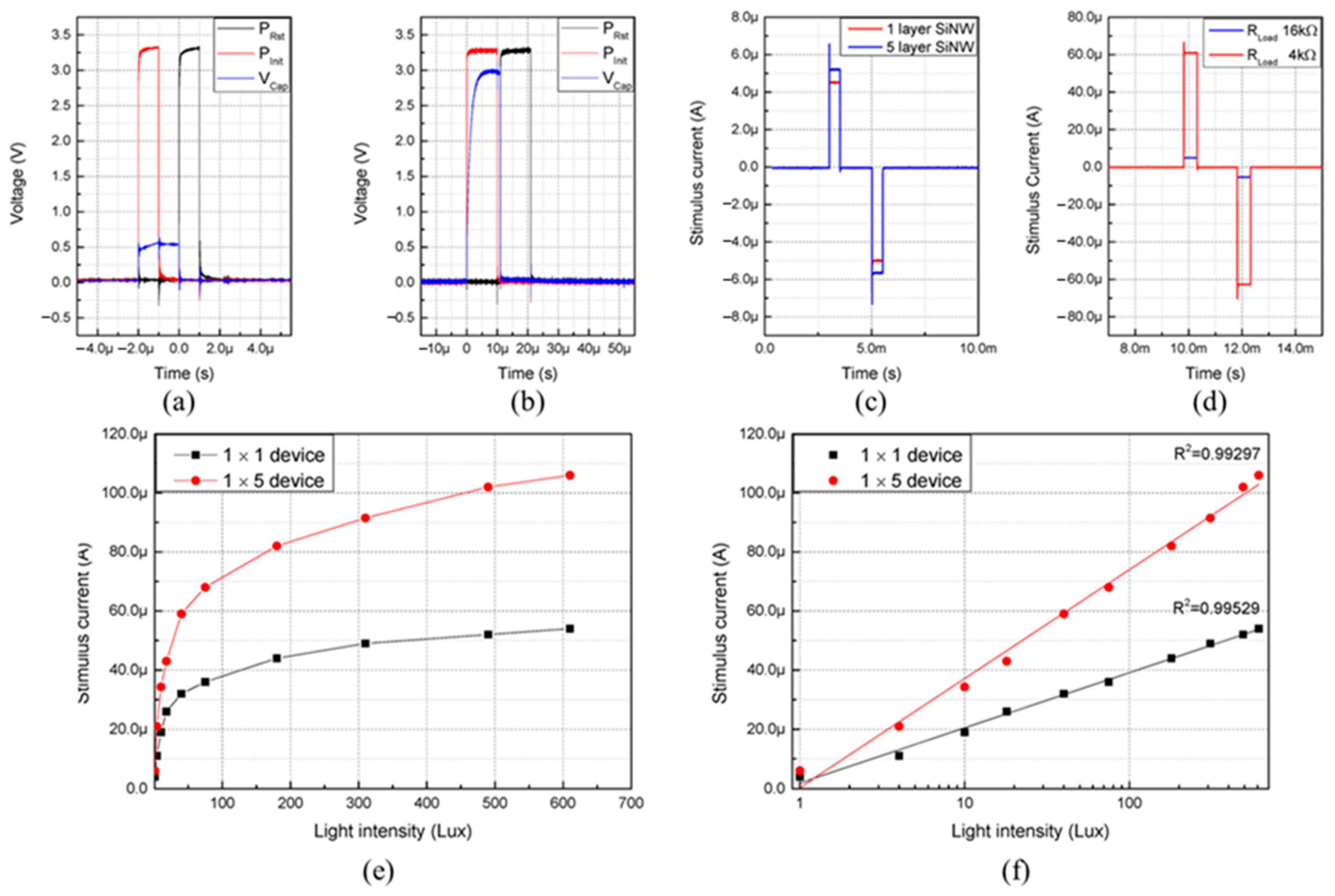
3.3. Evaluation of SiNW Photodetector-Integrated Stimulator Circuit

Figure 10a presents a die photograph of the fabricated stimulator IC, and Figure 10b presents a simplified schematic diagram of the switched capacitor structure. The capacitor was charged using a DC power supply through a SiNW photodetector. The duration of the Pinit signal affects the charging period of the capacitor and the gain of the stimulation current.
Figure 11a,b depict the relationship between the duration of the Pinit signal and the voltage across the charging capacitor under a bias voltage of 3 V. When a constant light intensity of 5000 lux illuminated the 1 × 5 array SiNW photodetector, an initializing pulse of 1 μs charged the capacitor to approximately 0.56 V, while extending the pulse duration to 10 μs increased the charged voltage to approximately 2.98 V. Figure 11c illustrates the generation of the biphasic pulses with different numbers of SiNW layers at a bias voltage of 3 V. As the light intensity increased to 100 lux, the stimulation current amplitude was observed to be very sensitive to the light intensity, reaching approximately 4.2 µA in a 1 × 1 device and 5.1 µA in a 1 × 5 device. Additionally, under the same bias voltage of 3 V, the stimulation current could be controlled by adjusting the load resistor connected to the H-bridge. At a constant light intensity of 100 lux and a charge duration of 0.5 ms, changing the load resistor values from 4 kΩ to 16 kΩ affected the amplitude of the biphasic pulse. When the resistance was reduced from 16 kΩ to 4 kΩ, the stimulus current was observed to increase from 5.7 µA to 62 µA, as shown in Figure 11d. Prior to the in vitro experiment, stimulus currents were measured over a charging time of 0.5 ms in response to varying light intensities, ranging from 1 lux to 610 lux. The experiment was repeated to compare the amplitudes of the stimulus currents of the 1 × 1 and 1 × 5 devices. In Figure 11e, the amplitudes of the stimulus currents are plotted as functions of the light intensity. Specifically, the measured stimulus current was observed to be 12 μA when utilizing a 1 × 5 array SiNW photodetector under the illumination of 4 lux. With a pulse duration of 50 μs and at this stimulus current level, an injection of 1.2 nC per pulse is feasible, which substantially exceeds the threshold required for inducing a neural response [33]. The amplitudes of the stimulus currents are proportional to the incident light power on a logarithmic scale, as shown in Figure 11f. The sensitivity of the SiNW remained high, despite the low light intensities that were observed.

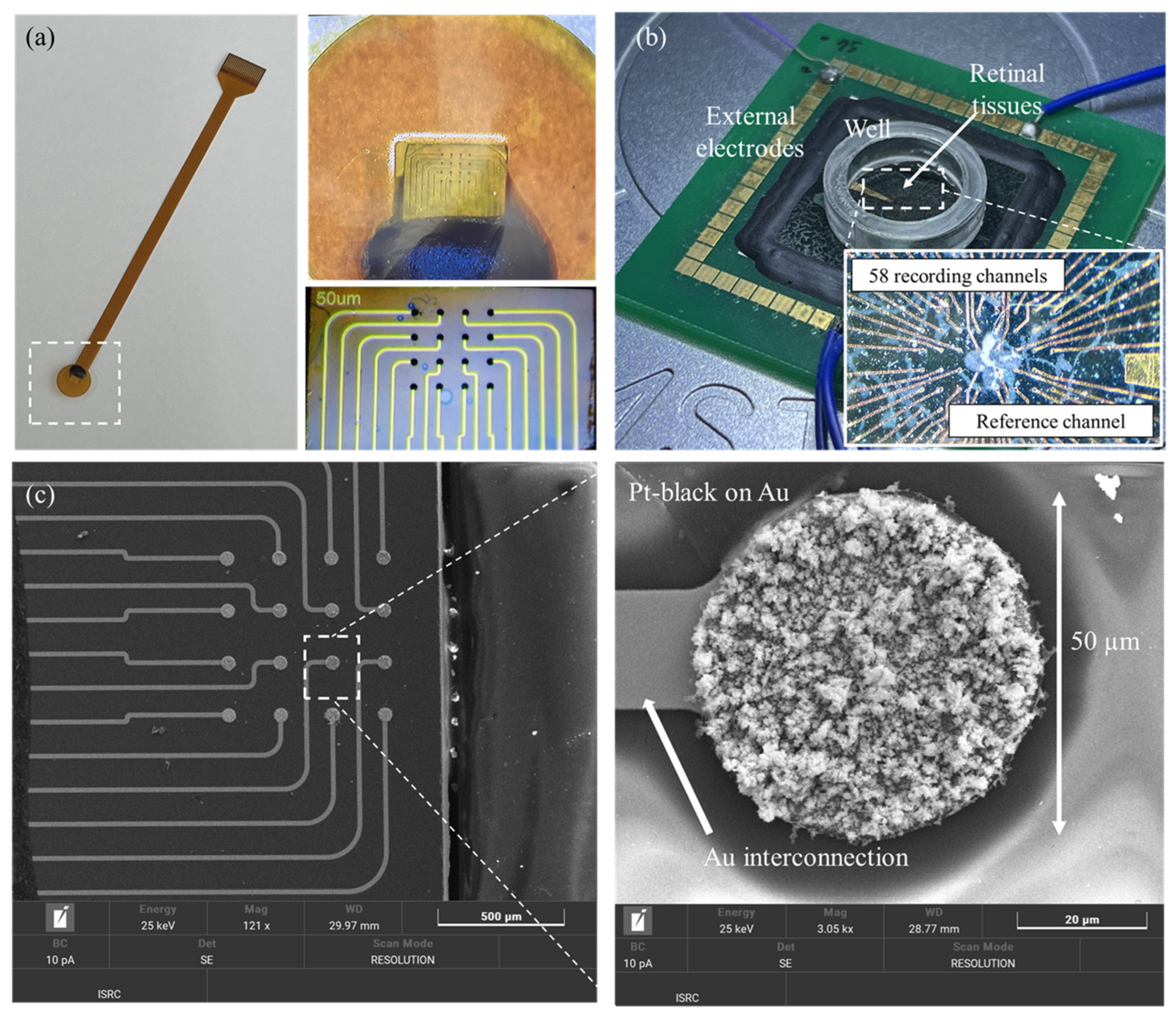
3.4. Fabrication Results of Pt-Black MEA

Figure 12 shows the fabrication results of the nanostructured MEAs designed for both in vivo and in vitro experimental applications. Figure 12a shows the fabrication results of the nanostructured microelectrodes on a polyimide layer, suitable for in vivo experiments. The final device was assembled through a wire-bonding process with 16 microelectrodes in a 4 × 4 grid. Figure 12b demonstrates the device designed for in vitro experiments, fabricated on a PCB. This setup included an MEA with an inner well for cell manipulation and outer electrodes that connect to the MEA-60 recording system (Multi Channel Systems GmbH, Kusterdingen, Germany). The glass MEA comprised 61 microelectrodes, including 1 reference electrode, 58 recording electrodes, and 2 stimulation electrodes. The stimulator charge was injected through the stimulation electrodes, while the remaining 58 electrodes were used to record the neural response signals. The glass MEAs were attached to the PCB via a wire-bonding process. The PCB measured 49 mm × 49 mm, with typically 60 microelectrodes arranged in an 8 × 8 grid and an interelectrode distance of 200 µm. The SEM images of the fabricated MEAs are shown in Figure 12c. The nanostructures of the electroplated Pt-black were well attached to the Au layer. Each microelectrode, which comprised a circular electrode with a diameter of 50 µm, was fabricated by depositing an Au layer followed by a Pt-black layer. From the surface SEM image, the Pt structures exhibited a highly porous morphology, resulting in a significantly large surface area.
Figure 13a shows the experimental setup to measure the electrode–electrolyte interface impedance and perform cyclic voltammetry (CV) to analyze the nanostructured Pt-black microelectrodes using a three-element circuit model. An impedance analyzer, CS350 (Wuhan CorrTest Instruments Co. Ltd., Wuhan, China), was used for these measurements. The MEAs were dipped in a phosphate-buffered saline (PBS) solution, and impedance measurements were taken at frequencies ranging from 1 Hz to 1 MHz.
Figure 13b summarizes the average impedance measurements at different frequencies for five distinct electrodes with a diameter of 50 µm. The measured impedance at a frequency of 1 kHz was approximately 779 Ω. As the frequency increased, the measurements remained below 1 kΩ above 1 kHz. This ensures that large currents can be driven to retinal cells despite the small surface area, which is essential for effective cell current driving. The CV measurements were conducted with a voltage sweep from −0.6 V to 0.6 V at a slew rate of 50 mV/s for 5 cycles. The charge storage capacities (CSCs) of the nanostructured Pt-black MEAs were calculated from the CV curves shown in Figure 13c by integrating the current over the full potential cycle within the sweep range. The measured results indicate CSCs of 0.778 mC/cm2.

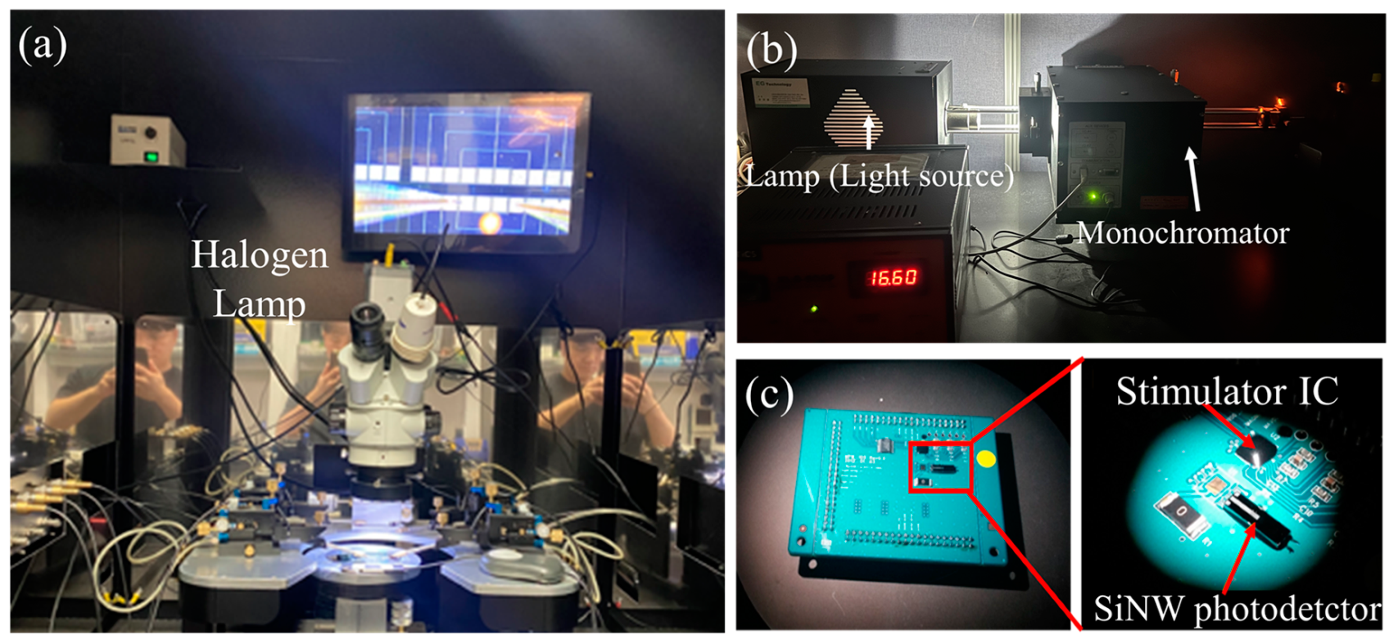
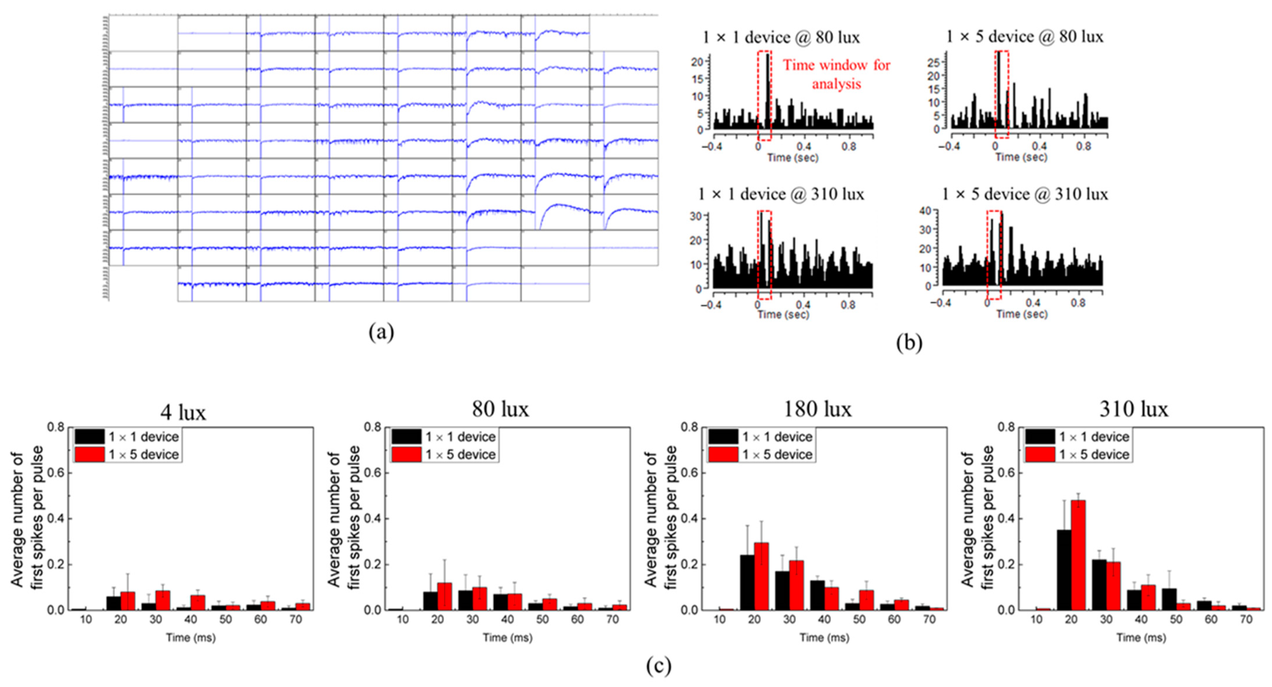
3.5. In Vitro Experiment

In vitro experiments were conducted to evaluate the photoresponsivity of vertically stacked nanowires. The purpose was to observe cellular responses to higher stimulation currents as the density of vertically stacked SiNWs increases under constant light intensity. The study focused on identifying differences rather than performing a quantitative analysis. Figure 14a depicts the experimental configuration. The setup included a multilayer SiNW photodetector, a stimulator IC, an FPGA test board, and a halogen lamp. The stimulator circuit, integrated with either a 1 × 1 or 1 × 5 array SiNW photodetector, was tested repeatedly across a range of light intensities increasing from 4 lux to 310 lux. The capacitor charging time was 0.5 ms, and the load resistor value was set to 4 kΩ.
For the in vitro experiments, degenerated retinal tissue was extracted from the eyes of rd1 mice. It was then cut into 5 mm × 5 mm retinal patches for use in the experiment. From the retinal patch, three cells showing the strongest and most consistent responses to electrical stimulation were selected for data analysis. As shown in Figure 14b, this retinal patch was mounted on Pt-black electrodes and used for the experiment. Surrounding the retinal patch, a well-structured cavity was formed, which was subsequently filled with cerebrospinal fluid (CSF). This setup enabled the retinal cell to maintain its functionality over an extended period.
The stimulator IC injected a stimulation current into the RGCs every 1 s for 1 min at fixed light intensities, and the experiment was repeated with the 1 × 1 and 1 × 5 array SiNW photodetectors. The SALPA algorithm was used to reduce the overall noise level of recorded responses, suppressing various types of background noise that might interfere with spike detection. After noise reduction, the first spike was detected using the method reported in a previous study [34]. Figure 15a shows the neural response signals when the stimulation signal was applied. The effectiveness of the stimulation was assessed by observing significant changes in the number of spikes following the application of the stimulation signal. Figure 15b illustrates the post-stimulus time histogram (PSTH) of the neural signals recorded from each electrode that exhibited a strong response to stimulation in the in vitro experiment. The PSTH demonstrates that most neural spikes were evoked by current stimulation resulting from an increase in light intensity in the same SiNW photodetector, indicating high sensitivity to low light levels. Furthermore, at the same light intensity, the number of neural spikes increased with the SiNW density, revealing enhanced light sensitivity due to the higher density of SiNWs.
The number of spikes after stimulation was subtracted from the number of spikes before stimulation. The average number of neural spikes per stimulation was then calculated by dividing this difference by the total number of stimulations. Cells with a spike count difference of 0 or less were excluded from the analysis, as these cells likely had poor electrode contact, resulting in improper response recording. After excluding these cases, the three cells with the strongest responses were selected for further analysis. Figure 15c depicts the average number of first spikes per pulse during the medium latency period (3–70 ms) for the 1 × 1 and 1 × 5 array SiNW photodetectors at light intensities of 4, 80, 180, and 310 lux. The average number of electrically evoked neural spikes was calculated from the PSTH of electrodes that strongly responded to the stimulation. Shorter latencies of the first spikes were observed with increases in both the SiNW density and light intensity, as shown in Figure 15. As the density of the SiNW arrays increased from 1 × 1 to 1 × 5, the number of neural responses increased in each light intensity condition. Additionally, the experimental results demonstrate that the stimulator IC achieves high photosensitivity at low light intensities.

4. Discussion and Conclusions

In this study, a vertical high-density SiNW photodetector was fabricated and integrated into a switched capacitor stimulator circuit for retinal prosthesis applications. SiNW arrays with a diameter of 300 nm were fabricated in multiple layers using a simplified and modified DRIE process. This fabrication process enabled the creation of high-density SiNW configurations with finite dimensions. The electrical and optical characteristics of the SiNW photodetector were measured to assess its feasibility for retinal prosthesis applications. The linear I–V characteristics confirmed the formation of an ohmic contact between the Ti/Al electrodes and the silicon device layer. The optical properties demonstrated that higher current amplitudes can be generated under the same illumination conditions as the vertical density of the SiNW layers increased, owing to the increased light absorption and enhanced photoelectric response. The SiNW photodetector developed in this study achieves superior photoresponsivity and sensitivity in a smaller area due to its vertically stacked structure. This makes it advantageous for miniaturized applications such as retinal implants. The lower dark current of 56 nA, compared to 100–178 nA in previous studies [35], provides higher sensitivity under the same photocurrent conditions. The fabricated device operated effectively under various lighting conditions and was particularly sensitive to low light intensity. Moreover, it exhibited excellent photoresponsivity, exceeding 105 A/W across the wavelength range of 400–800 nm. The SiNW photodetectors were integrated with a switched capacitor stimulator circuit, demonstrating that the stimulation current increased proportionally with the light intensity and SiNW density. The stimulus currents were effectively controlled by adjusting the charging time and load resistance. The in vitro experiments, which were measured electrically, evoked neural responses from retinal cells, indicating that more neural spikes were evoked as the light intensity and SiNW density increased. Notably, these findings demonstrate that high photosensitivity was ensured even at low light intensities, with its benefits becoming especially evident under typical indoor conditions. This study provides guidelines for the integration of SiNW photodetector systems, serving as a test bench that can contribute to the advancement of direct implantable integrated retinal prosthesis systems. The integration of vertical high-density vertically stacked SiNW photodetectors with a switched capacitor stimulator circuit presents considerable potential in high-resolution retinal prosthesis applications.

Author Contributions

S.L. supervised the study; T.K. and S.H. designed and fabricated the device; T.K. and S.H. conducted the experiments; S.L., T.K. and S.H. wrote the paper. All authors have read and agreed to the published version of the manuscript.

Funding

This research was supported by the MSIT (Ministry of Science and ICT), Korea, under the ITRC (Information Technology Research Center) support program (IITP-2024-RS-2024-00438239), supervised by the IITP (Institute for Information and Communications Technology Planning and Evaluation).

Institutional Review Board Statement

Not applicable.

Informed Consent Statement

Not applicable.

Data Availability Statement

The data are contained within the article.

Conflicts of Interest

The authors declare no conflicts of interest.

References

  1. Hartong, D.T.; Berson, E.L.; Dryja, T.P. Retinitis Pigmentosa. Lancet 2006, 368, 1795–1809. [Google Scholar] [CrossRef] [PubMed]
  2. Deng, Y.; Qiao, L.; Du, M.; Qu, C.; Wan, L.; Li, J.; Huang, L. Age-Related Macular Degeneration: Epidemiology, Genetics, Pathophysiology, Diagnosis, and Targeted Therapy. Genes Dis. 2022, 9, 62–79. [Google Scholar] [CrossRef]
  3. Congdon, N.; O’Colmain, B.; Klaver, C.C.W.; Klein, R.; Muñoz, B.; Friedman, D.S.; Kempen, J.; Taylor, H.R.; Mitchell, P. Causes and prevalence of visual impairment among adults in the Unites States. Arch. Ophthalmol. 2004, 122, 477–485. [Google Scholar]
  4. Jones, B.W.; Marc, R.E. Retinal Remodeling during Retinal Degeneration. Exp. Eye Res. 2005, 81, 123–137. [Google Scholar] [CrossRef] [PubMed]
  5. Marc, R.E.; Jones, B.W.; Watt, C.B.; Strettoi, E. Neural Remodeling in Retinal Degeneration. Prog. Retin. Eye Res. 2003, 22, 607–655. [Google Scholar] [CrossRef]
  6. Luo, Y.H.L.; da Cruz, L. The Argus® II Retinal Prosthesis System. Prog. Retin. Eye Res. 2016, 50, 89–107. [Google Scholar] [CrossRef] [PubMed]
  7. Scribner, D.; Johnson, L.; Klein, R.; Bassett, W.; Howard, J.; Skeath, P.; Wassetman Humayun, L.B.; Perkins, F.; Peckerar, M.; Finch, B.J.; et al. A Retinal Prosthesis Device Based on an 80 × 40 Hybrid Microelectronic-Microwire Glass Array. In Proceedings of the IEEE 2003 Custom Integrated Circuits Conference, San Jose, CA, USA, 24 September 2003. [Google Scholar]
  8. Stingl, K.; Schippert, R.; Bartz-Schmidt, K.U.; Besch, D.; Cottriall, C.L.; Edwards, T.L.; Gekeler, F.; Greppmaier, U.; Kiel, K.; Koitschev, A.; et al. Interim Results of a Multicenter Trial with the New Electronic Subretinal Implant Alpha AMS in 15 Patients Blind from Inherited Retinal Degenerations. Front. Neurosci. 2017, 11, 445. [Google Scholar] [CrossRef]
  9. Wu, C.Y.; Tseng, C.K.; Liao, J.H.; Chiao, C.C.; Chu, F.L.; Tsai, Y.C.; Ohta, J.; Noda, T. CMOS 256-Pixel/480-Pixel Photovoltaic-Powered Subretinal Prosthetic Chips with Wide Image Dynamic Range and Bi/Four-Directional Sharing Electrodes and Their Ex Vivo Experimental Validations with Mice. IEEE Trans. Circuits Syst. I Regul. Pap. 2020, 67, 3273–3283. [Google Scholar] [CrossRef]
  10. Tomioka, K.; Toyoda, K.; Ishizaki, T.; Noda, T.; Ohta, J.; Kimura, M. Retinal Prosthesis Using Thin-Film Devices on a Transparent Substrate and Wireless Power Transfer. IEEE Trans. Electron Devices 2020, 67, 529–534. [Google Scholar] [CrossRef]
  11. Park, J.H.; Tan, J.S.Y.; Wu, H.; Dong, Y.; Yoo, J. 1225-Channel Neuromorphic Retinal-Prosthesis SoC with Localized Temperature-Regulation. IEEE Trans. Biomed. Circuits Syst. 2020, 14, 1230–1240. [Google Scholar] [CrossRef]
  12. Muqit, M.M.K.; Hubschman, J.P.; Picaud, S.; McCreery, D.B.; Van Meurs, J.C.; Hornig, R.; Buc, G.; Deterre, M.; Nouvel-Jaillard, C.; Bouillet, E.; et al. PRIMA Subretinal Wireless Photovoltaic Microchip Implantation in Non-Human Primate and Feline Models. PLoS ONE 2020, 15, e023071. [Google Scholar] [CrossRef] [PubMed]
  13. Daschner, R.; Rothermel, A.; Rudorf, R.; Rudorf, S.; Stett, A. Functionality and Performance of the Subretinal Implant Chip Alpha AMS. Sens. Mater. 2018, 30, 179–192. [Google Scholar] [CrossRef]
  14. Cha, K.; Horch, K.; Normann, R.A. Simulation of a Phosphene-Based Visual Field: Visual Acuity in a Pixelized Vision System. Ann. Biomed. Eng. 1992, 20, 439–449. [Google Scholar] [CrossRef]
  15. Tong, W.; Meffin, H.; Garrett, D.J.; Ibbotson, M.R. Stimulation Strategies for Improving the Resolution of Retinal Prostheses. Front. Neurosci. 2020, 14, 262. [Google Scholar] [CrossRef]
  16. Lee, S.; Jung, S.W.; Park, S.; Ahn, J.; Hong, S.J.; Yoo, H.J.; Lee, M.H.; Cho, D.I.D. Fabrication and evaluation of silicon nanowire photodetectors on flexible substrate for retinal prosthetic system. Sens. Mater. 2012, 24, 205–220. [Google Scholar]
  17. Lo Faro, M.J.; Leonardi, A.A.; D’Andrea, C.; Morganti, D.; Musumeci, P.; Vasi, C.; Priolo, F.; Fazio, B.; Irrera, A. Low Cost Synthesis of Silicon Nanowires for Photonic Applications. J. Mater. Sci. Mater. Electron. 2020, 31, 34–40. [Google Scholar] [CrossRef]
  18. Kochylas, I.; Dimitriou, A.; Apostolaki, M.A.; Skoulikidou, M.C.; Likodimos, V.; Gardelis, S.; Papanikolaou, N. Enhanced Photoluminescence of R6G Dyes from Metal Decorated Silicon Nanowires Fabricated through Metal Assisted Chemical Etching. Materials 2023, 16, 1386. [Google Scholar] [CrossRef] [PubMed]
  19. Soci, C.; Zhang, A.; Bao, X.Y.; Kim, H.; Lo, Y.; Wang, D. Nanowire Photodetectors. J. Nanosci. Nanotechnol. 2010, 10, 1430–1449. [Google Scholar] [CrossRef]
  20. Zhang, A.; Kim, H.; Cheng, J.; Lo, Y.-H. Ultrahigh Responsivity Visible and Infrared Detection Using Silicon Nanowire Phototransistors. Nano Lett. 2010, 10, 2117–2120. [Google Scholar] [CrossRef]
  21. Yang, X.; Gao, A.; Wang, Y.; Li, T. Wafer-Level and Highly Controllable Fabricated Silicon Nanowire Transistor Arrays on (111) Silicon-on-Insulator (SOI) Wafers for Highly Sensitive Detection in Liquid and Gaseous Environments. Nano Res. 2018, 11, 1520–1529. [Google Scholar] [CrossRef]
  22. Tintelott, M.; Pachauri, V.; Ingebrandt, S.; Vu, X.T. Process Variability in Top-down Fabrication of Silicon Nanowire-based Biosensor Arrays. Sensors 2021, 21, 5153. [Google Scholar] [CrossRef] [PubMed]
  23. Park, I.; Li, Z.; Pisano, A.P.; Williams, R.S. Top-down Fabricated Silicon Nanowire Sensors for Real-Time Chemical Detection. Nanotechnology 2010, 21, 015501. [Google Scholar] [CrossRef] [PubMed]
  24. Kim, K.; Lee, J.K.; Han, S.J.; Lee, S. A Novel Top-down Fabrication Process for Vertically-Stacked Silicon-Nanowire Array. Appl. Sci. 2020, 10, 1146. [Google Scholar] [CrossRef]
  25. Gong, X.; Zhao, R.; Yu, X. A 3-D-Silicon Nanowire FET Biosensor Based on a Novel Hybrid Process. J. Microelectromech. Syst. 2018, 27, 164–170. [Google Scholar] [CrossRef]
  26. Zhang, A. SiNW Phototransistor: Designing, Fabricating and Characterizing a High Responsibility, Broadband Photodetector. Ph.D. Thesis, University of California, San Diego, CA, USA, 2010. [Google Scholar]
  27. Kim, C.; Han, S.; Kim, T.; Lee, S. Implantable pH Sensing System Using Vertically Stacked Silicon Nanowire Arrays and Body Channel Communication for Gastroesophageal Reflux Monitoring. Sensors 2024, 24, 861. [Google Scholar] [CrossRef]
  28. Nam, K.; Choi, G.; Kim, H.; Yoo, M.; Ko, H. A Potentiostat Readout Circuit with a Low-Noise and Mismatch-Tolerant Current Mirror Using Chopper Stabilization and Dynamic Element Matching for Electrochemical Sensors. Appl. Sci. 2021, 11, 8287. [Google Scholar] [CrossRef]
  29. Dommel, N.B.; Wong, Y.T.; Lehmann, T.; Dodds, C.W.; Lovell, N.H.; Suaning, G.J. A CMOS Retinal Neurostimulator Capable of Focussed, Simultaneous Stimulation. J. Neural Eng. 2009, 6, 035006. [Google Scholar] [CrossRef]
  30. Han, S.; Kim, C.; Kim, K.; Lee, S. Implantable Nanostructured MEA with Biphasic Current Stimulator for Retinal Prostheses. Technol. Health Care 2023, 31, 1981–1995. [Google Scholar] [CrossRef]
  31. Das, K.; Mukherjee, S.; Manna, S.; Ray, S.K.; Raychaudhuri, A.K. Single Si Nanowire (Diameter ≤ 100 Nm) Based Polarization Sensitive near-Infrared Photodetector with Ultra-High Responsivity. Nanoscale 2014, 6, 11232–11239. [Google Scholar] [CrossRef]
  32. Soci, C.; Zhang, A.; Xiang, B.; Dayeh, S.A.; Aplin, D.P.R.; Park, J.; Bao, X.Y.; Lo, Y.H.; Wang, D. ZnO Nanowire UV Photodetectors with High Internal Gain. Nano Lett. 2007, 7, 1003–1009. [Google Scholar] [CrossRef]
  33. Sekirnjak, C.; Hottowy, P.; Sher, A.; Dabrowski, W.; Litke, A.M.; Chichilnisky, E.J. Electrical Stimulation of Mammalian Retinal Ganglion Cells with Multielectrode Arrays. J. Neurophysiol. 2006, 95, 3311–3327. [Google Scholar] [CrossRef] [PubMed]
  34. Boinagrov, D.; Pangratz-Fuehrer, S.; Goetz, G.; Palanker, D. Selectivity of Direct and Network-Mediated Stimulation of the Retinal Ganglion Cells with Epi-, Sub- and Intraretinal Electrodes. J. Neural Eng. 2014, 11, 026008. [Google Scholar] [CrossRef] [PubMed]
  35. Lee, S.; Jung, S.W.; Park, S.; Ahn, J.; Hong, S.J.; Yoo, H.J.; Lee, M.H.; Cho, D.I. Ultra-high responsivity, silicon nanowire photodetectors for retinal prosthesis. In Proceedings of the 2012 IEEE 25th International Conference on Micro Electro Mechanical Systems (MEMS), Paris, France, 29 January–2 February 2012; IEEE: Piscataway, NJ, USA, 2012. [Google Scholar]
Figure 1. Overview of the top-level block diagram for the proposed SiNW photodetector-integrated retinal stimulator.
Applsci 14 08831 g001
Figure 2. Schematic of the silicon nanowire and its corresponding energy band diagram. (a) The operation model of the SiNW photodetector. (b) The energy band diagram shows that, when the nanowire is in the dark state, (1) holes are trapped at the surface of the nanowire. When the nanowire is illuminated, (2) electron-hole pairs are generated first, and photo-excited electrons are created in the conduction band (CB). (3) The excited electrons and the trapped holes recombine with each other at the surface. (4) Then, the remaining holes at the core of the nanowire contribute to the photo-generated current.
Applsci 14 08831 g002
Figure 3. Fabrication process for the vertically stacked silicon nanowire photodetector: (a) SOI wafer, (b) first photolithography, (c) Ti and Al deposition, (d) lift-off process, (e) second photolithography, (f) deep reactive ion etching (DRIE) with detailed process flow steps (iiv), and (g) PR removal followed by rapid thermal annealing (RTA).
Applsci 14 08831 g003
Figure 4. (a) Schematic diagram of the developed circuit and (b) control signals with generated biphasic stimulation current pulse. The generated stimulation current is proportional to the light intensity illuminating the nanowire photodetector. (c) Biphasic current pulse flowing from the working electrode (WE) to the counter electrode (CE) through ZLoad. (d) The top layout biphasic stimulator circuit.
Applsci 14 08831 g004
Figure 5. Experimental setup for measuring the optical and electrical characteristics of the SiNW photodetector. (a) Overview of setup. SiNWs under illumination from a halogen lamp and a monochromator. (b) Monochromator setup for assessing the wavelength response. (c) Integration of the SiNW photodetector with the stimulator IC on an FPGA board.
Applsci 14 08831 g005
Figure 6. Fabrication process of nanostructured MEA using Pt-black: (a) Ti/Au deposition, (b) 1st photolithography, (c) Ti/Au wet etching, (d) PR strip, (e) SiO2 TEOS CVD, (f) 2nd photolithography, (g) SiO2 etch, (h) PR strip, (i) 3rd photolithography, (j) Pt-black electroplating and PR strip, and (k) backside grinding. (l) The fabricated glass MEAs are attached to the printed circuit board (PCB) using a wire bonding process for in vitro experiments. (m) The diced glass MEA is wire-bonded to a polyimide layer for in vivo experiments.
Applsci 14 08831 g006
Figure 7. SEM images of the fabricated SiNW photodetector consisting of (a) 1 × 1, (b) 1 × 3, and (c) 1 × 5 SiNW arrays. (d) Tilted top view of a 5 × 5 array of SiNWs. (e) Close-up view of the 5-layer SiNW array. (f) Cross-sectional view of a single SiNW with a diameter of less than 300 nm.
Applsci 14 08831 g007
Figure 8. Electrical and optical characteristics of the SiNW photodetector. (a) I–V characteristics of devices, 1 × 5. (b) Photosensitivity across different light intensities correlated with the number of vertical SiNW layers under a bias voltage of 3 V.
Applsci 14 08831 g008
Figure 9. (a) Photo-response to light of different wavelengths and (b) photoresponsivity in devices 1 × 5 at a bias voltage of 3 V. (c) Photo-switching response of the 1 × 5 device, with (d) the falling and rising edges at a bias voltage of 1 V.
Applsci 14 08831 g009
Figure 10. Photograph of the fabricated stimulator chip die. (a) Close-up view of the stimulator chip comprising an H-bridge, operational amplifier, and capacitor. (b) Simplified schematic diagram of the switched capacitor structure within the stimulator IC. The red line represents the Pinit signal, and the blue line indicates the voltage charged to the capacitor.
Applsci 14 08831 g010
Figure 11. Evaluation of stimulator IC corresponding to the SiNW layers and light intensity. Voltage across the capacitor with an initializing pulse duration of (a) 1 µs and (b) 10 µs; variation in biphasic current pulse with (c) a different number of stacked SiNW layers under a light intensity of 100 lux and (d) varying load resistor of 4 kΩ and 16 kΩ under a bias voltage of 3 V; relationship between stimulus current and light intensity up to 610 lux (e) in the linear scale and (f) in the semi-log scale.
Applsci 14 08831 g011
Figure 12. Fabricated results of nanostructured 3D MEAs. (a) In vivo MEA on a polyimide layer. (b) In vitro MEA on a PCB with 61 microelectrodes, including 1 reference, 58 recording, and 2 stimulation electrodes. (c) SEM images showing nanostructured Pt-black electroplated onto 50 µm diameter Au microelectrode.
Applsci 14 08831 g012
Figure 13. (a) Experimental setup for measuring the interface impedance and cyclic voltammetry using a three-element circuit model. (b) Electrical characteristics of a Pt-black MEA with a diameter of 50 µm, average impedance measurement results from five distinct electrodes. (c) Cyclic voltammetry.
Applsci 14 08831 g013
Figure 14. (a) An experimental setting for the in vitro experiment. Fabricated SiNWs are illuminated by the intensity-adjustable halogen lamp. (b) Arrangement of fabricated MEA and retinal tissue using a multi-channel probing system.
Applsci 14 08831 g014
Figure 15. (a) Neural response signals measured using Pt-black MEA. (b) PSTH of neural signals that strongly react to stimulation. More neural spikes are evoked as light intensity and SiNW density increase. (c) Average number of first spikes per pulse during medium latency (20–70 ms) with 4 lux, 80 lux, 180 lux, and 310 lux of light intensities.
Applsci 14 08831 g015
Disclaimer/Publisher’s Note: The statements, opinions and data contained in all publications are solely those of the individual author(s) and contributor(s) and not of MDPI and/or the editor(s). MDPI and/or the editor(s) disclaim responsibility for any injury to people or property resulting from any ideas, methods, instructions or products referred to in the content.

