Article

A Four-Port Dual-Band Dual-Polarized Antenna for Ku-Band Satellite Communications

1
Department of Electrical and Computer Engineering, Sungkyunkwan University, Suwon 440-746, Republic of Korea
2
The UK Office (Hanwha Phasor), Hanwha System, Seoul 04541, Republic of Korea
*
Author to whom correspondence should be addressed.
Appl. Sci. 2024, 14(7), 2730; https://doi.org/10.3390/app14072730
Submission received: 26 December 2023 / Revised: 15 January 2024 / Accepted: 5 March 2024 / Published: 25 March 2024

Abstract

:
This paper presents the development of a four-port dual-band dual-polarized antenna for transmitting/receiving (Tx/Rx) applications in Ku-band satellite communications. The antenna consists of two antenna elements sharing a common radiating aperture, a low-band element formed by an L-probe proximity-fed square-ring radiator for operation at the Rx band of 10.7–12.75 GHz, and a high-band element realized by a stacked-patch radiator for operation at the Tx band of 13.75–14.5 GHz. Within a compact multilayer structure, the antenna achieves wide dual-band operation, with each band having the ability to simultaneously operate with dual polarization. An antenna prototype is fabricated and tested to verify its performance. The experimental results show that the proposed antenna achieves an impedance bandwidth of 9.28–12.96 GHz (13.21–15.32 GHz), an isolation value between two orthogonal polarizations of 12 dB (12.4 dB), and a peak gain of 6.63 dBi (5.42 diBi) at the low band (high band). Tx/Rx isolation of more than 14 dB is achieved in both the Rx band and Tx band.

1. Introduction

Recently, there has been an increase in the demand for high-speed internet connectivity across large coverage areas, both in the defense and commercial sectors [1,2,3,4,5]. Satellite communication (SATCOM) Internet is one of the most effective solutions to meet such demands, providing communication and broadcast services to thousands of terminals across a wide geographical area. This potential market is attracting commercial companies like Starlink, OneWeb, and Kuiper, leading to a new race to launch space-based broadband connectivity with SATCOM systems. In general, to ensure an optimal link and high data rate between the satellite and the user, a mechanically scanned or phased-array user terminal is required to track low-Earth-orbit (LEO) satellites (for fixed and mobile users) and geostationary equatorial orbit (GEO) (for mobile users) or medium-Earth-orbit (MEO) satellites.
Traditionally, mechanically steered parabolic dishes or waveguide slot arrays have been used for SATCOM antennas due to their low cost and high efficiency [6]. However, these antennas are bulky and have a large swept volume. Although fixed-beam antenna arrays can offer a low-profile solution [7], they still require mechanical scanning both in the azimuth and elevation planes, so they consume a significant volume. A low profile is also achieved by combining electronic steering in elevation with mechanical beam steering in azimuth [8,9]. However, it still requires a motor with a high torque capacity, which has moving parts and requires extensive maintenance.
To overcome the above-mentioned issues, phased-array antennas (PAAs) are preferred, since they can direct their main beam anywhere without requiring physical rotation. This concept involves arranging several small elements in such a way that controls the radiation phase of each element individually. A progressive phase shift is applied between the elements in order to determine the beam pointing angle. Additionally, it also allows the tracking of multiple satellites or objects simultaneously. The main drawback of conventional PAAs is the need for separate transmit (Tx) and receive (Rx) antennas due to their different operating frequencies, which significantly increases the actual occupied space and manufacturing cost. Therefore, it is necessary to combine the Tx and Rx antennas into a single radiating aperture to minimize the overall system volume. However, the design of such a shared-aperture dual-band dual-polarized (DBDP) antenna is challenging. The combination of two orthogonally arranged dual-band single-polarized antennas is the most common method used to realize a shared-aperture DBDP antenna [10,11,12,13,14].
Nevertheless, this approach has two inherent drawbacks. First, it is difficult to control the two frequency bands independently since they use the same design parameters. Second, a mechanism to distinguish between Tx and Rx operations would also be required. A more efficient solution is to implement four different excitation ports, two for the low-band (LB) element and two for the high-band (HB) element, for the realization of a DBDP antenna with a shared aperture. This approach provides better electrical performance and reduces the manufacturing complexity. Despite these advantages, only a few four-port shared-aperture antennas with DBDP operation have been reported in the literature [15,16,17].
In this paper, a four-port shared-aperture DBDP antenna is proposed based on the multilayer printed circuit board (PCB) technology for Tx/Rx Ku-band satellite communication applications.
The antenna consists of an LB L-probe proximity-fed square-ring antenna and a HB stacked-patch antenna, sharing a common radiating aperture. Each antenna has two excitation ports for dual-polarized operation. The proposed antenna is designed and optimized to cover two frequency bands, 10.7–12.75 GHz (Ku-band downlink) for Rx mode and 13.75–14.5 GHz (Ku-band uplink) for Tx mode, with a frequency ratio of approximately 1.2. Moreover, the antenna has four ports, making it easy to tune the two operating frequency bands at different ratios.

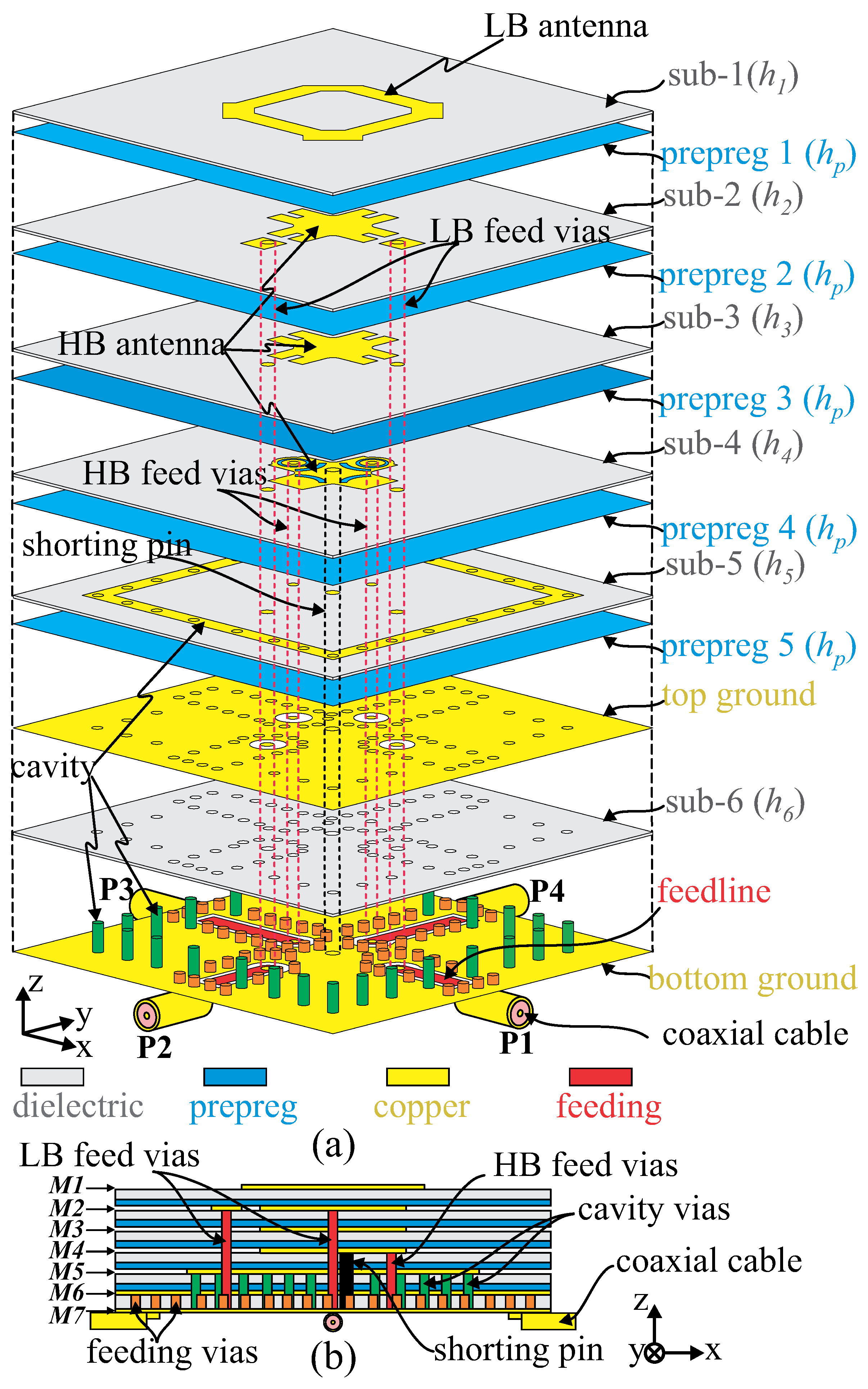
2. Antenna Design and Working Mechanism

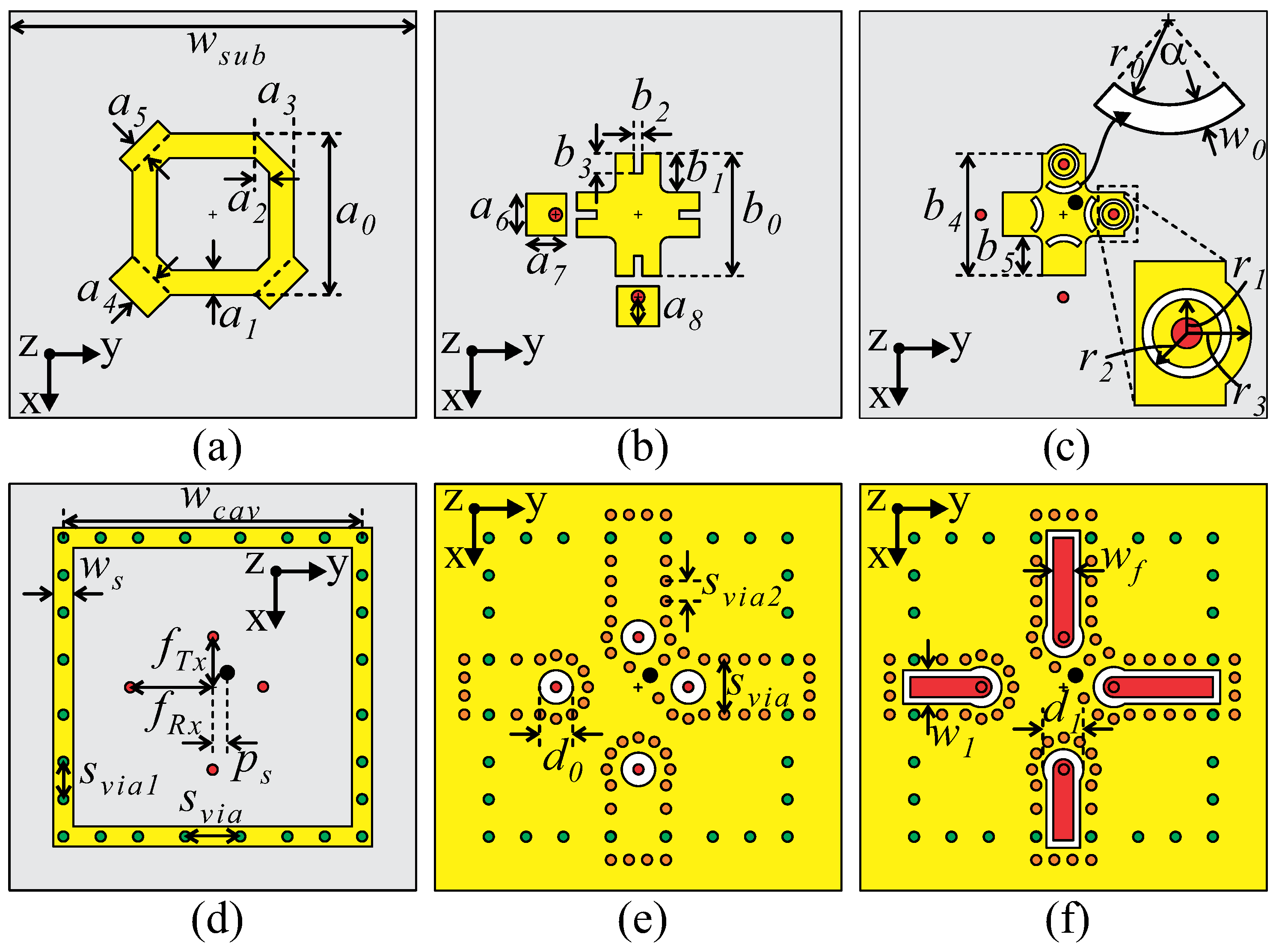
2.1. Antenna Configuration

The geometry of the proposed four-port shared-aperture DBDP antenna and its side view are shown in Figure 1a,b, respectively. The antenna is designed with a multilayer PCB process. It has six substrate layers (sub-1–sub-6), five prepreg layers (prepreg 1–5), and seven copper layers (M1–M7). The substrates are Taconic TLE-95 ( ε 1 = 2.95 and tan δ 1 = 0.0028). The prepreg materials have the same thickness of h p and are based on Rogers RO4450T material ( ε 2 = 3.23 and tan δ 2 = 0.0039).
The dual-band operation of the proposed antenna is achieved by two separate antennas, one LB antenna and one HB antenna, sharing a common radiating aperture. The LB antenna consists of a square-ring radiator with four chamfered corners printed on the copper layer M1. Two L-probe feeds, each comprising a stripline embedded in copper layer M2 and an LB feed, are implemented and positioned in the x- and y-directions to excite the square ring for dual polarization at the low band. In order to improve the impedance matching of the LB antenna, three protruding stubs are attached directly to the corners of the square ring. The HB antenna is a stacked-patch radiator, consisting of two identical plus-shaped parasitic patches printed on the copper layers M2 and M3 and a plus-shaped driven patch printed on the copper layer M4. Two capacitive feeds are used and positioned in the x- and y-directions to excite the driven patch for dual polarization at the high band. Four identical open rectangular slots are etched symmetrically on each parasitic patch to lower the operational frequency band of the HB antenna. In addition, four identical arc-shaped slots are etched symmetrically on the driven patch to improve the impedance matching. Due to the inherently poor isolation of the capacitive feeding, the HB antenna is equipped with a shorting pin to improve the isolation between two orthogonal polarizations. The proposed antenna is excited by four excitation ports P1P4 through four 50- Ω coaxial cables. Each coaxial cable is connected to a feed via a grounded coplanar waveguide (GCPW) consisting of a feedline and a bottom ground plane on the copper layer M7, a top ground plane on the copper layer M6, and a series of orange blind vias penetrating through the substrate layer sub-6. A cavity formed by a square ring printed on the copper layer M5 and a series of green blind vias surrounding the antenna is used to define the array lattice size for array construction. The size of the cavity is 10.3 mm × 10.3 mm. This corresponds to an array with spacing of 0.43 λ 12.75 GHz and 0.50 λ 14.5 GHz between elements at 12.75 and 14.5 GHz, respectively, allowing a maximum achievable scan angle of ±70° for both operating bands. The detailed configurations of each copper layer are shown in Figure 2, with the optimized design parameters summarized in the caption. The antenna was optimized using Ansys HFSS 2020 R2.

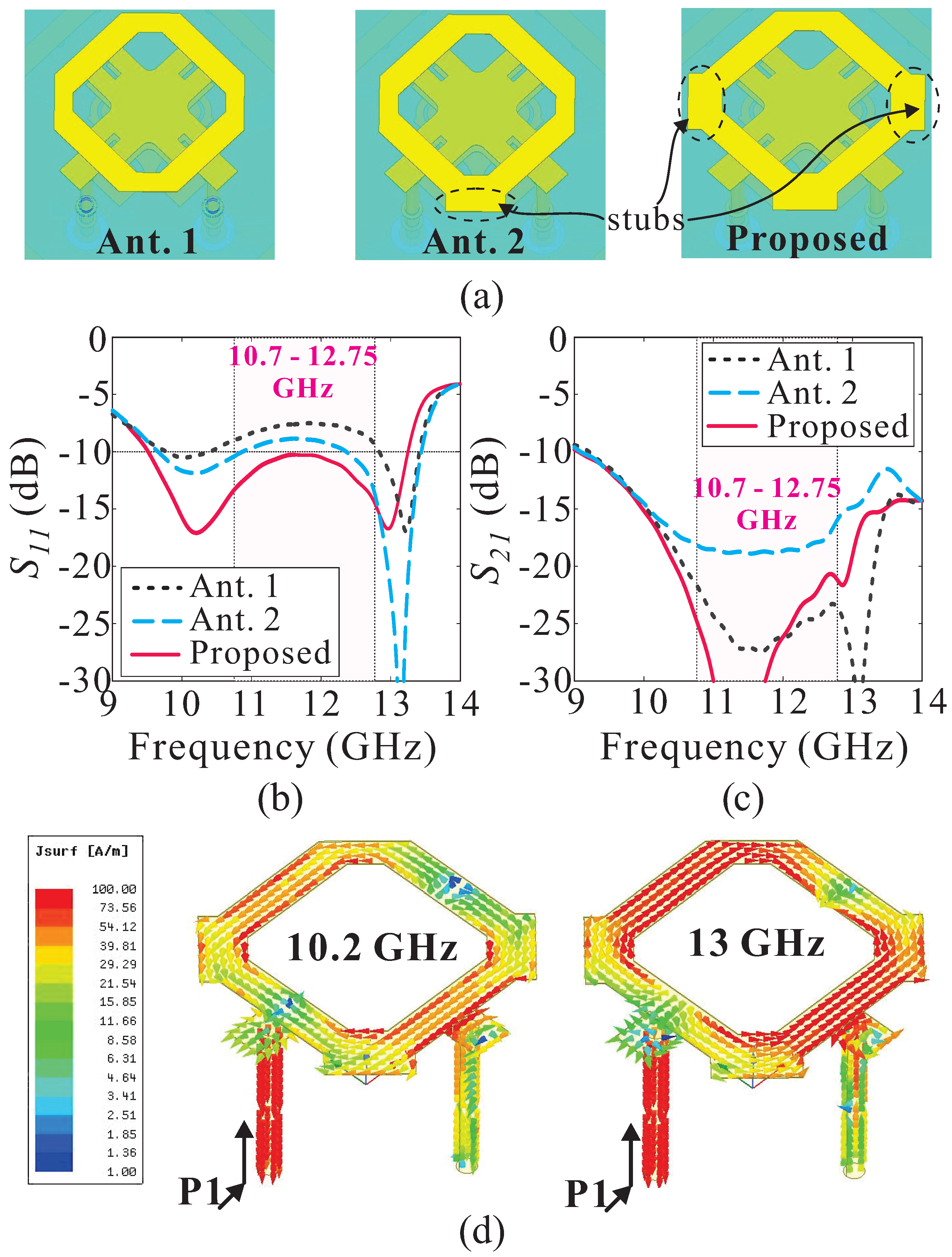
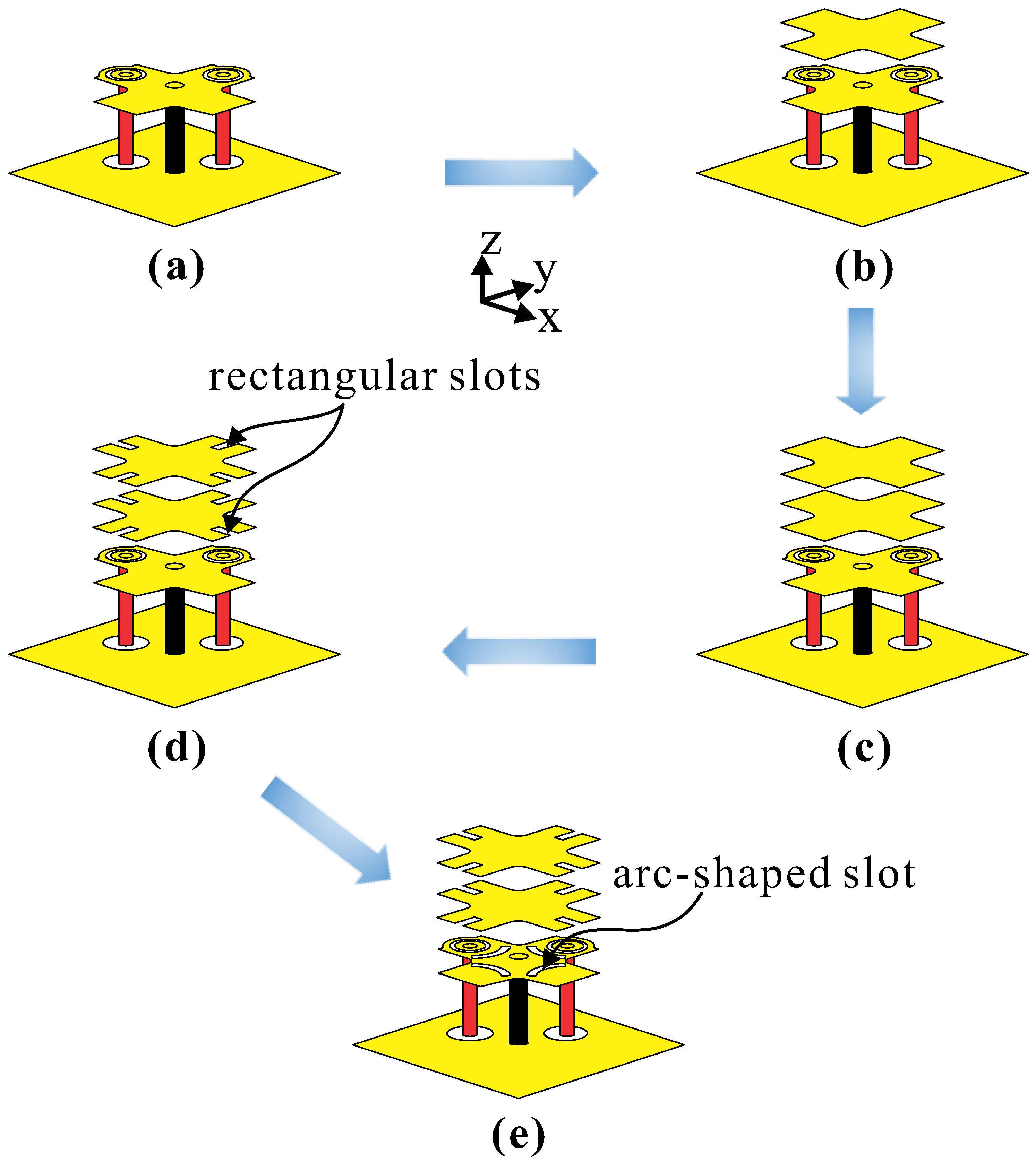
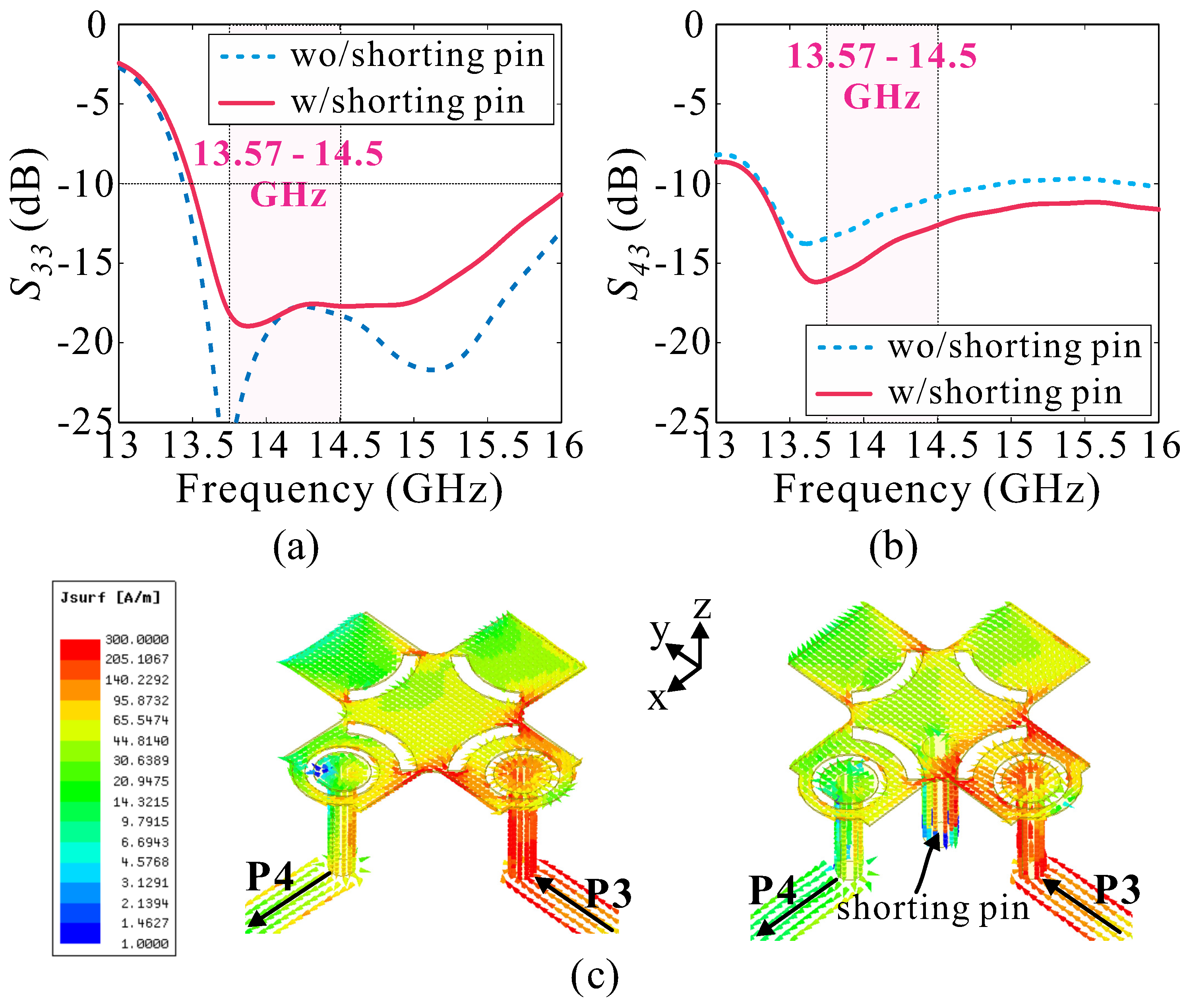
2.2. Working Mechanism

The proposed antenna is developed based on the design concept presented in [15]. This antenna, however, has a large size and a high frequency ratio of approximately 2. Therefore, this work aims to design a compact shared-aperture DBDP antenna with a smaller frequency ratio in order to meet the requirements for the downlink and uplink bands of the Ku band. The following sections describe the key steps involved in designing the proposed antenna.
Figure 3a illustrates the design steps for the LB antenna. Two reference designs, including Ant.1 with no protruding stub and Ant.2 with one protruding stub, are also investigated to compare with the proposed one. The simulated | S 11 | and | S 21 | are shown in Figure 3b,c, respectively. As observed, the protruding stubs help to improve the impedance matching of the LB antenna significantly (see Figure 3b). Moreover, high isolation between two orthogonal polarizations | S 21 | of the LB antenna is retained mostly by implementing three protruding stubs (see Figure 3c). Referring to Figure 3a, the LB antenna exhibits a −10 dB impedance bandwidth (IBW) covering the entirety of the desired frequency band of 10.7–12.75 GHz. The simulated current distributions observed at two resonant frequencies of 10.2 GHz and 13 GHz when the LB antenna is excited by P1 are illustrated in Figure 3d. At each resonant frequency, two currents appear, one in the clockwise direction and another in the anti-clockwise direction, demonstrating the fundamental T M 11 mode operating over the operating bandwidth [18,19].
The HB antenna is designed according to the procedure shown in Figure 4, and the simulated | S 33 | of the HB antenna according to each procedure is shown in Figure 5 (the S-parameters of the LB antenna are not shown here for brevity). In addition, the simulation showed that the HB antenna design procedure had a minor impact on the LB antenna’s performance. As a starting point, a capacitive fed microstrip patch antenna (HB-Ant.1) is selected and designed as shown in Figure 4a. The miniaturization of the patch is achieved by cutting off four small squares from each corner. As shown in Figure 5, HB-Ant.1 exhibits poor impedance matching for the frequency of interest from 13.75 to 14.5 GHz. Thus, it is necessary to improve the impedance matching of HB-Ant.1. To improve the impedance matching, a plus-shaped parasitic patch is introduced and located above the driven patch of HB-Ant.2. As illustrated in Figure 5, the impedance matching of HB-Ant.2 is improved for the frequency range of 14.1–15.2 GHz. In HB-Ant.3, one more plus-shaped parasitic patch is added, significantly improving the reflection coefficients (see Figure 5). At this point, instead of increasing the patch sizes to extend the impedance matching range further to cover the frequency of 13.75–14.5 GHz, four rectangular slots are cut off from each parasitic patch of HB-Ant.4. The | S 33 | of HB-Ant.4 indicates that it operates from 13.6 to 15.7 GHz (see Figure 5). Moreover, the reflection coefficient of the driven patch is significantly enhanced by applying arc-shaped slots in the final step. Through the inclusion of additional slots, the compactness of the HB antenna can be achieved without increasing its physical dimensions. According to Figure 5, the proposed HB antenna shows a −10 dB IBW, covering the entire desired frequency range of 13.75–14.5 GHz.
An overview of the shorting pin’s function is also presented in Figure 6. As shown in Figure 6a, the HB antenna’s resonance does not change significantly as a result of the shorting pin. With the shorting pin, the HB antenna still exhibits a wideband operating frequency band covering the entire designed frequency range of the Tx band. According to Figure 6b, employing the shorting pin in the HB antenna improves the isolation between its two orthogonal polarization ports ( | S 43 | ). The current distribution of the HB antenna without and with the shorting pin at 14 GHz is illustrated in Figure 6c. Without the shorting pin, an induced current will occur when the HB antenna is excited through P3 and flow to P4 (see Figure 6c), thus resulting in poor isolation between two ports. The function of the shorting pin is to enhance the isolation by shorting this induced current. As shown in Figure 6c, a strong current is generated in the shorting pin, while the induced current on the feed via P4 becomes weaker.

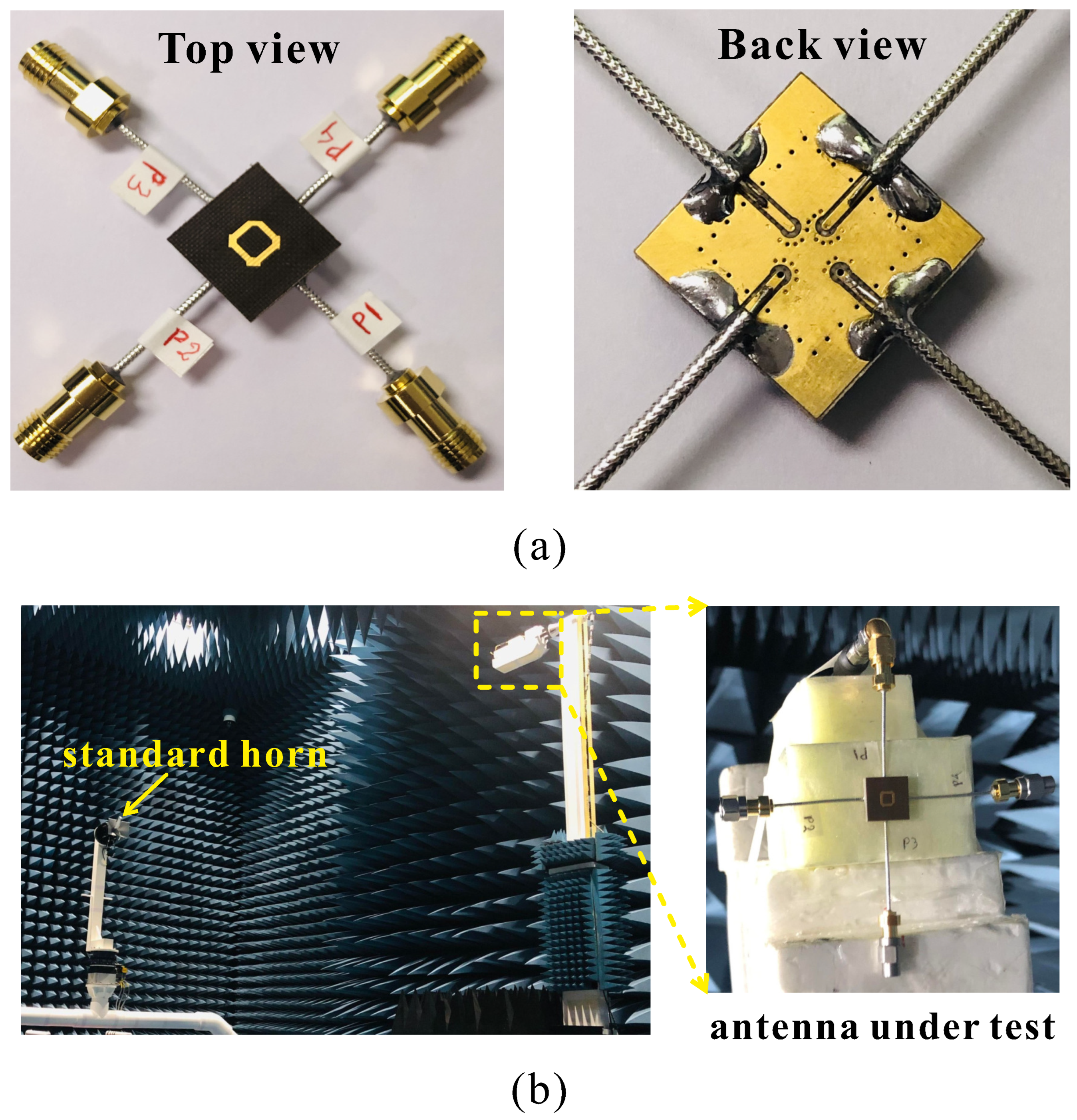
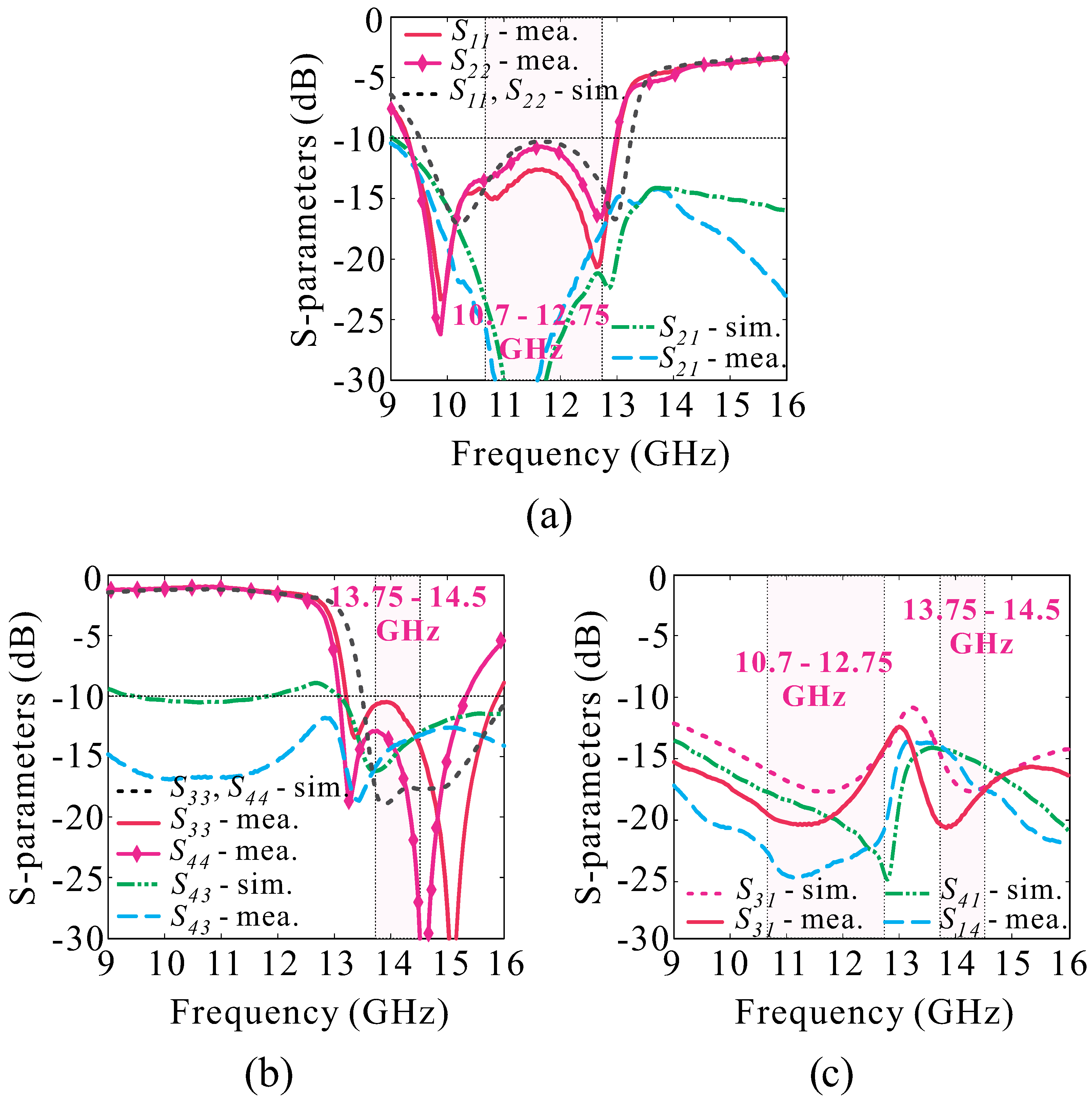
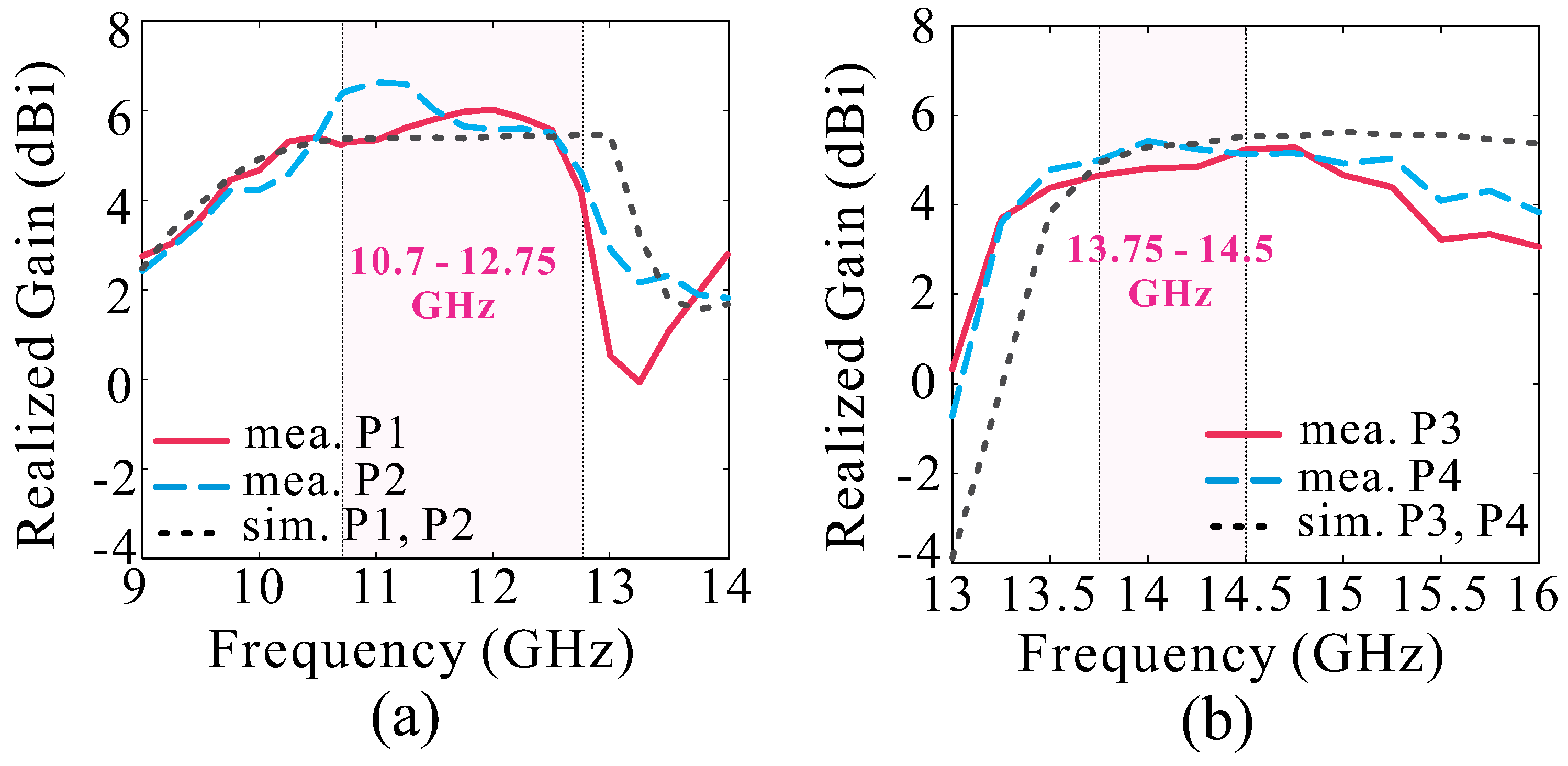
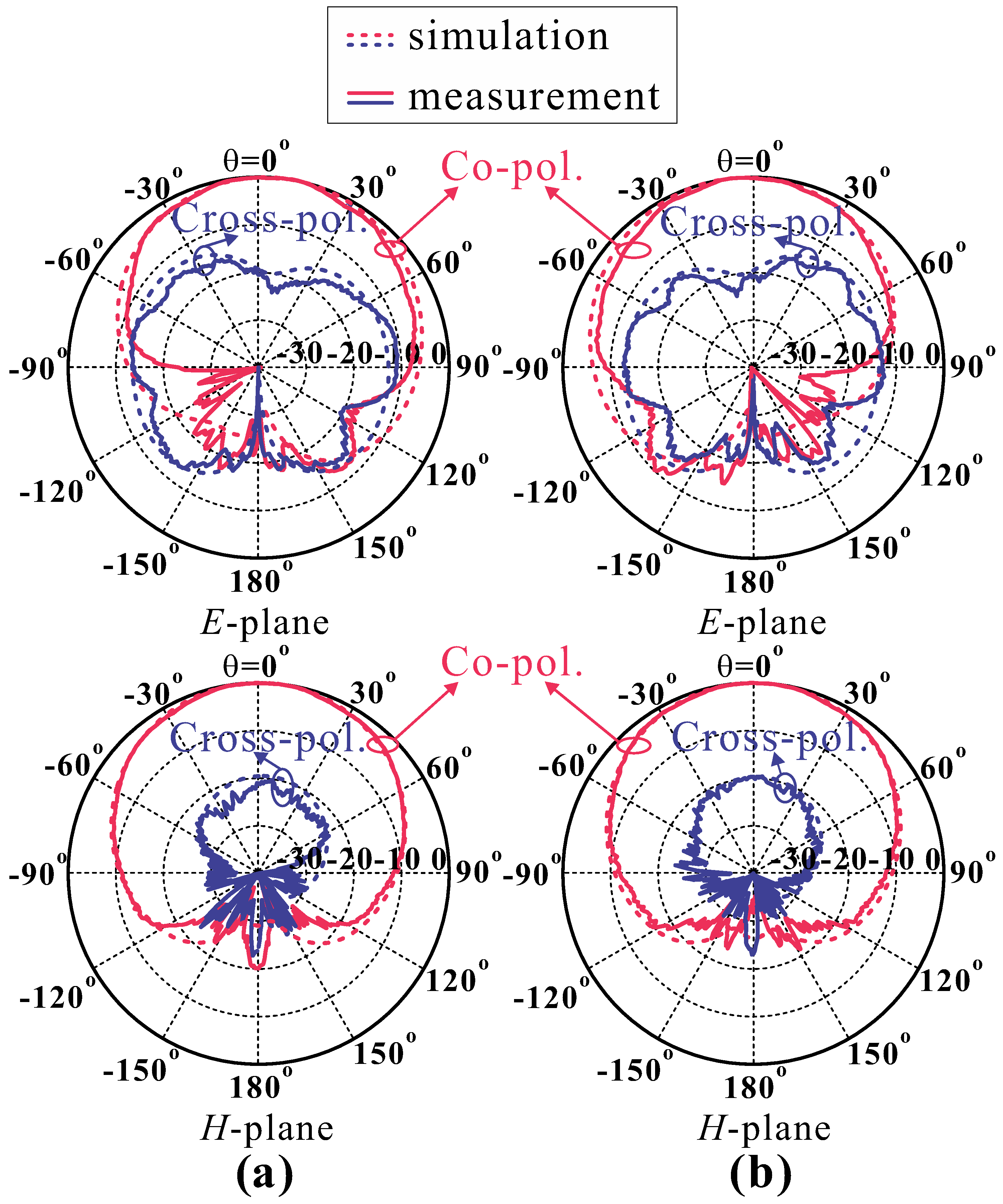
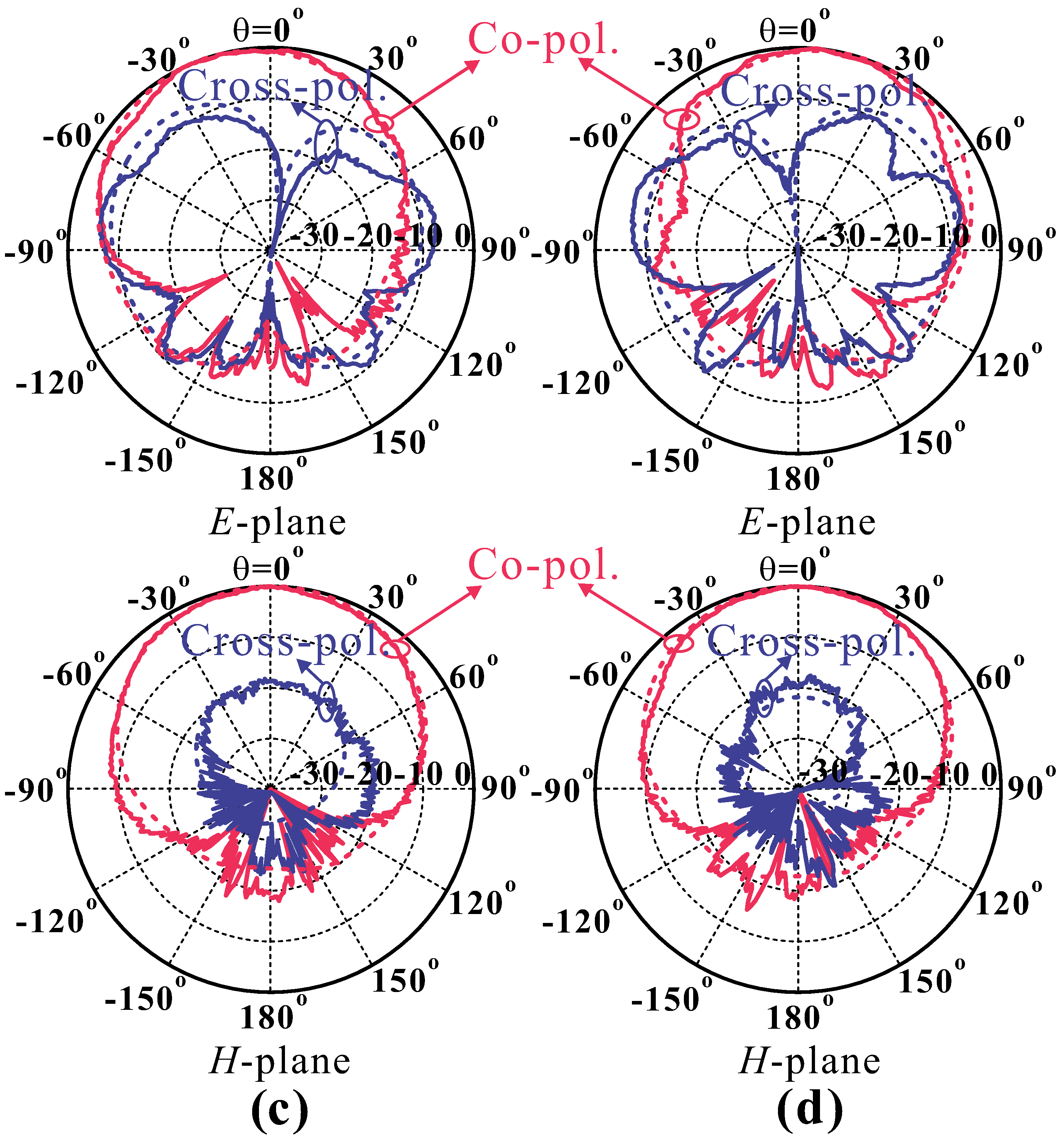
3. Experimental Results and Discussion

Based on the optimized design parameters, the proposed four-port shared-aperture DBDP antenna is fabricated with six Taconic TLE-95 substrate layers of different thicknesses. These substrate layers are bonded together using Roger RO4450T bonding sheets with the same thickness of 0.0762 mm. Figure 7a shows a photograph of the fabricated antenna. The antenna is 14.55 mm × 14.55 mm × 3.61 mm in size. Each excitation port of the antenna is connected with a semi-flexible pigtail cable (part number: SR047-KF1). The S-parameters were tested using the ShockLine™ MS46122B vector network analyzer from Anritsu. The far-field radiation characteristics of the fabricated antenna were measured in an RF anechoic chamber, as shown in Figure 7b. A dual-polarized rectangular horn antenna was utilized to attain the co-polarized/cross-polarized waves.
Figure 8a–c illustrate a comparison of the simulated and measured S-parameters of the proposed antenna. The simulation and measurement are found to be in reasonable agreement. The measured results are slightly shifted down approximately 300 MHz in comparison with the simulated results. Multilayer PCB manufacturing uncertainties are primarily responsible for this discrepancy. Referring to Figure 8a, the measured −10 dB IBW of 9.28–12.96 GHz (33.10%) is achieved for both P1 and P2 of the LB antenna, covering the entire Rx band of 10.7–12.75 GHz. Within the −10 dB IBW, the measured isolation between two orthogonal polarizations ( | S 21 | ) of the LB antenna is larger than 12 dB. Referring to Figure 8b, the measured −10 dB IBWs of the LB antenna are 13.21–15.88 GHz for P3 and 13.10–15.32 GHz for P4. Although the antenna is symmetrical, there is a discrepancy in the measured results of | S 33 | and | S 44 | , which is mainly caused by imperfections in the hand soldering process. An overlapped IBW of 13.21–15.32 GHz (14.79%) is achieved for the HB antenna, covering the whole Tx band of 13.75–14.5 GHz. Within the overlapped IBW, the measured isolation between two orthogonal polarizations ( | S 43 | ) of the HB antenna is larger than 12.4 dB. The Tx/Rx isolations, namely | S 31 | and | S 41 | , are depicted in Figure 8c. As observed, the measured Tx/Rx isolation of more than 14 dB is achieved in both the Rx band and Tx band.
The simulated and measured realized gains of the proposed antenna are depicted in Figure 9a,b. Within the Rx band, the measured realized gain ranges from 4.18 to 6.02 dBi for P1 and from 4.62 to 6.63 dBi for P2. Meanwhile, the measured realized gains of 4.99 to 5.42 dBi and 4.65 to 5.23 dBi are achieved for P3 and P4, respectively, within the Tx band. The measured and simulated radiation patterns of the proposed antenna in the xz-plane ( ϕ = 0°) and yz-plane ( ϕ = 90°) at 11.75 GHz (for Rx band) and 14 GHz (for Tx band) are plotted in Figure 10a–d. The measured cross-polarization in the boresight direction remains ≥20.1 dB and ≥18.4 dB in the Rx band and Tx band, respectively. It is also seen from Figure 10 that the off-axis cross-polarization in the E-plane is high, especially at 14 GHz (Tx band). Sequential rotated feeding can be applied to overcome this problem when designing a Tx/Rx dual-polarized phased-array antenna based on the proposed design. We compare the proposed antenna with previously reported DBDP antennas in Table 1. Compared to previous antennas [13,15,16], the proposed antenna has a smaller frequency ratio and a smaller size. The designs in [13,14] are two-port DBDP antennas, whereas the rest, including the proposed design, are four-port DBDP antennas. Although the design in [17] has a higher gain, the proposed antenna offers much wider IBWs and is much more compact.

4. Conclusions

A four-port shared-aperture DBDP antenna for Tx/Rx Ku-band SATCOM applications was developed, fabricated, and tested. The antenna was designed using the multilayer printed circuit board technology, consisting of an LB L-probe proximity-fed square-ring antenna and a HB stacked-patch antenna, sharing a common aperture. Through the experiment, an IBW of 9.28–12.96 GHz (13.21–15.32 GHz), an isolation value between two orthogonal polarizations of 12 dB (12.4 dB), and a peak gain of 6.63 dBi (5.42 diBi) were achieved at the low band (high band). The Tx/Rx isolation was more than 14 dB in both the Rx band and Tx band. The proposed antenna exhibits dual-band dual-polarized operation, covering two frequency bands, 10.7–12.75 GHz (Ku-band downlink) for Rx mode and 13.75–14.5 GHz (Ku-band uplink) for Tx mode; therefore, it can be directly used as a basic unit to develop a Ku-band Tx/Rx phased array for LEO SATCOM applications. This is considered the future work of the proposed design. In addition, the design can easily be scaled to operate in the Ka band (27.5–31 GHz for uplink and 17.7–21.2 GHz for downlink).

Author Contributions

Conceptualization, S.T.-V., W.Y.Y., H.W.C. and K.C.H.; methodology, S.T.-V. and K.C.H.; software, S.T.-V.; validation, S.T.-V., W.Y.Y., H.W.C. and K.C.H.; formal analysis, S.T.-V.; investigation, S.T.-V. and K.C.H.; resources, S.T.-V. and K.C.H.; data curation, S.T.-V., W.Y.Y., H.W.C. and K.C.H.; writing—original draft preparation, S.T.-V.; writing—review and editing, S.T.-V., W.Y.Y., H.W.C. and K.C.H.; visualization, S.T.-V.; supervision, K.C.H.; project administration, K.C.H. All authors have read and agreed to the published version of the manuscript.

Funding

This work was supported by the Research Fund of Hanwha Systems (Hanwha Phasor).

Institutional Review Board Statement

Not applicable.

Informed Consent Statement

Not applicable.

Data Availability Statement

All data have been included in study.

Conflicts of Interest

Authors Woo Yong Yang and Hyung Won Cho were employed by the The UK Office (Hanwha Phasor). The authors declare that this study received funding from Hanwha Systems (Hanwha Phasor). The funder was not involved in the study design, collection, analysis, interpretation of data, the writing of this article or the decision to submit it for publication.

References

  1. Gultepe, G.; Kanar, T.; Zihir, S.; Rebeiz, G.M. A 1024-element Ku-band SATCOM dual-polarized receiver with >10-dB/K G/T and embedded transmit rejection filter. IEEE Trans. Microw. Theory Tech. 2021, 69, 2484–3494. [Google Scholar] [CrossRef]
  2. Joo, T.; Hwang, C.; Park, J.; Kim, K.; Jung, J. Design of a tile-type Rx multi-beam digital active phased array antenna system. J. Electromagn. Eng. Sci. 2022, 22, 12–20. [Google Scholar] [CrossRef]
  3. Sandhu, A.I.; Arnieri, E.; Amendola, G.; Boccia, L.; Meniconi, E.; Ziegler, V. Radiating elements for shared aperture Tx/Rx phased arrays at K/Ka band. IEEE Trans. Antennas Propag. 2016, 64, 2270–2282. [Google Scholar] [CrossRef]
  4. Kang, Y.-G.; Kim, C.-K.; Park, S.-O. Ocean image formation algorithm using altimeter data for next generation satellite SAR. J. Electromagn. Eng. Sci. 2022, 22, 85–94. [Google Scholar] [CrossRef]
  5. Kim, S.; Nam, S. Design of a relocatable antenna element module for a Ku-band reconfigurable array with low mutual coupling. J. Electromagn. Eng. Sci. 2022, 22, 534–536. [Google Scholar] [CrossRef]
  6. Weily, A.R.; Nikolic, N. Dual-polarized planar feed for low-profile hemispherical Luneburg lens antennas. IEEE Trans. Antennas Propag. 2012, 60, 402–407. [Google Scholar] [CrossRef]
  7. Zaghloul, A.I.; Gunta, R.K.; Kohls, E.C.; Sun, L.Q.; Allnutt, R.M. Low cost flat antennas for commercial and military SATCOM terminals. In Proceedings of the MILCOM Communications for Network-Centric Operations: Creating the Information Force, McLean, VA, USA, 28–31 October 2001; Volume 2, pp. 795–799. [Google Scholar]
  8. Vaccaro, S.; Tiezzi, F.; Rúa, M.F.; De Ocr, C.D.G. Ku-band lowprofile Rx-only and Tx-Rx antennas for mobile satellite communications. In Proceedings of the 2010 IEEE International Symposium on Phased Array Systems and Technology, Waltham, MA, USA, 12–15 October 2010; pp. 536–542. [Google Scholar]
  9. Tiezzi, F.; Vaccaro, S. Hybrid phased array antenna for mobile KU-band DVB-S services. In Proceedings of the 2006 1st European Conference on Antennas and Propagation, Nice, France, 6–10 November 2006; pp. 1–4. [Google Scholar]
  10. Kim, I.; Lee, B. Wideband antenna for high-frequency 5G wireless communication. J. Electromagn. Eng. Sci. 2022, 22, 296–301. [Google Scholar] [CrossRef]
  11. Hwang, J.-H.; Lee, J.; Kim, K.-J.; Lee, H.L. A millimeter-wave GaN MMIC front end module with 5G NR performance verification. J. Electromagn. Eng. Sci. 2022, 22, 638–646. [Google Scholar] [CrossRef]
  12. Wu, F.; Xiang, L.; Jiang, Z.; Yu, C.; Hong, W. A wideband dual-polarized magneto-electric dipole antenna for millimeter wave applications. Microw. Opt. Technol. Lett. 2020, 63, 1452–1457. [Google Scholar] [CrossRef]
  13. Sun, W.; Li, Y.; Chang, L.; Li, H.; Qin, X.; Wang, H. Dualband dual-polarized microstrip antenna array using double-layer gridded patches for 5G millimeter-wave applications. IEEE Trans. Antennas Propag. 2021, 69, 6489–6499. [Google Scholar] [CrossRef]
  14. Yang, S.J.; Yao, S.F.; Ma, R.-Y.; Zhang, X.Y. Low-profile dual-wideband dual-polarized antenna for 5G millimeter-wave communications. IEEE Antennas Wirel. Propag. Lett. 2022. early access. [Google Scholar] [CrossRef]
  15. Sharma, D.K.; Kulshrestha, S.; Chakrabarty, S.B.; Jyoti, R. Shared aperture dual band dual polarization microstrip patch antenna. Microw. Opt. Technol. Lett. 2013, 55, 917–922. [Google Scholar] [CrossRef]
  16. Pandey, B.K.; Chakrabarty, S.B.; Jyoti, R. Common aperture dual-band dual-polarized planar microstrip antenna. IETE J. Res. 2018, 64, 489–496. [Google Scholar] [CrossRef]
  17. Catalani, A.; Toso, G.; Angeletti, P.; Albertini, M.; Russo, P. Development of enabling tecnologies for Ku-band airborne SATCOM phased-arrays. Electronics 2020, 9, 488. [Google Scholar] [CrossRef]
  18. Guo, Y.-X.; Luk, K.-M.; Lee, K.-F. L-probe proximity-fed annular ring microstrip antennas. IEEE Trans. Antennas Propag. 2001, 49, 19–21. [Google Scholar]
  19. Wong, K.-L.; Chenk, J.-Z.; Li, W.-Y. Four-port wideband annular-ring patch antenna generting four decoupled waves for 5G multi-input-multi-ouput access points. IEEE Trans. Antennas Propag. 2021, 69, 2946–2951. [Google Scholar] [CrossRef]
Figure 1. Geometry of the proposed four-port shared-aperture DBDP antenna. (a) 3D exploded view. (b) Side view. ( h 1 = 0.13 mm, h 2 = 0.25 mm, h 3 = 1.58 mm, h 4 = h 5 = 0.51 mm, h 6 = 0.25 mm, and h p = 0.076 mm).
Applsci 14 02730 g001
Figure 2. Detailed configurations of each copper layer. (a) Copper layer M1. (b) Copper layer M2. (c) Copper layer M4. (d) Copper layer M5. (e) Copper layer M6. (f) Copper layer M7. (Unit: mm, a 0 = 4.82, a 1 = 0.735, a 2 = 0.45, a 3 = 1.135, a 4 = 0.5, a 5 = 0.35, a 6 = 0.8, a 7 = 0.86, a 8 = 0.6, b 0 = 3.66, b 1 = 1.16, b 2 = 0.25, b 3 = 0.65, b 4 = 3.63, b 5 = 1.16, r 0 = 0.73, r 1 = 0.34, r 2 = 0.44, r 3 = 0.64, w 0 = 0.2, w s = 0.6, w c a v = 10.3, p s = 0.3, s v i a = 1.645, s v i a 1 = 1.115, f R x = 2.46, f T x = 1.46, s v i a 2 = 0.7, d 0 = d 1 = 1.2, w f = 0.6, w 1 = 1, w s u b = 14.57, α = 76°).
Applsci 14 02730 g002
Figure 3. (a) Design evolution of the LB antenna. (b) | S 11 | . (c) | S 21 | . (d) Simulated current distributions at 10.2 GHz and 13 GHz.
Applsci 14 02730 g003
Figure 4. Step-by-step antenna design for the HB antenna (other components are hidden for clear illustration). (a) HB-Ant.1. (b) HB-Ant.2. (c) HB-Ant.3. (d) HB-Ant.4. (e) Proposed HB antenna.
Applsci 14 02730 g004
Figure 5. Simulated | S 33 | for each step of the design procedure for the HB antenna.
Applsci 14 02730 g005
Figure 6. Effect of the shorting pin on the (a) | S 33 | and (b) | S 43 | of the HB antenna. (c) Simulated current distribution of the HB antenna with and without the shorting pin when P3 excited.
Applsci 14 02730 g006
Figure 7. Photograph of the (a) fabricated antenna and (b) far-field measurement environment.
Applsci 14 02730 g007
Figure 8. (a) S -parameters of the LB antenna. (b) S -parameters of the HB antenna. (c) Tx/Rx isolation.
Applsci 14 02730 g008
Figure 9. Simulated and measured realized gains of (a) LB antenna and (b) HB antenna.
Applsci 14 02730 g009
Figure 10. Simulated and measured normalized radiation patterns of the proposed antenna at (a) 11.75 GHz, fed by P1, (b) 11.75 GHz, fed by P2, (c) 14 GHz, fed by P3, and (d) 14 GHz, fed by P4.
Applsci 14 02730 g010aApplsci 14 02730 g010b
Table 1. Comparison with previous DBDP antennas.
Ref.IBWs
LB/HB [%]
Peak Gain
LB/HB [dBi]
Frequency
Ratio
Tx/Rx
Isolation
Size [ λ L 2 ]
[13] 23.7/12.8N.M.1.7>170.64 × 0.64
[14] 22/165.0/5.01.5N.M.50 × 0.50
[15]28.3/29.47.04/6.942.0N.M.0.83 × 0.83 ★★
[16] 8.0/10.08.7/8.32.0N.M.0.75 × 0.75
[17]13.7/5.3 ★★8.0/7.01.2>170.86 × 0.86
Proposed33.10/14.796.63/5.421.2>140.56 × 0.56
λ L is the free space wavelength at the center frequency of the low band. Simulated. ★★ Estimated from graph. N.M.: not mentioned.
Disclaimer/Publisher’s Note: The statements, opinions and data contained in all publications are solely those of the individual author(s) and contributor(s) and not of MDPI and/or the editor(s). MDPI and/or the editor(s) disclaim responsibility for any injury to people or property resulting from any ideas, methods, instructions or products referred to in the content.

