Article

Graphene-Enhanced CuW Composites for High-Voltage Circuit Breaker Electrical Contacts

1
State Key Laboratory of Advanced Power Transmission Technology, State Grid Smart Grid Research Institute Co., Ltd., Beijing 102209, China
2
State Key Laboratory for Mechanical Behavior of Materials, Xi’an Jiaotong University, No. 28 Xianning West Road, Xi’an 710049, China
*
Author to whom correspondence should be addressed.
Appl. Sci. 2024, 14(7), 2731; https://doi.org/10.3390/app14072731
Submission received: 21 February 2024 / Revised: 20 March 2024 / Accepted: 21 March 2024 / Published: 25 March 2024
(This article belongs to the Special Issue Advanced Methodology and Analysis in Electrical Materials Science)

Abstract

:

Featured Application

The innovative graphene-enhanced CuW composites can be applied to 252~1100 kV high-voltage circuit breakers to improve the breaking capacity of high-voltage circuit breakers.

Abstract

To address the issue of over-standard short-circuit currents in a power system, it is imperative to enhance the comprehensive performance of the electrical contacts, which serve as the lynchpin of circuit breakers, so as to improve the breaking capacity of high-voltage circuit breakers. Graphene, as the most prominent two-dimensional carbon material in recent years, has garnered widespread applications across various fields. In this study, graphene-enhanced CuW composites for high-voltage circuit breaker electrical contacts were prepared innovatively using integrated vacuum infiltration technology. The innovative graphene-enhanced CuW composites significantly improved the mechanical, electrical, and ablation resistance properties, and have been successfully applied in the 252 kV/63 kA high-voltage SF6 circuit breakers, achieving 20 times effective consecutive full-capacity short-circuit current breaking. It provides a new route for the development and application of high-performance CuW electrical contacts. Looking ahead, it is planned to extend their application to higher voltage grade high-voltage circuit breakers.

1. Introduction

Electrical contacts, being the pivotal component of high-voltage circuit breakers, directly influence their breaking capacity [1,2,3]. Copper–tungsten (CuW) composites, as a prototypical two-phase pseudo-alloy, integrate the high conductivity and thermal conductivity of copper with the exceptional strength and arc ablation resistance of tungsten. Owing to these advantageous characteristics, CuW composites, especially CuW80 (80 wt.% W content), are extensively utilized as electrical contacts in high-voltage circuit breakers [4,5,6,7,8].
However, with the development of New Power System, the increasingly serious problem of over-standard short-circuit current leads to higher requirements for the breaking capacity of high-voltage circuit breakers [9,10,11,12,13,14]. Traditional CuW composites find it difficult to meet the higher requirements of electrical contacts for comprehensive properties such as conductivity and arc ablation resistance. It is urgent to improve the comprehensive properties of CuW composites through process optimization or doping modification to meet the needs of higher voltage grade circuit breakers.
To improve the properties of CuW composites, doping modification by the third component such as rare earth elements, rare earth element oxides (La2O3, ThO2, CeO2) or ceramic materials (Al2O3, Y2O3), and other third phase elements was always used. By doping modification, the thermochemical stability of CuW composites was improved through the uniform dispersion of additive. However, the addition of the third component may bring some other problems, such as the significant decrease in electrical conductivity [15,16,17,18,19,20,21,22]. It is unable to achieve the coordinated improvement of the comprehensive performance. Graphene, as a new two-dimensional carbon material rising in recent years, has remarkable advantages such as high electrical conductivity, high thermal conductivity, high specific surface area, light weight, and high strength [23,24,25,26,27,28,29,30]. It will be an ideal material for the modification of CuW composites, and is expected to bring more excellent comprehensive properties as an additive modification phase.
In previous studies, Duan J. et al. [18] systematically investigated the arc ablation behavior of Cu–W alloys with different W contents in an atmospheric environment. Li J. and Luo L. et al. [19,20] investigated the physical and mechanical properties of W–Cu alloys doped with rare-earth oxides La2O3. Yang X. et al. [21] prepared W–Cu alloys with an individual addition of WC and CeO2 particles, and found that a good combination of the hardness, electric conductivity, and dielectric strength of W–Cu alloys can be obtained with proper amount of WC or CeO2 addition into the tungsten skeleton. Mu Z. et al. [22] found that the hardness and density of copper-based contact materials increase with adding proper amount of Y2O3. In this paper, graphene-enhanced CuW composites and electrical contacts for a high-voltage circuit breaker were prepared innovatively using integrated vacuum infiltration technology. Different from rare-earth oxides or ceramic particles doping modification, graphene would not affect the electrical and thermal conductivity properties of CuW composites when used as an additive [30]. The innovative graphene-enhanced CuW electrical contacts passed type testing and realized engineering application relying on the high-voltage circuit breaker for the first time, which provides a new route for the development and application of high-performance CuW electrical contacts.

2. Materials and Methods

2.1. Raw Materials

Tungsten powder and copper powder are utilized as raw materials for the compression of tungsten skeleton, while copper alloy ingots are primarily employed as raw materials for vacuum infiltration. In this study, the commercially available tungsten powder (average particle size 4~8 μm, oxygen content ≤ 600 ppm, purity ≥ 99.9%), electrolytic copper powder (particle size 50 mm, oxygen content ≤ 500 ppm, purity ≥ 99.9%), and copper alloy ingot (QCr0.5) were all purchased from Henan Kefeng New Material Co., Ltd., Zhengzhou, China.
The graphene used in this study is reduced graphene oxide (rGO), which not only possesses the exceptional properties, but also exhibits favorable economic performance, thereby being employed as the reinforced doping material. It is typically prepared through an electrothermal reduction process, aiming to eliminate the oxygen-containing functional groups present on the graphene oxide surface [23,24]. In this study, commercially available rGO (specific surface area 500 ± 50 m2/g, oxygen content ≤ 15%, transverse dimension 20 μm, thickness ≤ 5nm) was used, which purchased from Jiangsu Xianfeng Nanomaterials Technology Co., Ltd., Nanjing, China.

2.2. Equipment

2.2.1. Powder Mixing

The raw material powder mixing process was performed using a 3D high-energy planetary ball mill. To address the issue of uneven distribution of copper–tungsten–graphene mixed powder resulting from density and volume deviations, a combination of multi-dimensional high-energy mixing and multiphase addition technology was employed. This approach ensured the uniform dispersion and distribution of graphene within the copper–tungsten mixed powder.

2.2.2. Isostatic Pressing

The porous tungsten skeleton blanks are pressed using a cold isostatic press with the mixed raw material powder placed inside the rubber sleeve of the mold. By applying an appropriate pressure and holding time (300~400 MPa, 5~10 min), tungsten skeleton blanks can be achieved that exhibit excellent apparent quality, uniform density, and the absence of delamination.

2.2.3. Vacuum Infiltration

The vacuum infiltration sintering process is meticulously conducted within a vacuum infiltration furnace, which is specifically designed to offer a controlled environment for the infiltration of liquid copper into the tungsten skeleton.
The vacuum infiltration furnace is equipped with advanced technology that maintains a vacuum negative pressure environment of 10−2 Pa. This high vacuum ensures that there are minimal impurities and gases present during the infiltration process, which can potentially interfere with the penetration of the liquid copper.
Moreover, the furnace is capable of reaching temperatures exceeding 1500 °C, providing the necessary thermal energy for the infiltration process. The high temperature environment promotes the flow and wetting behavior of the liquid copper, enabling it to penetrate deeply into the pores and interstices of the tungsten skeleton. To further ensure the effectiveness of the infiltration process, the vacuum infiltration furnace employs a gradient heating program to gradually increases the temperature, which allows the liquid copper to infiltrate the tungsten skeleton uniformly and without causing any thermal stress or damage.
By combining the high vacuum controlled heating program and the liquid copper’s wetting properties, the vacuum infiltration sintering process ensures that the liquid copper fully penetrates into the depth of the tungsten skeleton. This not only enhances the compactness of the material, but also improves its mechanical strength, electrical conductivity, and thermal stability, making it suitable for a wide range of applications.

2.3. Preparation Process of CuW/Graphene-Enhanced CuW Composites and Electrical Contacts

Existing processes for the preparation of copper-based contact materials include: induced copper powder fusion infiltration, pre-sintered tungsten skeleton fusion infiltration, activation sintering, high-temperature liquid-phase sintering, vacuum sintering, and injection molding sintering. The microstructures of CuW composites produced under different process conditions are very different, and their comprehensive properties are therefore significantly different [4,5,6,7].
Tungsten possesses a high melting point of 3410 °C, and its sintering performance is inadequate below 1700 °C. Additionally, due to its low density and high hardness, the molding performance of tungsten is subpar, making it challenging to directly mold CuW composites with the desired high tungsten content and density of the tungsten skeleton. Consequently, the incorporation of induced copper powder remains the most widely utilized method for the preparation of CuW composites.
The induced copper powder fusion infiltration method is to add a certain proportion of induced copper powder during the preparation of tungsten skeleton blanks. Due to the good plasticity of copper, porous CuW skeleton blanks with desired strength and density can be fabricated. During the melting sintering process, the capillary phenomenon facilitates the infiltration of molten liquid copper into the porous tungsten skeleton. The copper then flows through the pores, gradually filling the tungsten skeleton, ultimately yielding CuW composites with superior overall performance.
In this study, the graphene-enhanced CuW composites were prepared by integrated vacuum infiltration technology, as shown in Figure 1. The raw materials used include tungsten powder, induced copper powder, copper alloy ingots for infiltration, and reduced graphene oxide nanosheets. The preparation process proceeded as follows: tungsten powder, inducing copper powder, and reducing graphene oxide powder were weighted in the appropriate proportions. Subsequently, paraffin and forming agent were added, and the mixture was thoroughly stirred and blended. Following this, the mixture was vacuum-dried at 80 °C. After sieving, the powder blend was loaded into a rubber sleeve and uniformly compacted. The porous skeleton blanks were obtained through isostatic pressing. Tungsten skeleton blanks and copper alloy ingots were stacked within a specially designed graphite mold. Subsequently, vacuum infiltration sintering was conducted at a temperature exceeding the melting point of copper (1350 °C) under a vacuum of 10−2 Pa. This allowed the liquid copper to fully infiltrate the porous tungsten skeleton, resulting in the production of a uniform and dense graphene-enhanced CuW composite. Liquid copper can fully infiltrate into the tungsten porous skeleton, and a uniform and dense graphene-enhanced CuW composite was obtained. The composite composition consisted of 20 wt.% copper and 0.02 wt.% graphene, with the remainder being tungsten. Finally, the electrical contact products were machined precisely in accordance with designated drawings and tailored to meet the specific design requirements of various circuit breakers.
The preparation process utilized for the CuW composites and the electrical contact products compared in this study followed the same aforementioned methodology, with the exception that the initial powder mixing stage, did not involve the addition of graphene. As a result, CuW composites with a copper content of 20 wt.% were ultimately obtained.

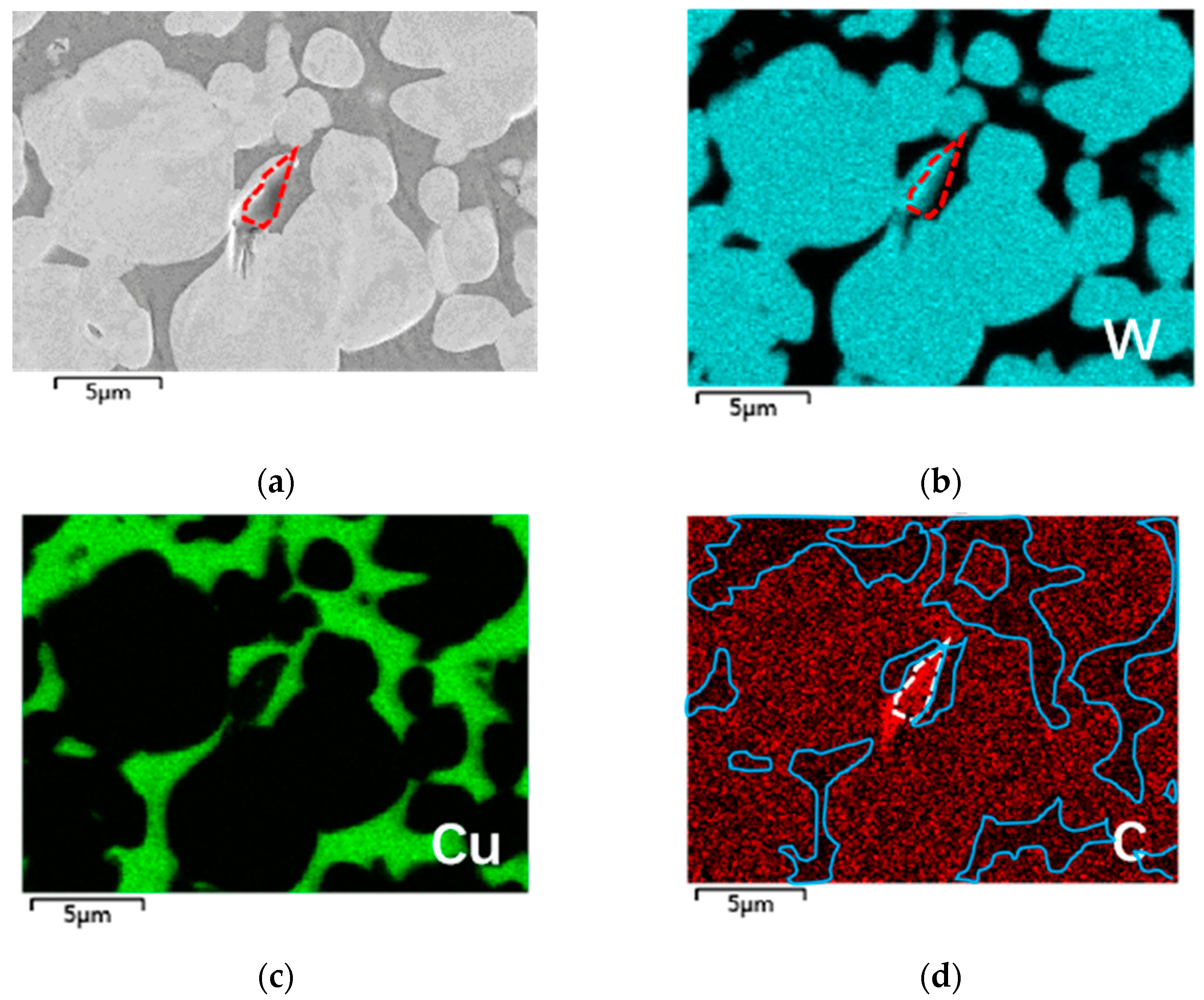
2.4. Microstructure Characterization Methods

2.4.1. Scanning Electron Microscope (SEM) Observation

The Scanning Electron Microscope (SEM) operates on the principle of generating and manipulating a focused beam of high-energy electrons to interact with a sample’s surface, thereby generating various signals (secondary electrons, reflected electrons, X-rays, etc.) that are subsequently detected and converted into visual images. The intensity of these signals is related to the properties of the sample’s surface, such as topography, composition, and crystal structure. Consequently, it facilitates the observation and analysis of the microstructure, composition, and other material properties with remarkable precision [31].
The microstructure of CuW composites, both prior to and following the addition of graphene, was observed utilizing a SUPRA55 (ZEISS, Jena, Germany) type scanning electron microscope. This allowed for a comparative analysis of the grain size and microstructure between the two samples, thereby elucidating the impact of graphene addition on the microstructure. Additionally, energy dispersive spectroscopy (EDS) was employed to observe and analyze the elemental distribution of Cu, W, and C within the material.

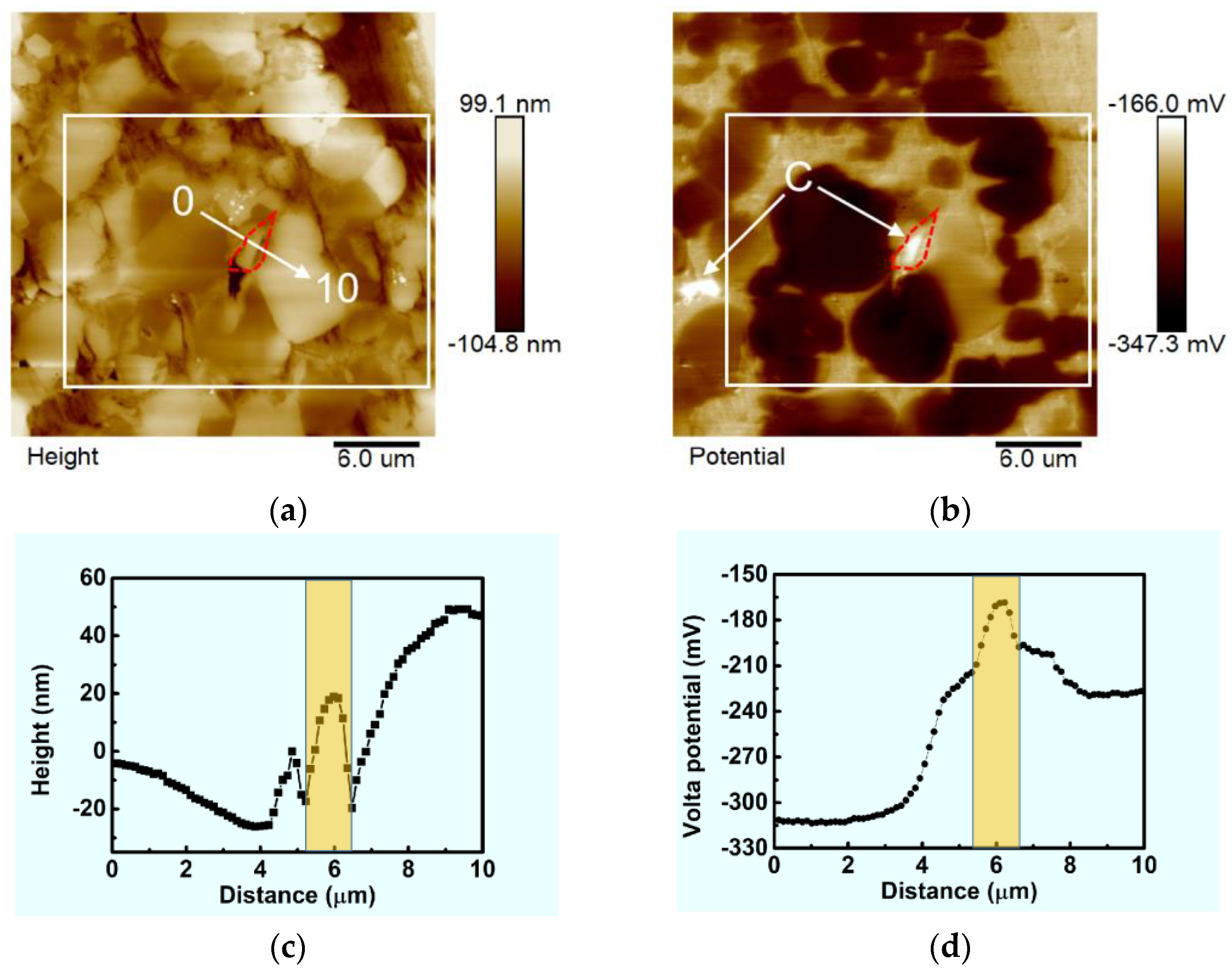
2.4.2. In Situ Scanning Kelvin Probe Force Microscopy (SKPFM) Experiment

An atomic force microscope (AFM) is a scanning probe microscope used to image and manipulate surfaces on an atomic scale. It works by scanning the surface of a sample using a sharp probe tip and measuring the force between the tip and the surface. These measurements yield high-resolution images of the sample’s surface, along with quantifications of surface roughness and other pertinent physical properties. Among the various modes of AFM, scanning Kelvin probe force microscopy (SKPFM) stands out as a technique capable of detecting the Volta potential of materials [32].
The AFM and SKPFM experiments were conducted using the TI-900 Triboindenter (Hysitron, Minneapolis, MN, USA) atomic force in situ test system and the Nanoscope V (Veeco, Plainview, NY, USA) equipped with the NT-MDT Kelvin probe, operating in the tapping mode. The surface height and Volta potential difference (hereinafter referred to as “potential” in the main text) of the materials were obtained in situ before and after the addition of graphene. By observing and analyzing the distribution and changing rules of surface height and potential, along with considering the disparities in the electronic work function among different elements, we were able to determine the distribution of graphene within the composites. The cantilever used in our study has a spring constant of 2.8 N·m−1, a resonant frequency of 60–100 kHz, and a standard PtIr-coated silicon tip with a <25 nm curvature. Lift height was set to 60 nm. The SKPFM experiments were carried out in air at room temperature and relative humidity of 38 ± 1%. The system was calibrated by using a high-quality highly oriented pyrolytic graphite prior to the experiment to ensure the accuracy of the potential measurements.

2.4.3. Raman Spectroscopy

Raman spectroscopy is an analytical method based on the Raman scattering effect, which analyzes the scattering spectra that are different from the frequency of the incident light in order to obtain information about molecular vibration and rotation, and is applied to the study of molecular structure [33].
Raman spectra with 533 nm laser wavelength were collected to analyze the structural state of carbon and examine the existence of graphene in composites at room temperature using a inVia confocal Raman microscope (Renishaw, England) over a range of 100~3500 cm−1.

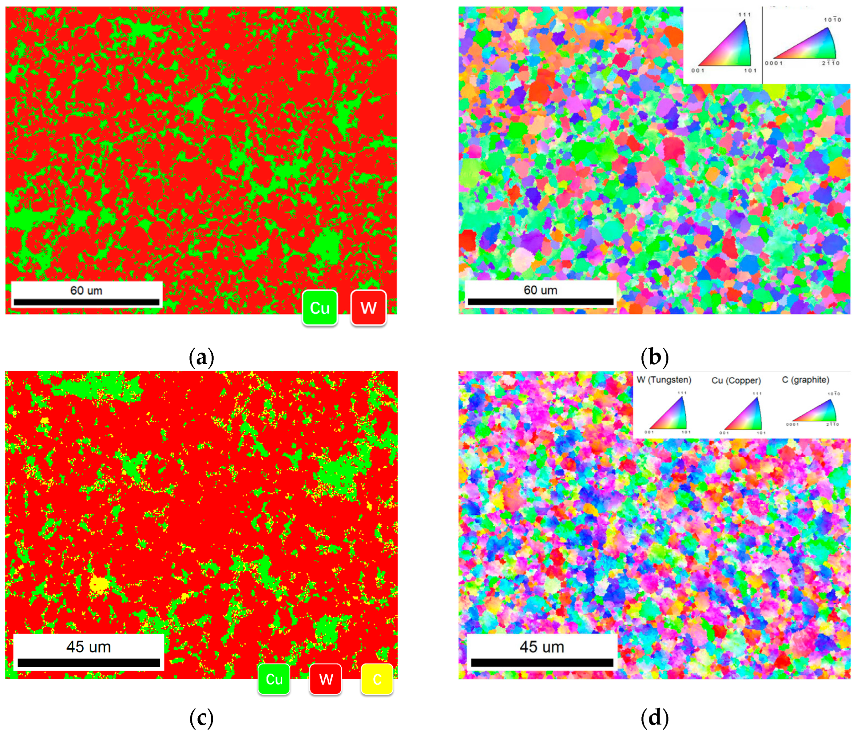
2.4.4. Electron Backscattered Diffraction (EBSD) Analysis

Backscattered electrons (BSE) are energetic electrons produced using elastic or inelastic scattering of an incident electron beam with the nucleus of an atom. Electron Backscattered Diffraction (EBSD) can be used to analyze the microstructure and orientation of solid crystalline materials.
Using a Thermo Scientific Helios 5 UX (Thermo Fisher Scientific, Waltham, MA, USA) focused ion beam electron microscope in combination with EBSD, the size and distribution of the phases prior to and following the addition of graphene were further observed, as well as the changes in the size and orientation of the grains. The possible effects of these changes on the properties were analyzed.

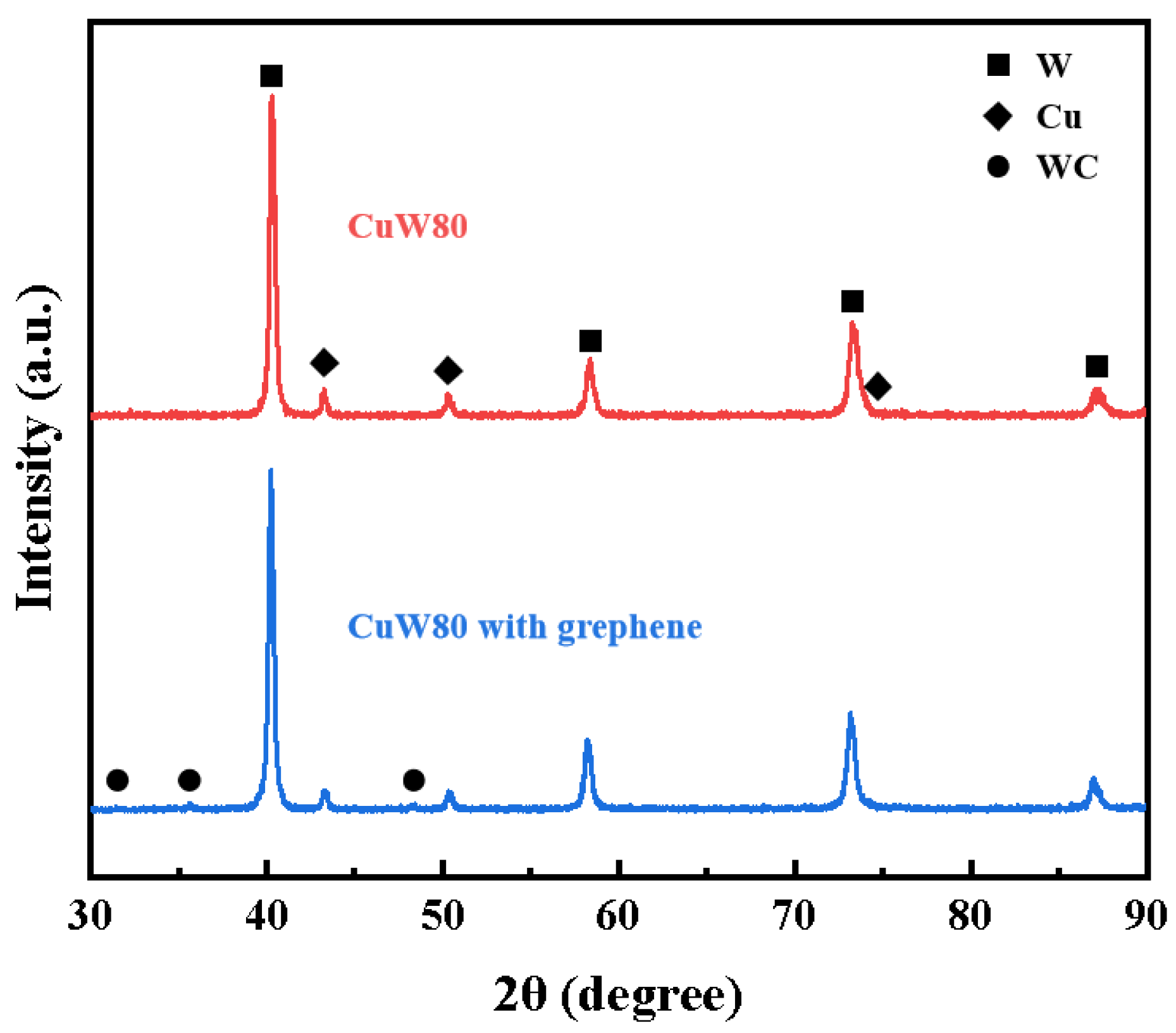
2.4.5. X-ray Diffraction (XRD) Analysis

The X-ray diffraction (XRD) investigations were carried out to identify phases in the CuW composites, both prior to and following the addition of graphene using X-ray Diffractometer (D/MAX-2600, Rigaku, Japan) operating at 40 kV and 40 mA with Cu Kα radiation and a scan rate of 0.02° s−1 in a 2θ range of 30°~90°.

2.5. Mechanical and Physical Property Testing Methods

The densities of the samples were determined, prior to and following the addition of graphene, through the application of the Archimedes principle with ultrapure water. Subsequently, the relative density of the samples were calculated using the theoretical density formula. The flexural strength was determined via a three-point bending test, utilizing an electronic universal testing machine, with the samples prepared as standard parts measuring 50 mm × 10 mm × 4 mm. The electrical conductivity of polished samples was evaluated by a digital metal conductivity meter at room temperature, with at least five measurements conducted for each specimen. A hardness test was conducted on the polished surface of the samples using a Brinell hardness tester, with a load of 750 kg and a dwell time of 30 s. All tests were rigorously conducted in accordance with the standard of ASTM B702 or GB/T 8320, ensuring that at least three samples of each composition underwent measurements to obtain an accurate average value.

2.6. Ablation Resistance Test

Full-capacity breaking tests were conducted in 252 kV/63 kA high-voltage circuit breakers using CuW80 contact materials prepared by the experimental process and CuW80 contact materials reinforced by adding graphene to compare the macroscopic morphology changes of the contacts as well as the dimensional changes after the experiments.

3. Results and Discussion

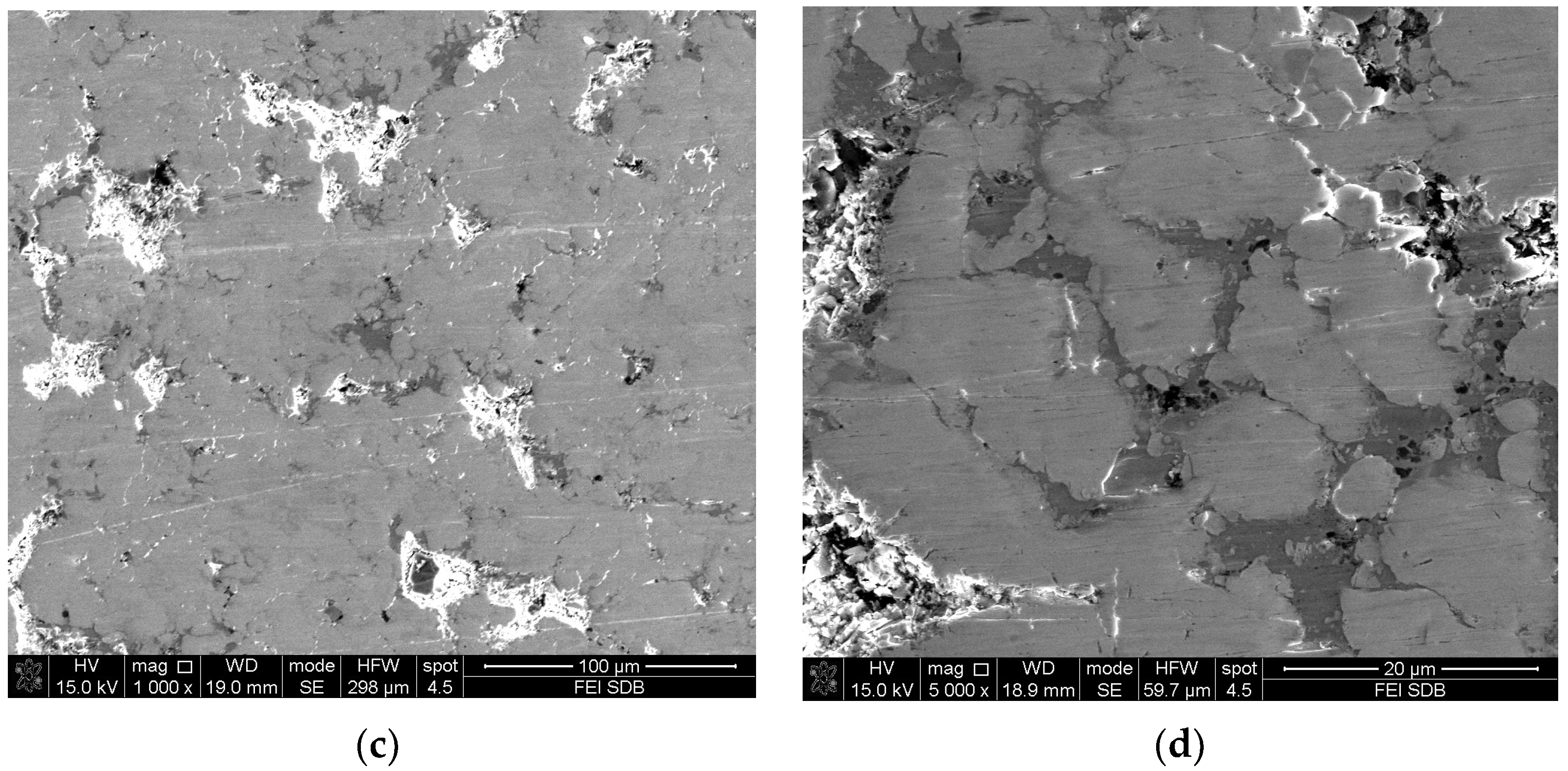
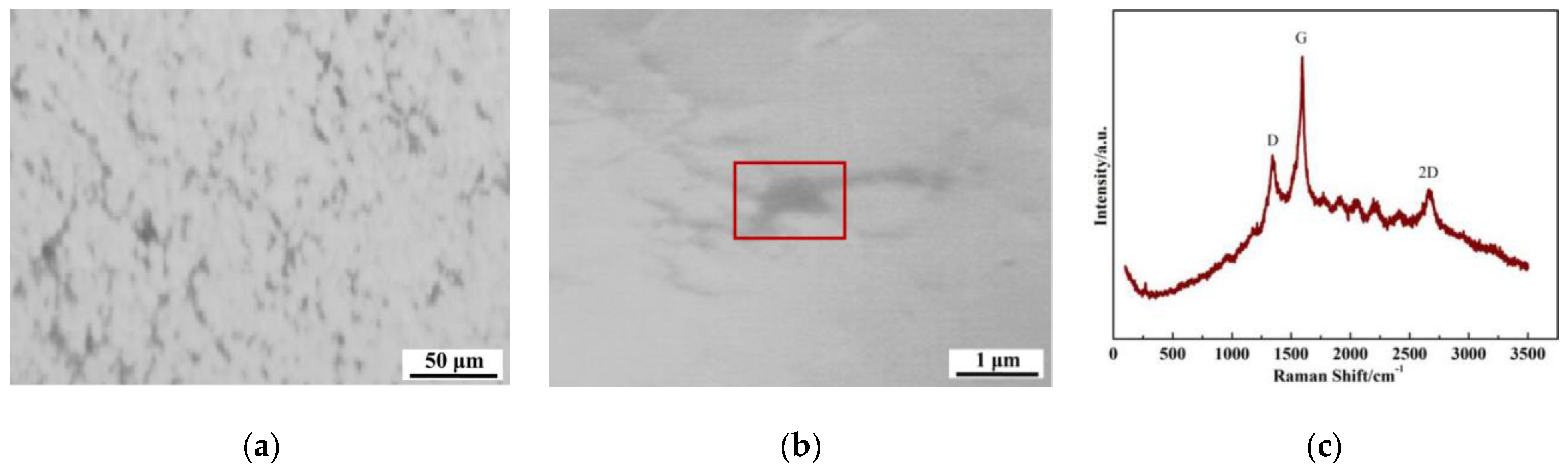
3.1. Microstructure and Morphology of Graphene-Enhanced CuW Composites

The microstructure and morphology of the graphene-enhanced CuW composites were meticulously examined using a combination of advanced techniques, included Scanning Electron Microscope (SEM) coupled with Energy Dispersive Spectroscopy (EDS), Scanning Kelvin Probe Force Microscopy (SKPFM), Electron Back Scatter Diffraction (EBSD), and Raman Spectroscopy. These methods were utilized to confirm the existence of graphene in composites and characterize the composition and microstructure of graphene-enhanced CuW composites.
The SEM micrographs of both the ordinary CuW composites and the graphene-enhanced CuW composites are presented in Figure 2. It is evident from the field emission SEM images that a high-sensitivity white graphene phase is clearly distinguishable between the dark copper phase and the light gray tungsten phase. Notably, the grain size of graphene is finer than that of copper and tungsten. During the vacuum infiltration process, due to the infiltration flow of copper, graphene primarily resides in the microstructural defects and grain boundaries of copper and tungsten. This helps to fill the interfacial gaps and compensate for microstructural imperfections.
The microstructure and compositional distribution of graphene-enhanced CuW composites were further analyzed using EDS mapping. As depicted in Figure 3, the distribution of tungsten, copper, and carbon within these composites was clearly observed. Notably, the copper phase is seen infiltrating and filling the voids within the tungsten skeleton phase. Additionally, the EDS mapping of the carbon element revealed that graphene is uniformly dispersed throughout the tungsten phase, with some noticeable aggregation observed at the phase interface between tungsten and copper.
SKPFM is a characterizing technique which applies scanning Kelvin probe on the basis of atomic force microscopy (AFM). This method simultaneously enables nanometer-scale topography measurement and high-resolution in situ Volta potential mapping. Due to the disparities in electronic work functions among carbon, copper, and tungsten, the distribution of low-potential tungsten and high-potential copper phases can be preliminarily distinguished using SKPFM.
By integrating the EDS mapping results presented in Figure 3 with AFM height scanning and SKPFM surface potential scanning, an in situ characterization of the surface height and potential of graphene-enhanced CuW composites is conducted. As depicted in Figure 4, as the distance varies, the surface potential undergoes changes within the range of 0 to 10 μm. Notably, the surface height exhibits significant and synchronous variations with the potential at approximately 6 μm. This correlation further corroborates that the predominant phase at the boundary between tungsten and copper is carbon-based.
EBSD can be used to analyze the microstructure and orientation of solid crystal materials under different process conditions. In order to study the texture and orientation of graphene-enhanced CuW composites, the sample was analyzed using a Thermo Scientific Helios 5 UX focused ion beam electron microscopy. The texture of face-centered cubic metal includes {011}<100> goss texture, (112)<111> copper texture, {111}<211> R texture, {001}<100> cubic texture, and {011}<211> brass texture. Copper is a face-centered cubic crystal. In the experiment, the crystal orientation of <001>, <101>, and <111> is represented as a triangle. EBSD results of element distribution mapping and grain orientation diagram of CuW composites and graphene-enhanced CuW composites are shown in Figure 5. From the element distribution maps in Figure 5a,c, it can be seen that the distribution of Cu in CuW80 forms a nearly three-dimensional network structure which is relatively uniform and continuous, with only a small number of areas experiencing concentration and aggregation. However, the connection between some W is not dense enough, making the network-like Cu veins clearly visible, indicating that the metallurgical bonding degree between W–W is still insufficient. After sintering, there are still a few pores inside the material, which also makes the distribution of some Cu too concentrated. In the CuW80 alloy modified with graphene, the W–W bond becomes tighter, and Cu is uniformly distributed in small and uniform gaps, which also reduces the phenomenon of Cu phase segregation. C particles are mostly distributed at the boundary of W, and are often enveloped by Cu.
There are three main colors in the orientation map, and different colors represent the different orientations of grains. Figure 5b shows the EBSD orientation map of CuW80 material. It can be seen that the grains are mostly concentrated in the <101> orientation, and the proportion of grains with <001> and <111> orientations is relatively small. The distribution of grains with different orientations is relatively dispersed. The number of <101>-oriented grains in the CuW80 material modified with a small amount of graphene is significantly reduced, and the distribution of grains with different orientations is also more dispersed. At the same time, orientation changes also occurred on multiple identical grains. In summary, after adding graphene, the element distribution of CuW80 material becomes more compact and uniform, and the grain orientation undergoes significant changes.
The microstructure of graphene-enhanced CuW composites was analyzed using Raman spectroscopy, as shown in Figure 6. Upon analyzing the Raman spectrum curve at the designated location, it was observed that the peak position coincided significantly with the characteristic peak of graphene, verifying the existence of a graphene structure within that area. The sharp G peak at 1580 cm−1 represents the carbon of sp2 hybrid structure, which proves the existence of graphene, while the D peak at 1350 cm−1 represents the carbon of a sp3 hybrid structure, and indicates that a certain defect structure exist. The ratio of 2D peak to G peak can be used to determine that the graphene here is not a monolayer structure, but a certain multilayer graphene aggregation structure [34]. In summary, it can be proved that graphene exists in CuW composites, and it should exist at the interface between copper and tungsten to fill gaps and make up for defects.
The X-ray Diffraction technique is mainly used to identify the phase of the material based on cell dimension units. Figure 7 shows X-ray diffraction (XRD) results of CuW composites and graphene-enhanced CuW composites, respectively. The sample without adding graphene mainly shows tungsten and copper diffraction peaks at 2θ values of ~40.264 (110), ~58.274 (200), ~73.195 (211), ~43.297 (111), and ~50.433 (200). While in the XRD patterns of graphene-enhanced CuW composites, minor WC phases can be identified, i.e., the weak peaks emerged at 2θ equal to 31.511 (001), 35.641 (100), and 48.296 (101), respectively. This indicates that during the prolonged high-temperature vacuum infiltration sintering process, a very small amount of graphene may react with tungsten to form tungsten–carbon compounds. Carbon atoms of graphene may diffuse onto the surfaces of the W–W skeletons and easily into the octahedral spacings of the tungsten atoms due to the differences of the atom diameters of tungsten and graphene.

3.2. Mechanical and Electrical Properties of Graphene-Enhanced CuW Electrical Contacts

The density, bending strength, electrical conductivity, hardness, and relative density of CuW and graphene-enhanced CuW electrical contacts materials were measured and calculated. The resulting data and the corresponding standard deviation are summarized in Table 1.
As shown in Table 1, the bending strength and hardness of CuW electrical contacts materials without graphene are 1058 MPa and 234 HB. With the doping reinforcement of graphene, the mechanical properties increased significantly, and the bending strength and hardness increased to 1160 MPa and 248 HB, respectively. The occurrence of this phenomenon can be attributed to the improvement of the size of tungsten particles in the composites by graphene. The higher the graphene content, the smaller the size of tungsten particles in the system; therefore, the hardness increases. From the micro-morphology, the fine tungsten particles are dispersed in copper, which strengthens the weaker copper phase indirectly and is resisted by fine tungsten particles in the process of deformation; therefore, the hardness is improved.
From the data of electrical conductivity, it can be seen that the addition of graphene also have an effect on the electrical conductivity of CuW electrical contacts materials. Different from traditional reinforcing additive, the addition of graphene significantly improved the electrical conductivity of CuW electrical contacts materials, which increased from 38%IACS to 46.1%IACS. This is because graphene itself has higher electrical conductivity than copper, and also the graphene phase mainly exists at the microstructure defect and the grain boundary of copper and tungsten to construct a new continuous high conductivity network, which improves the electrical conductivity of materials.
In summary, graphene-reinforcement plays a key role in the synergistic improvement of mechanical and electrical properties of CuW composites. As the density is close, after adding graphene, the bending strength, hardness, and electrical conductivity of CuW composites increase by about 10%, 6%, and 20%, respectively.

3.3. Ablation Resistance of Graphene-Enhanced CuW Electrical Contacts

The innovative graphene-enhanced CuW electrical contacts have been integrated into the 252 kV/63 kA high-voltage SF6 circuit breaker, demonstrating an impressive 20 times effective full-capacity of continuous breaking in electrical durability tests, compared to the ordinary CuW electrical contacts which only achieved 16 times. As evident from Figure 8 and Table 2, the ablation degree of the graphene-enhanced CuW80 electrical contacts remains significantly lower even after 20 consecutive full-capacity 63 kA short-circuit current breakings, compared to the ordinary CuW80 contacts after just 16 breakings. Furthermore, the dimensional changes observed in both the stationary and movable contacts following full-capacity breaking are notably smaller in the graphene-enhanced CuW80 electrical contacts compared to their non-graphene counterparts.
The mechanisms underlying the significant improvement in the ablation resistance of CuW electrical contacts by the integration of graphene are intricate and multifaceted. The unique properties of graphene play a pivotal role in enhancing the durability and performance of electrical contacts. Firstly, the pinning effect induced by graphene during ablation is a crucial mechanism. This pinning effect hinders the flow of copper within the contact material, effectively mitigating the volatilization and enrichment of copper in the molten pool that occurs during the ablation process. By limiting the copper loss, the mass loss of the electrical contacts is significantly reduced, thereby enhancing their durability. Secondly, the exceptional electrical and thermal conductivity of graphene play a vital role. Graphene’s ability to quickly guide the heat generated by the arc ensures that the heat is efficiently dissipated, contributing to a shorter arc duration time. This reduction in arc duration not only minimizes the thermal stress on the contacts, but also significantly reduces the mass ablation that occurs during the arc event. Furthermore, the low work function of graphene promotes arc breakdown preferentially on the graphene phase. This preferential breakdown not only disperses the breakdown energy, but also promotes the dispersion of the arc, ensuring that the arc energy is distributed more uniformly across the contact surface. This dispersion of the arc energy reduces the concentration of heat at specific points, minimizing the loss of copper in the ablation center and further enhancing the durability of the electrical contacts.
In summary, the combination of the pinning effect, exceptional electrical and thermal conductivity, and preferential arc breakdown on the graphene phase collectively leads to substantial enhancements in the ablation resistance of CuW electrical contacts. These advancements not only bolster the durability of the electrical contacts, but also facilitate more efficient and dependable operation of the high-voltage circuit breakers in which they are employed.
Based on previous literature comparisons, it is evident that the properties of CuW composites vary with changes in their compositional content. Higher copper content offers superior electrical and thermal conductivity, whereas increased tungsten content enhances mechanical properties and ablation resistance. However, these two aspects cannot be fully optimized simultaneously, as an increase in one often leads to a decrease in the other [18]. By the third component doping modification, the enhancement of certain properties in composite materials is achievable, but it often results in a decrease in electrical conductivity, making it difficult to achieve a balance between the two [18,19,20,21,22].
Graphene, with its exceptional properties, can effectively enhance the overall performance of CuW composites when used as an additive. However, previous research on graphene-modified CuW composites has primarily focused on simulations, material microstructure characterization, and electrical ablation performance evaluation of samples. Although the superiority of graphene addition has been demonstrated from the perspective of material properties and ablation resistance, successful preparation of graphene–CuW electrical contact products has not been achieved. Furthermore, no studies have been conducted on the performance of graphene-enhanced CuW electrical contacts under actual interruption conditions in circuit breakers, lacking the guiding significance in actual use [18,28,29,30]. In this study, graphene-enhanced CuW80 composites and electrical contacts have been successfully prepared for the first time. Through circuit breaker type testing, the graphene-enhanced CuW80 electrical contacts were breaking 20 times under extreme short-circuit current conditions (peak voltage of 392 kV, current of 65 kA, and cumulative arc duration of 292.5 ms), demonstrating an improvement in their ablation resistance. This achievement holds significant importance in practical applications.

4. Conclusions

In this study, innovative CuW composites enhanced with graphene were prepared for use in high-voltage circuit breaker electrical contacts, employing an integrated vacuum infiltration technology. When compared to conventional CuW composites, the addition of graphene notably enhanced the comprehensive mechanical and electrical properties of the materials. Graphene primarily resided within the microstructure defects and grain boundaries of copper and tungsten, effectively filling interfacial gaps and compensating for microstructural imperfections. As a result of this reinforcement, the bending strength, hardness, and electrical conductivity of the CuW composites increased by approximately 10%, 6%, and 20%, respectively.
The innovative graphene-enhanced CuW electrical contacts exhibited superior ablation resistance, making them suitable for application in a 252 kV/63 kA high-voltage SF6 circuit breaker. These innovative electrical contacts successfully achieved 20 times effective consecutive full-capacity short-circuit current breaking events during electrical durability testing. It opens a new avenue for the development and application of high-performance graphene-enhanced CuW electrical contacts. Furthermore, it is anticipated that these innovative contacts will find widespread application in high-voltage circuit breakers of even higher voltage grades in the future.

5. Prospects

The electrical contact, serving as the core of the high-voltage circuit breaker, is a crucial factor influencing its breaking capacity. As the increasingly serious problem of over-standard short-circuit currents, circuit breakers are evolving towards higher voltage ratings and larger breaking capacities. Additionally, electrical contacts used in reactive power compensation circuit breakers and filter group circuit breakers must adapt to frequent switching conditions, necessitating enhanced resistance to arc erosion and mechanical wear. Traditional copper–tungsten alloy materials are gradually becoming inadequate in meeting these demands.
Graphene-enhanced electrical contact technology, utilizing graphene’s high strength, conductivity, and thermal conductivity, is expected to significantly reduce the failure rate of high-capacity circuit breakers, mitigating the problem of over-standard short-circuit currents. This holds significant importance in ensuring the safe, stable, and reliable operation of high-voltage transmission system, and it will drive advancements and innovations in electrical contact materials for high-voltage circuit breakers.
Moreover, with the increasing demand for low-carbon, clean, and environmentally friendly technologies, high-voltage circuit breakers are gradually shifting towards vacuum or SF6 alternative gas medium environments. Therefore, there is an urgent need for further research on novel electrical contact materials suitable for these environmentally friendly atmospheres.

Author Contributions

Conceptualization, T.L., Y.H. and Y.D.; methodology, T.L., Z.P., D.J. and Y.F.; formal analysis, T.L., Z.P. and Y.F.; investigation, T.L., Z.P. and Y.F.; writing—original draft preparation, T.L. and D.J.; writing—review and editing, Y.F., Z.S., Y.H. and Y.D.; supervision, Z.S., Y.H. and Y.D.; funding acquisition, T.L., Z.P., Y.H. and Y.D. All authors have read and agreed to the published version of the manuscript.

Funding

This research was funded by the State Grid Corporation of China Science and Technology Foundation, grant number 5500-202158363A-0-0-00.

Institutional Review Board Statement

Not applicable.

Informed Consent Statement

Not applicable.

Data Availability Statement

The data presented in this study are shown in the paper.

Conflicts of Interest

Authors Dr. Tan Liu, Prof. Dr. Yu Han, Mr. Zhen Pang, and Prof. Dr. Yi Ding were employed by the company State Key Laboratory of Advanced Power Transmission Technology, State Grid Smart Grid Research Institute Co., Ltd. The remaining authors declare that the research was conducted in the absence of any commercial or financial relationships that could be construed as a potential conflict of interest.

References

  1. Wang, H.-T.; Wang, Z.-X.; Wang, L.-Z.; Wang, J.-Q.; Zhu, Y.-C. Effect of sintering temperature on the physical properties and electrical contact properties of doped AgSnO2 contact materials. Int. J. Miner. Metall. Mater. 2018, 25, 1275–1285. [Google Scholar] [CrossRef]
  2. Petrov, V.L.; Morozov, I.N.; Kuznetsov, N.M.; Soloviev, E.L. Investigation of High Voltage Circuit Breakers for Breaking Capacity Based on Simulation Models. In Power Electronics and High Voltage in Smart Grid: Select Proceedings of SGESC 2021; Springer: Singapore, 2022; pp. 173–182. [Google Scholar]
  3. Song, Y.; Wang, Z.; Zhang, H.; Li, M.; Liu, Y.; Yao, Y. Simulation Study on Electrical Life Breaking Capacity of 550kV SF6 Circuit Breaker. In Proceedings of the 2023 13th International Conference on Power and Energy Systems (ICPES), Chengdu, China, 8–10 December 2023; pp. 180–184. [Google Scholar]
  4. Lebedev, M.; Promakhov, V.; Schulz, N.; Vorozhtsov, A.; Lerner, M. Effects of Sintering Temperature on the Microstructure and Properties of a W-Cu Pseudo-Alloy. Metals 2023, 13, 1741. [Google Scholar] [CrossRef]
  5. Han, T.; Hou, C.; Sun, Y.; Li, Y.; Song, X. Effect of Grain Refinement on the Comprehensive Mechanical Performance of W–Cu Composites. Nanomaterials 2023, 13, 386. [Google Scholar] [CrossRef]
  6. Zou, J.; Song, D.; Shi, H.; Liang, S. Effects of grading tungsten powders on properties of CuW alloy. Mater. Res. Express 2020, 7, 26528. [Google Scholar] [CrossRef]
  7. Dong, L.L.; Ahangarkani, M.; Chen, W.G.; Zhang, Y.S. Recent Progress in Development of Tungsten-Copper Composites: Fabrication, Modification and Applications. Int. J. Refract. Met. Hard Mater. 2018, 75, 30–42. [Google Scholar] [CrossRef]
  8. Hamidi, A.G.; Arabi, H.; Rastegari, S. A Feasibility Study of W-Cu Composites Production by High Pressure Compression of Tungsten Powder. Int. J. Refract. Met. Hard Mater. 2011, 29, 123–127. [Google Scholar] [CrossRef]
  9. Wang, Q.; Ge, S.; Cao, W.; Yu, S.; Liao, Z. Study of Arc Interruption Characteristics under Rated Current in Low Voltage Circuit Breakers. Energies 2023, 16, 4114. [Google Scholar] [CrossRef]
  10. Wang, W.; Huang, Z.; Zhong, R.; Luo, Y.; Chen, S.; Yang, W.; Huang, J.; Zhao, S. Simulation of Arc Breaking in a 252kV Circuit Breaker under Harmonic Current. In Proceedings of the 2023 International Conference on Power System Technology (PowerCon), IEEE, Jinan, China, 21–22 September 2023; pp. 1–4. [Google Scholar]
  11. Sun, J.; Li, Z.; Wang, H.; Liu, J.; Lei, D.; Wang, X. Rebreakdown Characteristics of Vacuum Circuit Breaker in its Breaking Process under DC Voltage. In Proceedings of the 2023 IEEE 4th International Conference on Electrical Materials and Power Equipment (ICEMPE), Shanghai, China, 1–10 May 2023; pp. 1–4. [Google Scholar]
  12. Zhao, Z.; Guo, J.; Yu, F.; Rao, X.; Wu, X. Study on working condition of 750 kV AC filter breaker in  ±1100 kV UHVDC system. J. Eng. 2019, 2019, 839–844. [Google Scholar] [CrossRef]
  13. Shu, Y.; Chen, W. Research and application of UHV power transmission in China. High Volt. 2018, 3, 1–13. [Google Scholar] [CrossRef]
  14. Liu, Z.; Zhang, F.; Yu, J.; Gao, K.; Ma, W. Research on key technologies in ±1100 kV ultra-high voltage DC transmission. High Volt. 2018, 3, 279–288. [Google Scholar] [CrossRef]
  15. Yao, F.; Chen, W.; Yang, Y.; Zhou, K.; Li, R.; Elmarakbi, A.; Fu, R. Engineering performance of tungsten network reinforced copper matrix composites synthesized by selective laser melting and infiltration. Sci. Technol. Adv. Mater. 2024, 25, 2309888. [Google Scholar] [CrossRef] [PubMed]
  16. Yuan, J.; Liu, Y.; Zhu, T.; Yang, B.; Long, Y.; Yao, F.; Chen, D.; Tang, Z. Exploration of a micro multi-electrode technology applied in an air arc heater. J. Phys. D Appl. Phys. 2021, 54, 385205. [Google Scholar] [CrossRef]
  17. Ding, Y.; Geng, J.F.; Du, J.L.; Wei, S.H.; Zhu, Z.X.; Han, Y.; Xia, D.; Xie, W.; Chen, X.; Ma, F.Y. High anti-arc erosion performance of the Al2O3 reinforced Cu@W composites for high voltage circuit-breaker contacts. Mater. Res. Express 2022, 9, 36504. [Google Scholar] [CrossRef]
  18. Duan, J.; Guo, X.; Huang, T.; Song, K.; Feng, J.; Wang, X.; Zhong, J.; Duan, K.; Zhang, Y. Arc ablation resistance behavior of Cu-W alloys with different W contents under atmospheric environment. Mater. Today Commun. 2023, 34, 105173. [Google Scholar] [CrossRef]
  19. Li, J.; Fang, F.; Wang, Z.; Zhang, G.; Wei, S.; Xu, L.; Pan, K. Microstructure and properties characterization of W-25Cu composite materials liquid-liquid doped with La2O3. Int. J. Refract. Met. Hard Mater. 2018, 71, 115–121. [Google Scholar] [CrossRef]
  20. Luo, L.-M.; Lu, Z.-L.; Huang, X.-M.; Tan, X.-Y.; Luo, G.-N.; Cheng, J.-G.; Zan, X.; Zhu, X.-Y.; Wu, Y.-C. Fabrication of W–Cu/La2O3 composite powder with a novel pretreatment prepared by electroless plating and its sintering characterization. Int. J. Refract. Met. Hard Mater. 2015, 48, 1–4. [Google Scholar] [CrossRef]
  21. Yang, X.; Liang, S.; Wang, X.; Xiao, P.; Fan, Z. Effect of WC and CeO2 on microstructure and properties of W–Cu electrical contact material. Int. J. Refract. Met. Hard Mater. 2010, 28, 305–311. [Google Scholar] [CrossRef]
  22. Mu, Z.; Geng, H.-R.; Li, M.-M.; Nie, G.-L.; Leng, J.-F. Effects of Y2O3 on the property of copper based contact materials. Compos. Part B Eng. 2013, 52, 51–55. [Google Scholar] [CrossRef]
  23. Mbayachi, V.B.; Ndayiragije, E.; Sammani, T.; Taj, S.; Mbuta, E.R.; Khan, A.U. Graphene synthesis, characterization and its applications: A review. Results Chem. 2021, 3, 100163. [Google Scholar] [CrossRef]
  24. Tomanik, E.; Christinelli, W.; Souza, R.M.; Oliveira, V.L.; Ferreira, F.; Zhmud, B. Review of Graphene-Based Materials for Tribological Engineering Applications. Eng 2023, 4, 2764–2811. [Google Scholar] [CrossRef]
  25. Zhang, L.; Ye, Q.; Zeng, X.; Liu, S.; Chen, H.; Tao, Y.; Yu, X.; Wang, X. Preparation and Properties of Graphene Reinforced Copper Electrical Contact Materials for High-Voltage Direct Current Electrical Contacts. Electronics 2023, 13, 53. [Google Scholar] [CrossRef]
  26. Naser, S.a.E.; Badmus, K.O.; Khotseng, L. Synthesis, Properties, and Applications of Metal Organic Frameworks Supported on Graphene Oxide. Coatings 2023, 13, 1456. [Google Scholar] [CrossRef]
  27. Wang, J.; Hu, D.; Zhu, Y.; Guo, P. Electrical Properties of In Situ Synthesized Ag-Graphene/Ni Composites. Materials 2022, 15, 6423. [Google Scholar] [CrossRef]
  28. Xu, R.; Zhou, M.; Wang, X.; Matharage, S.Y.; Yan, J.D.; Connolly, A.; Luo, Y.; Ding, Y.; Wang, Z. A molecular dynamics simulation study on the role of graphene in enhancing the arc erosion resistance of Cu metal matrix. Comput. Mater. Sci. 2022, 212, 11549. [Google Scholar] [CrossRef]
  29. Lin, F.; Xu, R.; Zhou, M.; Young, R.J.; Kinloch, I.A.; Ding, Y. Mechanical and Electrical Properties of Graphene Oxide Reinforced Copper–Tungsten Composites Produced via Ball Milling of Metal Flakes. Materials 2022, 15, 7736. [Google Scholar] [CrossRef]
  30. Ding, Y.; Liu, B.; Li, M.; Hao, L.; Zhu, Z.; Han, Y.; Ma, F.; Xiang, Z. High performance copper-tungsten@ graphene composites materials. J. Phys. Conf. Series. IOP Publ. 2022, 2321, 12010. [Google Scholar] [CrossRef]
  31. Gonzales, A.J.; Philofsky, E.M. Applications of scanning electron microscopy to thin film studies on semiconductor devices. Proc. IEEE 1971, 59, 1429–1433. [Google Scholar] [CrossRef]
  32. Zhang, B.; Zhu, Q.; Xu, C.; Li, C.; Ma, Y.; Ma, Z.; Liu, S.; Shao, R.; Xu, Y.; Jiang, B.; et al. Atomic-scale insights on hydrogen trapping and exclusion at incoherent interfaces of nanoprecipitates in martensitic steels. Nat. Commun. 2022, 13, 3858. [Google Scholar] [CrossRef] [PubMed]
  33. Bumbrah, G.S.; Sharma, R.M. Raman spectroscopy-Basic principle, instrumentation and selected applications for the characterization of drugs of abuse. Egypt. J. Forensic Sci. 2016, 6, 209–215. [Google Scholar] [CrossRef]
  34. Li, X.; An, M.; Li, P.; Miu, J.; Wu, Q.; Zheng, F.; Jiang, J.; Wang, H.; Huang, Y.; Li, Q. Phenylamine-Functionalized Graphene-Copper Composites with High Thermal Conductivity: Implications for Thermal Dissipation. ACS Appl. Nano Mater. 2021, 4, 12170–12179. [Google Scholar] [CrossRef]
Figure 1. The preparation process of graphene-enhanced CuW composites and electrical contacts.
Applsci 14 02731 g001
Figure 2. The SEM micrographs of CuW composites and graphene-enhanced CuW composites. (a,b) CuW80; (c,d) graphene-enhanced CuW80.
Applsci 14 02731 g002aApplsci 14 02731 g002b
Figure 3. The SEM-EDS micrographs of graphene-enhanced CuW composites. (a) Optical image; (b) EDS mapping of tungsten element; (c) EDS mapping of copper element; (d) EDS mapping of carbon element.
Applsci 14 02731 g003
Figure 4. In situ characterization of AFM height scanning and SKPFM surface potential scanning. (a,b) AFM and SKPFM images of graphene-enhanced CuW composites; (c) trend chart of height changing with distance; (d) trend chart of potential changing with distance.
Applsci 14 02731 g004
Figure 5. EBSD characterization of CuW composites and graphene-enhanced CuW composites. (a) Element distribution mapping of CuW80; (b) grain orientation diagram of CuW80; (c) element distribution mapping of graphene-enhanced CuW80; (d) grain orientation diagram of graphene-enhanced CuW80.
Applsci 14 02731 g005
Figure 6. Raman characterization of graphene-enhanced CuW composites. (a) Raman spectroscopy image; (b) the position of the Raman spectrum sampling point; (c) Raman spectrum of graphene-enhanced CuW composites.
Applsci 14 02731 g006
Figure 7. XRD patterns of CuW composites and graphene-enhanced CuW composites.
Applsci 14 02731 g007
Figure 8. Ablation images of electrical contacts after full-capacity breaking. (a) CuW80; (b) graphene-enhanced CuW80.
Applsci 14 02731 g008
Table 1. Mechanical and electrical properties of graphene-enhanced CuW composites and ordinary CuW composites.
CuW80SDGr-CuW80SD
Density (g/cm3)15.470.0615.490.03
Bending strength (MPa)10585.6611606.48
Electrical conductivity (%IACS)381.4146.10.51
Hardness (HB)2344.322483.74
Relative density (%)98/99.38/
Table 2. Size changes of graphene-enhanced CuW80 electrical contacts and ordinary CuW80 electrical contacts before and after ablation.
ComponentTest ItemSize Changes before and after Ablation
CuW80Gr-CuW80
Stationary arc contactEnd diameter of contact0.330.46
Contact length−7.24−9.57
Moveable arc contactExternal diameter of contacts−1.63−1.83
Internal diameter of contacts−1.4−1.64
Thickness of contacts0.170.17
Contact height−3.2−4.5
Disclaimer/Publisher’s Note: The statements, opinions and data contained in all publications are solely those of the individual author(s) and contributor(s) and not of MDPI and/or the editor(s). MDPI and/or the editor(s) disclaim responsibility for any injury to people or property resulting from any ideas, methods, instructions or products referred to in the content.

