Article

Enhancing the Photocatalytic Activity of Immobilized TiO2 Using Laser-Micropatterned Surfaces

by
Theodoros Giannakis
1,2,
Sevasti-Kiriaki Zervou
3,
Theodoros M. Triantis
3,
Christophoros Christophoridis
3,4,*,
Erasmia Bizani
4,5,
Sergey V. Starinskiy
1,
Panagiota Koralli
1,
Georgios Mousdis
1,
Anastasia Hiskia
3 and
Maria Kandyla
1,*
1
Theoretical and Physical Chemistry Institute, National Hellenic Research Foundation, 48 Vasileos Constantinou Avenue, 11635 Athens, Greece
2
Department of Physics, National and Kapodistrian University of Athens, University Campus, Zografou, 15784 Athens, Greece
3
Photo-Catalytic Processes and Environmental Chemistry Laboratory, Institute of Nanoscience and Nanotechnology, NCSR DEMOKRITOS, Neapoleos 27, Agia Paraskevi, 15341 Athens, Greece
4
Greener Than Green Technologies S.A., 13 Ilission St., Kifisia, 14564 Athens, Greece
5
Analytical Chemistry Laboratory, Chemistry Department, National and Kapodistrian University, University Campus, Zografou, 15784 Athens, Greece
*
Authors to whom correspondence should be addressed.
Appl. Sci. 2024, 14(7), 3033; https://doi.org/10.3390/app14073033
Submission received: 30 December 2023 / Revised: 24 March 2024 / Accepted: 26 March 2024 / Published: 4 April 2024

Abstract

:
In the past, the application of TiO2 slurry reactors has faced difficulties concerning the recovery and reusability of the catalyst. In response to these challenges, immobilized photocatalyst systems have been investigated, wherein the catalyst is fixed onto a solid support, frequently with reduced photocatalytic performance. In the present study, thin TiO2 films were developed in the anatase phase by the sol-gel process and spin-cast on laser-microstructured silicon substrates, to form photocatalytic surfaces of increased activity. The TiO2 films were thoroughly characterized using SEM-EDX, XRD, UV–Vis spectroscopy, and Raman spectroscopy. The photocatalytic activity of these surfaces was evaluated by the degradation of atrazine in aqueous solution under UV irradiation. Their photocatalytic activity was found to be significantly enhanced (mean kobs 24.1 × 10⁻³ min−1) when they are deposited on laser-microstructured silicon compared with flat silicon (mean kobs 4.9 × 10⁻³ min−1), approaching the photocatalytic activity of sol-gel TiO2 fortified with Degussa P25, used as a reference material (mean kobs 32.7 × 10⁻³ min−1). During the photocatalytic process, several transformation products (TPs) of atrazine, namely 2-chloro-4-(isopropylamino)-6-amino-s-triazine (CIAT), 2-chloro-4-amino-6-(ethylamino)-s-triazine (CAET), and 2-chloro-4.6-diamino-s-triazine (CAAT), were identified with LC–MS/MS. The stability of the photocatalytic surfaces was also investigated and remained unchanged through multiple cycles of usage. The surfaces were further tested with two other pollutants, i.e., 2,4,6-trichlorophenol and bisphenol-a, showing similar photocatalytic activity as with atrazine.

1. Introduction

Photocatalysis is a promising and environmentally friendly process that utilizes semiconductor materials to drive chemical reactions under the influence of light. The process involves the generation of electron–hole pairs upon exposure to light, initiating redox reactions that can decompose pollutants or facilitate other desirable transformations [1]. Photocatalysis offers an attractive alternative to conventional water treatment technologies, leading directly to the degradation of organic pollutants, compared to transferring them from one phase to another as in the case of membranes or activated carbon. The most commonly studied photocatalyst is titanium dioxide (TiO2) due to its excellent stability, non-toxicity, and enhanced photocatalytic activity [2,3].
However, the implementation of TiO2 slurry reactors has encountered challenges related to catalyst recovery and reusability. In traditional slurry systems, the photocatalyst is suspended in a liquid, rendering separation and filtration processes cumbersome and energy intensive. The use of TiO2 slurry reactors often leads to difficulties in maintaining a stable catalyst concentration and poses challenges in recovering the catalyst from the reaction mixture. This may result in increased costs and environmental concerns associated with the disposal of the slurry [4].
To address these issues, immobilized photocatalyst systems have been explored, where the catalyst is immobilized onto a solid support [5,6,7,8]. This approach not only simplifies catalyst recovery but also enhances the stability of the photocatalytic process [9,10].
Using immobilized photocatalysts allows for easy separation of the catalyst from the reaction medium, enabling its reuse and reducing the overall environmental impact. Moreover, the immobilization process can be tailored to specific substrates or matrices, providing flexibility in the design and application of photocatalytic systems [10,11]. Overall, the transition from TiO2 slurry reactors to immobilized photocatalyst systems represents a significant advancement in the field, addressing the challenges associated with catalyst recovery and contributing to the sustainable development of photocatalytic technologies [4,9].
Various chemical and physical techniques, such as chemical vapor deposition (CVD) [12], sol-gel [13], hydrothermal synthesis [14], metal organic chemical vapor deposition (MOCVD) [15], and pulsed laser deposition (PLD) [16], have been employed for the preparation of TiO2 thin films. The method of preparation significantly influences the properties of the films, with many processes requiring expensive infrastructure as well as high temperatures and pressures. Among these methods, the sol-gel process stands out as a common and advantageous approach for producing thin solid films and coatings on diverse substrates, offering benefits such as low cost, simplicity, low process temperatures, homogeneity control, and potential for large-scale production. Additionally, the sol-gel process enables the customization of material properties through the control of synthetic conditions [17].
While thin TiO2 films have been employed previously as photocatalysts for water contaminant removal [18], their photocatalytic behavior is limited by a low specific surface area, resulting from agglomerations in their micro/nanostructure and random orientation. To address this limitation, numerous efforts have focused on increasing the surface area of TiO2 films, often achieved through porosity control [19,20,21]. Various methods, including atomic layer deposition [22], sol-gel synthesis [23], hydrothermal reaction [24], and 3D printing [25], have been employed to tailor the porosity of TiO2. Additionally, increasing its specific area has been pursued through the development of needle-like microstructures [26,27] and the fabrication of aligned TiO2 nanotubes [28,29], among others.
A complementary approach to achieve a large surface area consists of combining a thin film with a patterned substrate, which offers a 3D morphology. Silicon is often used for this purpose due to its abundance and extended variety of patterning techniques available. In the field of micro/nanopatterning silicon surfaces, laser structuring methods have been often implemented [30,31]. Different wavelengths and pulse durations, such as 248 nm (nanosecond excimer) [32,33], 800 nm (femtosecond Ti:Sapphire) [34,35], 355/532 nm (nanosecond Nd:YAG lasers) [36,37], etc., have been employed to create specific morphologies on silicon, while the influence of ambient media, including vacuum, water, sulfur hexafluoride (SF6), ethanol, and others, has been thoroughly investigated [30,38,39]. Micro/nanostructured silicon, owing to its high absorption across a wide electromagnetic spectrum, finds diverse applications, such as solar cell and photodetector development, surface-enhanced Raman spectroscopy, and others [38]. The wettability/biomimetic [40,41,42] and cell growth properties [43] of micro/nanostructured silicon substrates have been extensively explored due to their unique morphology. Similarly, the large surface area of micro/nanostructured silicon makes it an attractive substrate for enhancing the photocatalytic activity of immobilized coatings.
Since there is an increasing interest in using photocatalysis for water treatment, a reliable evaluation of catalytic material performance is necessary. The European Committee for Standardization, CEN TC386/WG3, has developed a standard for the assessment of the photocatalytic activity of bulk materials [44]. Evaluating photocatalytic material performance in water purification relies on measuring phenol degradation under controlled conditions with UV irradiation. However, it is important to note that this assessment cannot be extrapolated to photocatalytic surfaces. Two ISO standards, ISO 10678:2010 and ISO 10676:2010, are available for assessing the photocatalytic activity of surfaces concerning water purification, which are based on the photobleaching of methylene blue and the oxidation of dimethyl sulfoxide (DMSO), respectively [45,46]. While these standards focus on assessing photocatalytic surfaces, they exhibit reliability shortcomings. In ISO 10676:2010, methylene blue assesses the photocatalytic activity of a surface; however, its photobleaching, influenced by photosensitization, may contribute significantly to the observed dye decomposition [47]. In ISO 10676:2010, DMSO is an unconventional test pollutant for photocatalysis, lacking recognition and extensive study compared to well-established pollutants like chlorophenols and pesticides. Furthermore, the use of this standard, requiring both ion and gas chromatography, adds complexity to its experimental implementation [47]. Consequently, the aforementioned ISO standards may not always be well-suited for their intended purposes. Conversely, the photocatalytic degradation of atrazine has undergone thorough investigation with various photocatalysts, rendering it a fitting substrate for appraising the photocatalytic efficacy of both bulk materials and surfaces. Moreover, its stability under UV light and low detection limit enable the photocatalytic assessment of surfaces with modest dimensions [48].
While microstructured silicon has been previously employed as a photocatalytic substrate with zinc oxide (ZnO) as the active material [49], the present study investigates the activity of the more commonly employed TiO2 photocatalyst, combined with microstructured silicon substrates with increased surface area.
The objectives of this study are (a) to develop and characterize novel thin TiO2 films by the sol-gel process, (b) to spin-cast these films on laser-microstructured silicon substrates to form the photocatalytic surfaces, (c) to evaluate their photocatalytic activity against a selected organic pollutant (atrazine) in aqueous solutions under UV irradiation, and d) to investigate the stability of the photocatalytic surfaces through multiple cycles of usage. Furthermore, the photocatalytic activity of TiO2 films on laser-microstructured silicon is evaluated against two other pollutants, i.e., 2,4,6-trichlorophenol and Bisphenol-a, to explore the application range of these surfaces. To the best of our knowledge, this is the first study that improves the photocatalytic efficiency of the traditional TiO2 photocatalyst by combining it with novel patterned substrates. The resulting immobilized photocatalytic surfaces present the advantage that no filtration is required after water treatment to remove residues of the photocatalyst, which significantly reduces the cost of the process. All fabrication methods employed in this work (sol-gel synthesis and laser structuring) are amenable to scale up for the development of high-volume and low-cost photocatalytic reactors for water purification.
This comprehensive investigation seeks to contribute valuable insights into the relationship between surface morphology and photocatalytic efficiency, offering a nuanced understanding that can inform the design and development of highly efficient TiO2-based photocatalysts for environmental remediation and energy applications.

2. Materials and Methods

2.1. Standards and Reagents

Analytical standards of atrazine (purity 99.1%), bisphenol-a, and 2,4,6-trichlorophenol were purchased by Sigma-Aldrich (Seelze, Germany) and isotopic labeled atrazine-d5 standard solution was obtained from Dr. Ehrenstorfer GmbH (Augsburg, Germany). Acetonitrile (ACN) of LC-MS grade (≥99.9%) was supplied by Fisher Chemical. Ultra-pure water (18.2 MΩ cm at 25 °C) was produced in the lab using a Temak TSDW10 water purification system (TEMAK, Athens, Greece).
For the synthesis of TiO2 films, the following high-purity starting materials were used: titanium (IV) isopropoxide (TTIP; 98%, Acros Organics, Waltham, MA, USA), 2-methoxyethanol (C3H8O2; 99.8%, Acros Organics, Waltham, MA, USA), nitric acid (HNO3; 70%, Sigma–Aldrich), and commercial Degussa P25 (Degussa AG, Frankfurt, Germany).

2.2. Synthesis of Photocatalysts and Coating of Substrates

Thin TiO2 films were developed by the sol-gel process, followed by spin-coating on two distinct substrates: flat and microstructured silicon. Glass substrates were also used for UV–visible spectroscopy. Two precursor solutions, labeled A and B, were prepared. Solution A was formulated by dissolving 1 mL of TTIP in 5 mL of C3H8O2, while solution B was created by adding 0.15 mL of nitric acid to 0.25 mL of water. The final solution was prepared by carefully adding solution B drop by drop, under stirring, into solution A at 80 °C. The resultant solution underwent stirring at 80 °C for 2 h and was subsequently allowed to rest at room temperature (RT) for 1 day. The reference TiO2 solution, doped with Degussa P25, was prepared by introducing 50 mg of Degussa P25 into 1 mL of the aged TiO2 solution. Thin films were produced by depositing 6–7 droplets of the final solutions onto different substrates and spin-coating (Laurell WS-400BX-6NPP/LITE, Lansdale, PA, USA) at 1400 rpm for 30 s, followed by 400 rpm for an additional 30 s. This spin-coating procedure was repeated three times. Each spin-cast layer was subjected to heating at 100 °C on a hot plate for 5 min before applying the next layer. Finally, the films underwent thermal treatment at 500 °C for 3 h in a furnace (MUFFLE FURNACE N-8 L 1100 °C, JP Selecta, Barcelona, Spain) to achieve the desired crystalline structure [50]. The ramp rate during this thermal treatment was maintained at 2 °C min−1. Subsequently, all samples were allowed to cool down to RT.

2.3. Laser Microstructuring of Silicon Substrates

N-type silicon wafers with a (1 0 0) orientation were precisely cut into small dies (1.5 cm × 1.5 cm). Prior to laser microstructuring, a thorough cleaning process was employed to eliminate any residues from the sample surfaces. The wafers underwent ultrasonic bath treatment with acetone and methanol for 10 min each. The laser-structuring setup included a pulsed Q-switched Nd:YAG laser system, operating at a wavelength of 532 nm, with a pulse duration of 5 ns (FWHM), and a repetition rate of 10 Hz. The silicon samples were placed in a vacuum chamber, which underwent evacuation to a base pressure of 10−2 mbar before being filled with 600 mbar of SF6. A lens with a focal length of 20 cm was utilized to focus the laser beam onto the sample surface, achieving an incident fluence of ~1.1 J cm−2, which surpasses the threshold for monocrystalline silicon modification in the multi-pulse laser irradiation mode [38,51]. The distance between the lens and the sample surface was maintained at 16 cm. A computer-controlled set of x-y translation stages was used in order to raster-scan the sample relative to the laser beam for large-area patterning. The scanning speed was set to 62.5 μm s−1, resulting in each spot on the silicon surface receiving approximately 100 laser pulses during the irradiation process.

2.4. Characterization of Photocatalytic Surfaces

The structural, morphological, and optical properties of the photocatalytic materials underwent comprehensive characterization. X-ray diffraction (XRD) analysis was conducted using a Rigaku SmartLab instrument, employing Cu-Kα1 (λ = 1.540562 Å) and Cu-Kα2 radiation (λ = 1.54439 Å) at an intensity ratio of 2:1. Measurements were taken in the 2θ range of 20° to 80° with a step size of 0.03° and an exposure time of 3 s. Raman spectra were acquired using a Renishaw inVia Raman Microscope, employing backscattering geometry and a 2400 lines mm−1 diffraction grating. The experimental setup includes an argon-ion laser (514.5 nm) for excitation. All measurements were conducted with a ×50 magnification lens at RT, achieving a spectral resolution of 2 cm−1. For the determination of chemical composition and morphology, a Schottky field-emission ultra-high resolution scanning electron microscope (FE-SEM, JEOL F7610F, Tokyo, Japan) equipped with an energy-dispersive X-ray spectrometer (EDX), was utilized. The thickness of the TiO2 films deposited on flat silicon substrates was measured using a surface profilometer (Alpha Step IQ, KLA-Tencor, Milpitas, CA, USA). Furthermore, optical transmittance spectra were obtained on TiO2 films deposited on glass substrates at RT, across the spectral range of 300–800 nm, using a Perkin Elmer UV-vis-NIR Lambda 19 spectrophotometer with a scanning speed of 240 nm min−1.

2.5. Photocatalytic Device

Irradiation was performed with a laboratory-constructed “illumination box” (Figure S1), equipped with four F15W/T8 black light tubes (Sylvania GTE, Westfield, IN, USA) (Figure S1). The maximum emission of these tubes was around 365 nm, emitting 71.7 μW cm−2 at a distance of 25 cm.
Cells containing fortified atrazine solution in contact with under-investigation surfaces were used for photocatalysis experiments. Positioned at a distance of 11 cm from the light tubes, the cells were placed on a magnetic stirrer. Experiments were also performed using bisphenol-a and 2,4,6-trichlorophenol as test pollutants.

Selection of Photocatalytic Device Setup

To ensure a valid observation of the photocatalytic degradation of atrazine, a 2 mL volume of the fortified atrazine solution was selected. This volume was chosen to adequately cover the small photocatalytic surface area (1.5 cm × 1.5 cm). Simultaneously, an initial atrazine concentration of 30 μg L−1 (0.139 μmol L−1) was utilized, allowing for the measurement of changes in atrazine concentration during the photocatalytic process. The accuracy of measurements at this low concentration level was upheld by employing atrazine-d5 as an internal standard (IS).
In addition to tracking the decrease in atrazine concentration, the confirmation of its photocatalytic degradation involved monitoring the formation of photocatalytic transformation products (TPs), namely 2-chloro-4-(isopropylamino)-6-amino-s-triazine (CIAT), 2-chloro-4-amino-6-(ethylamino)-s-triazine (CAET), 2-chloro-4.6-diamino-s-triazine (CAAT), 2-hydroxy-4-(isopropylamino)-6-(ethylamino)-s-triazine (OIET), 2-hydroxy-4.6-diamino-s-triazine (OAAT), 2-hydroxy-4-hydroxy-6-amino-s-triazine (OOAT), and 2.4.6-thihydroxy-s-triazine (OOOT). These TPs are known to be generated during the photocatalysis of atrazine [48].
Moreover, the photocatalytic activity of the optimum surface (M-Si-solgel) was evaluated using bisphenol-a and 2,4,6-trichlorophenol solutions at a concentration of 30 μg L−1.

2.6. Photocatalytic Degradation Experiments

Photocatalysis experiments were performed in cylindrical pyrex cells (r = 2.5 cm and h = 4.5 cm), open on the upper side. Fortified aqueous solutions of atrazine (30 μg L−1) were prepared in water. A volume of 2 mL of the sample solution was added to the cells in each experiment in the presence and absence of the photocatalytic surfaces (1.5 cm × 1.5 cm) and it was left in the dark for 15 min before illumination to achieve equilibrium. Photolysis was performed at ambient temperature in the illumination box. The solutions were magnetically stirred throughout the experiment. UV light emission was interrupted at specific time intervals and samples (100 μL) were taken for LC-MS/MS analysis. The samples were spiked with atrazine-d5 (IS) at a final concentration of 30 μg L−1 (0.139 μmol L−1) and analyzed by LC-MS/MS.

Calculation of Kinetic Rate Constants

At several time intervals, samples were taken for analysis of atrazine by LC-MS/MS to obtain a plot of atrazine degradation over the time of irradiation. Sampling intervals covered the whole degradation process (e.g., from 10% to 90% degradation) unless the results indicated that no significant degradation of atrazine was observed or that degradation proceeded very slowly.
Experiments under irradiation, under dark, and under irradiation in the absence of the test surface were performed.
Observed degradation rate constants, kobs, were calculated by fitting the plots (natural logarithm (ln) of concentrations vs. reaction time) to a first-order kinetic model, as described by Equations (1) and (2) [3,52].
R a t e = d C d t = k o b s [ C ]
l n C = ln C 0 k o b s t
where the following definitions apply:
  • C0: initial concentration of atrazine (μmol L−1);
  • C: concentration of atrazine (μmol L−1);
  • t: reaction time (min);
  • kobs: observed rate constant (min−1).

2.7. Analytical Methods Used to Monitor Atrazine Degradation

The decay of the substrate and the production of intermediates were monitored using a TSQ Quantum Discovery Max triple-stage quadrupole mass spectrometer, coupled to a Finnigan Surveyor LC system, equipped with a Finnigan Surveyor AS autosampler (Thermo Electron Corporation, San Jose, PA, USA). The chromatographic column used for the separation of atrazine and TPs was an Atlantis T3 (2.1 mm × 100 mm, 3 μm, Waters, Wexford, Ireland) with isocratic elution. The mobile phase was composed of 40% acetonitrile–60% ultrapure water. The injection volume was 15 μL and the column temperature was set at 30 °C. Ionization of atrazine and its TPs was performed with an electron spray ionization (ESI) source in positive mode. Ionization of bisphenol-a and 2,4,6-trichlorophenol was performed with an atmospheric pressure chemical ionization (APCI) source in negative mode. The detection was performed in multiple reaction monitoring (MRM) mode. Table S1 lists the MRM transitions from precursors to product ions and the applied parameters that were used to monitor the decay of the compounds during the photocatalytic process. Xcalibur software 2.0 was used to control the MS parameters for data acquisition and data analysis.

3. Results and Discussion

In the frame of this study, five different surfaces were evaluated in terms of their photocatalytic efficiency: (a) Flat Si–TiO2 solgel (F-Si-solgel), (b) Flat Si–Degussa P25 + TiO2 solgel (F-Si-P25-solgel), (c) Microconical Si–TiO2 solgel (M-Si-solgel), (d) Microconical Si–Degussa P25 + TiO2 solgel (M-Si-P25-solgel), and (e) Rippled Si-TiO2 solgel (R-Si-solgel). The first two surfaces consist of flat silicon substrates coated either with the pure TiO2 film or with the composite TiO2 + Degussa P25 film. The latter is used as a reference coating, against which the photocatalytic activity of the materials developed in this work is assessed. Surfaces c and d consist of laser-patterned, microconical silicon substrates coated either with the pure TiO2 film or with the composite TiO2 + Degussa P25 film. The R-Si-solgel surface consists of laser-patterned, rippled silicon substrates, coated with the pure TiO2 film. The purpose of the two different patterned silicon substrates (microconical and rippled) is to evaluate the effect of the substrate morphology on the photocatalytic activity of the surface.

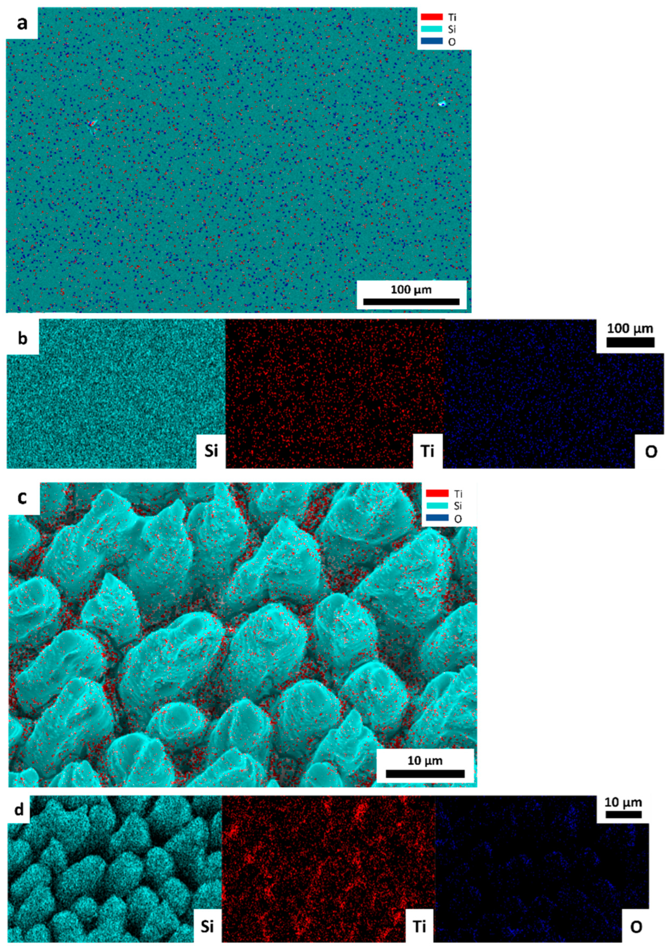
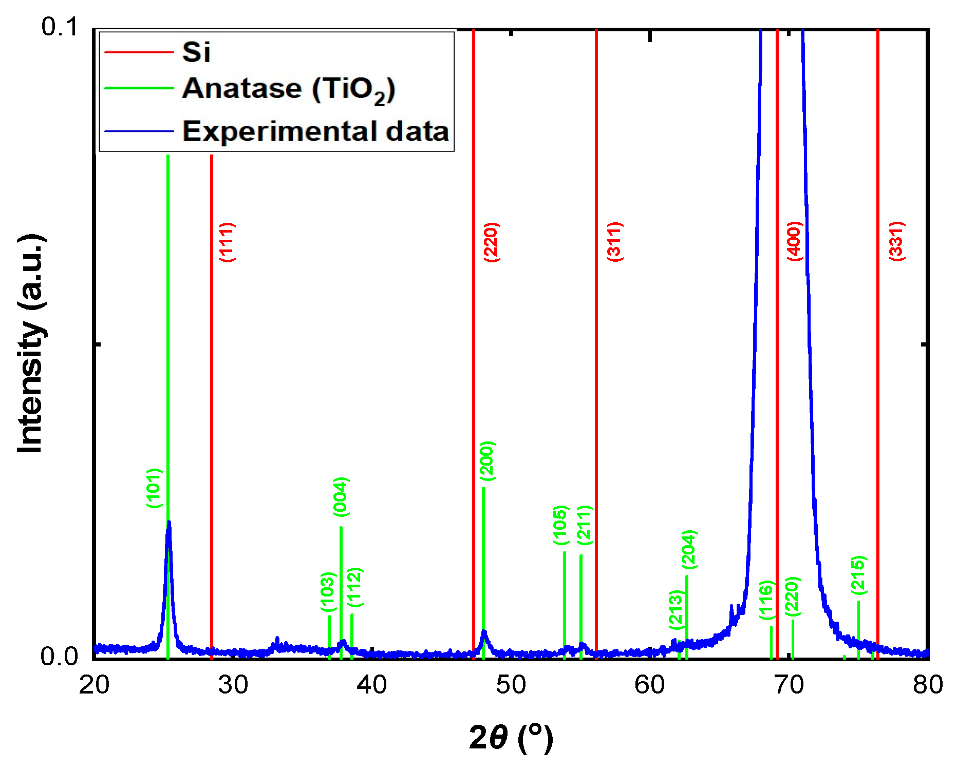
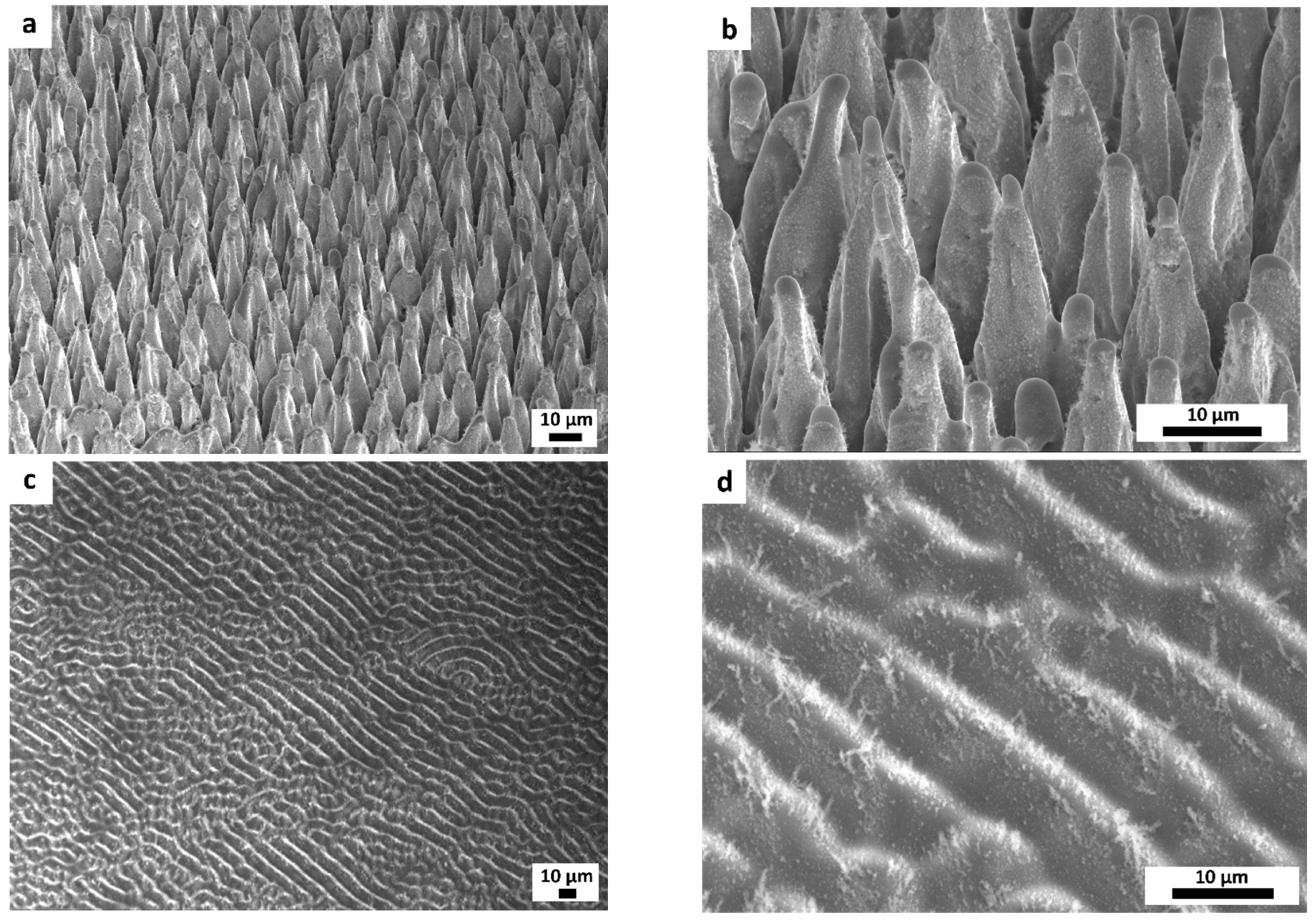
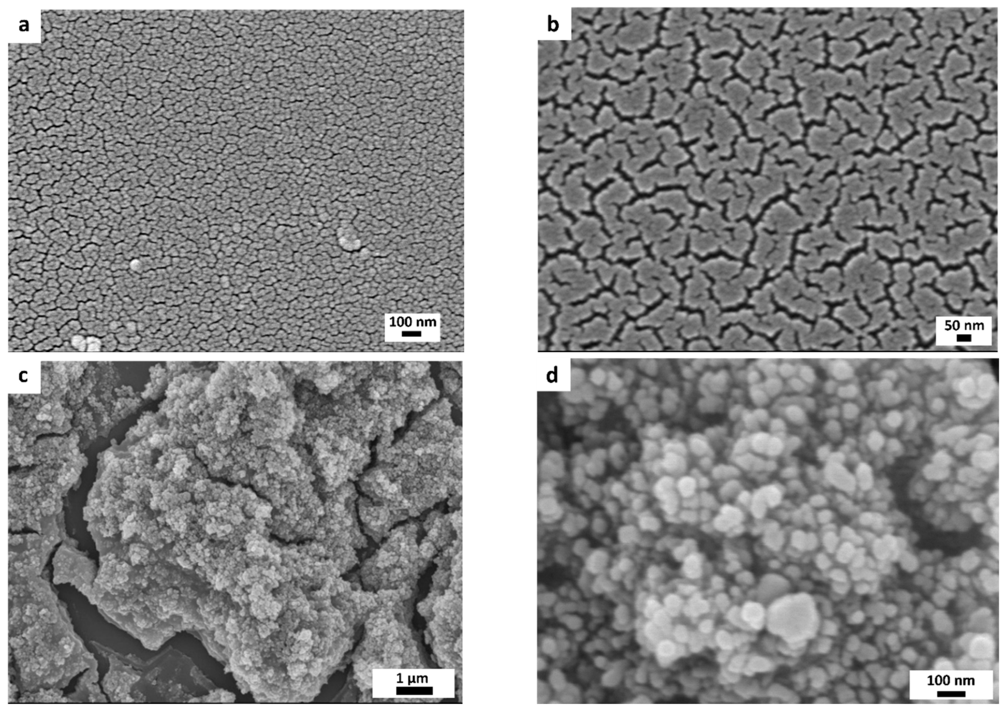
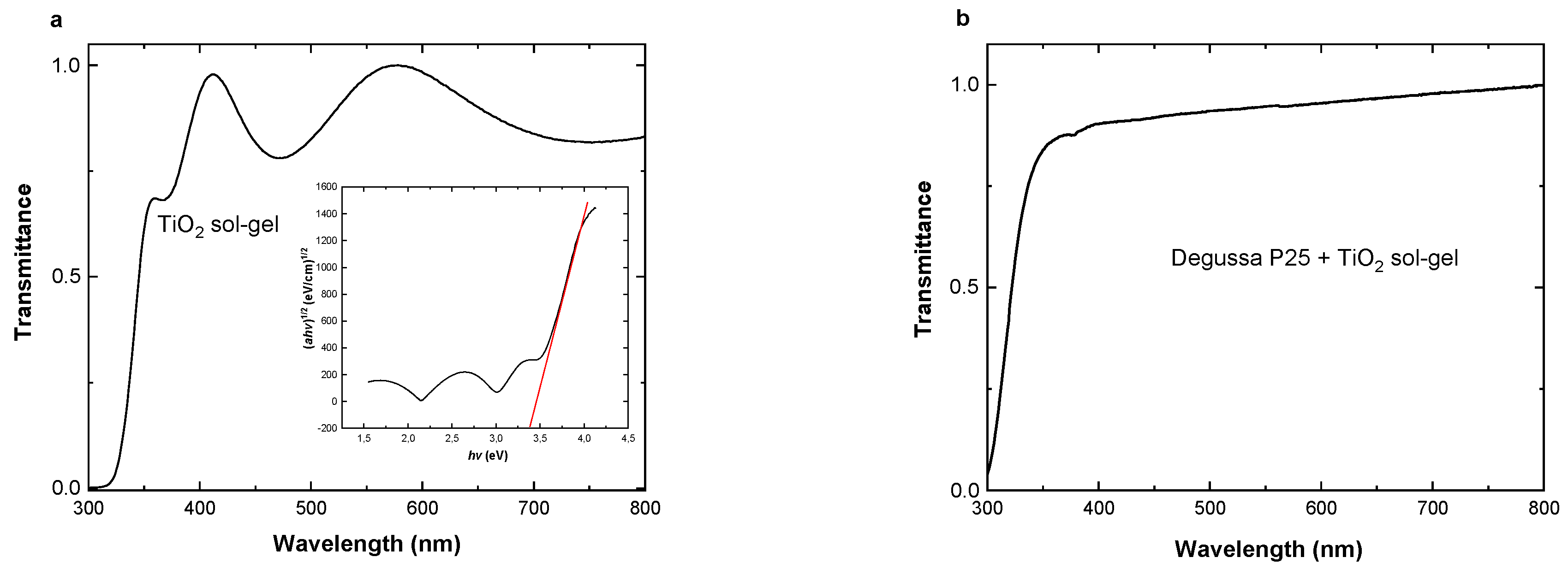
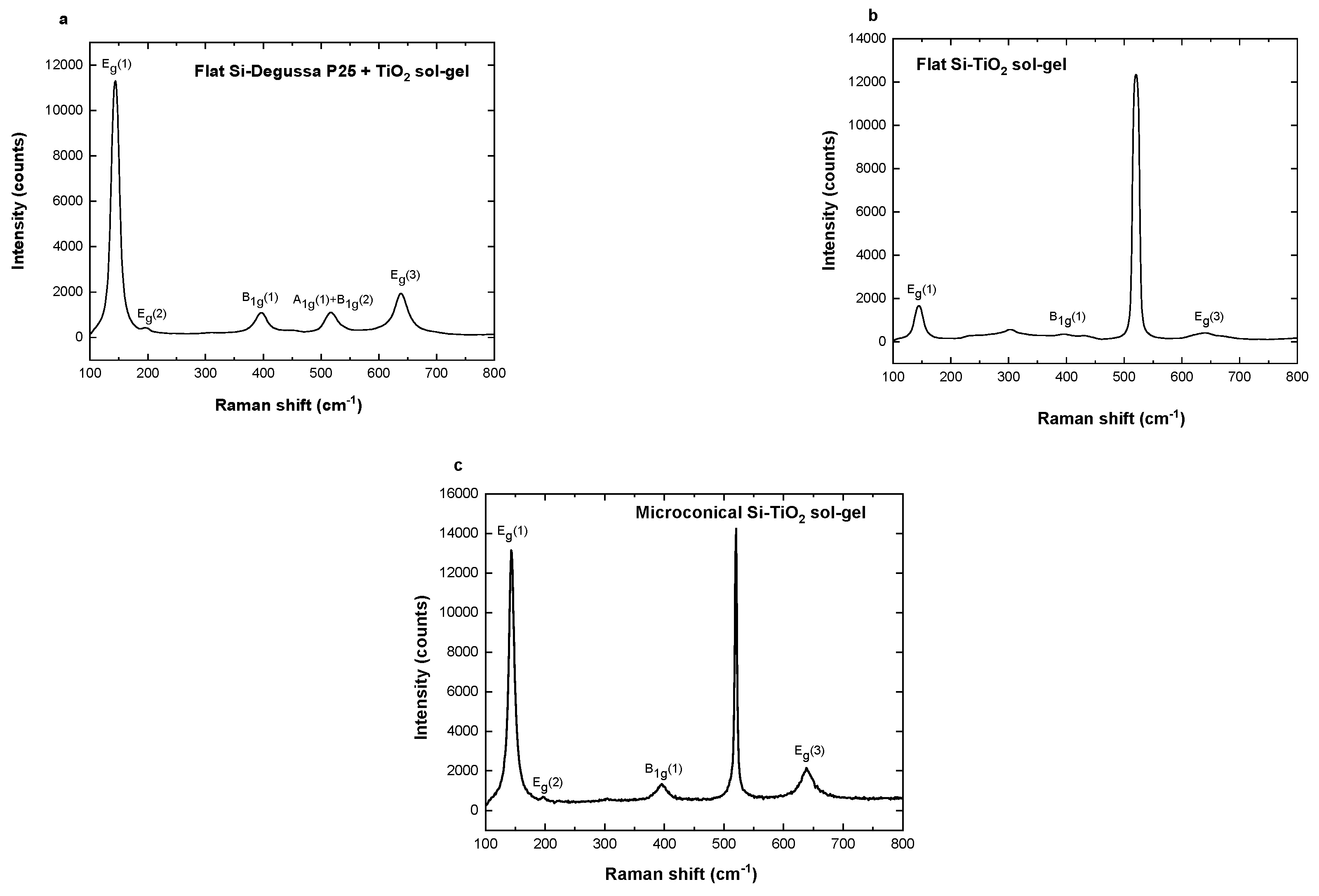
3.1. Morphological, Optical, and Structural Properties of Photocatalytic Surfaces

The XRD pattern of F-Si-solgel is depicted in Figure 1. This pattern confirms that only the (400) reflection of the flat silicon substrate is observed, consistent with its single crystal texture. None of the other red lines, representing the literature Bragg peaks of different silicon orientations, align with any experimental peak. Regarding TiO2, the experimental peaks align with the green lines, corresponding to the Bragg peaks of the anatase phase [53]. Notably, there are no indications of rutile or brookite, consistent with the findings from the Raman spectra. Both XRD and Raman analysis confirm that the TiO2 thin films are exclusively in the anatase phase.
Figure 2a,b show representative scanning electron microscope (SEM) images of laser-microstructured silicon substrates. The entire surface exhibits a semi-periodic array of conical microstructures. The geometric characteristics of these conical microstructures were quantified using image analysis software (ImageJ, 1.53v), with measurements conducted on at least 40 microcones on the SEM images (Table 1). Laser microstructuring is a cost-effective method, eliminating the need for cleanroom facilities and the use of masks [54]. The creation of this distinctive micromorphology relies on melting and interference phenomena, occurring on the nanosecond timescale, during laser irradiation of silicon wafers in an etching SF6 gas environment [32,55]. The tuning of experimental parameters, such as laser pulse duration, repetition rate, wavelength, gas pressure, and laser fluence, can significantly influence surface morphology [30,56]. For example, reducing the laser fluence results in the formation of rippled silicon surfaces, as depicted in Figure 2c,d. These ripples exhibit a semi-periodic structure, with an average peak height of 9.1 ± 0.2 μm. Notably, these structures represent the early stages of silicon microcone formation.
The morphology of F-Si-solgel is shown in the SEM images in Figure 3a,b. The TiO2 film exhibits notable uniformity, with nanometric cracks distributed across the surface. In the case of the reference F-Si-P25-solgel (Figure 3c,d), the surface displays both micro- and nanoscale roughness. The former stems from the porous structure and the latter from nanoparticle aggregations on the surface. The morphological characteristics shown in Figure 3 are in agreement with typical features observed in TiO2 thin films and commercial Degussa P25 films [13,57,58]. Figure 3c,d indicates that the composite TiO2 + Degussa P25 film predominantly adopts the morphology associated with Degussa P25. Thickness measurements for the TiO2 and TiO2 + Degussa films on flat silicon substrates indicate average values of 135 ± 15 nm and 2.0 ± 0.2 μm, respectively. The thickness of the films was measured by profilometry on partially coated substrates, where part of the substrate was covered by copper tape during spin coating.
The chemical composition of the samples was determined through EDX analysis. Figure 4a,b presents layered EDX images of F-Si-solgel. These images indicate the successful deposition of TiO2 coating on the flat silicon substrate, as evidenced by the uniformly distributed presence of oxygen and titanium throughout the film. Figure 4c,d maps the M-Si-solgel surface. From these figures, it is evident that the spin-coating method has successfully resulted in the coverage of the entire silicon structure by the TiO2 film. Therefore, the TiO2 film adopts the 3D microstructured silicon morphology and increased surface area. A higher concentration of titanium and oxygen is observed in the valleys between the microcones, as more material flows towards these areas during spin coating. The presence of silicon in both mapping distributions is attributed to the substrates on which the TiO2 films are deposited. Importantly, no contamination of carbon or other elements has been detected in either case, confirming the high purity of the samples.
Figure 5a,b depicts the UV–visible transmittance spectra of TiO2 and TiO2 + Degussa P25 films on glass substrates within the spectral range of 300–800 nm. Notably, both spectra exhibit a distinct absorption edge at 320 nm, and the films demonstrate high transparency within the visible range (400–700 nm). In the transmittance spectrum of TiO2, interference fringes are evident, attributed to the nanometric thickness of the film (135 nm) and reflections occurring from the back and front sides [13]. Conversely, this interference behavior is not observed in TiO2 + Degussa P25 films, owing to their one-order-of-magnitude-greater thickness (2 μm). From the Tauc plot presented in the inset of Figure 5a, the optical band gap (Eg) of TiO2 was calculated using the following equation: ( a h v ) n = K ( h v E g ) , where h is the Plank constant, ν is frequency of radiation, a is the absorption coefficient of the film, K is an experimental parameter depending on the photon energy, and n is a constant related to the nature of electronic transitions (TiO2 is an indirect semiconductor, n = 0.5 ) [50]. The Eg for TiO2, estimated by extrapolating the linear portion of ( a h v ) n versus h v , is determined to be 3.4 eV, consistent with the literature values [13,59]. The previously measured Eg for Degussa P25 is 3.15 eV [60].
Figure 6a presents the Raman spectrum of F-Si-P25-solgel, revealing five active modes of TiO2 + Degussa P25 on silicon. The distinct peaks at 144 cm−1, 196 cm−1, 397 cm−1, 517 cm−1, and 639 cm−1 correspond to the active modes Eg(1), Eg(2), B1g(1), A1g(1) + B1g(2), and Eg(3), respectively. According to research studies, these values are associated with the anatase phase of TiO2 [61]. No active mode of silicon is detected in this sample, attributed to the micrometric thickness of the film. Conversely, for F-Si-solgel and M-Si-solgel (Figure 6b,c), the A1g(1) + B1g(2) active mode is not detected due to the nanometric thickness of the sample and the coexistence of a strong Raman peak of silicon at the same Raman shift. Two Raman modes observed at 303 cm−1 and 520 cm−1 in these spectra correspond to the single crystal silicon substrate [62,63]. All other detected peaks are associated with the anatase phase of TiO2. Slight shifts in anatase Raman peaks (~2–3 cm−1) between the different samples may arise from differences in laboratory temperatures during measurements [13]. These observations collectively confirm that the developed TiO2 is in the anatase phase, with no signs of brookite or rutile phases.

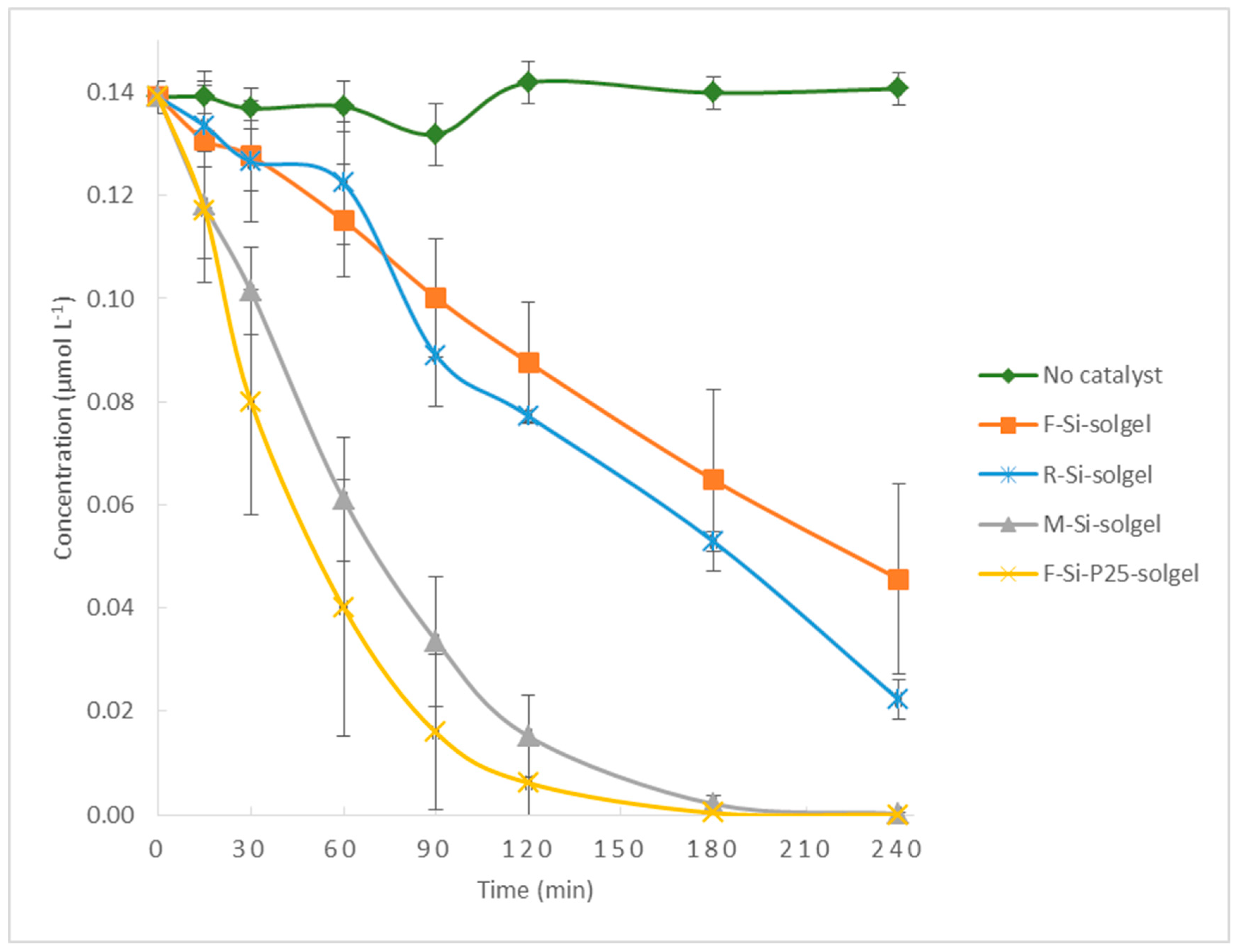
3.2. Photocatalytic Activity of Different Surfaces

Illumination of an aqueous solution of atrazine in the presence of all tested surfaces resulted in the decomposition of atrazine, whereas in their absence, the degradation was remarkably slow (Figure 7). Experiments in the absence of light showed adsorption of atrazine on the photocatalytic surfaces below 3%. Each data point in Figure 7 represents the average value of five independent experiments, carried out using five identical surfaces coated with the same photocatalytic material. Error bars correspond to the standard deviation of the five independent experiments and range from 0.007 to 0.018 μmol/L, 0.007 to 0.025 μmol/L, and 0.002 to 0.015 μmol/L for F-Si-solgel, F-Si-P25-solgel, and M-Si-solgel, respectively.
The observed rate constants, kobs, were determined for each photocatalytic surface assuming first-order kinetics and the results are summarized in Table 2. Only two experiments were carried out for the rippled R-Si-solgel surface, because the morphology of this sample was outside the main scope of this work and it was used only for comparison purposes. The best photocatalytic activity was observed for the reference TiO2 + Degussa F-Si-P25-solgel surface with a kobs mean value of 32.7 × 10⁻³ min−1. This value is one order of magnitude higher than the kobs of the F-Si-solgel surface (4.9 × 10⁻³ min−1), which consists of the same substrate (flat silicon) with the pure TiO2 coating. This difference demonstrates the photocatalytic efficiency of the coating alone. However, when the pure TiO2 film is deposited on the microconical silicon substrate (M-Si-solgel), kobs increases by one order of magnitude (24.1 × 10⁻³ min−1) and approaches the value of the reference F-Si-P25-solgel surface. This indicates the improvement in the photocatalytic efficiency of the surface due to the 3D micro-patterned morphology of the substrate.
The dependence of the photocatalytic improvement on the 3D geometry of the substrate is indicated by the results obtained with the rippled R-Si-solgel surface. Here, the same pure TiO2 coating is used, albeit with a smoother substrate morphology, consisting of microripples instead of microcones. The mean value of kobs for this surface (7.3 × 10⁻³ min−1) is between those of F-Si-solgel and M-Si-solgel, all with the same coating. This remarkable result indicates that the substrate morphology is a leading parameter of the photocatalytic process. Furthermore, the sensitivity of the measurements employed in this work is high enough to distinguish between different morphologies of the same length scale. The approximately threefold improvement of kobs for the M-Si-solgel compared with the R-Si-solgel is in agreement with the approximately threefold increase in the height of the microcones (29 μm) compared with the height of the microripples (9.1 μm). Figure S2 shows the dependence of kobs on the size of the microstructure. Therefore, the change in the specific surface area of the substrates is reflected in the change in the photocatalytic efficiency of the samples.
In order to investigate the effect of the substrate morphology on the TiO2 + Degussa P25 film photocatalytic activity, we carried out photocatalytic measurements on microconical silicon substrates coated with the composite TiO2 + Degussa P25 film. These surfaces exhibit a mean kobs equal to (38.5 ± 5.7) × 10−3 min−1, which is similar to the kobs value for TiO2 + Degussa P25 deposited on flat silicon (F-Si-P25-solgel), indicating that surface modification has no significant effect on their performance, unlike the results for the pure TiO2 films. SEM-EDX images of these samples, shown in Figure S3, indicate the TiO2 + Degussa P25 film does not coat the silicon microstructure conformally; rather, it is concentrated only in the valleys, leaving the silicon microcones uncoated. Therefore, in this case, the increased surface area of the substrate is not adopted by the TiO2 + Degussa P25 film and the photocatalytic efficiency is similar to the one of flat silicon substrates with this coating. This is in contrast to the pure TiO2 films, which coat both the valleys and microcones on the patterned silicon substrates as indicated in Figure 4, which results in an increase in their photocatalytic efficiency on these substrates.
The durability of the photocatalytic activity of the surfaces was also investigated. The reuse of the same surface for five sequential cycles resulted in no significant changes in their photocatalytic performance. The mean kobs values ± SD for F-Si-solgel, F-Si-P25-solgel, and R-Si-solgel were (4.3 ± 1.0) × 10−3, (40.7 ± 2.9) × 10−3, and (7.7 ± 1.8) × 10−3 min−1, respectively.
Moreover, the structural integrity of the surfaces is illustrated in Figure S4. The SEM images after photocatalysis experiments are very similar to the SEM images before photocatalysis (Figure 2), indicating the stability of the immobilized TiO2 surfaces.
During the photocatalytic process, several TPs of atrazine, namely CIAT, CAET, and CAAT, were identified with LC–MS/MS by comparing their characteristic transitions with those reported in the literature [64]. The MRM chromatograms of atrazine and the TPs that formed after illumination of atrazine for 60, 90, 120, and 180 min are depicted in Figures S5 and S6.
The photocatalytic activity of the most promising surface (M-Si-solgel) was also evaluated for the degradation of two other pollutants: (a) the persistent environmental pollutant 2,4,6-trichlorophenol, frequently found in water; and (b) the endocrine disruptor Bisphenol-a. The results show that this material can efficiently degrade both 2,4,6-trichlorophenol and Bisphenol-a, exhibiting kobs values 51.8 × 10⁻³ and 21.6 × 10⁻³ min−1, respectively. The photocatalytic degradation of the selected pollutants under UV-A irradiation is depicted in Figure S7.

4. Conclusions

The sol-gel process was employed to create thin TiO2 films in the anatase phase, which were spin-cast onto laser-microstructured silicon substrates, resulting in the formation of improved photocatalytic surfaces. To evaluate the photocatalytic efficacy of these surfaces, the degradation of atrazine in aqueous solution (environmentally relevant low concentration) under UV irradiation was measured.
The TiO2 films were thoroughly characterized using XRD, SEM-EDX, UV–Vis spectroscopy and Raman spectroscopy. They exhibited significantly enhanced photocatalytic activity when cast on laser-microstructured silicon. The photocatalytic activity of these materials was observed to undergo significant enhancement on laser-microstructured silicon (average kobs 24.1 × 10⁻³ min−1) in contrast to flat silicon (average kobs 4.9 × 10⁻³ min−1). This enhancement brought their performance close to that of sol-gel TiO2 fortified with Degussa P25, utilized as a reference material (kobs 32.7 × 10⁻³ min−1). Unlike pure TiO2 films, the composite TiO2 + Degussa films did not demonstrate enhanced photocatalytic activity when cast on microstrucured silicon substrates. SEM-EDX analysis showed this is due to the lack of conformal coating of the microstructured substrate by these films. The high sensitivity of the photocatalytic measuring device allowed us to discern between different substrate micromorphologies, revealing more efficient photocatalytic activity for TiO2 films on silicon microcones, compared with silicon microripples.
During the photocatalytic process, several TPs of atrazine, namely 2-chloro-4-(isopropylamino)-6-amino-s-triazine (CIAT), 2-chloro-4-amino-6-(ethylamino)-s-triazine (CAET), and 2-chloro-4.6-diamino-s-triazine (CAAT), were identified with LC–MS/MS. The stability of the photocatalytic surfaces was studied through multiple usage cycles, revealing that their activity remained consistent. SEM microscopy on these surfaces after photocatalysis experiments demonstrated that their morphology remains unchanged.
The photocatalytic activity of TiO2 films on laser-microstructured silicon was also evaluated for two other pollutants, i.e., 2,4,6-trichlorophenol and bisphenol-a (a frequent water pollutant and an endocrine disruptor, respectively), showing equally promising results with atrazine, demonstrating the wide application potential of these surfaces. These results, in combination with the immobilized state of the photocatalyst, leading to the elimination of expensive and time-consuming filtration post-processes, constitute an attractive photocatalytic system for efficient and affordable water treatment.

Supplementary Materials

The following supporting information can be downloaded at: https://www.mdpi.com/article/10.3390/app14073033/s1.

Author Contributions

Conceptualization, T.M.T., C.C., G.M., A.H. and M.K.; Data Curation, T.G., S.-K.Z., T.M.T., P.K., G.M., A.H. and M.K.; Formal Analysis, T.G., S.-K.Z. and T.M.T.; Methodology, T.G., S.-K.Z., T.M.T., S.V.S., G.M., A.H. and M.K.; Project Administration, T.M.T., C.C., A.H. and M.K.; Resources, T.M.T., C.C. and G.M.; Supervision, T.M.T., G.M., A.H. and M.K.; Visualization, T.G. and S.-K.Z.; Writing—Original Draft, T.G., S.-K.Z., T.M.T., C.C., E.B., G.M., A.H. and M.K.; Writing—Review and Editing, C.C., E.B., A.H. and M.K. All authors have read and agreed to the published version of the manuscript.

Funding

This research was co-financed by Greece and the European Union (European Regional Development Fund) through the Regional Operational Programme “Attica 2014–2020” in the context of the project “Photocatalytic reactors for water and liquid waste purification with immobilized photocatalysts on micro/nanopatterned surfaces” (MIS 5185074) under the Action “Research and Innovation Synergies in the Region of Attica”.

Institutional Review Board Statement

Not applicable.

Informed Consent Statement

Not applicable.

Data Availability Statement

The raw data supporting the conclusions of this article will be made available by the authors on request.

Acknowledgments

The authors would like to acknowledge V. Psycharis for XRD measurements and N.S. Tagiara for her help with Raman spectroscopy.

Conflicts of Interest

The authors declare no conflicts of interest. The funders had no role in the design of the study; in the collection, analyses, or interpretation of data; in the writing of the manuscript, or in the decision to publish the results.

References

  1. Hoffmann, M.R.; Martin, S.T.; Choi, W.; Bahnemann, D.W. Environmental Applications of Semiconductor Photocatalysis. Chem. Rev. 1995, 95, 69–96. [Google Scholar] [CrossRef]
  2. Legrini, O.; Oliveros, E.; Braun, A.M. Photochemical processes for water treatment. Chem. Rev. 1993, 93, 671–698. [Google Scholar] [CrossRef]
  3. Herrmann, J.-M. Heterogeneous photocatalysis: Fundamentals and applications to the removal of various types of aqueous pollutants. Catal. Today 1999, 53, 115–129. [Google Scholar] [CrossRef]
  4. Manassero, A.; Satuf, M.L.; Alfano, O.M. Photocatalytic reactors with suspended and immobilized TiO2: Comparative efficiency evaluation. Chem. Eng. J. 2017, 326, 29–36. [Google Scholar] [CrossRef]
  5. Liu, N.; Ming, J.; Sharma, A.; Sun, X.; Kawazoe, N.; Chen, G.; Yang, Y. Sustainable photocatalytic disinfection of four representative pathogenic bacteria isolated from real water environment by immobilized TiO2-based composite and its mechanism. Chem. Eng. J. 2021, 426, 131217. [Google Scholar] [CrossRef]
  6. Kennedy, A.J.; McQueen, A.D.; Ballentine, M.L.; May, L.R.; Fernando, B.M.; Das, A.; Klaus, K.L.; Williams, C.B.; Bortner, M.J. Degradation of microcystin algal toxin by 3D printable polymer immobilized photocatalytic TiO2. Chem. Eng. J. 2023, 455, 140866. [Google Scholar] [CrossRef]
  7. Balakrishnan, A.; Appunni, S.; Gopalram, K. Immobilized TiO2/chitosan beads for photocatalytic degradation of 2,4-dichlorophenoxyacetic acid. Int. J. Biol. Macromol. 2020, 161, 282–291. [Google Scholar] [CrossRef] [PubMed]
  8. Décsiné Gombos, E.; Krakkó, D.; Záray, G.; Illés, Á.; Dóbé, S.; Szegedi, Á. Laponite immobilized TiO2 catalysts for photocatalytic degradation of phenols. J. Photochem. Photobiol. A Chem. 2020, 387, 112045. [Google Scholar] [CrossRef]
  9. Rakshit, A.; Suresh, C.A. Immobilization. In Photocatalysis; CRC Press: Boca Raton, FL, USA, 2016. [Google Scholar]
  10. Byrne, C.; Subramanian, G.; Pillai, S.C. Recent advances in photocatalysis for environmental applications. J. Environ. Chem. Eng. 2018, 6, 3531–3555. [Google Scholar] [CrossRef]
  11. Ali, I.; Suhail, M.; Alothman, Z.A.; Alwarthan, A. Recent advances in syntheses, properties and applications of TiO2 nanostructures. RSC Adv. 2018, 8, 30125–30147. [Google Scholar] [CrossRef]
  12. Iwamura, S.; Motohashi, S.; Mukai, S.R. Development of an efficient CVD technique to prepare TiO2/porous-carbon nanocomposites for high rate lithium-ion capacitors. RSC Adv. 2020, 10, 38196–38204. [Google Scholar] [CrossRef] [PubMed]
  13. Moslah, C.; Kandyla, M.; Mousdis, G.A.; Petropoulou, G.; Ksibi, M. Photocatalytic Properties of Titanium Dioxide Thin Films Doped with Noble Metals (Ag, Au, Pd, and Pt). Phys. Status Solidi (A) Appl. Mater. Sci. 2018, 215, 1800023. [Google Scholar] [CrossRef]
  14. Miao, H.; Hu, X.; Fan, J.; Li, C.; Sun, Q.; Hao, Y.; Zhang, G.; Bai, J.; Hou, X. Hydrothermal synthesis of TiO2 nanostructure films and their photoelectrochemical properties. Appl. Surf. Sci. 2015, 358, 418–424. [Google Scholar] [CrossRef]
  15. El Habra, N.; Visentin, F.; Russo, F.; Galenda, A.; Famengo, A.; Rancan, M.; Losurdo, M.; Armelao, L. Supported MOCVD TiO2 Thin Films Grown on Modified Stainless Steel Mesh for Sensing Applications. Nanomaterials 2023, 13, 2678. [Google Scholar] [CrossRef] [PubMed]
  16. Inoue, N.; Yuasa, H.; Okoshi, M. TiO2 thin films prepared by PLD for photocatalytic applications. Appl. Surf. Sci. 2002, 197–198, 393–397. [Google Scholar] [CrossRef]
  17. Obregón, S.; Rodríguez-González, V. Photocatalytic TiO2 thin films and coatings prepared by sol–gel processing: A brief review. J. Sol Gel Sci. Technol. 2022, 102, 125–141. [Google Scholar] [CrossRef]
  18. Nanditha, P.P.; Suji, S.K. TiO2 as a Photocatalysts for Wastewater Treatment—A Review. In Proceedings of the SSRN International Conference on Emerging Trends in Engineering, Yukthi, Kozhikode, India, 10–12 April 2023. [Google Scholar]
  19. Mao, H.; Zhang, F.; Du, M.; Dai, L.; Qian, Y.; Pang, H. Review on synthesis of porous TiO2-based catalysts for energy conversion systems. Ceram. Int. 2021, 47, 25177–25200. [Google Scholar] [CrossRef]
  20. Zhang, H.; Du, G.; Lu, W.; Cheng, L.; Zhu, X.; Jiao, Z. Porous TiO2 hollow nanospheres: Synthesis, characterization and enhanced photocatalytic properties. CrystEngComm 2012, 14, 3793–3801. [Google Scholar] [CrossRef]
  21. Naik, A.P.; Mittal, H.; Wadi, V.K.S.; Sane, L.; Raj, A.S.S.; Alhassan, S.M.; Al Alili, A.R.; Bhosale, S.V.; Morajkar, P.P. Super porous TiO2 photocatalyst: Tailoring the agglomerate porosity into robust structural mesoporosity with enhanced surface area for efficient remediation of azo dye polluted waste water. J. Environ. Manag. 2020, 258, 110029. [Google Scholar] [CrossRef]
  22. Feng, X.; Pan, F.; Tran, B.Z.; Li, Y. Photocatalytic CO2 reduction on porous TiO2 synergistically promoted by atomic layer deposited MgO overcoating and photodeposited silver nanoparticles. Catal. Today 2020, 339, 328–336. [Google Scholar] [CrossRef]
  23. Ramasubbu, V.; Kumar, P.; Mothi, E.M.; Karuppasamy, K.; Kim, H.S.; Maiyalagan, T.; Shajan, X.S. Highly interconnected porous TiO2-Ni-MOF composite aerogel photoanodes for high power conversion efficiency in quasi-solid dye-sensitized solar cells. Appl. Surf. Sci. 2019, 496, 143646. [Google Scholar] [CrossRef]
  24. Tian, H.; Wang, S.; Zhang, C.; Veder, J.P.; Pan, J.; Jaroniec, M.; Wang, L.; Liu, J. Design and synthesis of porous ZnTiO3/TiO2 nanocages with heterojunctions for enhanced photocatalytic H2 production. J. Mater. Chem. A 2017, 5, 11615–11622. [Google Scholar] [CrossRef]
  25. Aleni, A.H.; Kretzschmar, N.; Jansson, A.; Ituarte, I.F.; St-Pierre, L. 3D printing of dense and porous TiO2 structures. Ceram. Int. 2020, 46, 16725–16732. [Google Scholar] [CrossRef]
  26. Wang, D.; Yu, R.; Chen, Y.; Kumada, N.; Kinomura, N.; Takano, M. Photocatalysis property of needle-like TiO2 prepared from a novel titanium glycolate precursor. Solid State Ion. 2004, 172, 101–104. [Google Scholar] [CrossRef]
  27. Latif, H.; Azher, Z.; Shabbir, S.A.; Rasheed, S.; Pervaiz, E.; Sattar, A.; Imtiaz, A. A novel leaves and needles like TiO2 (LNT) electron transfer layer (ETL) as an alternative to meso-porous TiO2 electron transfer layer (ETL) in perovskite solar cell. Opt. Mater. 2020, 109, 110281. [Google Scholar] [CrossRef]
  28. Wang, X.; Zhao, Y.; Molhave, K.; Sun, H. Engineering the surface/interface structures of titanium dioxide micro and nano architectures towards environmental and electrochemical applications. Nanomaterials 2017, 7, 382. [Google Scholar] [CrossRef] [PubMed]
  29. Raut, S.S.; Patil Girish, P.; Chavan Padmakar, G.; Sankapal Babasaheb, R. Vertically aligned TiO2 nanotubes: Highly stable electrochemical supercapacitor. J. Electroanal. Chem. 2016, 780, 197–200. [Google Scholar] [CrossRef]
  30. Amoako, G. Femtosecond Laser Structuring of Materials: A Review. Appl. Phys. Res. 2019, 11, 1. [Google Scholar] [CrossRef]
  31. Liu, X.; Coxon, P.R.; Peters, M.; Hoex, B.; Cole, J.M.; Fray, D.J. Black silicon: Fabrication methods, properties and solar energy applications. Energy Environ. Sci. 2014, 7, 3223–3263. [Google Scholar] [CrossRef]
  32. Lowndes, D.H.; Fowlkes, J.D.; Pedraza, A.J. Early stages of pulsed-laser growth of silicon microcolumns and microcones in air and SF6. Appl. Surf. Sci. 2000, 154–155, 647–658. [Google Scholar] [CrossRef]
  33. Pedraza, A.J.; Fowlkes, J.D.; Lowndes, D.H. Silicon microcolumn arrays grown by nanosecond pulsed-excimer laser irradiation. Appl. Phys. Lett. 1999, 74, 2322–2324. [Google Scholar] [CrossRef]
  34. Shen, M.Y.; Crouch, C.H.; Carey, J.E.; Mazur, E. Femtosecond laser-induced formation of submicrometer spikes on silicon in water. Appl. Phys. Lett. 2004, 85, 5694–5696. [Google Scholar] [CrossRef]
  35. Kanidi, M.; Dagkli, A.; Kelaidis, N.; Palles, D.; Aminalragia-Giamini, S.; Marquez-Velasco, J.; Colli, A.; Dimoulas, A.; Lidorikis, E.; Kandyla, M.; et al. Surface-Enhanced Raman Spectroscopy of Graphene Integrated in Plasmonic Silicon Platforms with Three-Dimensional Nanotopography. J. Phys. Chem. C 2019, 123, 3076–3087. [Google Scholar] [CrossRef]
  36. Tavera, T.; Perez, N.; Rodriguez, A.; Yurrita, P.; Olaizola, S.M.; Castano, E. Periodic patterning of silicon by direct nanosecond laser interference ablation. Appl. Surf. Sci. 2011, 258, 1175–1180. [Google Scholar] [CrossRef]
  37. Trtica, M.S.; Gakovic, B.M.; Radak, B.B.; Batani, D.; Desai, T.; Bussoli, M. Periodic surface structures on crystalline silicon created by 532 nm picosecond Nd:YAG laser pulses. Appl. Surf. Sci. 2007, 254, 1377–1381. [Google Scholar] [CrossRef]
  38. Lv, J.; Zhang, T.; Zhang, P.; Zhao, Y.; Li, S. Review application of nanostructured black silicon. Nanoscale Res. Lett. 2018, 13, 110. [Google Scholar] [CrossRef] [PubMed]
  39. Li, G.; Zhang, Z.; Wu, P.; Wu, S.; Hu, Y.; Zhu, W.; Li, J.; Wu, D.; Li, X.; Chu, J. One-step facile fabrication of controllable microcone and micromolar silicon arrays with tunable wettability by liquid-assisted femtosecond laser irradiation. RSC Adv. 2016, 6, 37463–37471. [Google Scholar] [CrossRef]
  40. Kanidi, M.; Papagiannopoulos, A.; Matei, A.; Dinescu, M.; Pispas, S.; Kandyla, M. Functional surfaces of laser-microstructured silicon coated with thermoresponsive PS/PNIPAM polymer blends: Switching reversibly between hydrophilicity and hydrophobicity. Appl. Surf. Sci. 2020, 527, 146841. [Google Scholar] [CrossRef]
  41. Park, J.K.; Yang, Z.; Kim, S. Black Silicon/Elastomer Composite Surface with Switchable Wettability and Adhesion between Lotus and Rose Petal Effects by Mechanical Strain. ACS Appl. Mater. Interfaces 2017, 9, 33333–33340. [Google Scholar] [CrossRef]
  42. Gao, X.; Guo, Z. Biomimetic Superhydrophobic Surfaces with Transition Metals and Their Oxides: A Review. J. Bionic Eng. 2017, 14, 401–439. [Google Scholar] [CrossRef]
  43. Hazell, G.; May, P.W.; Taylor, P.; Nobbs, A.H.; Welch, C.C.; Su, B. Studies of black silicon and black diamond as materials for antibacterial surfaces. Biomater. Sci. 2018, 6, 1424–1432. [Google Scholar] [CrossRef] [PubMed]
  44. EN 17120:2019; Photocatalysis—Water purification—Performance of Photocatalytic Materials by Measurement of Phenol Degradation. CEN: Brussels, Belgium, 2019.
  45. ISO 10676:2010; Test Method for Water Purification Performance of Semiconducting Photocatalytic Materials by Measurement of Forming Ability of Active Oxygen. ISO: London, UK, 2010.
  46. ISO 10678:2010; Determination of Photocatalytic Activity of Surfaces in an Aqueous Medium by Degradation of Methylene Blue. ISO: London, UK, 2010.
  47. Mills, A.; Hill, C.; Robertson, P.K.J. Overview of the current ISO tests for photocatalytic materials. J. Photochem. Photobiol. A Chem. 2012, 237, 7–23. [Google Scholar] [CrossRef]
  48. Hiskia, A.; Ecke, M.; Troupis, A.; Kokorakis, A.; Hennig, H.; Papaconstantinou, E. Sonolytic, photolytic, and photocatalytic decomposition of atrazine in the presence of polyoxometalates. Environ. Sci. Technol. 2001, 35, 2358–2364. [Google Scholar] [CrossRef] [PubMed]
  49. Frysali, M.A.; Papoutsakis, L.; Kenanakis, G.; Anastasiadis Spiros, H. Functional Surfaces with Photocatalytic Behavior and Reversible Wettability: ZnO Coating on Silicon Spikes. J. Phys. Chem. C 2015, 119, 25401–25407. [Google Scholar] [CrossRef]
  50. Priyalakshmi Devi, K.; Goswami, P.; Chaturvedi, H. Fabrication of nanocrystalline TiO2 thin films using Sol-Gel spin coating technology and investigation of its structural, morphology and optical characteristics. Appl. Surf. Sci. 2022, 591, 153226. [Google Scholar] [CrossRef]
  51. Starinskiy, S.V.; Rodionov, A.A.; Shukhov, Y.G.; Safonov, A.I.; Maximovskiy, E.A.; Sulyaeva, V.S.; Bulgakov, A.V. Formation of periodic superhydrophilic microstructures by infrared nanosecond laser processing of single-crystal silicon. Appl. Surf. Sci. 2020, 512, 145753. [Google Scholar] [CrossRef]
  52. Parra, S.; Elena Stanca, S.; Guasaquillo, I.; Ravindranathan Thampi, K. Photocatalytic degradation of atrazine using suspended and supported TiO2. Appl. Catal. B Environ. 2004, 51, 107–116. [Google Scholar] [CrossRef]
  53. Ijadpanah-Saravy, H.; Safari, M.; Khodadadi-Darban, A.; Rezaei, A. Synthesis of Titanium Dioxide Nanoparticles for Photocatalytic Degradation of Cyanide in Wastewater. Anal. Lett. 2014, 47, 1772–1782. [Google Scholar] [CrossRef]
  54. Fan, Z.; Cui, D.; Zhang, Z.; Zhao, Z.; Chen, H.; Fan, Y.; Li, P.; Zhang, Z.; Xue, C.; Yan, S. Recent progress of black silicon: From fabrications to applications. Nanomaterials 2021, 11, 41. [Google Scholar] [CrossRef]
  55. Crouch, C.H.; Carey, J.E.; Warrender, J.M.; Aziz, M.J.; Mazur, E.; Genin, F.Y. Comparison of structure and properties of femtosecond and nanosecond laser-structured silicon. Appl. Phys. Lett. 2004, 84, 1850–1852. [Google Scholar] [CrossRef]
  56. Kotsifaki, D.G.; Kandyla, M.; Lagoudakis, P.G. Near-field enhanced optical tweezers utilizing femtosecond-laser nanostructured substrates. Appl. Phys. Lett. 2015, 107, 211111. [Google Scholar] [CrossRef]
  57. Znad, H.; Ang, M.H.; Tade, M.O. Ta/TiO2- and Nb/TiO2-mixed oxides as efficient solar photocatalysts: Preparation, characterization, and photocatalytic activity. Int. J. Photoenergy 2012, 2012, 548158. [Google Scholar] [CrossRef]
  58. Subramanian, A.; Wang, H.W. Effect of hydroxyl group attachment on TiO2 films for dye-sensitized solar cells. Appl. Surf. Sci. 2012, 258, 7833–7838. [Google Scholar] [CrossRef]
  59. Li, D.; Zhang, J.; Shao, L.; Chen, C.; Liu, G.; Yang, Y. Preparation and photocatalytic properties of nanometer TiO2 thin films by improved ultrasonic spray pyrolysis. Rare Met. 2011, 30, 233–237. [Google Scholar] [CrossRef]
  60. Meier, A.J.; Hintze, P.E.; Devor, R.; Maloney, P.; Mazyck, D.W.; Coutts, J.L.; Bauer, B.M.; Surma, J.; Shah, M.G. Visible-Light-Responsive Photocatalysis: Ag-Doped TiO2 Catalyst Development and Reactor Design Testing. In Proceedings of the 46th International Conference on Environmental Systems, Vienna, Austria, 10–14 July 2016. [Google Scholar]
  61. Parker, J.H.; Feldman, D.W.; Ashkin, M. Raman Scattering by Silicon and Germanium. Phys. Rev. 1967, 155, 712–714. [Google Scholar] [CrossRef]
  62. Parker, J.C.; Siegel, R.W. Raman Microprobe Study of Nanophase TiO2 and Oxidation-Induced Spectral Changes. J. Mater. Res. 1990, 5, 1246–1252. [Google Scholar] [CrossRef]
  63. Zhang, W.F.; He, Y.L.; Zhang, S.; Yin, Z.; Chen, Q. Raman scattering study on anatase TiO2 nanocrystals. J. Phys. D Appl. Phys. 2000, 33, 912–916. [Google Scholar] [CrossRef]
  64. Liang, S.; Dong, X.; Su, M.; Sun, H. Analysis of herbicide atrazine and its degradation products in cereals by ultra-performance liquid chromatography-mass spectrometry. Anal. Methods 2016, 8, 3599–3604. [Google Scholar] [CrossRef]
Figure 1. XRD pattern of TiO2 film on flat silicon (red and green lines correspond to the literature Bragg peaks of silicon and anatase phase of TiO2, respectively).
Applsci 14 03033 g001
Figure 2. SEM images of (a,b) silicon microcones and (c,d) rippled silicon surfaces. All images are taken at a side (45°) view.
Applsci 14 03033 g002
Figure 3. SEM images of (a,b) TiO2 and (c,d) TiO2 + Degussa P25 thin films on flat silicon substrates.
Applsci 14 03033 g003
Figure 4. Layered EDX images of TiO2 thin film on (a) flat silicon and (c) microconical silicon substrates. Image (c) is taken at side (20°) view. (b,d) Mapping distribution of elements.
Applsci 14 03033 g004
Figure 5. (a) UV–visible transmittance spectrum for TiO2 film on glass. The inset shows the corresponding Tauc plot. (b) UV–visible transmittance spectrum for TiO2 + Degussa P25 film on glass.
Applsci 14 03033 g005
Figure 6. Raman spectra of (a) F-Si-P25-solgel, (b) F-Si-solgel, and (c) M-Si-solgel.
Applsci 14 03033 g006
Figure 7. Direct photolysis and photocatalytic degradation of atrazine (0.139 μmol L−1) under UV-A irradiation (λmax = 365 nm) in the presence of the different photocatalytic surfaces. Average value and error bars of five independent experiments for each surface.
Applsci 14 03033 g007
Table 1. Geometrical characteristics of silicon microcones.
Half-Height DiameterHeightDistance between Neighboring Microcones
[μm][μm][μm]
6.8 ± 0.229.0 ± 0.79.0 ± 0.4
Table 2. Observed rate constants (kobs) for the four photocatalytic surfaces (n = 5).
kobs (min−1)
F-Si-solgelF-Si-P25-solgelR-Si-solgelM-Si-solgel
Experiment 15.1 × 10−339.1 × 10−37.8 × 10−322.5 × 10⁻³
Experiment 23.9 × 10−343.6 × 10−36.8 × 10−318.9 × 10⁻³
Experiment 33.6 × 10−340.7 × 10⁻³n.a. 221.3 × 10⁻³
Experiment 48.8 × 10−317.5 × 10⁻³n.a.26.0 × 10−3
Experiment 53.1 × 10−322.5 × 10⁻³n.a.31.7 × 10−3
Mean value ± SD 1(4.9 ± 2.3) × 10−3(32.7 ± 11.8) × 10−3(7.3 ± 0.7) × 10−3(24.1 ± 5.0) × 10−3
1 Standard deviation. 2 Data not available.
Disclaimer/Publisher’s Note: The statements, opinions and data contained in all publications are solely those of the individual author(s) and contributor(s) and not of MDPI and/or the editor(s). MDPI and/or the editor(s) disclaim responsibility for any injury to people or property resulting from any ideas, methods, instructions or products referred to in the content.

