Article

A Broadband Millimeter-Wave 5G Low Noise Amplifier Design in 22 nm Fully Depleted Silicon-on-Insulator (FD-SOI) CMOS

1
Department of Electrical and Computer Engineering, Texas Tech University, Lubbock, TX 79409, USA
2
NoiseFigure Research Inc., Renton, WA 98057, USA
*
Author to whom correspondence should be addressed.
Appl. Sci. 2024, 14(7), 3080; https://doi.org/10.3390/app14073080
Submission received: 27 February 2024 / Revised: 27 March 2024 / Accepted: 4 April 2024 / Published: 6 April 2024
(This article belongs to the Special Issue Advanced Electronics and Digital Signal Processing)

Abstract

:
This paper presents a broadband millimeter-wave (mm-Wave) low noise amplifier (LNA) designed in a 22 nm fully depleted silicon-on-insulator (FD-SOI) CMOS technology. Electromagnetic (EM) simulations suggest that the LNA has a 3-dB bandwidth (BW) from 17.8 to 42.4 GHz and a fractional bandwidth (FBW) of 81.7%, covering the key frequency bands within the mm-Wave 5G FR2 band, with its noise figure (NF) ranging from 2.9 to 4.9 dB, and its input-referred 1-dB compression point (IP1dB) of −17.9 dBm and input-referred third-order intercept point (IIP3) of −8.5 dBm at 28 GHz with 15.8 mW DC power consumption (PDC). Using the FOM (figure-of-merit) developed for broadband LNAs (FOM = 20 × log((Gain[V/V] × S21-3 dB-BW [GHz])/(PDC [mW] × (F-1)))), this LNA achieves a competitive FOM (FOM = 18.9) among reported state-of-the-art mm-Wave LNAs in the literature.

1. Introduction

As the demand for higher data-rate wireless communication keeps increasing, there is a strong interest in utilizing mm-Wave frequencies due to its wider available BW. As a result, mm-Wave bands such as the 5G FR2 band have been adopted, which makes the design of RF (radio-frequency) integrated circuits operating at these frequency ranges widely studied [1,2,3,4,5,6,7]. Being at the RF front end of a receiver, an LNA is one of the most important components of the receiver since its NF and linearity directly impact the sensitivity and selectivity of the receiver system [8]. The challenge in broadband millimeter-wave LNA design is to simultaneously achieve low NF, power gain and linearity across a wide BW while maintaining low power consumption. Recent broadband mm-Wave LNAs have achieved wide BW using several techniques, such as through the implementation of gate-source feedback with transformers, pole-tuning, dual-resonance techniques, etc. [2,3,4,5]. Gate-source feedback using transformers provides good input matching bandwidth due to transformers being high-order matching networks, in addition to the bandwidth extension by feedback [3,5]. The pole-tuning technique manipulates poles and zeros around the resonant frequencies to adjust the bandwidth of the matching network [4]. Dual resonance [2,3] utilizes the non-negligible gate-drain capacitance at mm-Wave frequencies to have the interstage matching provide the second S11 resonance for improved input matching. Since several regulation organizations around the world have proposed upcoming standards for mm-Wave 5G, it is worth looking into frequency bands such as 28, 37 and 39 GHz by the Federal Communications Commission (FCC) in the US and various bands from 24.25 to 42.5 GHz, etc. by the International Telecommunication Union [9]. Having one broadband LNA instead of multiple narrowband LNAs could potentially save cost, area, and power for 5G/B5G systems and open up more applications that can benefit from mm-Wave’s available BW. Therefore, the motivation of this study is to design an LNA with broad bandwidth and low NF that can cover the key FR2 bands. The targeted S21 3-dB BW for this LNA design is 24 GHz to 42 GHz to cover the key 5G FR2 bands, and the lowest NF should be less than 3 dB in the targeted BW as in the literature [1,2,3,4,5,6,7]. As we aim to design mm-Wave phased-array receiver systems in the future, a relaxed linearity specification of IIP3 better than −15 dBm was targeted [5]. With these specifications in mind, we designed an mm-Wave two-stage broadband LNA where we devised a gain compensation technique in frequency, in addition to incorporating resistive feedback in the first stage of the LNA to improve input matching and gain flatness.
The paper is organized as follows. Section 2 introduces the LNA design strategies, describing the device selection process as well as the core design methodology. Section 3 presents the PEX (post-layout parasitic extraction) simulated results using an EM solver vs. the traditional lump-element PEX simulations with several parasitic extraction options: R (i.e., R, resistance only), R + C (i.e., RC, resistance, capacitance to ground), and R + C + CC (i.e., RCC, resistance, capacitance to ground, and coupled capacitance between any two metal traces) using Mentor/Siemens Calibre xACT. Finally, we summarize our design performance against the state-of-the-art broadband mm-Wave and Ka-band LNAs in the literature, and Section 4 concludes the paper.

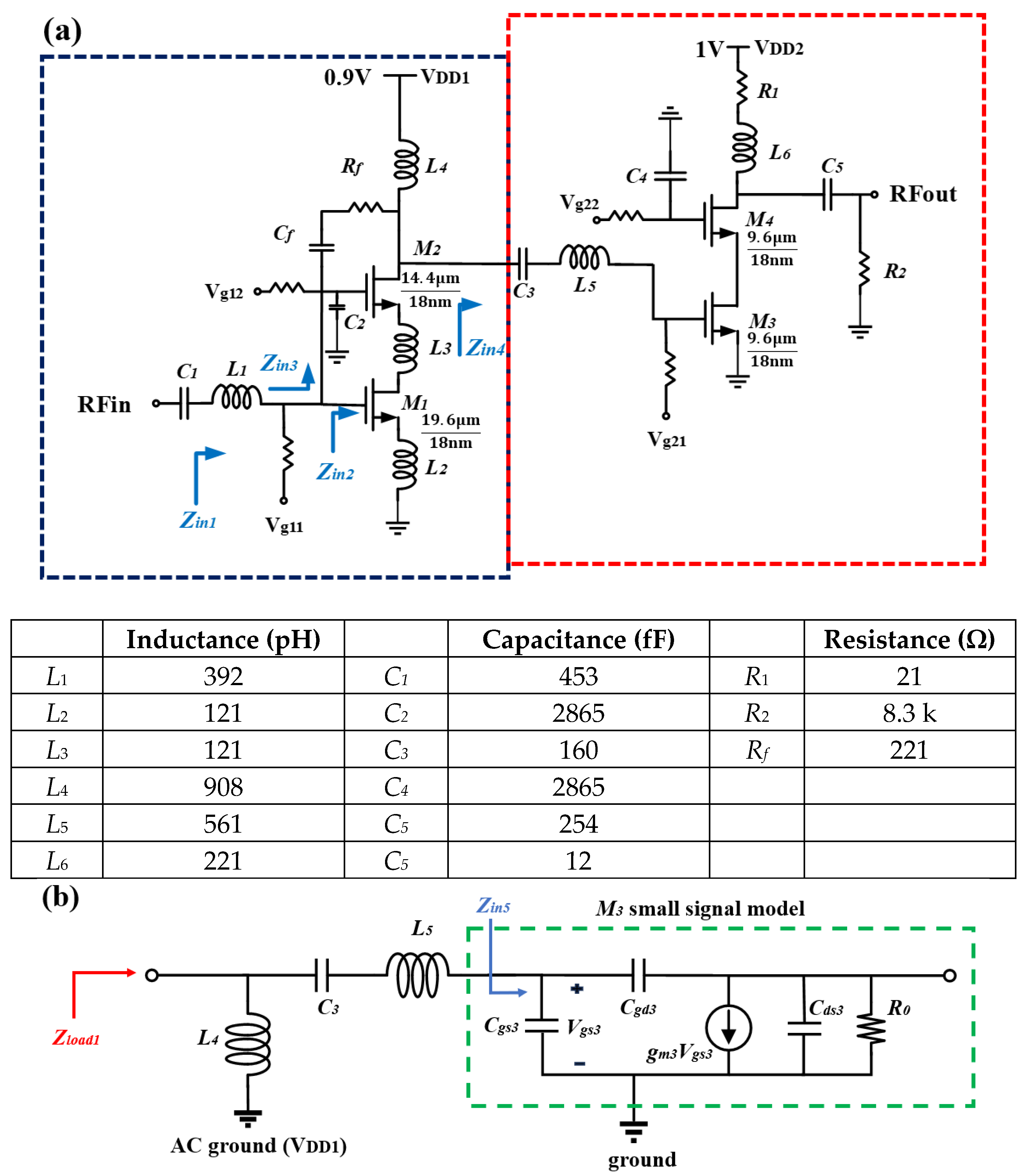
2. LNA Design Methodology

This section covers the entire LNA design process in pre-PEX simulations. Minimum noise figure, noise circle, maximum available gain (for fMAX), H parameter (for fT), S parameter (for S11, S21), power gain and power gain circle simulations are presented in this section.

2.1. 22 nm FD-SOI CMOS Technology

This work has been designed using GlobalFoundries’ 22FDX technology, which is an advanced 22 nm FD-SOI CMOS process [10,11]. We created a single-ended, two-stage cascode-cascode mm-Wave broadband LNA. Devices within this technology exhibit reduced off-state leakage current thanks to the presence of a thin buried oxide layer (BOX) and a fully depleted channel [9,10]. Our design specifically utilizes SLVTNFET (i.e., super low threshold voltage N-MOSFET), which is capable of achieving an impressive peak fT of approximately 350 GHz and a peak fMAX of around 370 GHz for the smallest device [11,12,13]. Additionally, this technology enables back-gate biasing of the MOSFETs, offering the ability to adjust the threshold voltage (VT) through back-gate controls, although we did not employ this feature in our work [13].

2.2. Device Selection

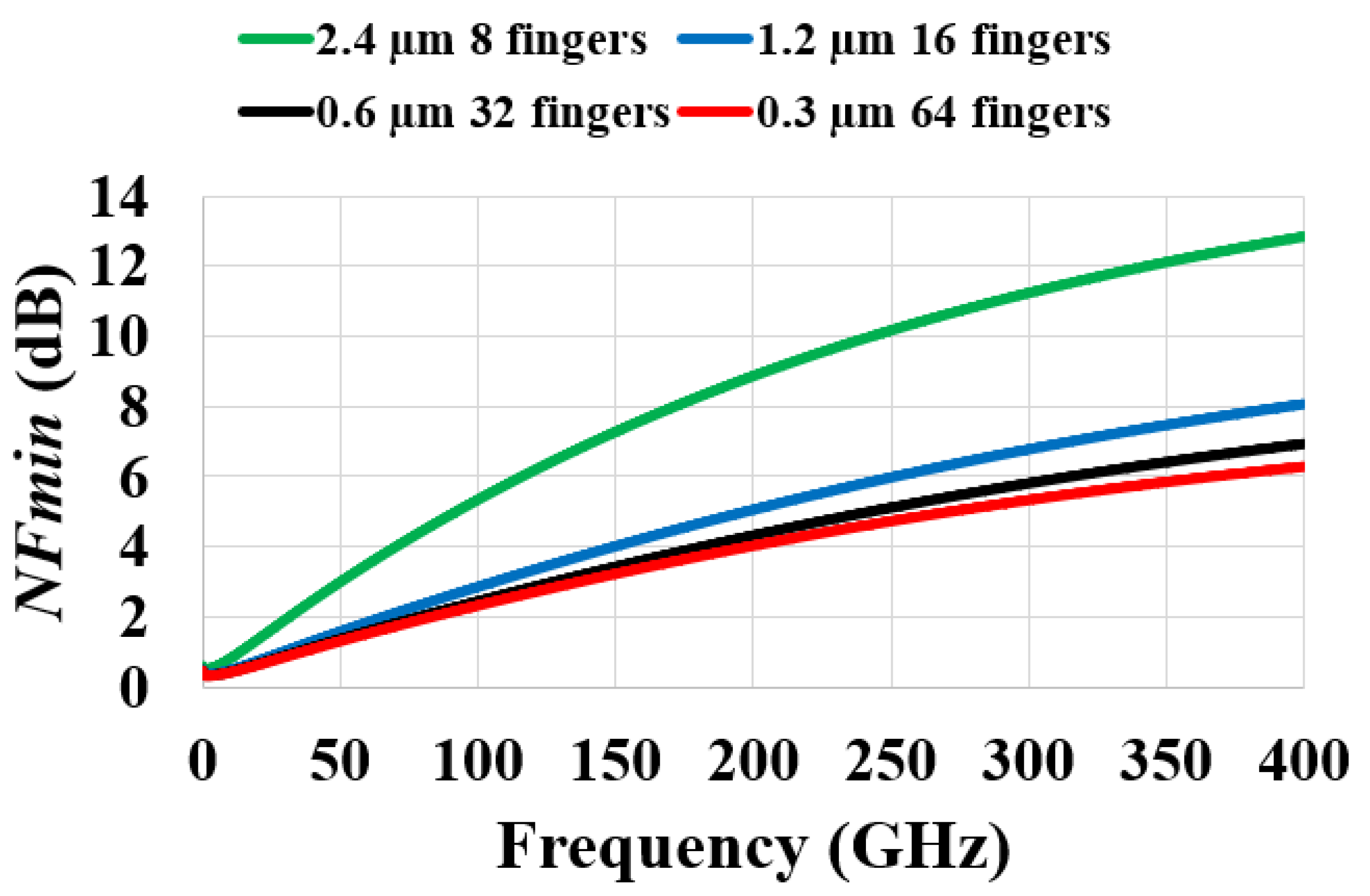
2.2.1. Finger Width and Number of Fingers

In addition to its small signal gain, NF is one of the most essential design specifications of an LNA. As the finger size and layout of the transistors contribute to much of the gate resistance and other parasitics of the NMOS device, choosing the optimized finger width can substantially help reduce the minimum noise figure (NFmin). Figure 1 shows the pre-layout (or pre-PEX) simulations of the NFmin of a single NFET as a function of the frequency of various finger widths from 0.3 μm to 2.4 μm under a constant total width of 19.2 μm (total width = finger width × number of fingers). The NMOS transistor was biased with a gate voltage of 0.45 V and a drain voltage of 0.9 V. NFmin increases with frequency and is lowest in the case where a finger width of 0.3 µm was simulated. Therefore, we chose 0.3 µm finger width for all the NMOS devices in this design.

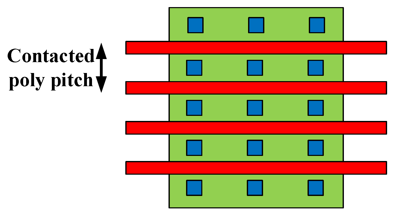
2.2.2. Contact Poly Pitch (CPP)

As the intrinsic gain of an amplifier drops with frequency, using transistors with high fT/fMAX in LNA design is essential at mm-Wave frequencies. As high fT is usually associated with lower device NF, we have biased several N-MOSFET to reach fT above ~340 GHz to study their noise performance, as shown in Table 1. However, unlike the device’s NFmin, fT is known to be less sensitive to the transistor’s layout parasitics resistance and capacitance. Similar to NFmin, fMAX is highly dependent on the layout of the transistor, and since GF’s 22FDX offers options to vary the contact poly pitch (CPP, see Figure 2), the effects of CPP on NFmin and fMAX were explored in pre-PEX simulation [14]. As shown in Table 1, transistors with pitches that are 208 nm (CPP2x) have higher fMAX than the narrower pitched 104 nm (CPP1x) devices, and their differences become more significant as the total width is increased. Similarly, NFmin at 28 GHz is consistently better for the CPP2x devices as they are lower than the CPP1x devices. This is because a wide pitch in CPP2x devices can fit more drain and source contacts, and due to the increased contact areas, the drain and source resistance is effectively reduced and, therefore, both NFmin and fMAX are improved [14]. Consequently, a CPP of 208 nm is selected for all NMOS devices used in this design.

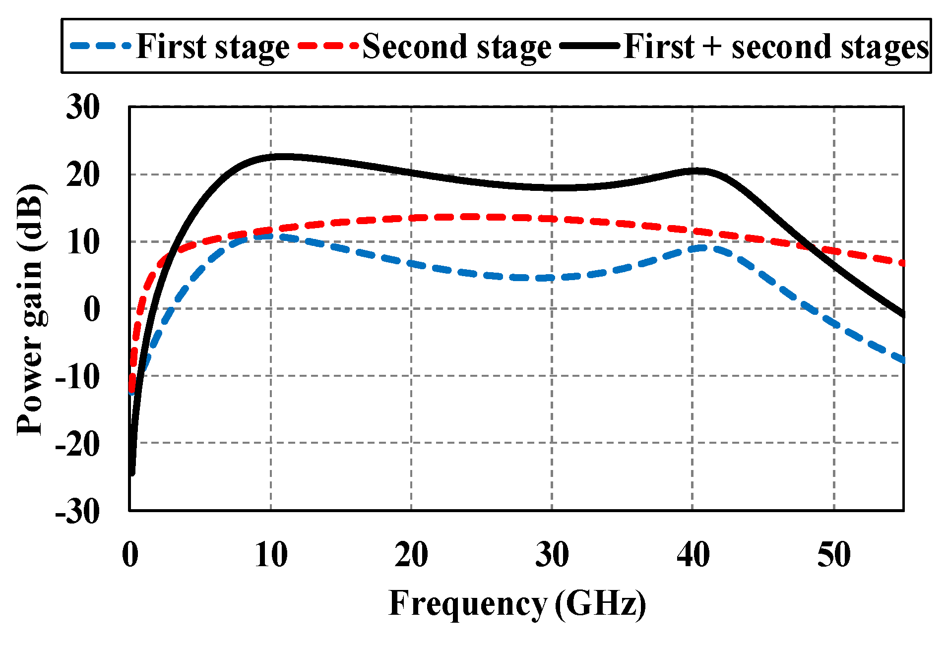
2.3. Two-Stage Gain Compensation

An important design criterion for broadband LNAs is flat gain, and one way is to synthesize a load with a high-order matching network such that the load impedance does not vary much with frequency. However, the tradeoff is that it may take up more die space, which incurs higher costs. Thus, in this work, we create a two-stage broadband LNA, where each stage has complementary gain responses across frequencies to each other. Figure 3 shows a simplified schematic of the two-stage LNA, where all passives and active components are integrated on-chip. The first stage’s load Zload1, shown in Figure 3b, is calculated as
Z l o a d 1 = j ω L 4 Z i n 5 + 1 j ω C 3 + j ω L 5 = ω 2 Z i n 5 L 4 L 5 ω 2 1 + L 4 ω 2 + j { ω 3 Z i n 5 2 + ω L 4 C 3 [ 1 C 3 + C 3 L 4 L 5 ω 2 L 4 + L 5 L 5 ω 2 + 1 + L 4 ] } [ 1 C 3 ω 2 L 4 + L 5 ] 2 + ω 2 Z i n 5 2
Zload1 is a resonant circuit that was designed to provide two resonant frequencies, resulting in high voltage gains with large impedances at these frequencies, approximately around 10 and 41 GHz. Components C3, L4 and L5 are tuned such that Zload1 provides larger power transfer at these frequencies. The values of L4 and C3 are responsible for controlling the first (lower) resonant frequency, while C3, L5, and the gate-source capacitance of M3 are used to adjust the second (higher) resonant frequency. The separation of the gain peaks should be carefully chosen. If the peak separation is small, we cannot achieve wide S21 bandwidth; however, if the separation is too wide, a simple L section output matching network in the second stage would be unable to compensate for the gain droop sufficiently because a one-stage L matching network provides narrowband frequency response. Since a one-stage cascode alone cannot provide wide S21 bandwidth, the second stage of the LNA’s gain frequency response is purposely designed to align its gain peak with the gain trough of the first stage, as shown in Figure 4. This design arrangement ensures that the overall gain remains relatively consistent across a wider range of frequencies, achieving a broadband LNA.
To synthesize the second stage’s load to achieve complementary gain responses in frequency between the first and second stages, we may observe the power gain circles for the full LNA minus the second stage’s load at various frequencies such as 24, 30 and 40 GHz in Figure 5. Using these gain circles, we would know how the load impedance should vary on the Smith Chart such that the second stage’s load can mitigate the gain droops in the first stage. Instead of aiming to achieve relatively smaller changes in load impedance versus frequency, we chose to design the output matching network that achieves a similar distance from the gain circles at their given frequencies. In Figure 5, even though the load impedance locus changes from 24 GHz to 40 GHz, the impedances reside in the 24, 26 and 25 dB power gain circles for 24, 30 and 40 GHz, respectively, meaning a frequency-dependent load can provide the LNA a wide gain BW. We would like to point out that the gain from the gain circles assumes matching using lossless components, so it is naturally higher than matching the load using real on-chip components.
An alternative way of looking at this would be to simply observe the region where the gain droop occurs (between 20 and 30 GHz) and construct a second stage’s load that has its gain peak and provides peak power transfer at the first stage’s gain droop region. Since the gain droop region is more narrowband, one L matching network would provide a single gain peak such that it would compensate for the gain droop of the first stage, achieving an overall wide gain bandwidth.

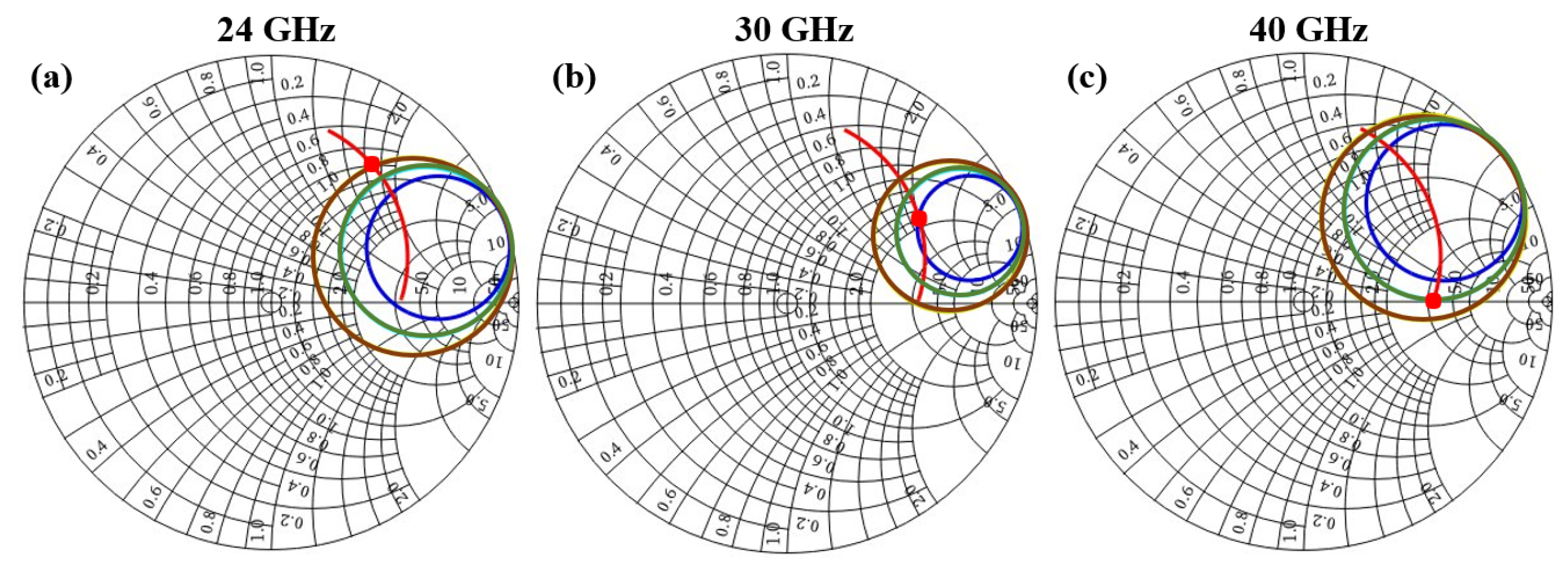
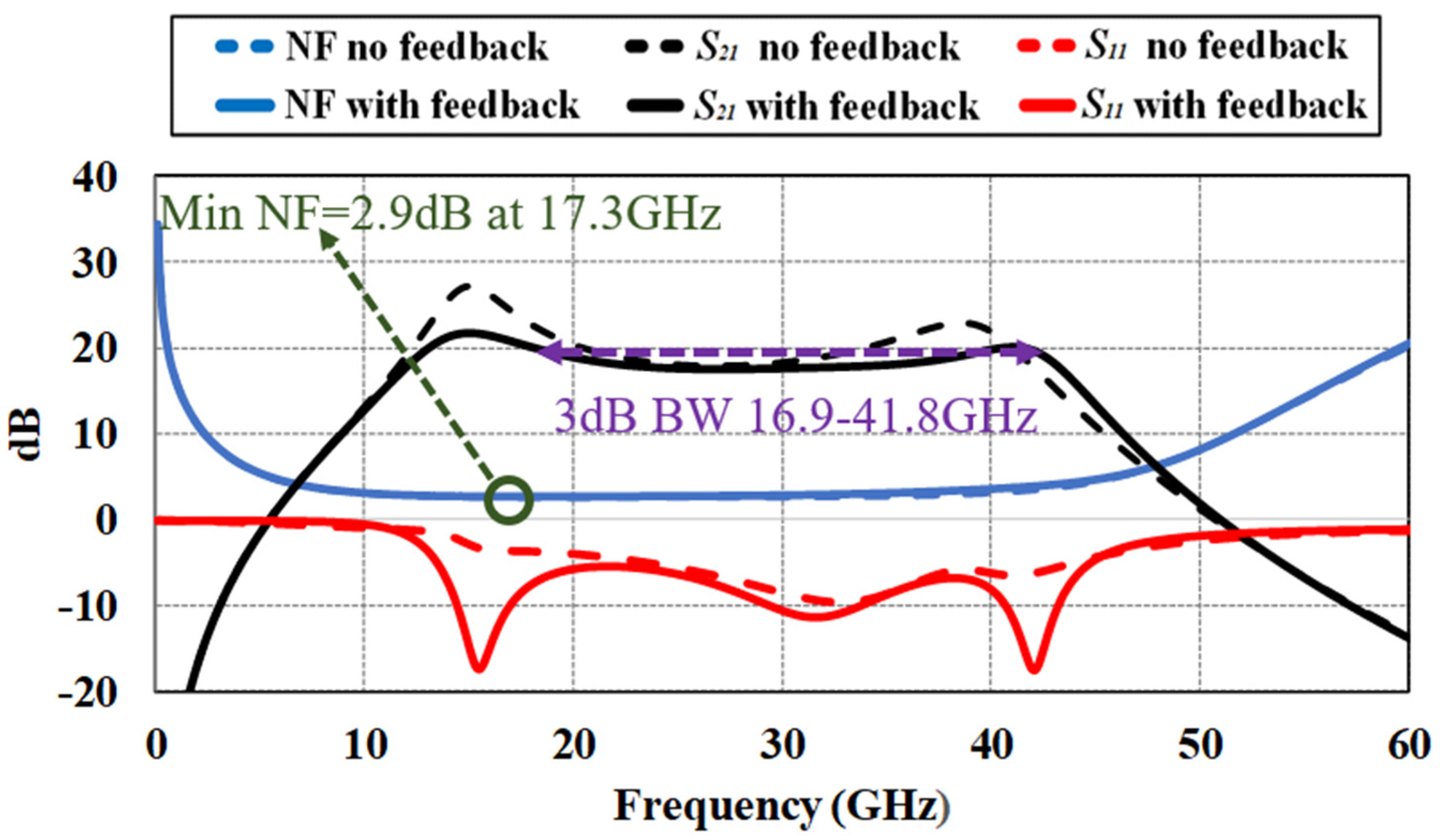
2.4. Resistive Feedback Network for Improved Input Matching and Broadband Gain Response

Equations (2)–(4) offer some key insights into the analysis of the LNA input impedance [15]. When we neglect the gate-drain capacitance of M1 in Figure 3a, the degeneration inductor L2 can supply a real impedance at the input of M1 [16]. However, it is important to note that Zin2 in Equation (3) can remain real only at a single resonant frequency [16]. To address this limitation and enhance the input matching bandwidth, we introduced a resistive feedback network (Rf and Cf) [15,17]. The stability and bandwidth of the LNA are influenced by the specific values chosen for Rf and Cf. A small Rf and large Cf give more amplifier feedback characteristics and make the input match more sensitive to the interstage matching network. The input impedances of the LNA at various nodes can be approximated as described in [15].
Z i n 1 j ω L 1 + ( Z i n 2 Z i n 3 )
Z i n 2 j ω L 2 + 1 j ω C g s 1 + g m 1 L 2 C g s 1
Z i n 3 R f + ( j ω L 4 Z i n 4 ) 1 + g m 1 g m 2 ( j ω L 4 Z i n 4 ) ( g m 2 + j ω C g s 2 ) [ ω 2 C g s 1 L 1 + L 2 + j ω g m 1 L 2 + 1 ]
where g m 1 / g m 2 and C g s 1 / C g s 2 are the transconductances and gate-source capacitance of transistors M1/M2. The other component values can be found in Figure 3a.
In Equation (4), one can see the presence of L4 and Zin4 also impacts the LNA input matching as indicated by its S11 frequency response. As suggested in [16], the inclusion of the resistive feedback component Rf can lead to a reduction in gain while enhancing the LNA’s bandwidth. This is because the gain reduction smoothens the two gain peaks, which, in effect, reduces the gain difference between the gain peaks and the gain trough. This improvement is reflected in our pre-PEX simulation results, as depicted in Figure 6, which illustrates an extended S21 3-dB gain bandwidth and input matching S11 over frequency.
While there are advantages in terms of increased BW and improved input matching, Rf can introduce more noise from the interstage matching network, and the negative feedback reduces the gain of the LNA. In pre-PEX noise circle simulations presented in Figure 7, the LNA’s lowest NF at 24 GHz is approximately 2.4 dB before adding resistive feedback to the LNA’s first stage and rises to 2.8 dB after including resistive feedback. Additionally, after the parasitics of the layout were extracted using PEX RCC, there was ~0.1 dB additional NF degradation, as shown in Figure 7c.

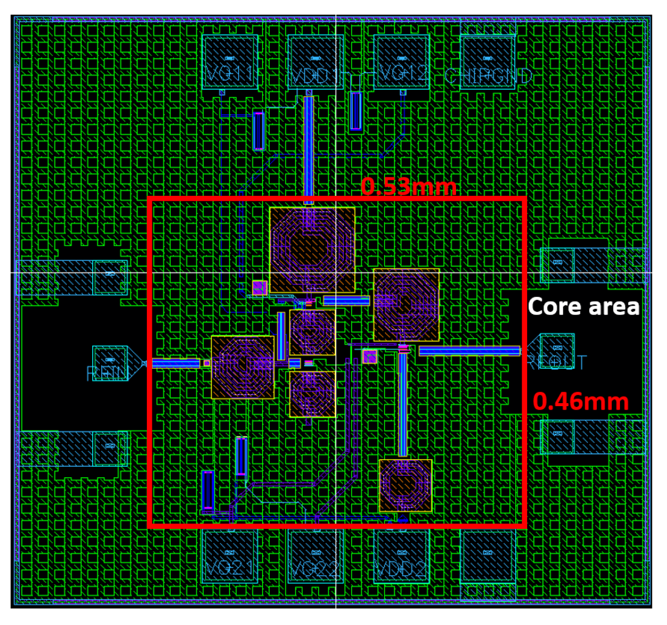
3. Layout and More PEX and EM Simulation Results

Figure 8 presents the layout of the broadband LNA, whose core size (without pads) is 0.53 × 0.46 mm2. PEX simulations were conducted using Calibre xACT v2022.2_38.20 and Cadence Spectre RF v20.1, while the EM simulations were conducted using Cadence EMX v6.3.1 (3D planar solver, Ref. [18]). The first stage operates with a supply voltage of 0.9 V, while the second stage operates at 1 V, with DC currents of 9.3 mA and 7.4 mA, respectively.

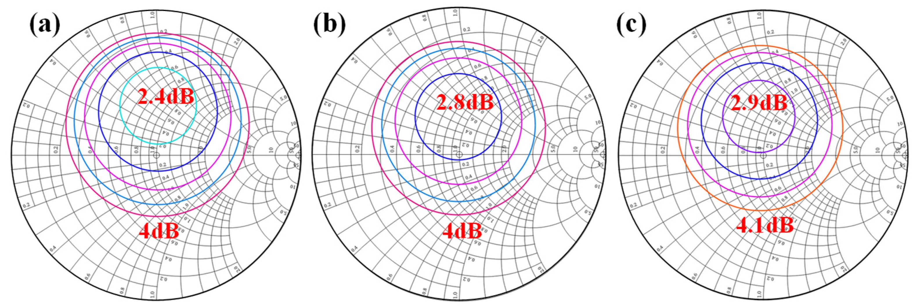
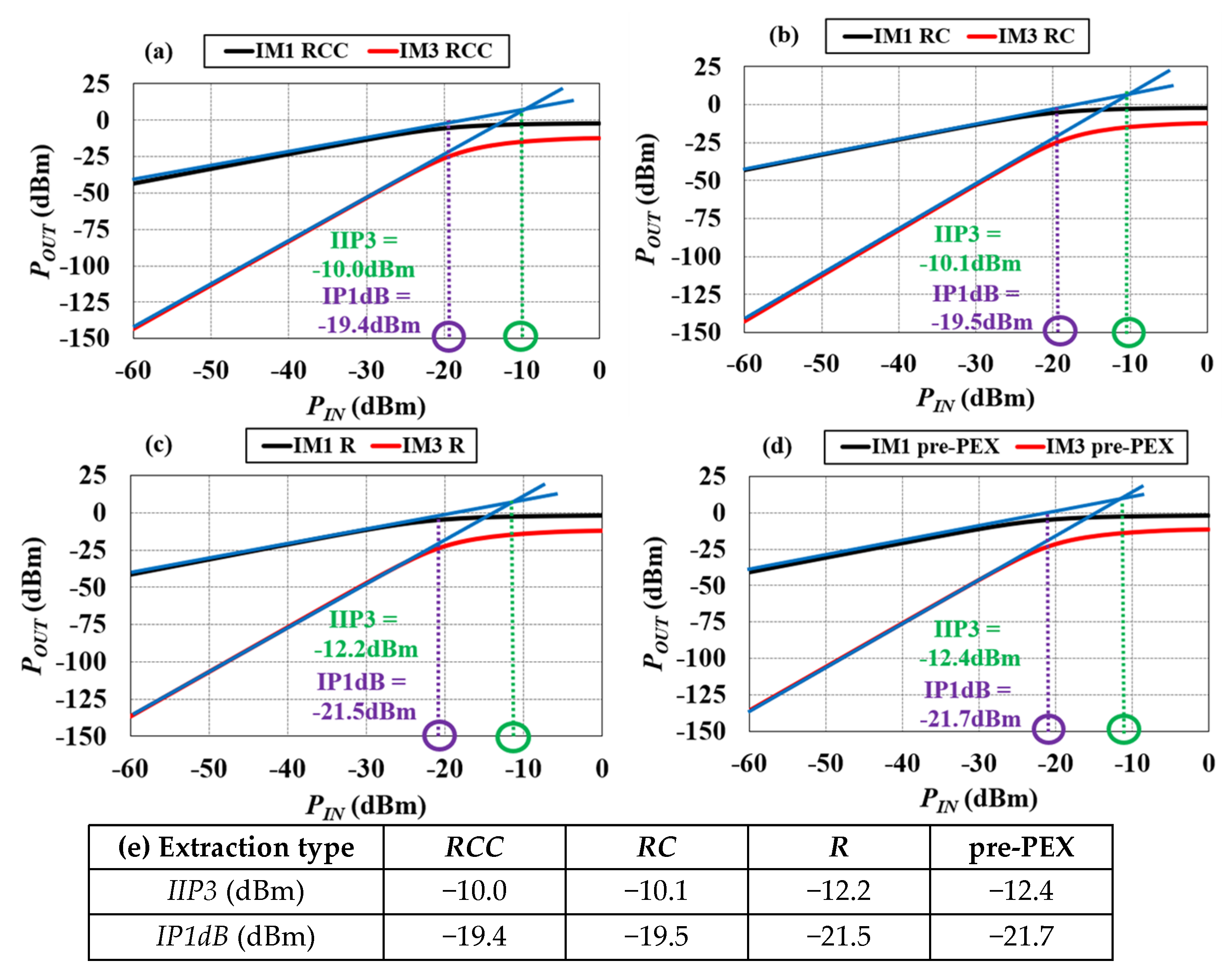
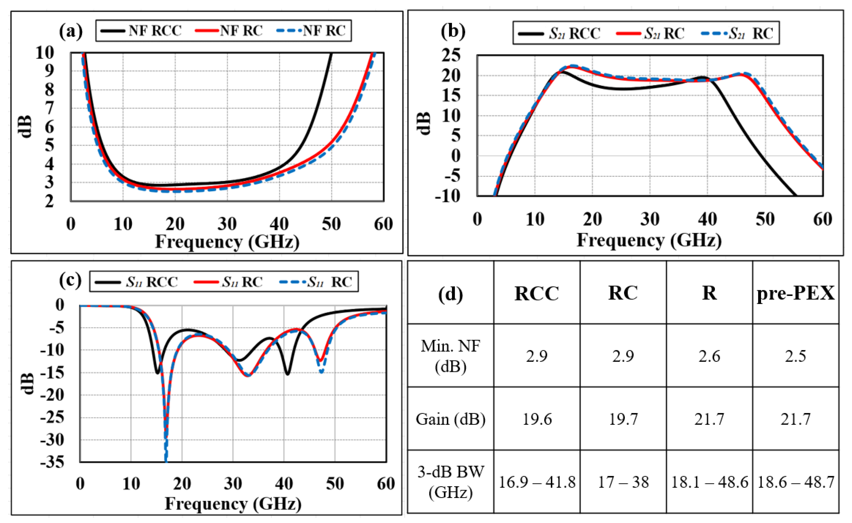
3.1. Comparison of PEX vs. Pre-PEX Simulated Results

Here, we present additional PEX simulated data using three different extraction options: R, R + C (RC), and R + C + CC (RCC). As shown in Figure 9, the performance of the LNA extracted with the RCC option exhibited the most significant degradation among the three PEX options, resulting in the poorest bandwidth, NF, and gain. This degradation can be attributed to impedance mismatches and the introduction of parasitics from the extracted layout. In other words, while the pre-PEX simulations of the LNA were originally designed to closely match the optimal gain and noise performance, the addition of extra parasitic elements caused deviations in gain and noise matching, impacting the original source/load impedance and the interstage matching. From the PEX RCC simulations, the S21 3-dB gain bandwidth ranges from 16.9 GHz to 41.8 GHz, yielding a fractional bandwidth (FBW, defined under Table 2) of 84.8%. The LNA remains unconditionally stable from these simulations (more stability analysis in Section 3.2).
The linearity of the LNA, as measured by the IP1dB and IIP3, is also compared using different PEX methods. In Figure 10, the PEX RCC simulated IP1dB is observed to be at −19.4 dBm, while the IIP3 is at −10 dBm, both simulated at 28 GHz. IIP3 was determined through a 2-tone test with a 10 MHz frequency separation. It is worth noting that both IP1dB and IIP3 are extrapolated from a Pin (input power) of −60 dBm, which falls well within the small signal region, as shown in Figure 10. The PEX RCC simulations demonstrate approximately 2 dB better performance in terms of IP1dB and IIP3 compared to the pre-PEX simulations. This improvement is likely due to the approximately 2 dB lower gain, which suggests that the OP1dB (output-referred 1 dB compression point) and OIP3 (output-referred third-order intercept point) are being compressed at nearly the same levels across all cases.

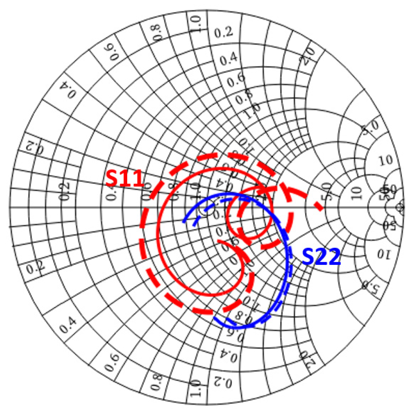
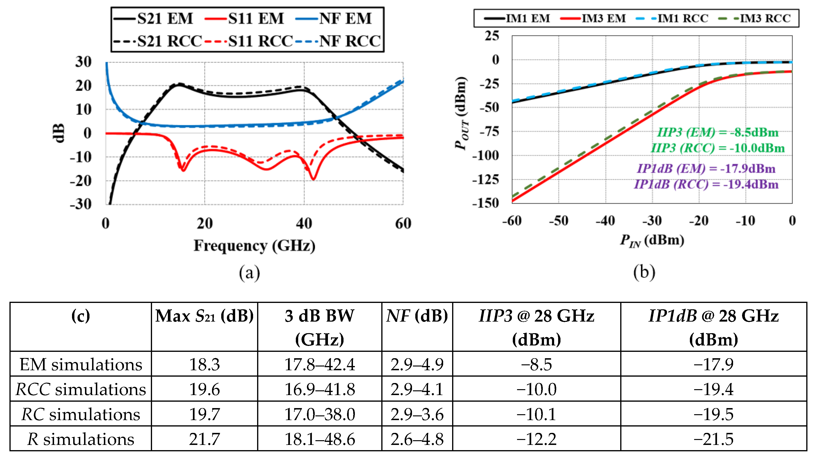
3.2. EM Simulated Results vs. PEX RCC

EM simulations usually can capture more accurately the parasitics included in the layout, but they are known to be time consuming and may not easily show the parasitics values at sensitive nodes to gain design/layout insights. Figure 11 shows the EM PEX simulation results of the LNA and compares them to the previously presented PEX RCC, RC, and R simulated data. We also observe that when gain degrades, both IP1dB and IIP3 increase. EM PEX simulated results also match closely with those from the PEX RCC simulations [12], except that the S21 bandwidth shifted by ~1 GHz toward higher frequencies, with deterioration on NF toward higher mm-Wave frequencies compared to those from the PEX RCC simulations. There is, however, a small improvement in input matching from EM PEX simulation compared to the PEX RCC simulations, as indicated in Figure 11a and Figure 12.
If we looked closely at Figure 12, we would see that the simulated S22 matches more closely between EM simulations and PEX RCC simulations than S11, likely meaning that the layout parasitics affect the load impedance more than the source impedance of the LNA. This resembles the simulation results that we saw in Section 3.1, which delineated how IIP3 and OIP3 vary with the different PEX extraction options. As the load impedance of the second stage cascode significantly influences the linearity of the LNA, if the load impedance did not vary much with the extraction option, the linearity (i.e., OIP3 and OP1dB) would not change significantly either. Having similar S22 curves suggests that the load impedance did not vary much with different extraction options. Therefore, the OIP3 and OP1dB should be similar for the PEX RCC vs. EM simulations. From Figure 10, we see that there is a 1.3 dB drop in gain in EM simulations compared to PEX RCC simulations. However, as the IIP3 and IP1dB are both ~1.5 dB higher in EM simulations, the OIP3 and OP1dB are nearly identical, similar to what we described in Section 3.1. On the other hand, S11 varies more between the two extraction options. This discrepancy may be caused by PEX RCC’s lack of inductance extraction, which may be magnified when the interconnects between the passive and active devices are longer. Since the EM results give better input matching, the input match may be improved by tuning the inductances at the input or at the interstage matching. It is also observed that the S11 locus on the Smith Chart from EM simulations is significantly shorter than the PEX RCC simulation over the same frequency range. This may mean the EM simulations incorporate more parasitic resistance during extraction, lowering the quality factor (Q factor) of the input matching network and causing the impedance to vary less with frequency. These resistances in the RF line may, in part, contribute to EM simulation’s lower gain than that from PEX RCC simulations, on top of the contributions from impedance mismatches.
Stability is one of the concerns in high-gain amplifiers and when a feedback loop is present in the circuit. Before shunt resistor R2 (see Figure 3a) was added to the output matching network, PEX RCC simulations show that both the K factor and the Mu factor are greater than 1 for all frequencies, meaning the LNA is unconditionally stable [1,2,3,5]. Here, stability factors K and Mu are defined in [19] as
K = 1 S 11 2 S 22 2 + Δ 2 2 S 12 S 21
M u = 1 S 11 2 S 22 Δ S 11 + S 12 S 21
where S 11 is the complex conjugate of S 11 and Δ = S 11 S 22 S 12 S 21 .
On the contrary, EM simulations show that at frequencies below 36 MHz, the LNA is only conditionally stable and could potentially oscillate at low frequencies. However, even though Mu is less than 1 in EM simulations, it is extremely close to 1 (only ~ 2   ×   10 6 less than 1), which means that shunting a large resistor at the output may offset the negative resistance and stabilize the circuit. As expected, when an 8.2 kΩ shunt resistor (R2 in Figure 3a) to ground was added at the LNA load, the instability disappeared at low frequencies (<100 MHz), as in Figure 13. The shunt resistor has negligible effects on the performance of the LNA, with ~0.03 dB drop in gain and virtually no change in noise figure and S11. This is primarily a result of the large shunt resistance value; for noise figure and S11, the good isolation (maximum S12 = −42.2 dB from 100 MHz to 100 GHz) in two-stage amplifiers makes these two parameters even less sensitive to the change in the LNA’s load.

4. Conclusions

This paper presents a broadband LNA design in 22 nm FD-SOI CMOS using bandwidth extension techniques to improve input matching and wide gain bandwidth. We developed a two-stage gain compensation technique by first adjusting the frequency separation and magnitude of the gain peaks in the interstage resonator, followed by using the second stage’s gain to supplement the gain droop of the first stage at midband frequencies to cover the key 5G FR2 bands. Resistive feedback was added to the first stage to smoothen the gain peaks at the first stage for improved S21- bandwidth and to address the problem of narrowband input matching in a conventional cascode LNA with inductive degeneration. The lumped-element-based PEX simulations show the parasitic effects on BW, NF and linearity from different extraction options (R, RC or RCC). PEX RCC simulations show rather similar results to the full EM PEX simulations but with significantly reduced simulation time. EM PEX simulated data suggest that the S21 3 dB BW is 17.8–42.4 GHz, with the lowest NF = 2.9 dB, a maximum small signal gain of 18.3 dB, IP1dB of −17.9 dBm and IIP3 of −8.5 dBm. Table 2 summarizes our LNA from its EM and PEX RCC simulation results and compares them with state-of-the-art mm-Wave and/or Ka-band broadband LNAs. We achieved our initial target specifications, including the S21 3-dB BW, NF and IIP3. Our design has obtained one of the highest 3 dB small signal gain bandwidths and fractional bandwidth percentages and a competitive FOM amongst the best in the literature. However, measurement data are needed to validate the PEX simulation data presented. Future endeavors include tuning the EM simulated results as suggested in Section 3.2, as well as applying some well-established linearization techniques such as feedforward or the derivative superposition method [20] to improve IIP3.

Author Contributions

Conceptualization: L.-W.O. and D.Y.C.L.; methodology: L.-W.O. and D.Y.C.L.; validation: L.-W.O., J.C.M. and C.S.; formal analysis: L.-W.O. and D.Y.C.L.; investigation: L.-W.O. and D.Y.C.L.; resources: D.Y.C.L. and J.L.; data curation: L.-W.O.; writing—original draft preparation: L.-W.O.; writing—review and editing: L.-W.O. and D.Y.C.L.; supervision: J.C.M. and D.Y.C.L.; funding acquisition, D.Y.C.L. All authors have read and agreed to the published version of the manuscript.

Funding

This research received no external funding.

Institutional Review Board Statement

Not applicable.

Informed Consent Statement

Not applicable.

Data Availability Statement

The original contributions presented in the study are included in the article, further inquiries can be directed to the corresponding author.

Acknowledgments

The authors would like to sincerely thank the excellent GF University Program and all the great support from the GF team. We are deeply indebted to the TTU Keh-Shew Lu Regents Chair Endowment Fund. We also thank the customer support from Siemens Calibre and Cadence EMX.

Conflicts of Interest

Author Jerry Lopez was employed by the company NoiseFigure Research Inc. The remaining authors declare that the research was conducted in the absence of any commercial or financial relationships that could be construed as a potential conflict of interest.

References

  1. El-Aassar, O.; Rebeiz, G.M. Design of Low-Power Sub-2.4 dB Mean NF 5G LNAs Using Forward Body Bias in 22 nm FDSOI. IEEE Trans. Microw. Theory Tech. 2020, 68, 4445–4454. [Google Scholar] [CrossRef]
  2. Hu, Y.; Chi, T. A 27–46-GHz Low-Noise Amplifier with Dual-Resonant Input Matching and a Transformer-Based Broadband Output Network. IEEE Microw. Wirel. Compon. Lett. 2021, 31, 725–728. [Google Scholar] [CrossRef]
  3. Wang, R.; Li, C.; Zhang, J.; Yin, S.; Zhu, W.; Wang, Y. A 18–44 GHz Low Noise Amplifier with Input Matching and Bandwidth Extension Techniques. IEEE Microw. Wirel. Compon. Lett. 2022, 32, 1083–1086. [Google Scholar] [CrossRef]
  4. Gao, L.; Rebeiz, G.M. A 24-43 GHz LNA with 3.1-3.7 dB Noise Figure and Embedded 3-Pole Elliptic High-Pass Response for 5G Applications in 22 nm FDSOI. In Proceedings of the 2019 IEEE Radio Frequency Integrated Circuits Symposium (RFIC), Boston, MA, USA, 2–4 June 2019; pp. 239–242. [Google Scholar]
  5. Cui, B.; Long, J.R. A 1.7-dB Minimum NF, 22–32-GHz Low-Noise Feedback Amplifier with Multistage Noise Matching in 22-nm FD-SOI CMOS. IEEE J. Solid State Circuits 2020, 55, 1239–1248. [Google Scholar] [CrossRef]
  6. Radpour, M.; Belostotski, L. An LNA with Input Power Match from 6.1 to 38.6 GHz, the Noise-Figure Minimum of 1.9 dB, and Employing Back Gate for Matching. In Proceedings of the 2022 IEEE Radio Frequency Integrated Circuits Symposium (RFIC), Denver, CO, USA, 19 June 2022; pp. 235–238. [Google Scholar]
  7. Zhang, C.; Zhang, F.; Syed, S.; Otto, M.; Bellaouar, A. A Low Noise Figure 28GHz LNA in 22nm FDSOI Technology. In Proceedings of the 2019 IEEE Radio Frequency Integrated Circuits Symposium (RFIC), Boston, MA, USA, 2–4 June 2019; pp. 207–210. [Google Scholar]
  8. Razavi, B. RF Microelectronics, 2nd ed.; Prentice-Hall: New York, NY, USA, 2012; pp. 58–60. [Google Scholar]
  9. Chauhan, V.; Floyd, B. A 24–44 GHz UWB LNA for 5G Cellular Frequency Bands. In Proceedings of the 2018 11th Global Symposium on Millimeter Waves (GSMM), Boulder, CO, USA, 22–24 May 2018; pp. 1–3. [Google Scholar]
  10. Lie, D.Y.C.; Mayeda, J.C.; Lopez, J. RF Hardware Design for 5G mm-Wave and 6G Revolutions: Challenges and Opportunities. In Proceedings of the 8th IEEE International Conference on Consumer Electronics (ICCE-TW), Penghu, Taiwan, 15–17 September 2021. [Google Scholar]
  11. Ong, S.N.; Lehmann, S.; Chow, W.H.; Zhang, C.; Schippel, C.; Chan, L.H.K.; Andee, Y.; Hauschildt, M.; Tan, K.K.S.; Watts, J.; et al. A 22nm FDSOI Technology Optimized for RF/mmWave Applications. In Proceedings of the 2018 IEEE Radio Frequency Integrated Circuits Symposium (RFIC), Philadelphia, PA, USA, 10–12 June 2018; pp. 72–75. [Google Scholar]
  12. Mayeda, J.C.; Lie, D.Y.C.; Lopez, J. Design of Broadband Highly Efficient Linear Power Amplifiers for mm-Wave 5G in 22nm FDSOI and 40 nm GaN/SiC. Electronics 2022, 11, 683. [Google Scholar] [CrossRef]
  13. Mayeda, J.C.; Tsay, J.; Lie, D.Y.C.; Lopez, J. Effective AM-PM Cancellation with Body Bias for 5G CMOS Power Amplifier Design in 22nm FD-SOI. In Proceedings of the 2019 IEEE International Symposium on Circuits and Systems (ISCAS), Sapporo, Japan, 26–29 May 2019; pp. 1–4. [Google Scholar]
  14. Kane, O.; Lucci, L.; Scheiblin, P.; Lepilliet, S.; Danneville, F. RF characterization and small signal extraction on 22 nm CMOS fully-depleted SOI technology. In Proceedings of the 2019 Joint International EUROSOI Workshop and International Conference on Ultimate Integration on Silicon (EUROSOI-ULIS), Grenoble, France, 1–3 April 2019; pp. 1–4. [Google Scholar]
  15. Wang, X.; Li, Z.; Li, Z. A 1.46-1.96dB-NF 2.1-5.2-GHz Wideband Passive Balun LNA in 22-nm CMOS. IEEE Trans. Circuits Syst. II Express Briefs 2023, 70, 3378–3382. [Google Scholar]
  16. Lee, T.H. The Design of CMOS Radio-Frequency Integrated Circuits, 2nd ed.; Cambridge University Press: New York, NY, USA, 2004; pp. 376–380. [Google Scholar]
  17. Kim, C.-W.; Kang, M.-S.; Anh, P.T.; Kim, H.-T.; Lee, S.-G. An Ultra-Wideband CMOS Low Noise Amplifier for 3-5GHz UWB System. IEEE J. Solid State Circuits 2005, 40, 544–547. [Google Scholar]
  18. Dunn, J.M.; Kapur, S.; Long, D. EMX: Overcoming Silicon Chip EM Simulation Challenges for Passive Circuit Analysis and Model Development. In Proceedings of the 2021 International Applied Computational Electromagnetics Society Symposium (ACES), Hamilton, ON, Canada, 1–5 August 2021; pp. 1–4. [Google Scholar]
  19. Pozar, D.M. Microwave Engineering, 4th ed.; John Wiley & Sons Inc.: Hoboken, NJ, USA, 2012; p. 567. [Google Scholar]
  20. Zhang, H.; Sánchez-Sinencio, E. Linearization Techniques for CMOS Low Noise Amplifiers: A Tutorial. IEEE Trans. Circuits Syst. I Regul. Pap. 2011, 58, 22–36. [Google Scholar] [CrossRef]
Figure 1. NMOS’s minimum noise figure as a function of frequency at various finger widths (total width = 19.2 μm).
Applsci 14 03080 g001
Figure 2. NMOS contact poly pitch (CPP).
Applsci 14 03080 g002
Figure 3. (a) Schematic of the 2-stage LNA and its passive component values (b) Load impedance of first stage cascode (Zload1) and the simplified small signal model of M3.
Applsci 14 03080 g003
Figure 4. Power gain of first, second and overall stages (pre-PEX). The first stage’s power gain was simulated from the RF input to the input of C3, while the second stage power gain was simulated from the input of C3 to the RF output.
Applsci 14 03080 g004
Figure 5. Pre-PEX simulated power gain circles (brown: 24 dB, green: 25 dB, blue: 26 dB) at (a) 24 GHz, (b) 30 GHz, and (c) 40 GHz with the load impedance locus (red trace) from 20 GHz to 40 GHz (red dots are the load impedances at their specified frequencies above the Smith Charts (i.e., 24, 20 or 40 GHz)).
Applsci 14 03080 g005
Figure 6. S21, S11 and NF comparison on our 2-stage LNA: resistive feedback vs. no resistive feedback (from pre-PEX simulations).
Applsci 14 03080 g006
Figure 7. Comparison of simulated noise circles at 24 GHz at the LNA input in 0.4 dB increments. (a) Without resistive feedback (pre-PEX). (b) With resistive feedback (pre-PEX). (c) With resistive feedback (PEX simulation using RCC extraction option; more on the extraction option in the next section).
Applsci 14 03080 g007
Figure 8. Layout of the broadband 2-stage LNA. The red box specifies the core area (0.24 mm2) of the amplifier.
Applsci 14 03080 g008
Figure 9. PEX (RCC, R) vs. pre-PEX comparison in (a) NF (b) S21 (c) S11 (d) comparison table (includes RC).
Applsci 14 03080 g009
Figure 10. Comparison of IIP3 and IP1dB at 28 GHz from PEX simulations in (a) RCC; (b) RC; (c) R; (d) pre-PEX cases; and (e) the comparison table summary.
Applsci 14 03080 g010
Figure 11. Comparison of EM simulation vs. PEX RCC in (a) S21, S11, NF and (b) IIP3 and IP1dB at 28 GHz (c) comparison table.
Applsci 14 03080 g011
Figure 12. S11 (red) and S22 (blue) of the LNA from 16 GHz to 44 GHz. EM simulation (solid line) vs. PEX RCC simulations (dashed line).
Applsci 14 03080 g012
Figure 13. K factor and Mu with (blue) vs. without (red) an 8.2 kΩ shunt resistor at the output between 1 MHz and 100 MHz in EM simulations. With an 8.2 kΩ shunt resistor, K factor and Mu are greater than 1 which means the LNA is unconditionally stable.
Applsci 14 03080 g013
Table 1. NFmin at 28 GHz and fT/fMAX of NMOS devices of various widths with CPP of 104 nm (CPP1x) or 208 nm (CPP2x). [gate voltage = 0.45 V, drain voltage = 0.9 V].
W/L8 µm/18 nm16 µm/18 nm32 µm/18 nm64 µm/18 nm
CPP1x/2x1x/2x1x/2x1x/2x
NFmin @ 28 GHz (dB)0.691/0.6360.839/0.7091.175/0.8661.926/1.168
fMAX (GHz)303/309253/273182/222139/188
fT (GHz)349/344371/372381/386386/391
Table 2. Performance summary and comparison vs. state-of-the-art broadband mm-Wave and/or Ka-band LNAs.
This Work
(EM)
This Work
(RCC)
[2]
MWCL ‘21
[3]
MWCL ‘22
[4]
RFIC ‘19
[5]
JSSC ‘20
[1]
TMTT ‘20
[6]
RFIC ‘22
[7]
RFIC ‘19
Technology22 nm FDSOI45 nm RFSOI65 nm CMOS22 nm FDSOI22 nm FDSOI22 nm FDSOI22 nm FDSOI22 nm FDSOI
Topology2-stage CAS2-stage CAS2-stage CS +
1 stage CAS
3-stage CAS1-stage CS + 1stage CAS with CS source-gate FB1-stage CS2-stage CS2-stage CAS2-stage CS + buffer1-stage CAS
S21 3 dB BW (GHz)17.8–42.416.9–41.825.5–5018–4424–4319–3620–3621.6–32.819.5–2923–276.1–26.223–40
FBW (%)81.784.864.983.956.761.857.141.239.616124.554.0
VDD (V)0.9/11.311/1.6 1.051.050.8/1.60.4/0.80.8/1.60.8/0.41.3
Max S21 (dB)18.319.621.219.52321.517.97.8/10.216.9/20.123.2/28.515.612.6
NF (dB)2.9–4.92.9–4.12.4–4.22.6–3.5
(20–43 GHz)
3.1–3.71.7–2.22.1–2.92.65/2.2 #2.18/2.08 #2.38/2.25 #1.9-2.91.35
IP1dB (dBm)−17.9
(@ 28 GHz)
−19.4
(@ 28 GHz)
−20.6 *
(@ 39 GHz)
−23 to −18.5−20.4 to −27−23 *
(@ 22 GHz)
−24 *
(@ 22 GHz)
−3
(@ 28 GHz)
−10.2
(@ 28 GHz)
−21
(@ 26 GHz)
−13
(@ 20 GHz)
−7.9
(@ 28 GHz)
IIP3 (dBm)−8.5−10.0−11.0−13.4 to −8.9 *−13.2 to −19−13.4
(@ 22 GHz)
−14.4
(@ 22 GHz)
7.5
(@ 28 GHz)
2.6
(@ 28 GHz)
−10.4
(@ 26 GHz)
−3.6
(@ 20 GHz)
1.4
(@ 28 GHz)
Power (mW)15.825.51720.517.35.66/153.2/9.65.5/207.813
Core area (mm2)0.240.380.160.210.050.050.120.190.190.030.12
FOM18.921.719.723.020.826.329.214.7/11.230.2/23.825.3/17.826.423.7
FOM = 20 × log((Gain [V/V] × S21 3dB BW [GHz])/(PDC [mW] × (F-1))) [1], where F is the noise factor; CAS: cascode; CS: common source; FBW: fractional bandwidth = 100% × (upper range frequency − lower range frequency)/center frequency; FB: feedback; * Estimated using IIP3 = IP1dB + 9.6 dB; # Mean value within 3-dB BW.
Disclaimer/Publisher’s Note: The statements, opinions and data contained in all publications are solely those of the individual author(s) and contributor(s) and not of MDPI and/or the editor(s). MDPI and/or the editor(s) disclaim responsibility for any injury to people or property resulting from any ideas, methods, instructions or products referred to in the content.

