Article

Design of a Double-Matched Cross-Polar Single Antenna Harmonic Tag

by
Alessandro DiCarlofelice
1,
Antonio DiNatale
2,
Emidio DiGiampaolo
1 and
Piero Tognolatti
1,*
1
Department of Industrial and Information Engineering and Economics, University of L’Aquila, 67100 L’Aquila, Italy
2
Thales Alenia Space Italia, 67100 L’Aquila, Italy
*
Author to whom correspondence should be addressed.
Appl. Sci. 2025, 15(8), 4590; https://doi.org/10.3390/app15084590
Submission received: 14 March 2025 / Revised: 7 April 2025 / Accepted: 14 April 2025 / Published: 21 April 2025
(This article belongs to the Section Electrical, Electronics and Communications Engineering)

Abstract

:
Radio frequency identification (RFID) technology has gained significant attention in various industry sectors due to its potential for efficient inventory management, asset tracking, and object localization. Different RFID technologies are available; resorting to harmonic signals is currently less used but, recently, has gained interest in research activity. In this study, we present the design, prototype realization, and performance evaluation of a dual-band dual-polarized harmonic tag. The tag incorporates a dual-band matching circuit utilizing a zero-bias Schottky diode HSMS-2850 connected to a perturbed annular ring patch antenna. The antenna, in fact, is able to radiate in cross-polarization at the higher frequency. Through a comprehensive design methodology, including simulation optimization and prototype fabrication, we demonstrate the successful implementation of the tag. Measurements to validate the impedance matching properties, radiation patterns, and backscattering capability of the tag are also shown.

1. Introduction

Nowadays, the need for identifying, localizing, tagging, tracking, and sensing objects is highly requested in various sectors, including healthcare, retail, logistics, and agriculture [1,2,3,4,5]. Radio frequency identification (RFID) is a widely used technology to perform the mentioned tasks. RFID systems operate across a range of frequencies, ranging from low-frequency (LF) bands to microwave ISM (Industrial, Scientific, and Medical) bands, and they are based on both active and passive configurations.
Active RFID systems are battery-powered and can achieve extensive read ranges, often exceeding 100 m and, in some cases, extending beyond 1 km [6]. On the other hand, passive RFID systems rely on harvesting energy from incoming electromagnetic (EM) fields, and their read range is constrained by their energy-harvesting capabilities [7]. Passive LF RFID is typically used for short-range communication, covering approximately 5 cm, while ultra-high-frequency (UHF) passive RFID extends the read range to about 6–8 m. The absence of batteries in passive RFID tags contributes to their compact form factor, lower cost, and ease of adoption in various applications.
Passive RFID can be categorized into two distinct groups: chipless RFID and chip-based RFID. The fundamental differentiation between these categories lies in the absence or presence of a microchip that essentially increases the capacity of the tag to store and exchange information. Chipless RFID tags, in fact, although they offer the advantages of straightforward circuit design and cost-effectiveness, are constrained by the information storage capacity (that is limited) and by the backscattering principle, which imposes limitations on their reading distance. Typically, chipless RFID tags exhibit reading distances of less than one meter, and their data storage capabilities range from a few bits to several tens of bits [8].
In contrast, chip-based RFID tags offer extended read distances, typically spanning from one to twelve meters, and they can store significantly larger amounts of data, often in the range of tens to hundreds of bits [9]. Moreover, chip-based RFID systems provide the capacity to read multiple tags simultaneously, with recent research suggesting the potential to concurrently read up to a thousand tags [9]. Additionally, chipless RFID tags generally require antennas with broader bandwidths, while chip-based RFID tags operate efficiently with narrower-band antennas [10].
The effectiveness of these systems, however, is affected by environmental conditions and, in particular, by the effect of metal structures. Numerous studies have been conducted to mitigate the influence of metallic and other materials on RFID tag performance. Lach et al. [11] investigated the deterioration in performances of UHF RFID tags, taking into account the presence of nearby objects and materials. Another study [12] focused on the surface materials used for RFID tag placement, emphasizing how the materials used for packaging in logistics environments, in conjunction with their contents, often create a complex and non-uniform environment. Furthermore, in-depth analyses of how metals within the environment affect the radiation pattern of RFID tags and, consequently, the overall characteristics of antennas have been detailed in [13,14]. It is clear from [12,13,14] that the effect of the electromagnetic interaction of the antenna with the objects close to the tag position makes tag detection difficult since various mismatch processes on the input impedance and on the radiation pattern are not at all negligible. Variations in the performance of passive UHF RFID tags under practical conditions [15] can be attributed to the interactions with objects situated within the environment. The effect of the environment has been addressed by several authors who have proposed methods and models to quantify such effects and to reduce them. In particular, ref. [16] reports special techniques to adjust antenna impedance and improve the efficiency of the tag, ref. [17] proposed a regression model of the impact of external factors acting on the readability of the RFID transponder, and ref. [18] focuses on the impact of the temperature of the environment on the readability of RFID tag, proposing a suitable mathematical model. To reduce the mismatch effect due to the tag placement on objects, it would be appropriate to provide the tag with an adequate shield (ground plane) in order to counteract the electromagnetic coupling between the tag and the object, while, to reduce the camouflage effects due to scattering from the environment, polarization diversity techniques can be used. In challenging application scenarios, harmonic tags present a valid alternative to traditional RFID systems. Simple harmonic transponders have already found utility in diverse applications, including the study of bee behavior [19] and avalanche victim rescue operations [20]. This suitability arises from the inherent robustness of harmonic systems in cluttered environments and their reliance on simple circuit architectures. Nevertheless, one limitation of harmonic systems in comparison to standard UHF RFID transponders is the necessity for transmitting and receiving antennas operating at distinct frequencies on the tag. This requirement can lead to the creation of somewhat unwieldy transponders [21]. Some research efforts have explored solutions based on dual-frequency single antennas [22,23]. These solutions predominantly rely on dipole-like antennas and, more broadly, on omni-directional radiators. When these antennas interact with the materials of the items to which the tag is affixed, they can become detuned, potentially compromising the reliability of the entire system.
To generate harmonics from an RF signal, a nonlinear device is used [24]. In the existing literature, various types of active or passive frequency multipliers, such as diodes [25,26], nonlinear transmission lines (NLTL) [27,28], transistors [29], or delayed lock loops (DLL) [30], have been suggested to achieve frequency multiplication ranging from 2× to 8×. Schottky and varactor diode-based harmonic generators are ideal from a power consumption perspective due to very minimal or almost no power consumption.
This paper presents a novel harmonic tag model based on microstrip antenna technology having dual-band dual polarization with the doubler circuit included inside the antenna. Figure 1 provides a schematic representation of the proposed design. The main novelties are as follows:
  • A new concept of a one-port harmonic transponder matched at both frequencies;
  • A new exploitation of the modal behavior of annular ring antenna that allows dual polarization using only one compact antenna;
  • The insensitivity of the tag to the object on which it will be placed (e.g., it can be wearable) thanks to the use of microstrip technology.
Compared to a dipole-like antenna, an annular ring antenna has the advantage of having a higher gain and being insensitive to where it is placed. The inclusion of dual polarization allows for better distinguishing the tag response from cross-talk phenomena between the receiving and transmitting channels of the reader.
In this work, we report a comprehensive study of the design, realization, and measurements of the harmonic tag. The tag incorporates a dual-band harmonic circuit (i.e., a single-port doubled-matched doubler) connected to an annular patch antenna specially modified to achieve both matching and orthogonal linear polarized radiation at two harmonic bands. The orthogonal polarization is a requirement used to mitigate the effect of environmental clutter. Thanks to the ground plane of the antenna, the tag has good flexibility and adaptability for a wide range of wireless sensing applications from wearable sensing to IoT applications. We design the tag to operate at 1.7 GHz and 3.4 GHz, as those bands are allocated for mobile and radiolocation in all European countries participating in the CEPT ECC (Electronic Communications Committee) [31].
The paper is organized as follows: Section 2 describes the dual-band doubler circuit, showing the used method, the constraints, and the results of its design; Section 3 reports the rationale of the dual-band, dual-polarized antenna and its design procedure; Section 4 shows the electromagnetic analysis of the whole tag structure and its simulative assessment; Section 5 reports details of prototype realization and the measurement results; Section 6 reports a discussion and conclusion.

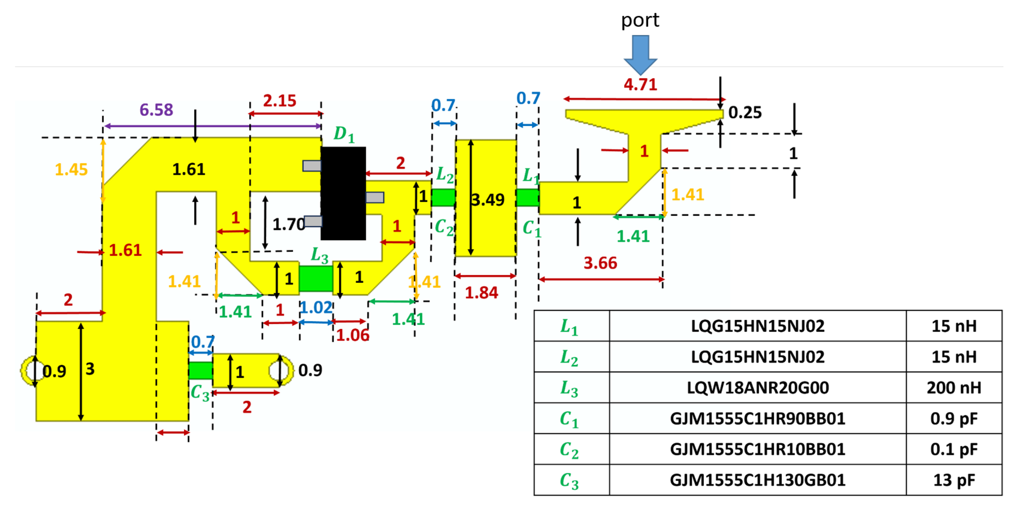
2. Doubled-Matched Doubler Circuit

In wireless sensing systems, the efficient transfer of RF energy between the antenna and the tag’s circuitry is crucial for optimal performance. To achieve this, a well-designed matching circuit is required. In this section, we focus on the design considerations and implementation of a single-port doubler that is matched at two frequencies: the fundamental and its second harmonic.
The circuit includes the used Schottky diode, inductors, and capacitors with lumped element models. Specifically, to obtain even more realistic results, the S-parameter models of the individual components (provided by the manufacturers, in our case, Murata [32]) are included in the simulator. The presence of these components significantly reduced the circuit’s size compared to a fully microstrip version [33]. This design strategy has been carried out with the aim of making the doubler circuit integrable with a small antenna to compose the tag.
The Schottky diode is a key component in the tag’s matching circuit that is responsible for the generation and extraction of harmonic frequencies. The design of a single-port doubler plays a vital role in achieving impedance matching between the antenna and the diode, ensuring maximum power transfer and effective harmonic generation. The dual-band network of the doubler circuit was first designed using AWR Microwave Office [34]. The design process considers a Teflon substrate ( ϵ r = 2.1 , tan δ = 0.0027) with a thickness of h = 1.5 mm. The selected operating frequencies is 1.7 GHz (fundamental) and its double value, 3.4 GHz (second harmonic). The layout of the final circuit, shown in Figure 2, has been obtained through a two-step optimization process. The first step is performed by means of a Harmonic Balance analysis (under AWR), taking into account the nonlinearity of the used diode. The corresponding optimization has been subjected to the following constraints: (i) the incident power level at the port of the network is set to −30 dBm since this is a reasonable level in practical applications; (ii) the reflection coefficient at the considered frequencies is set to be less than −20 dB; (iii) the conversion loss (i.e., the power difference between the input power to the circuit and the backscattered power at the second harmonic) is less than 30 dB.
In our design, we chose an HSMS-2850 zero-bias Schottky diode, well-suited to operate in a small-signal regime (Pin < −20 dBm).
Each lumped component has an effect on the behavior of the doubler circuit, and a possible variation of their value has been analyzed individually. Variations of about 10 % of the inductor L 1 cause a shift in the matching bands of the reflection coefficient (greater at first harmonic, smaller at second harmonic). A similar variation of the capacitor C 1 gives a shift in the first harmonic matching band but does not affect the second harmonic. On the contrary, a change of 10 % in inductor L 2 shifts the second harmonic but does not affect the fist harmonic matching band. Capacitor C 2 , instead, can shift both first and second harmonic matching bands for a change in its value. On the contrary, variations in the value of the capacitor C 3 do not introduce significant shifts in matching bands in the reflection coefficient but affect the length of the microstrip line connected to the cathode of the Schottky diode at the second harmonic (around 3.4 GHz). Thus, a change in these components can be compensated with a change in the length of the microstrip line during the optimization process. The 200 nH inductor ( L 3 ) placed in parallel with the Schottky diode serves to protect the diode from electrostatic discharges and DC currents; as well, it serves to set the DC working point for preventing an uncontrolled polarization of the diode that may lead to a working point with reduced nonlinearity [36].
After developing the AWR model, we performed a second optimization step based on a full-wave electromagnetic analysis, with the aim to refine the design on the basis of a more realistic model. The full-wave analysis, in fact, permits taking into account the distributed electromagnetic phenomena that may alter the functioning of the network. It has been performed with Ansys HFSS 2022R1 [37]. The S-parameter models of the various lumped circuit elements are also included in the electromagnetic simulator. A shift of approximately 100 MHz has been observed in the fundamental frequency and approximately 200 MHz in the second harmonic. To refine the design of the microstrip part of the circuit, an optimization in HFSS (Quasi-Newton algorithm) has been carried out.
The final dimensions of the doubler network layout for the HSMS-2850 diode are presented in Figure 2, while the reflection coefficient response obtained with HFSS after the final optimization is shown in Figure 3.

3. Antenna Design

An antenna that is intrinsically prepared for operating at two frequencies, approximately one double the other, is the annular ring patch antenna: it is capable of supporting both the T M 11 fundamental mode and the T M 21 mode operating at double frequency [38]. Furthermore, that antenna allows the doubler network described in the previous section to be accommodated in a compact space (the circuit can be integrated inside the ring), while it improves the wearability by means of the full ground plane on the bottom side of the antenna that shields the human body. Nevertheless, it presents a couple of drawbacks for the type of application chosen, for which it is necessary to carry out a detailed analysis in order to overcome them.

3.1. Rationale of the Antenna Design Procedure

An annular ring microstrip antenna (ARMSA) is shown in Figure 4, with r o and r i , the outer and inner radii, respectively. The resonance frequency of the ARMSA is given by [39]
f n m = c X n m 2 π r i ϵ e
where c is the speed of light, ϵ e is the effective dielectric constant, and X n m , ( n , m ) { ( N , N + ) ( 0 , 1 ) } , are the roots of a characteristic equation involving derivatives of Bessel functions. The values of X n m depend on the ratio r o r i , as well as the order n of the Bessel function and the index m of the root. An ARMSA supports a number of modes: if the ratio r o r i is not too large, X 21 is about double X 11 , so that two modes having resonant frequency, one double the other, are possible. As an example, in the case of r o r i = 2 , X 11 = 0.6773 while X 21 = 1.3406 .
Consider now Figure 4a, where the annular ring is fed by a microstrip line (to make the description easier, in the following, we name the direction of that line ‘vertical’). The mode T M 11 (Figure 4a) is characterized by a couple of surface currents that flow over the ring and are distributed symmetrically with respect to a symmetry line passing through the feeding point and the point (shown as ‘x’ in Figure 4) of the null (or minimum) magnitude of current. That current distribution allows it to radiate a linear polarized field with maximum directivity at the boresight direction (i.e., the direction orthogonal to the plane of the ring) and a beam similar to that of a half-wavelength circular patch antenna (i.e., cardioid-like), shown on the right side of Figure 4a. In T M 21 mode, currents are again symmetric with respect to the symmetry line but are anti-symmetric (i.e., 180 out of phase) with respect to the line orthogonal to the symmetry line (Figure 4b) (for simplicity, we name it anti-symmetric line). For this reason, we can identify four currents that radiate fields that are 180 out of phase with respect to the anti-symmetry line. The superposition of fields radiated by these four currents gives a null of field at the boresight direction, and the beam results are conical, as shown on the right side of Figure 4b.
Since we are interested to have similar radiation patterns at both fundamental and second harmonic frequencies, the field radiated by T M 21 mode is not suitable for our purposes. Moreover, it would be beneficial for harmonic tags to use an orthogonal polarization in replying to an interrogation, in order to mitigate the environmental clutter. Perturbation methods can be used in ARMSA to change polarization using slits or protrusions similar to stubs [38]. Figure 5 shows a schema of a possible model of perturbed ARMSA for radiating linear polarization (aligned along the anti-symmetry line) in second harmonic and preserving the maximum of directivity at the boresight direction. The feeding line is 90 rotated with respect to that of T M 11 mode (we name it ‘horizontal’), while a stub (protrusion) is connected to the ring in the opposite direction along the anti-symmetry line. At the frequency of the second harmonic, the T M 21 current distribution is preserved over the ring but an additional in-phase current is introduced over the stub (protrusion). This additional current radiates a not-null field in the boresight direction having polarization along the anti-symmetry line. The inclusion of the feeding line and the stub (protrusion) does not perturb, at the fundamental frequency, the T M 11 mode in Figure 4a since they are placed in the position where the T M 11 mode has a minimum of electric field.
Evidently, for exciting both modes T M 11 and perturbed T M 21 radiating orthogonal fields, two orthogonal feeding lines are required. Since the ARMSA has very different input impedance at the two frequencies (fundamental and second harmonic), a specific design procedure is required for fitting dimensions of feeding lines and stub (protrusion).

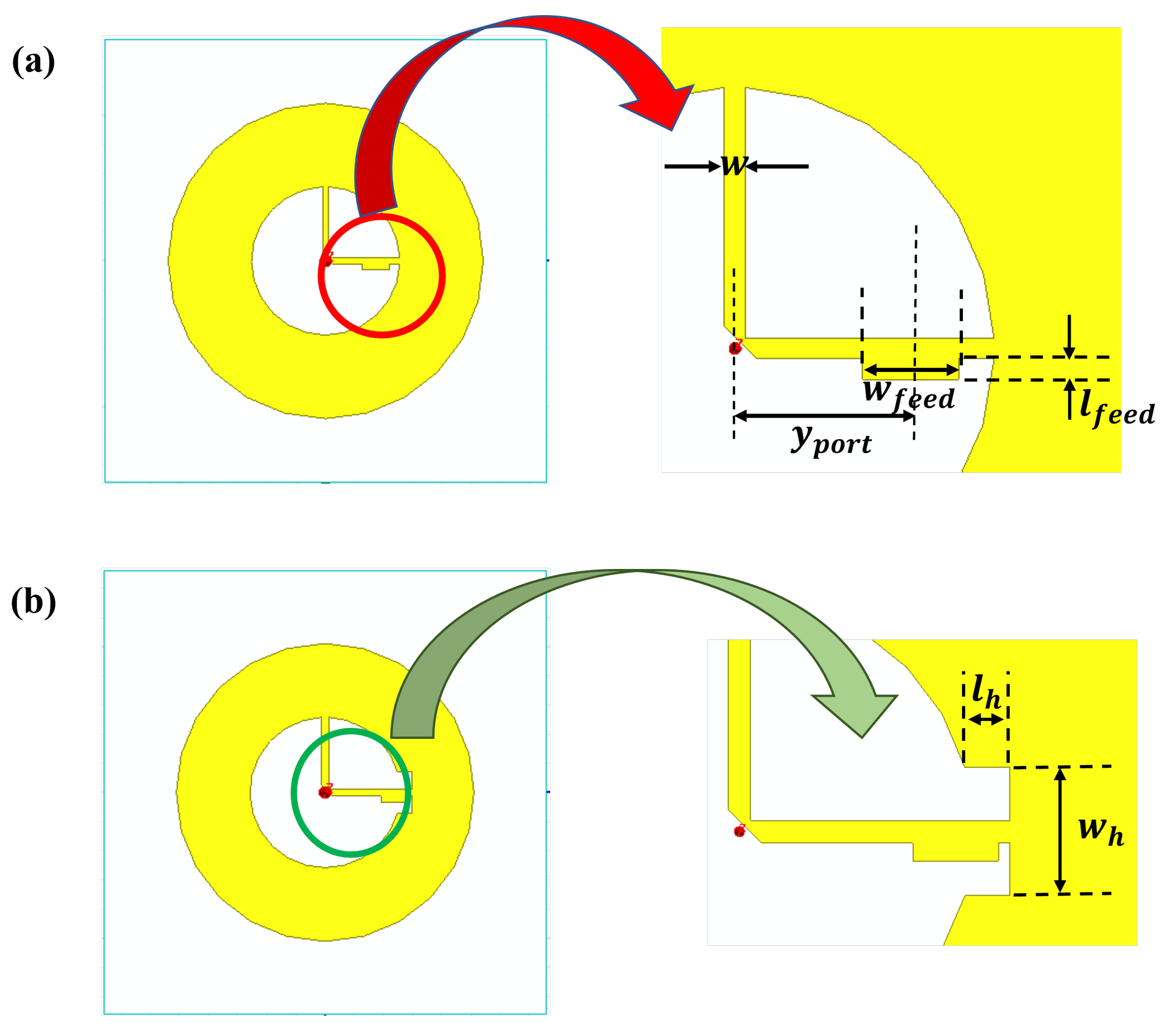
3.2. Antenna Design Procedure

The antenna structure is designed using Ansys HFSS. The substrate material is the same as previously indicated for the doubler network. The initial configuration of the antenna is shown in Figure 6, where the two feeding lines are connected together and only one port feeds the antenna (for semplicity, the adding of protusion is considered later on).
The antenna design procedure encompassed several steps. The initial one involves the dimensioning and simulation of the annular ring’s geometry [38], but it did not yield the impedance matching condition on both desired frequency bands. To achieve impedance matching at the second harmonic, a rectangular indent is added at the end of the horizontal microstrip feeding line. The application of this geometric modification, as shown in Figure 6b, facilitates the relocation of the feeding point, effectively ensuring impedance matching at 3.4 GHz. The reflection coefficient for the layouts depicted in Figure 6 is reported in Figure 7.
The use of the dual-microstrip feed permits the control of the desired relationship between the two bands. If one branch is removed or disconnected, the dual-band matching characteristic is lost.
Regarding the radiation pattern, the results obtained from the electromagnetic simulator demonstrate that, at 1.7 GHz, the typical radiation pattern of a patch antenna is observed. Nevertheless, at 3.4 GHz (second harmonic), a null of the gain is present where it would have been beneficial to have a peak ( θ = 0 , ϕ = 0 ) (see Figure 8).
To achieve a maximum radiation pattern at θ = 0 , ϕ = 0 , even at the second resonant frequency, a rectangular protrusion (like a stub) has been added to the annular ring antenna and positioned on the opposite side of the rectangular indent. This modification is illustrated in Figure 9, which also includes a circular slot whose function is explained below.
The rationale of this geometric alteration is based on altering the path of currents at 3.4 GHz in such a way to increase the radiation in the boresight direction. Also, a circular slot has been added at the crossing of the protrusion with the ring of the antenna; it is used to to make the route of the currents less intertwined at the insertion point (since the protrusion is large). Furthermore, it is beneficial to the gain that remains unchanged at 1.7 GHz while it increases by 0.5 dB at 3.4 GHz; instead, the polarizations at the two resonances are linear and orthogonal to each other. The final dimensions of the antenna with the protrusion and slot are obtained through an optimization process using HFSS electromagnetic simulator, with the primary objective of maintaining dual-band matching at 1.7 GHz and 3.4 GHz (see Table 1).
The results obtained from the simulator are presented in Figure 10, Figure 11 and Figure 12. The gains are 5.0 dBi and 6.0 dBi at 1.7 GHz and 3.4 GHz, respectively. The corresponding efficiencies are −1.4 dB and −0.4 dB. As observed, the radiation pattern at 3.4 GHz now exhibits a peak at θ = 0 , ϕ = 0 . The addition of the protrusion has also contributed to providing the antenna with the characteristic of linear polarization along the θ component at 1.7 GHz and linear polarization along the ϕ component at 3.4 GHz. This is an important feature because it allows the tag to respond in a cross-polar manner at the second harmonic with respect to the interrogation signal. Figure 12 shows surface currents flowing on the surface of the annular patch at 1.7 GHz (a) and at 3.4 GHz (b). The flow of currents agrees well with the theoretical one. In particular, inside the protrusion, the currents have opposite direction at 1.7 GHz so that they do not contribute to the V-polarized radiation; instead, they have the same direction at 3.4 GHz and contribute to the H-polarized radiated field in the boresight direction.

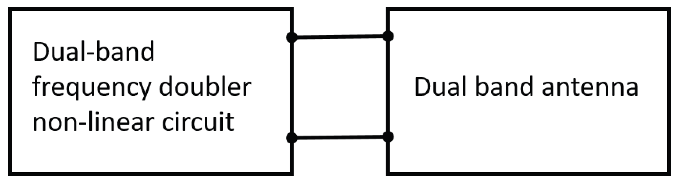
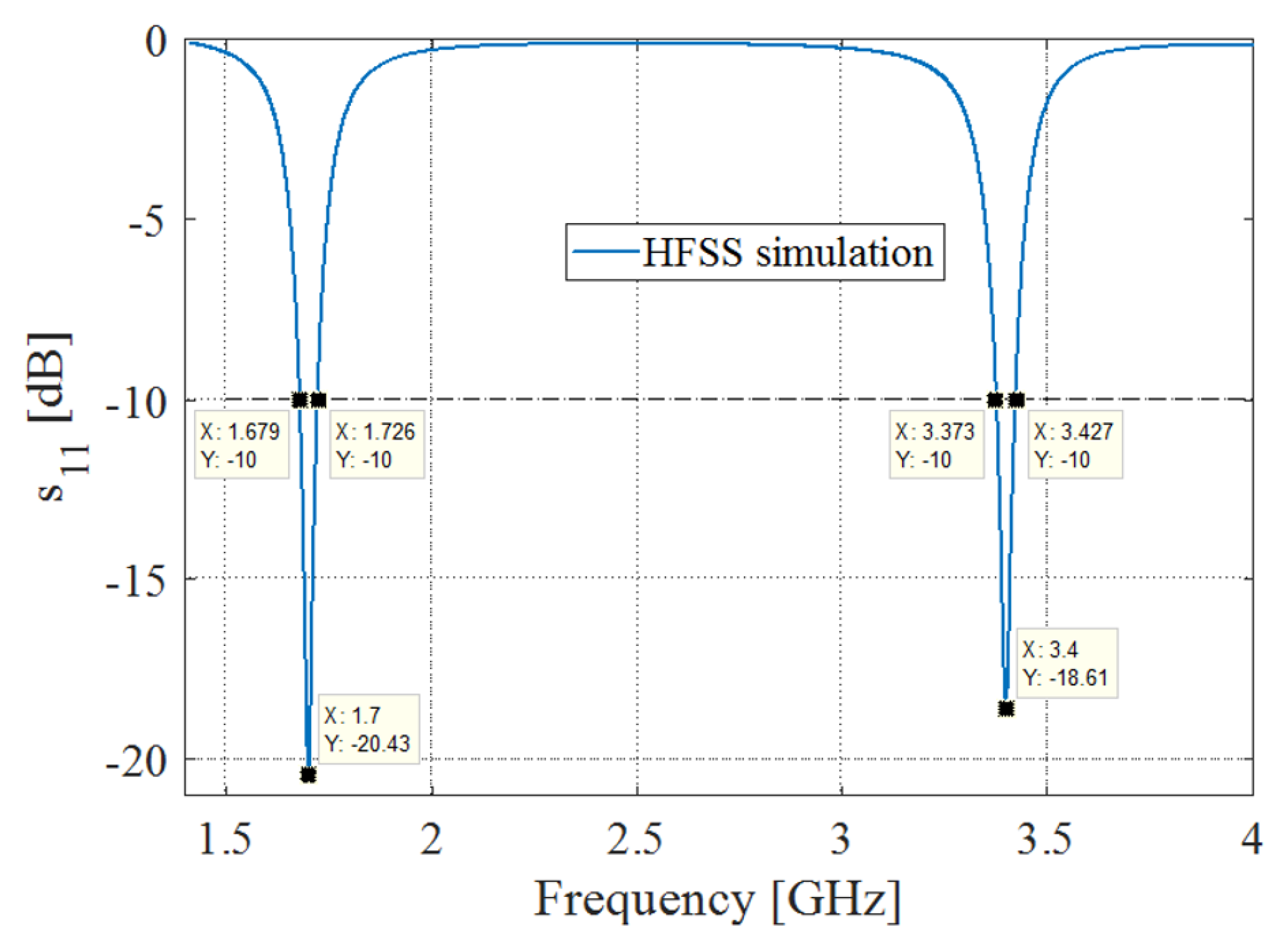
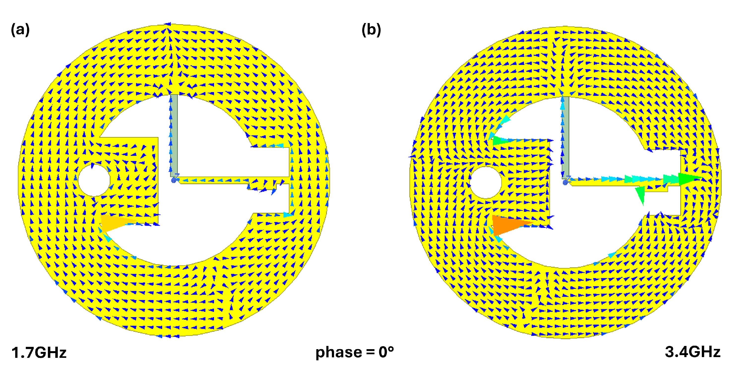
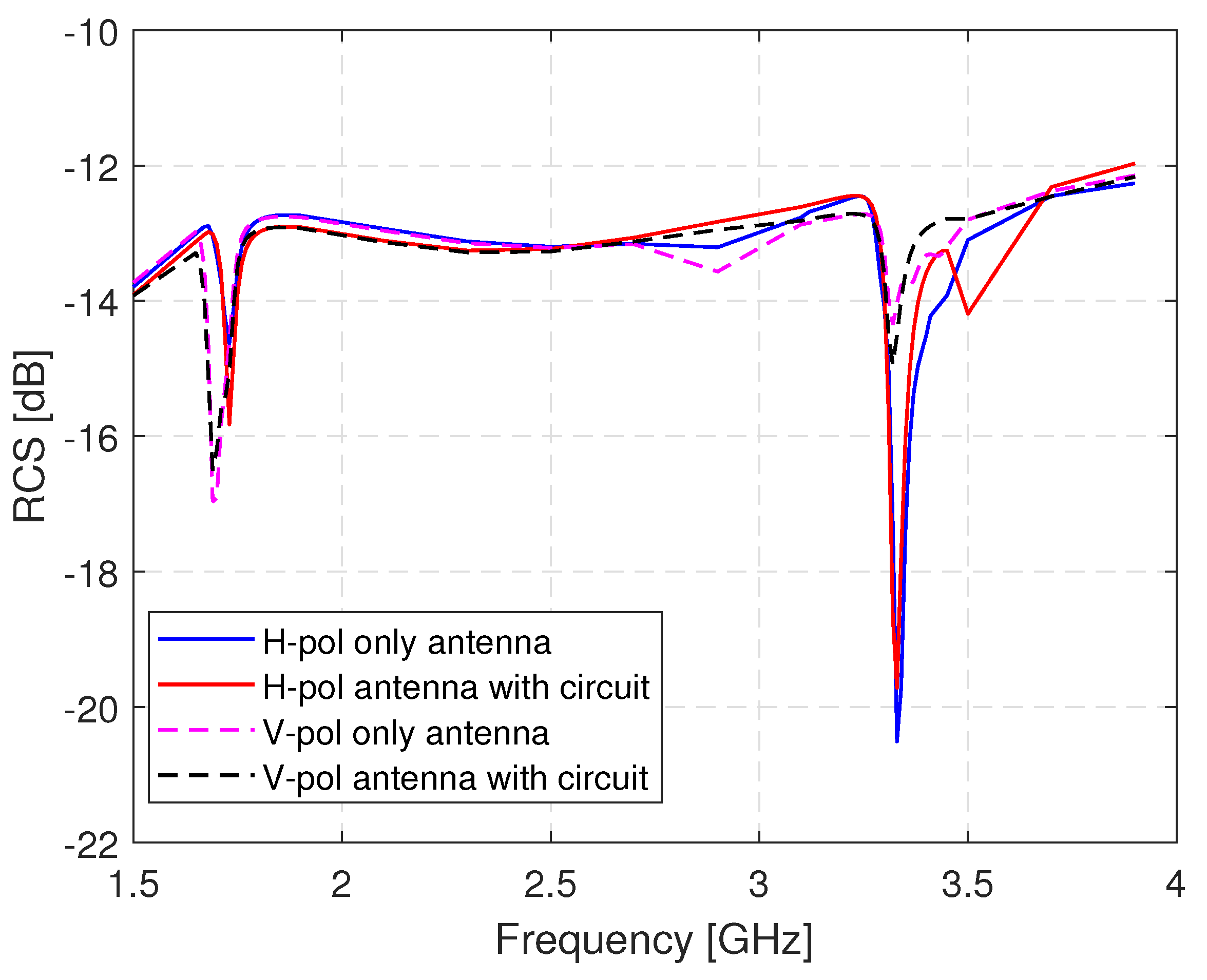
4. Electromagnetic Analysis of Assembled Doubler Network and Antenna

We proceed to analyze the electromagnetic performance of the harmonic tag as a whole by assembling the doubler network and the antenna. This involves simulating the combined effect of the doubler circuit integrated within the annular antenna layout using Ansys HFSS. The primary objective of this analysis is to examine the impact of this integration on the behavior of the tag at the two resonant frequencies, 1.7 GHz and 3.4 GHz.
For this purpose, we calculate the monostatic Radar Cross-Section (RCS) of the tag at the two considered frequencies. To analyze the effect of the coupling between the doubler circuit and the antenna, we compare the RCS obtained when the doubler circuit is integrated inside the antenna with the RCS computed by terminating the antenna port on a load that incorporates the frequency-dependent scattering parameters of the doubler circuit alone. This approach allows us to isolate the impact of the circuit integration on the antenna’s scattering properties. The simulation is performed in Ansys HFSS, modeling a pair of plane waves impinging on the tag from the boresight direction with linearly polarized electric fields, one vertically and one horizontally polarized.
The results, shown in Figure 13, compare the RCS of the assembled tag with that of the antenna alone. A strong agreement between the two cases indicates that integrating the doubler circuit inside the antenna does not significantly alter its electromagnetic behavior. In the vertical polarization case (dotted lines), the RCS exhibits a deep notch at 1.7 GHz, corresponding to the resonance of the antenna operating in the T M 11 mode. A smaller notch at 3.4 GHz is mainly due to the matching condition between the antenna and the doubler circuit at that frequency. Conversely, in the horizontal polarization case (solid lines), the deep notch occurs at 3.4 GHz, corresponding to the resonance of the T M 21 mode, while the smaller notch at 1.7 GHz is again influenced by the matching conditions between the antenna and the doubler circuit.
The presence of these deep notches confirms that the antenna efficiently absorbs incident radiation at the corresponding frequencies. This result demonstrates that the tag effectively receives a vertically polarized plane wave at 1.7 GHz and backscatters a horizontally polarized wave at 3.4 GHz, ensuring the intended harmonic response.

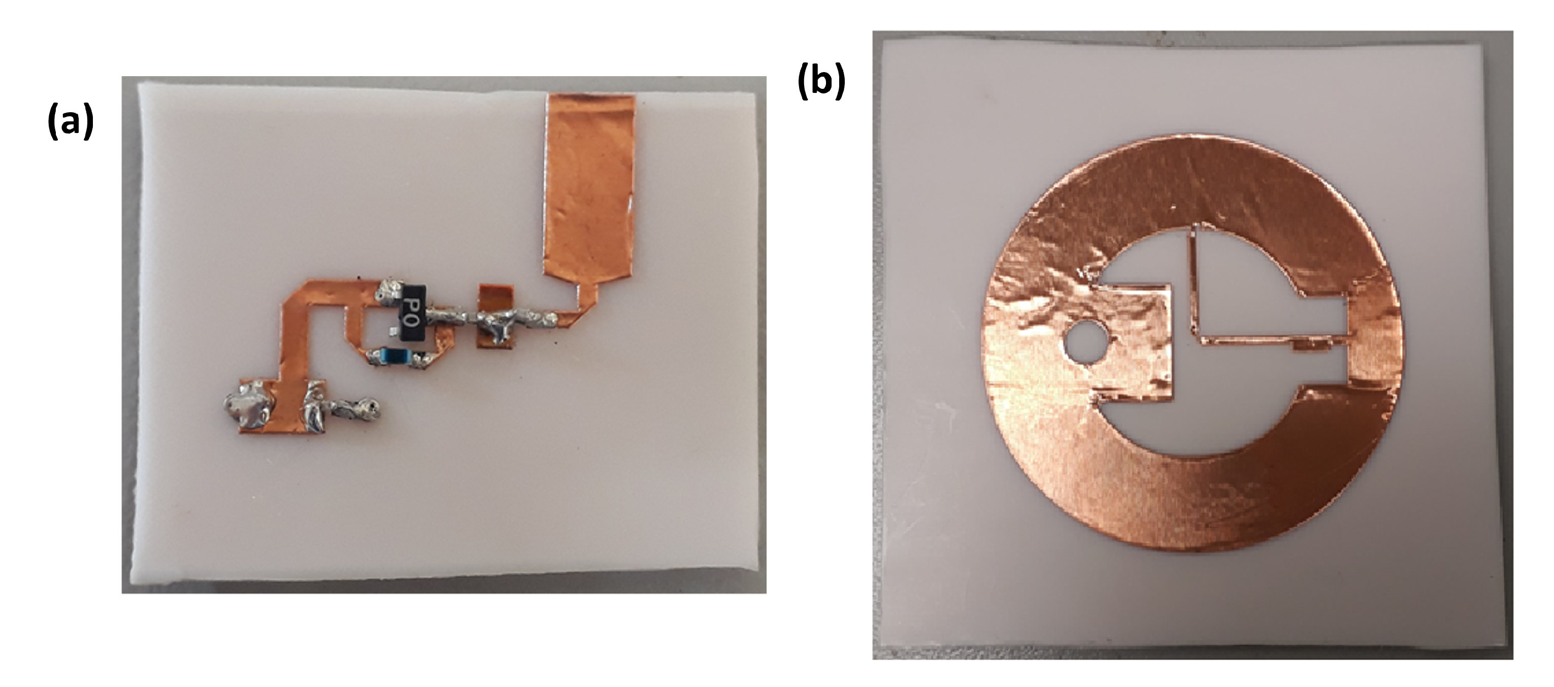
5. Prototype Realization and Measurements

For realizing a prototype of the designed harmonic tag, we use a substrate made of Teflon, which has ϵ r = 2.1 , t a n δ = 0.0027 , and thickness h = 1.5 mm. The different metallic components that constitute the circuit and the antenna (microstrips, patches, and ground planes) are made with 35 μ m thick adhesive copper. The layouts for metallic components are realized using the Secabo C60 IV cutting plotter. Photos of the prototypes can be seen in Figure 14. Inductors, capacitors, and the Schottky diode (HSMS-2850) are soldered using traditional tin alloy soldering. Prototypes of the dual-band matching circuit and the final annular antenna are realized separately in order to check their behavior separately before the final assembly (Figure 14a,b).

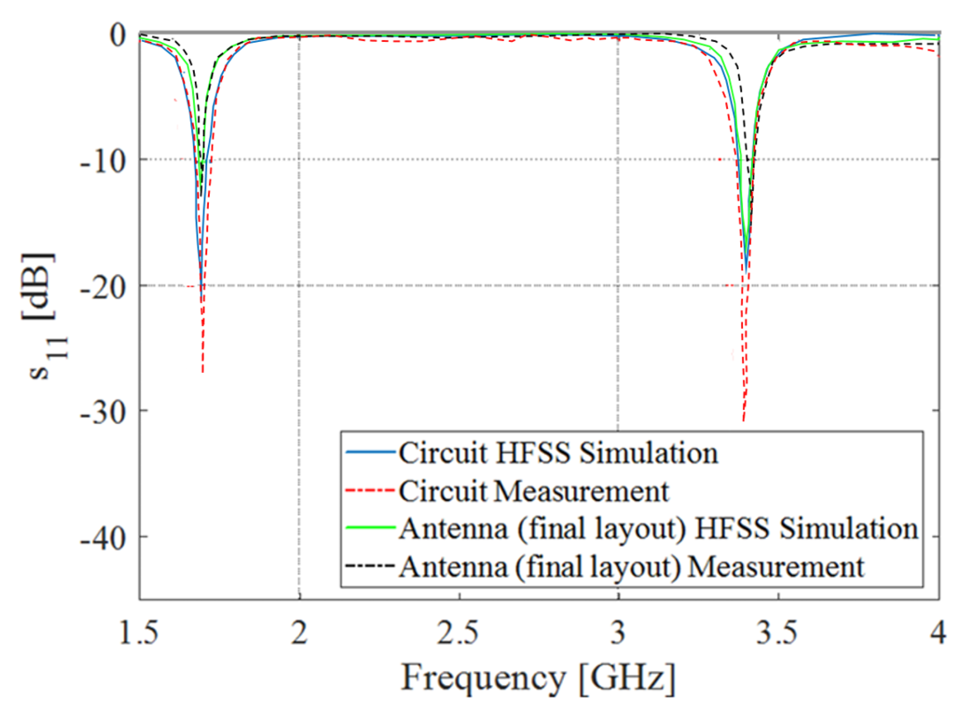
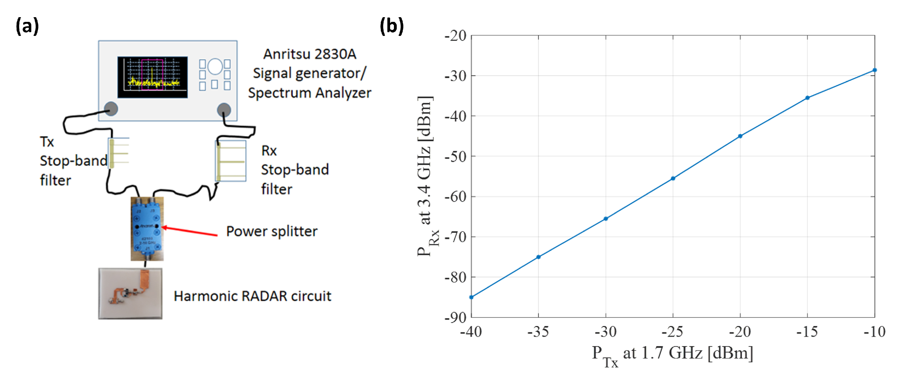
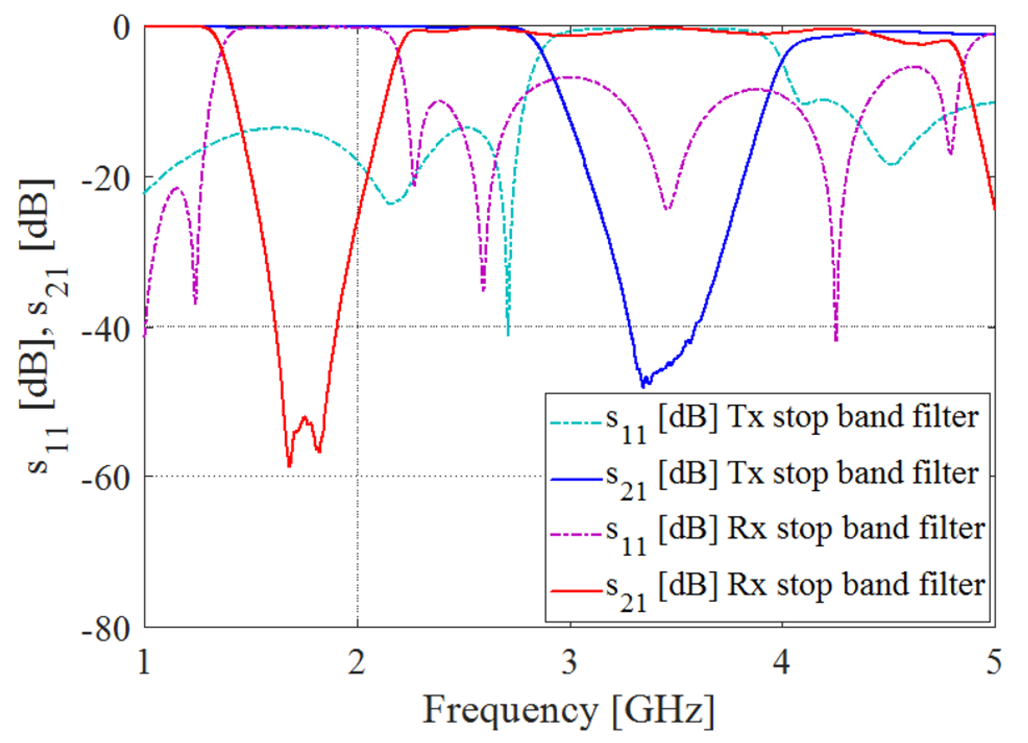
5.1. Measurements of the Realized Doubler Circuit

The reflection coefficient of the doubler circuit is carried out using the Anritsu MS46122B vector network analyzer. A 30 dB attenuator has been placed between the VNA and the port of the circuit. This setup allowed for the measurement of the circuit’s behavior under conditions similar to those assumed during simulation (i.e., with input power of −30 dBm). In fact, the nonlinear behavior of the Schottky diode makes its impedance change with the variation of the input power. The comparison between the measured reflection coefficient and the simulated one is presented in Figure 15, which also shows reflection coefficients of the antenna. As evident, measurements agree with simulations: both bands at 1.7 GHz and at 3.4 GHz have a reflection coefficient lower than −10 dB. The measured reflection coefficient of the circuit appears a little bit better than that of the simulated model likely because the prototype has losses greater than that of the model.
In order to asses the capabilities in re-transmitting the second harmonic, a continuous wave (CW) signal at a specific frequency has been sent to the input port of the doubler circuit and the power returned in the second harmonic is measured. To achieve this, the circuit has been connected to the Anritsu MS2830A signal generator/spectrum analyzer using two band-reject filters and the Anaren 42,100 power splitter. The transmission filter is inserted to further attenuate the second harmonic of the transmitter while the receiving filter was added to prevent receiver saturation at the frequency of the first harmonic. The setup is sketched in Figure 16a. Figure 17 presents the measured reflection and transmission coefficients of the two band-reject filters used in this measurement. A CW signal at 1.7 GHz is transmitted with a variable power to the doubler circuit while the power received at 3.4 GHz is measured. Figure 16b displays the measurement results, after removing the losses introduced by various components in the system (cables, filters, power splitter). That measurement permits us to retrieve the conversion loss of the circuit, which is variable with the input power—in fact, it is lower for high input power and higher for low input power (e.g., the conversion loss is about 18 dB for P T x = 10 dBm while it is 35 dB for P T x = 30 dBm).

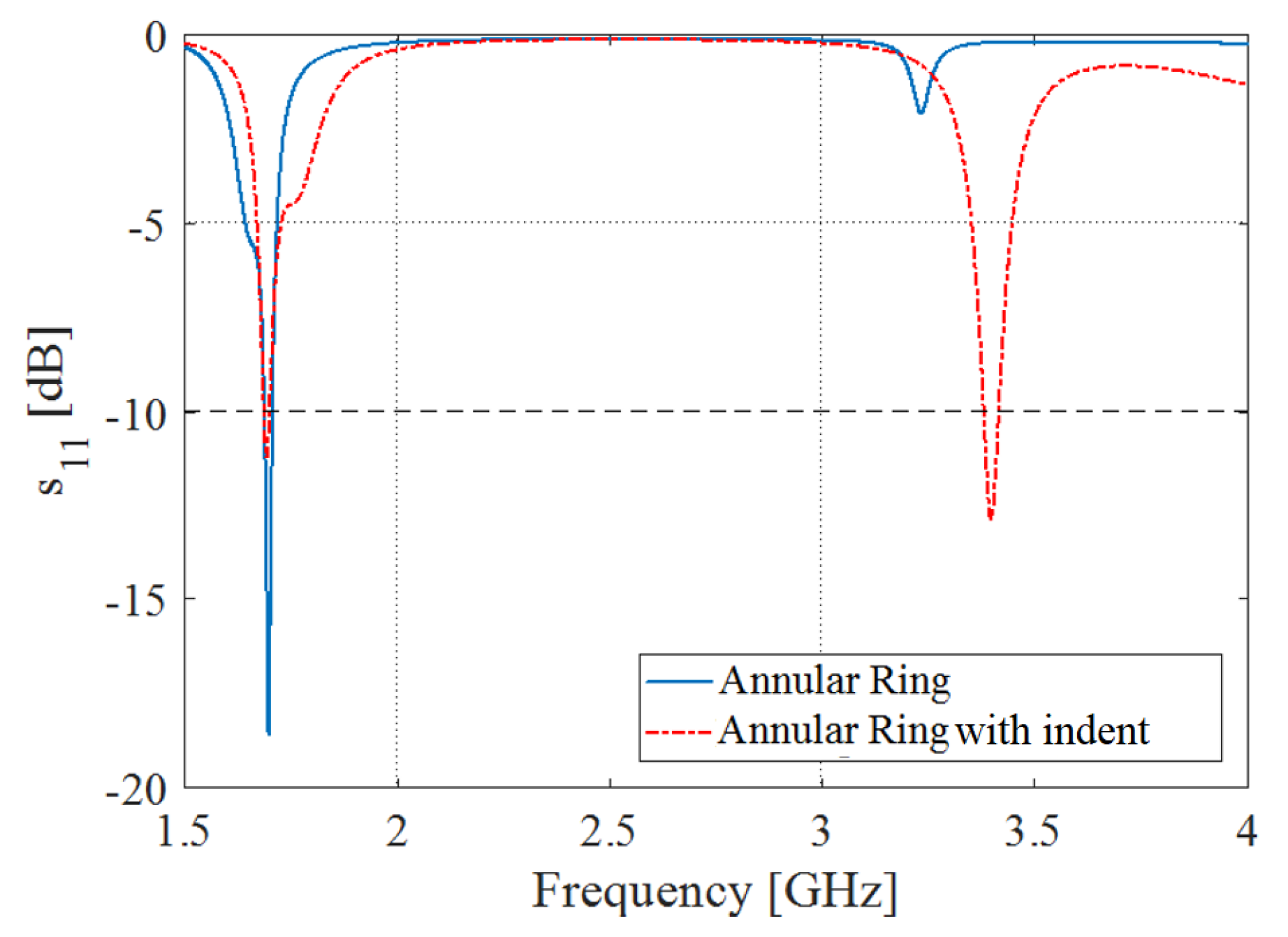
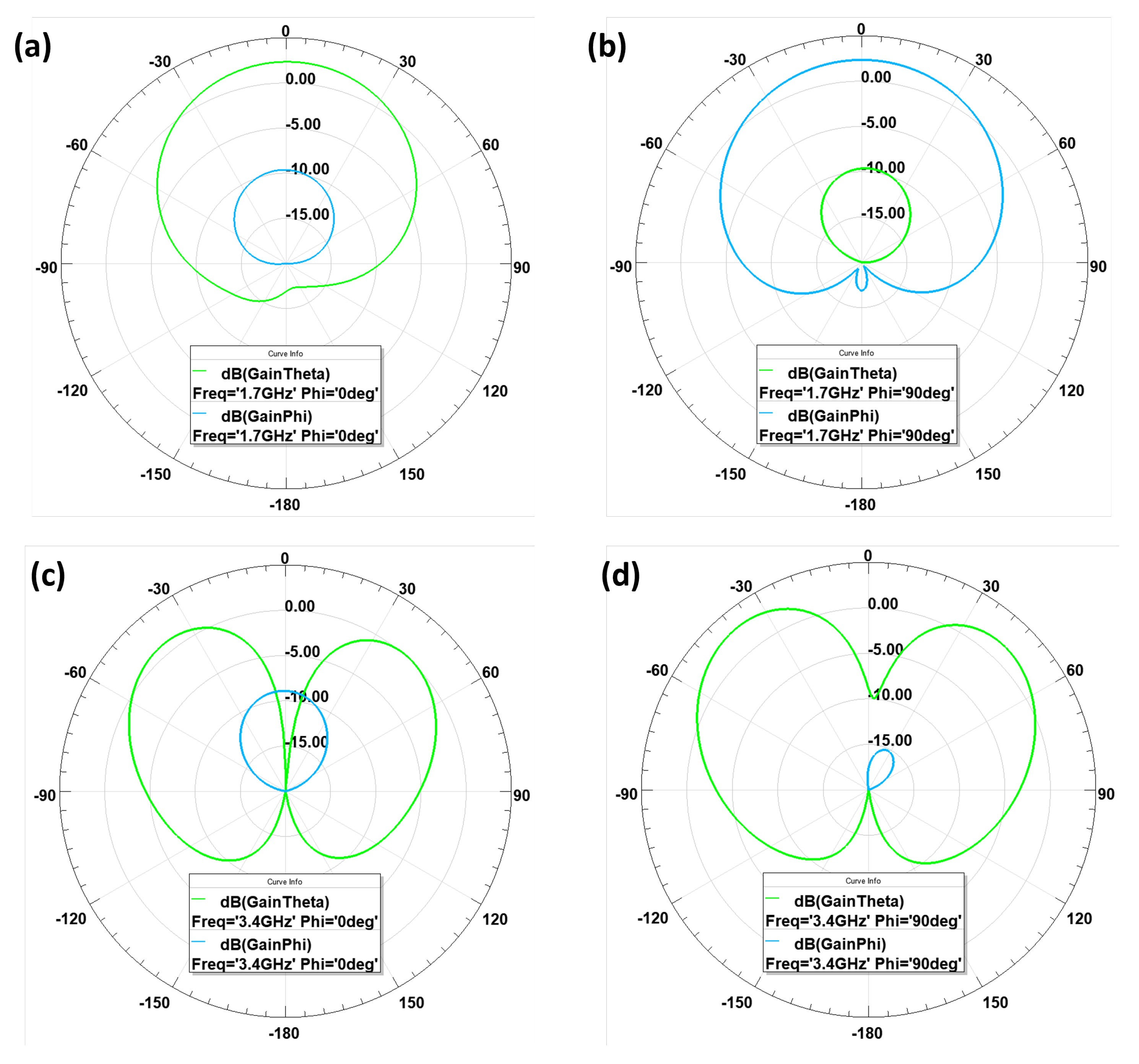
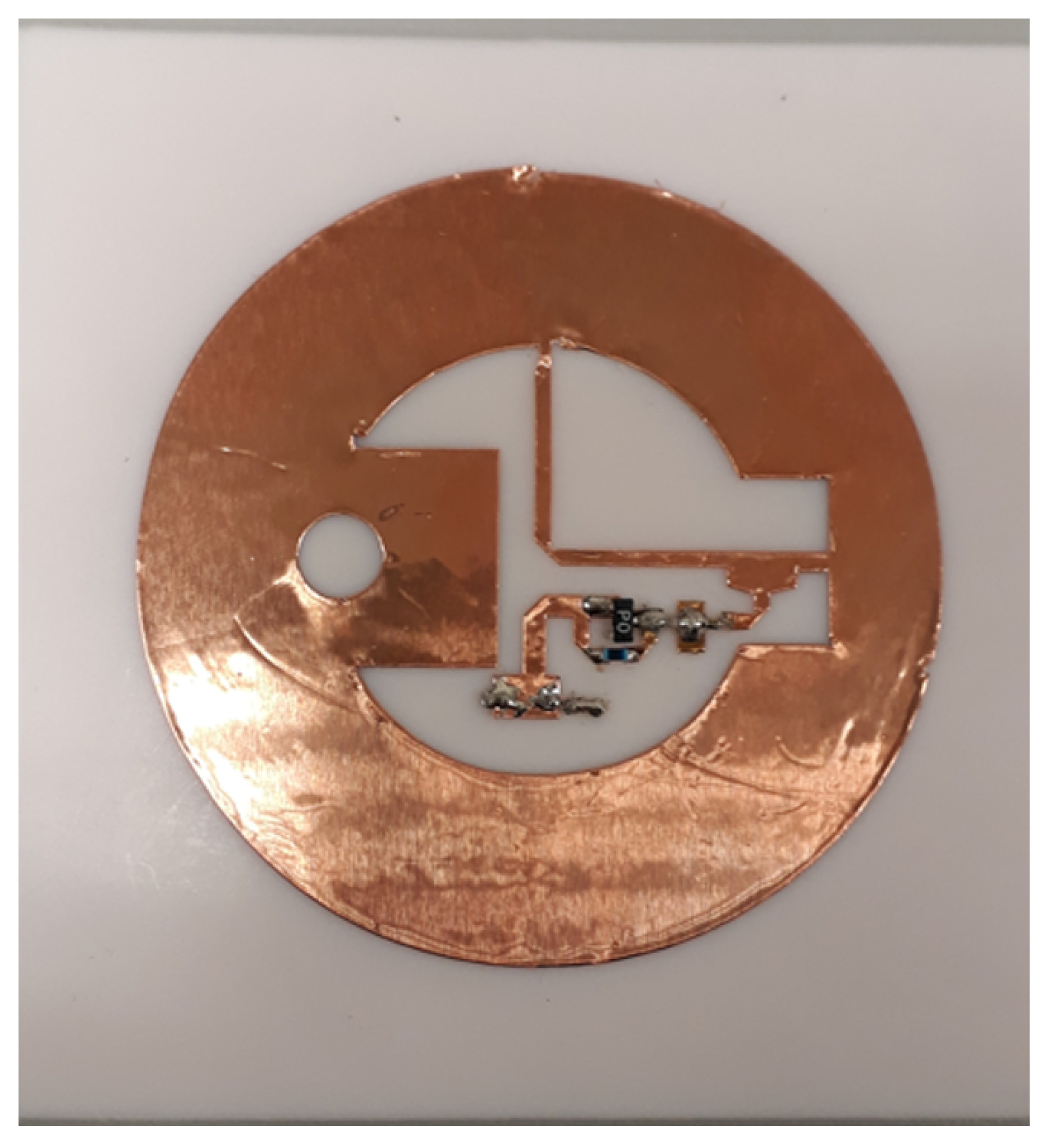
5.2. Measurements of the Realized Antenna

Despite the handmade realization of the antenna prototype, the measurement of the reflection coefficient of the antenna reveals minor discrepancies compared to the simulations, as shown in Figure 15. It is well-matched at both frequencies of 1.7 GHz and 3.4 GHz but simulation results appear a little bit better than measurements.

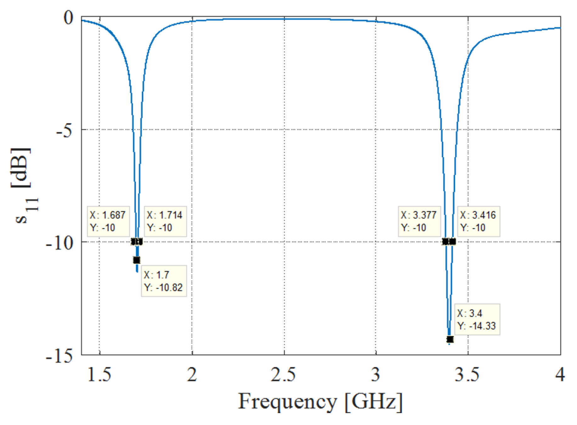
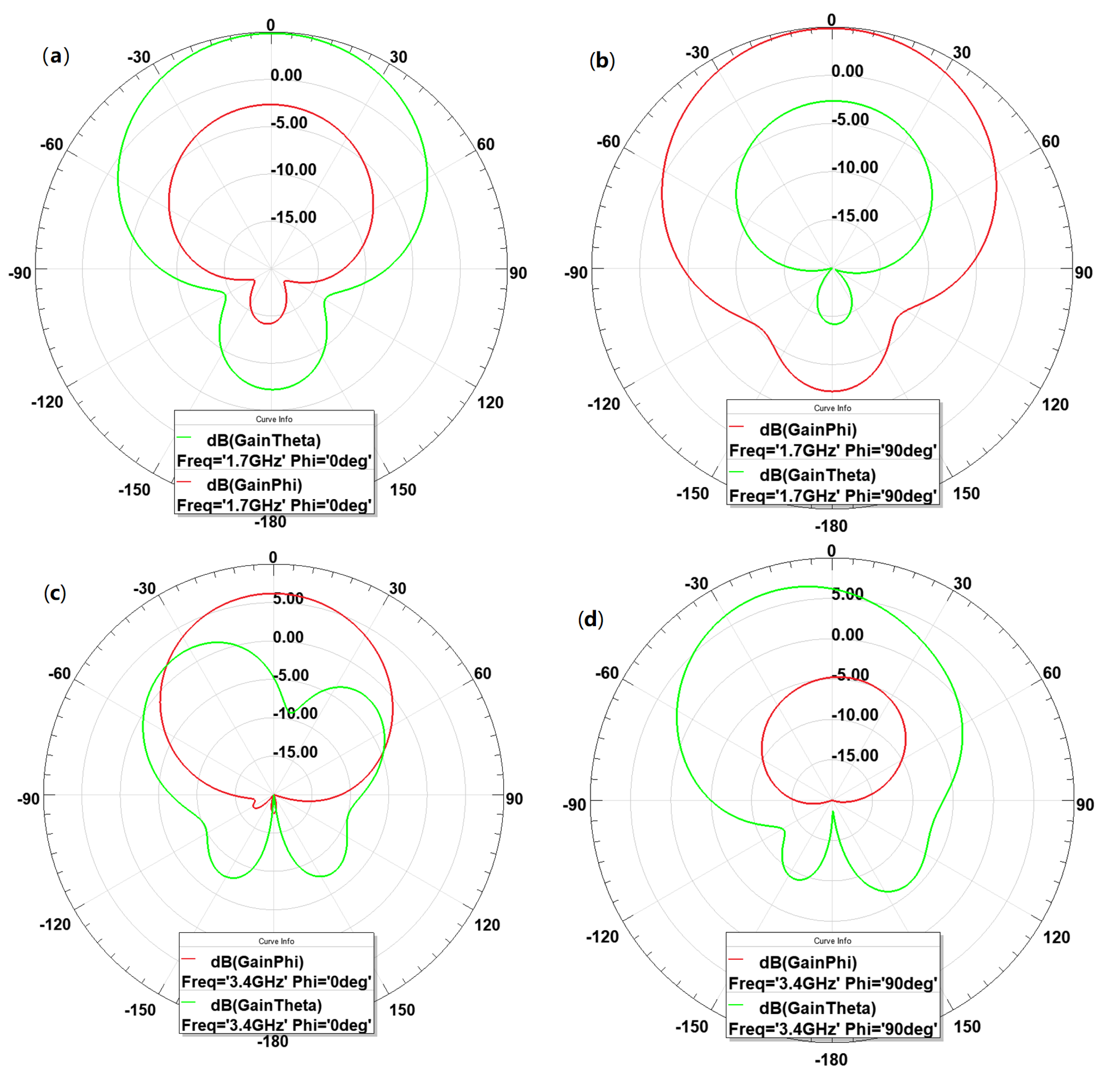
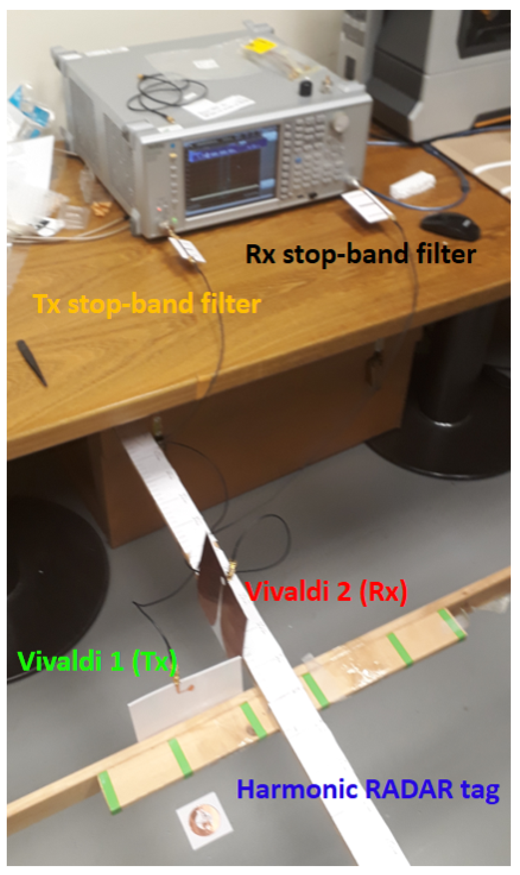
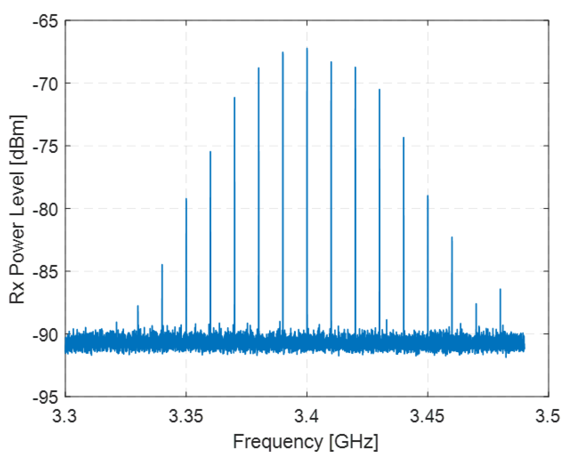
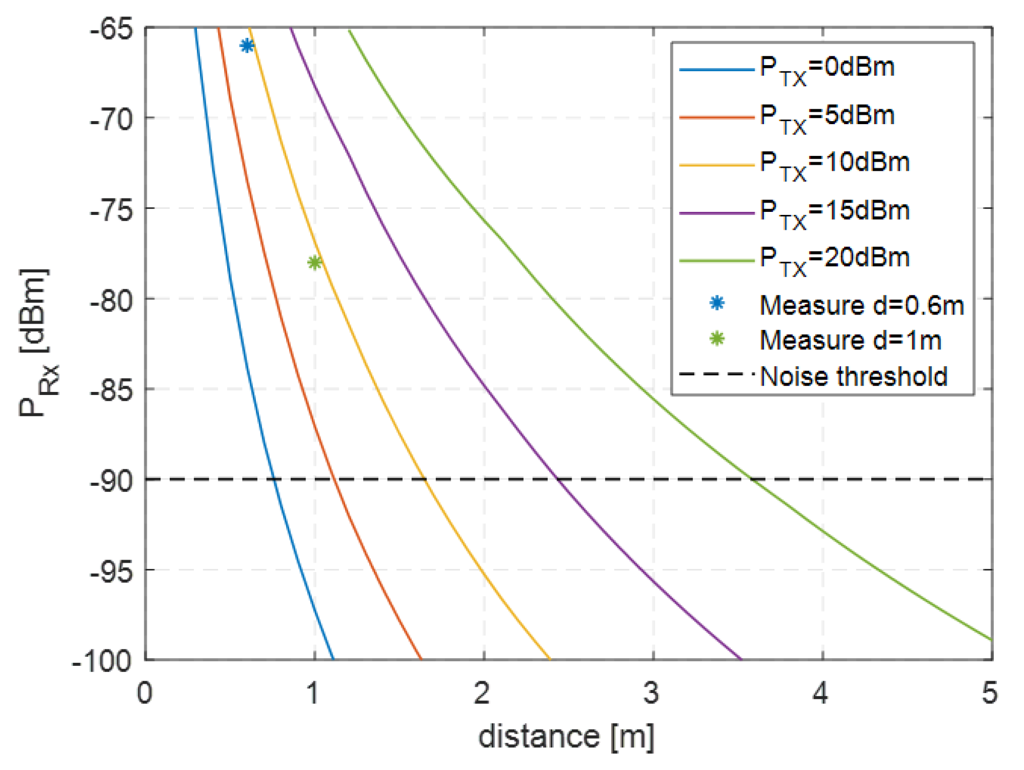
5.3. Measurements of the Complete Tag

The functionality of the complete tag, shown in Figure 18, has been assessed by performing backscattering measurement using the setup shown in Figure 19. It comprises two identical Vivaldi antennas, the Anritsu 2830A, and the two band-reject filters used previously. The Vivaldi antennas are positioned 60 cm away from the tag (deployed on the floor) and are oriented orthogonally to each other to check the cross-polarized behavior of the tag. The Vivaldi antennas exhibit impedance matching with a reflection coefficient below −10 dB over a frequency range from 1.4 GHz to 12 GHz, and a maximum simulated gain of 6 dBi at 1.7 GHz and 6.5 dBi at 3.4 GHz. Continuous wave (CW) signals are transmitted to the tag with a power level of 9 dBm, covering frequencies from 1.62 GHz to 1.72 GHz with a 5 MHz step. The spectral lines in the second harmonic received on the spectrum analyzer are displayed in Figure 20. As evident, a maximum received power level of −67 dBm is achieved at 3.4 GHz, consistent with the reflection coefficients of the matching circuit and the annular ring antenna. In Figure 20, it can be observed that the tag’s response is highest when optimally matched in the first harmonic and degrades as the frequency moves away from this point.
The measured values are consistent with those predicted by the harmonic radar theory described by Equation (2), where symbols P R x 2 f 0 and P T x f 0 stand for power received at second harmonic (i.e., 2 f 0 ) and transmitted at fundamental frequency f 0 , respectively. G R x 2 f 0 and G T x f 0 are gains of receiving (@ 2 f 0 ) and transmitting (@ f 0 ) Vivaldi antennas, λ 0 is the wavelegth at fundamental frequency, R is the distance of the tag, which has gain G T a g 2 f 0 at second harmonic, and C T a g 2 f 0 is the scale factor of the doubler circuit that has been retrieved from measurements shown in Figure 16. Evidently, Equation (2) does not account for the losses in the cables and filters of the measurement setup (Figure 19); therefore, the transmitted and received power is intended at the antenna terminals.
P R x 2 f 0 = 1 4 ( P T x f 0 G T x f 0 G T a g f 0 ) 2 C T a g 2 f 0 G T a g 2 f 0 G R x 2 f 0 λ 0 4 π R 6
Denoting with L the losses of cables and filters used for measurements, the actual received power is P R x = P R x 2 f 0 L . Graphs of P R x are shown in Figure 21 as function of tag distance for different values of the transmitted power. The received power decreases rapidly with the distance from the tag but, for a sufficient transmitted power (for example 20 dBm), the tag can be read from a distance greater than 3 m. The asterisks shown in the picture report the value of the measured received power for a transmitted power of 9 dBm (at the output port of generator) when the tag is at 60 cm and 100 cm of distance. It is evident that the measurements agree well with the theoretical curve.

6. Discussion of Results

A comparison with previous harmonic tags can be conducted from different points of view that evaluate different characteristics of tags. We introduce four different metric keys: type of antenna, number of antennas used in the tag, use of dual polarization, and the conversion losses. The type of antenna is important because the tag must be insensitive to the object on which it is positioned. To satisfy this requirement, groundless antennas can be used only in specific applications where the tag is in the air; in other cases, it is preferable to have a tag with a ground plane. The number of antennas (many harmonic tags use two antennas) can affect the compactness of the tag. The use of dual polarization is preferable to facilitate the distinction of the back-transmitted signal from the clutter. Conversion losses, clearly, allow us to evaluate the quality of the transponder. From the comparison reported in Table 2, it is clear that our tag model has the advantages of having a ground plane, of being sufficiently compact since it is made up of a single antenna, and of using dual polarization. From the point of view of conversion loss it is placed in a median position of the ranking and is in line with the results obtained by other authors. It is interesting to analyze the reasons why the conversion losses of the proposed transponder are 14 dB greater than those of the best in the ranking [23]. Conversion losses can depend on three factors (at least): the type of diode, the material of the substrate on which the transponder is made, and the manufacturing method. From Figure 4 in article [23], we observe that this reference uses the diode SMS7630, which has at least 5 dB lower losses than the HSMS2850. The substrate used in [23] is Rogers RT/duroid 6002 with a dissipation factor of 0.0012, 20 mil thickness, and 18- μ m copper cladding. Our transponder uses a 1.5 mm thick Teflon slab with a dissipation factor of 0.0027 and 35 μ m thick adhesive copper, whose glue adds further losses. Further losses may be due to the manufacturing process, which, in our case, is quite rough, as it was carried out by hand with transmission lines not perfectly stretched over the dielectric slab. Certainly, an improvement in the conversion losses can be obtained by considering a better realization of the transponder using photolithographic techniques and materials with lower losses.

7. Conclusions

This study presents a comprehensive design, prototyping, and measurement analysis of a harmonic tag. By incorporating a dual-band harmonic circuit and a perturbed annular ring patch antenna, able to radiate orthogonal polarization at harmonic frequencies, the tag achieves enhanced performance, adaptability, and flexibility for various wireless sensing applications. The tag has been designed to handle low-power impinging signals and it can be detected at several meters of distance. From the analysis of the obtained results, it is clear that the new concept of single-port transponder is valid and works adequately. The measurements of conversion losses are aligned with those in the literature but there is ample room for improvement; in particular, a more accurate implementation with better technology can improve conversion efficiency. Since the proposed tag is a good candidate to be worn, as a possible future improvement, it can be enriched with sensor functionality.

Author Contributions

Conceptualization, E.D.; Methodology, A.D. (Alessandro DiCarlofelice) and A.D. (Antonio DiNatale); Software, A.D. (Alessandro DiCarlofelice) and A.D. (Antonio DiNatale); Validation, A.D. (Alessandro DiCarlofelice) and A.D. (Antonio DiNatale); Formal analysis, E.D.; Writing—original draft, A.D. (Antonio DiNatale); Writing—review & editing, A.D. (Alessandro DiCarlofelice), E.D. and P.T.; Supervision, E.D. and P.T. All authors have read and agreed to the published version of the manuscript.

Funding

This research received no external funding.

Institutional Review Board Statement

Not applicable.

Informed Consent Statement

Not applicable.

Data Availability Statement

The original contributions presented in this study are included in the article. Further inquiries can be directed to the corresponding author.

Conflicts of Interest

Authors declare that the research was conducted in the absence of any commercial or financial relationships that could be construed as a potential conflict of interest. Author Antonio DiNatale contributed to this research before he was employed by the company Thales Alenia Space Italia.

References

  1. DiNatale, A.; DiCarlofelice, A.; DiGiampaolo, E. A Crack Mouth Opening Displacement Gauge Made with Passive UHF RFID Technology. IEEE Sensors J. 2022, 22, 174–181. [Google Scholar] [CrossRef]
  2. Zhang, D.; Yang, L.T.; Chen, M.; Zhao, S.; Guo, M.; Zhang, Y. Real-Time Locating Systems Using Active RFID for Internet of Things. IEEE Syst. J. 2016, 10, 1226–1235. [Google Scholar] [CrossRef]
  3. Casella, G.; Bigliardi, B.; Bottani, E. The evolution of RFID technology in the logistics field: A review. Procedia Comput. Sci. 2022, 200, 1582–1592. [Google Scholar] [CrossRef]
  4. Potyrailo, R.A.; Nagraj, N.; Tang, Z.; Mondello, F.J.; Surman, C.; Morris, W. Battery-free Radio Frequency Identification (RFID) Sensors for Food Quality and Safety. J. Agric. Food Chem. 2012, 60, 8535–8543. [Google Scholar] [CrossRef]
  5. Hughes, J.D.; Occhiuzzi, C.; Batchelor, J.; Marrocco, G. Twin-Grid Array as 3.6 GHz Epidermal Antenna for Potential Backscattering 5G Communication. IEEE Antennas Wirel. Propag. Lett. 2020, 19, 2092–2096. [Google Scholar] [CrossRef]
  6. Lavric, A.; Popa, V. A LoRaWAN: Long range wide area networks study. In Proceedings of the 2017 International Conference on Electromechanical and Power Systems (SIELMEN), Iasi, Romania, 11–13 October 2017; pp. 417–420. [Google Scholar] [CrossRef]
  7. Nikitin, P.; Rao, K. Performance limitations of passive UHF RFID systems. In Proceedings of the 2006 IEEE Antennas and Propagation Society International Symposium, Albuquerque, NM, USA, 9–14 July 2006; pp. 1011–1014. [Google Scholar] [CrossRef]
  8. Di Carlofelice, A.; Di Giampaolo, E.; Tognolatti, P. A Van-Atta UWB Cross-Polar Chipless Tag to be Used as a Sensor. In Proceedings of the 2023 Photonics & Electromagnetics Research Symposium (PIERS), Prague, Czech Republic, 3–6 July 2023; pp. 698–702. [Google Scholar] [CrossRef]
  9. Athauda, T.; Karmakar, N. Chipped Versus Chipless RF Identification: A Comprehensive Review. IEEE Microw. Mag. 2019, 20, 47–57. [Google Scholar] [CrossRef]
  10. Mondal, S.; Kumar, D.; Chahal, P. Recent Advances and Applications of Passive Harmonic RFID Systems: A Review. Micromachines 2021, 12, 420. [Google Scholar] [CrossRef]
  11. Lach, M.; Hani, M.; Looschen, C.; Buchberger, C.; Biebl, E. Evaluation of UHF-RFID Tag Performance Considering Near-Field and Detuning Effects on Various Dielectric and Inhomogeneous Application Surfaces. In Proceedings of the 2021 Kleinheubach Conference, Miltenberg, Germany, 28–30 September 2021; pp. 1–4. [Google Scholar] [CrossRef]
  12. Mei, L.H.; Yue, W.J.; Kun, X.L.; Xin, Y.T. Influence of UHF tags in the different material surface to RFID system. In Proceedings of the 2014 3rd Asia-Pacific Conference on Antennas and Propagation, Harbin, China, 26–29 July 2014; pp. 713–715. [Google Scholar] [CrossRef]
  13. Zhu, J.; Li, Y.; Jin, C.; Liu, X.; Liu, H. Optimum Separation for Performance Improvement of RFID Solenoid Coil Antenna in Metallic Environments. IEEE Antennas Wirel. Propag. Lett. 2021, 20, 1611–1615. [Google Scholar] [CrossRef]
  14. Faudzi, N.M.; Ali, M.T.; Ismail, I.; Jumaat, H.; Sukaimi, N.H.M. Compact microstrip patch UHF-RFID tag antenna for metal object. In Proceedings of the 2014 IEEE Symposium on Wireless Technology and Applications (ISWTA), Kuala Lumpur, Malaysia, 28 September–1 October 2014; pp. 160–164. [Google Scholar] [CrossRef]
  15. Li, B.; He, Y.; Zuo, L.; Long, Y. Metric of the Application Environment Impact to the Passive UHF RFID System. IEEE Trans. Instrum. Meas. 2014, 63, 2387–2395. [Google Scholar] [CrossRef]
  16. Jouali, R.; Aoutoul, M.; Ouahmane, H.; Ahmad, S.; Had, A.; El Moukhtafi, F.; Parchin, N.O.; See, C.H.; Abd-Alhameed, R. Design of an Analog RFID-Based Tag Antenna with Opened Circuited L-Shaped Stubs for Applications in Localization. Electronics 2022, 11, 1027. [Google Scholar] [CrossRef]
  17. Balog, M.; Szilagyi, E.; Dupláková, D.; Mindas, M. Effect Verification of External Factor to Readability of RFID Transponder Using Least Square Method. Measurement 2016. [Google Scholar] [CrossRef]
  18. Dupláková, D.; Knapčíková, L.; Hatala, M.; Szilagyi, E. Mathematical Modeling of Temperature Characteristics of RFID Tags with their Subsequent Application in Engineering Production. TEM Journa 2016. [Google Scholar] [CrossRef]
  19. Colpitts, B.; Boiteau, G. Harmonic radar transceiver design: Miniature tags for insect tracking. IEEE Trans. Antennas Propag. 2004, 52, 2825–2832. [Google Scholar] [CrossRef]
  20. Recco. Available online: https://recco.com/technology/ (accessed on 7 November 2023).
  21. Palazzi, V.; Alimenti, F.; Kalialakis, C.; Mezzanotte, P.; Georgiadis, A.; Roselli, L. Highly Integrable Paper-Based Harmonic Transponder for Low-Power and Long-Range IoT Applications. IEEE Antennas Wirel. Propag. Lett. 2017, 16, 3196–3199. [Google Scholar] [CrossRef]
  22. Rasilainen, K.; Ilvonen, J.; Lehtovuori, A.; Hannula, J.M.; Viikari, V. On Design and Evaluation of Harmonic Transponders. IEEE Trans. Antennas Propag. 2015, 63, 15–23. [Google Scholar] [CrossRef]
  23. Gu, X.; Srinaga, N.N.; Guo, L.; Hemour, S.; Wu, K. Diplexer-Based Fully Passive Harmonic Transponder for Sub-6-GHz 5G-Compatible IoT Applications. IEEE Trans. Microw. Theory Tech. 2019, 67, 1675–1687. [Google Scholar] [CrossRef]
  24. Pisa, S.; Trifiletti, A.; Tommasino, P.; Monsurrò, P.; Tognolatti, P.; Leuzzi, G.; Di Carlofelice, A.; Di Giampaolo, E. An Intermodulation Radar for Non-Linear Target and Transceiver Detection. Sensors 2024, 24, 1433. [Google Scholar] [CrossRef]
  25. Palazzi, V.; Alimenti, F.; Virili, M.; Mariotti, C.; Orecchini, G.; Mezzanotte, P.; Roselli, L. A novel compact harmonic RFID sensor in paper substrate based on a variable attenuator and nested antennas. In Proceedings of the 2016 IEEE MTT-S International Microwave Symposium (IMS), San Francisco, CA, USA, 22–27 May 2016; pp. 1–4. [Google Scholar] [CrossRef]
  26. Ghazali, M.I.M.; Karuppuswami, S.; Chahal, P. Embedded Passive RF Tags towards Intrinsically Locatable Buried Plastic Materials. In Proceedings of the 2016 IEEE 66th Electronic Components and Technology Conference (ECTC), Las Vegas, NV, USA, 31 May–3 June 2016; pp. 2575–2580. [Google Scholar] [CrossRef]
  27. Mondal, S.; Chahal, P. A Passive Harmonic RFID Tag and Interrogator Development. IEEE J. Radio Freq. Identif. 2019, 3, 98–107. [Google Scholar] [CrossRef]
  28. Yu, F.; Lyon, K.G.; Kan, E.C. A Novel Passive RFID Transponder Using Harmonic Generation of Nonlinear Transmission Lines. IEEE Trans. Microw. Theory Tech. 2010, 58, 4121–4127. [Google Scholar] [CrossRef]
  29. Zhang, L.; Karasiewicz, D.; Cifctioglu, B.; Wu, H. A 1.6-to-3.2/4.8 GHz dual-modulus injection-locked frequency multiplier in 0.18μm digital CMOS. In Proceedings of the 2008 IEEE Radio Frequency Integrated Circuits Symposium, Atlanta, GA, USA, 15–17 June 2008; pp. 427–430. [Google Scholar] [CrossRef]
  30. Wang, C.C.; She, H.C.; Hu, R. A 1.2 GHz programmable DLL-based frequency multiplier for wireless applications. In Proceedings of the 9th International Conference on Electronics, Circuits and Systems, Dubrovnik, Croatia, 15–18 September 2002; Volume 1, pp. 69–72. [Google Scholar] [CrossRef]
  31. ERC Report 025: The European Table of Frequency Allocations and Applications in the Frequency Range 8.3 kHz to 3000 GHz. Available online: https://docdb.cept.org/document/593 (accessed on 4 April 2025).
  32. Murata Manufacturing Co., Ltd. Available online: https://www.murata.com/en-eu (accessed on 7 November 2023).
  33. DiCarlofelice, A.; DiGiampaolo, E.; Tognolatti, P. A Procedure to Design Feasible Dual Band Matching Networks with Minimum Complexity. Electronics 2022, 11, 3569. [Google Scholar] [CrossRef]
  34. AWR Microwave Office Software. Available online: https://www.cadence.com/ko_KR/home/tools/system-analysis/rf-microwave-design/awr-microwave-office.html (accessed on 7 November 2023).
  35. Broadcom Inc. Available online: https://www.broadcom.com/ (accessed on 13 April 2025).
  36. Kubina, B.; Romeu, J.; Mandel, C.; Schüßler, M.; Jakoby, R. Quasi-chipless wireless temperature sensor based on harmonic radar. Electron. Lett. 2014, 50, 86–88. [Google Scholar] [CrossRef]
  37. Ansys HFSS—3D High Frequency Simulation Software. Available online: https://www.ansys.com/products/electronics/ansys-hfss (accessed on 7 November 2023).
  38. Row, J.S. Dual-frequency circularly polarised annular-ring microstrip antenna. Electron. Lett. 2004, 40, 153–154. [Google Scholar] [CrossRef]
  39. James, J.R.; Hall, P.S. Handbook of Microstrip Antennas; Peter Peregrinus Ltd.: London, UK, 1989. [Google Scholar]
Figure 1. Schema of the proposed harmonic tag: a single-port dual-band harmonic circuit (i.e., a doubled-matched doubler) connected to a dual-band antenna.
Applsci 15 04590 g001
Figure 2. Layout of the single-port double-matched doubler circuit for the Schottky HSMS-2850 (Avago Technologies [35]) diode obtained after a two-step optimization (i.e., AWR and HFSS). Dimensions are in millimeters. The table shows the names and the nominal values of the components used. L 1 and C 1 , and L 2 and C 2 are in parallel with each other, respectively.
Applsci 15 04590 g002
Figure 3. Reflection coefficient. These data were obtained from the model developed in Ansys HFSS 2022R1.
Applsci 15 04590 g003
Figure 4. Schema of annular ring microstrip antenna fed by a microstrip line; r o and r i are outer and inner radius, respectively. Red arrows represent currents, crosses position of nulls (or minima) of current, circles maxima of current. On right side, the corresponding radiation patterns. (a) T M 11 mode; (b) T M 21 mode.
Applsci 15 04590 g004
Figure 5. Schema of a modified annular ring microstrip antenna fed by a microstrip line and connected to an open-circuit stub. Red arrows represent currents, crosses position of nulls (minima) of currents, circles maxima of current. Currents of T M 21 mode are affected by currents over the stub (protrusion). On the right side is shown the corresponding radiation pattern.
Applsci 15 04590 g005
Figure 6. (a) Initial layout of the annular ring antenna with relevant symbolic dimensions; (b) Application of the rectangular indent near the feed point located on the horizontal microstrip line.
Applsci 15 04590 g006
Figure 7. Reflection coefficient obtained in simulation for the layouts shown in Figure 6.
Applsci 15 04590 g007
Figure 8. Radiation pattern of the gain expressed in dBi: (a) results obtained at 1.7 GHz for ϕ = 0 ; (b) results obtained at 1.7 GHz for ϕ = 90 ; (c) results obtained at 3.4 GHz for ϕ = 0 ; (d) results obtained at 3.4 GHz for ϕ = 90 . In the figures, the green curves represent the θ component, and the light blue ones are the ϕ component.
Applsci 15 04590 g008
Figure 9. Layout of the annular ring antenna provided with the holed protrusion (stub) placed in the opposite direction from the rectangular indent.
Applsci 15 04590 g009
Figure 10. Reflection coefficient of the antenna after adding the rectangular protrusion inside the inner perimeter of the ring composing the antenna.
Applsci 15 04590 g010
Figure 11. Radiation patterns of the gain expressed in dBi: (a) results obtained at 1.7 GHz for ϕ = 0 ; (b) results obtained at 1.7 GHz for ϕ = 90 ; (c) results obtained at 3.4 GHz for ϕ = 0 ; (d) results obtained at 3.4 GHz for ϕ = 90 . In the figures, the green curves represent the gain plot of θ component, and the red ones are the ϕ component.
Applsci 15 04590 g011
Figure 12. Surface currents flowing on the surface of the annular patch: (a) currents at 1.7 GHz; (b) currents at 3.4 GHz.
Applsci 15 04590 g012
Figure 13. RCS for vertical polarization (dotted lines): comparison between the antenna alone (violet dotted line) and the complete tag (i.e., antenna including the doubler circuit) (black dotted line). The deep notch at 1.7 GHz corresponds to the resonance of the antenna operating with T M 11 mode; the small notch at 3.4 GHz mainly depends on the matching condition between the antenna and the doubler circuit at that frequency. RCS for horizontal polarization (solid lines): comparison between the antenna alone (blue line) and the complete tag (i.e., antenna including the doubler circuit) (red line). The deep notch at 3.4 GHz corresponds to the resonance of T M 21 mode, while the small notch at 1.7 GHz depends on the matching conditions between the antenna and the doubler circuit.
Applsci 15 04590 g013
Figure 14. Fabricated prototypes: (a) matching circuit for Schottky zero-bias diode HSMS-2850; (b) annular patch antenna (final layout).
Applsci 15 04590 g014
Figure 15. Reflection coefficient for both circuit and antenna: comparison between measurements and simulations.
Applsci 15 04590 g015
Figure 16. Measurement of conversion loss of doubler circuit. (a) Measurement setup: transmitted CW signal at 1.7 GHz with different power levels, received power at 3.4 GHz; (b) Received power at 3.4 GHz vs. transmitted power at 1.7 GHz (insertion loss removed).
Applsci 15 04590 g016
Figure 17. Reflection and transmission coefficients of band-reject filters used in the measurement setup.
Applsci 15 04590 g017
Figure 18. Prototype of the final harmonic tag.
Applsci 15 04590 g018
Figure 19. Measurement scenario of the harmonic tag: the tag rests on the floor while two Vivaldi antennas arranged orthogonally and suspended by means of wooden slats are used to transmit and receive.
Applsci 15 04590 g019
Figure 20. Spectrum measured in second harmonic when the distance between the tag and Vivaldi antennas is about 0.6 m.
Applsci 15 04590 g020
Figure 21. Received power vs. tag distance for different values of the transmitted power. Curves: theoretical prediction of harmonic radar equation, including the insertion loss of the measurement sutup; asterisks: measurement results for transmitted power of 9 dBm.
Applsci 15 04590 g021
Table 1. Final antenna dimensions.
Parameters[mm]
r i 14.52
r o 27.07
lfeed1
wfeed4.71
w1.14
yport14.9
lh4.91
wh11.1
lstub12.12
wstub15
rcirc-slot2.81
ycirc-slot4.62
Table 2. Comparison with the literature.
Ref.Antenna TypeN.Dual Pol.Conv. Loss (dB)
[22]meander dipole1No19.9 @-25 dBm
[28]dipole-like2No30 @-20 dBm
[25]annular slot2Yes30 @-25 dBm
[26]slot dipole1No60 @ 0 dBm
[23]spiral slot1No16 @-25 dBm
This workmicrostrip annual ring1Yes30 @-25 dBm
Disclaimer/Publisher’s Note: The statements, opinions and data contained in all publications are solely those of the individual author(s) and contributor(s) and not of MDPI and/or the editor(s). MDPI and/or the editor(s) disclaim responsibility for any injury to people or property resulting from any ideas, methods, instructions or products referred to in the content.

