Article

A CFOA-Based Voltage-Mode Multifunction Biquadratic Filter and a Quadrature Oscillator Using the CFOA-Based Biquadratic Filter

1
Department of Electronic Engineering, National Chin-Yi University of Technology, Taiping, Taichung 41170, Taiwan
2
Department of Electronic Engineering, Ming Chi University of Technology, New Taipei 24301, Taiwan
3
Department of Electrical Engineering, California State University Fullerton, Fullerton, California, CA 92831, USA
*
Author to whom correspondence should be addressed.
Appl. Sci. 2019, 9(11), 2304; https://doi.org/10.3390/app9112304
Submission received: 29 April 2019 / Revised: 31 May 2019 / Accepted: 31 May 2019 / Published: 4 June 2019
(This article belongs to the Section Electrical, Electronics and Communications Engineering)

Abstract

:
This paper proposes a new high-input impedance current feedback operational amplifier (CFOA)- based voltage-mode multifunction biquadratic filter and a voltage-mode quadrature oscillator using the proposed high-input impedance CFOA-based biquadratic filter. The proposed high-input impedance CFOA-based voltage-mode multifunction biquadratic filter uses three CFOAs, three resistors, and two grounded capacitors with two inputs and three outputs. The filter can simultaneously realize non-inverting low-pass, non-inverting band-pass, and non-inverting band-reject filtering functions at the high-input impedance terminal while the inverting band-pass and non-inverting high-pass filtering functions can also be obtained by applying another high-input impedance terminal. The filter offers orthogonal control of resonance angular frequency and quality factor. The proposed high-input impedance CFOA-based voltage-mode multifunction biquadratic filter can be used to implement a voltage-mode quadrature oscillator with an independently controlled the frequency of oscillator and the condition of oscillation. The OrCAD PSpice simulation and experimental results of the commercially available integrated circuit, AD844AN, are used to confirm the characteristics of the proposed filter and oscillator.

1. Introduction

Active filters and oscillators have received significant attention in analog systems because they are frequently used in electrical and electronic engineering works [1,2,3,4,5,6,7]. The current feedback operational amplifiers (CFOAs) are very attractive elements used for realizing active filters and oscillators. CFOAs have an extended bandwidths and higher slew rates advantage over conventional voltage operational amplifiers [8,9,10]. The CFOA has terminal characteristics like positive second generation current-conveyor (CCII+) followed by a voltage buffer (VB) [11,12]. The most commercial CFOA, such as the AD844AN from Analog Devices, has obtained the acceptance of researchers as an active building block in analog circuit design [13,14]. The CFOA differs from the traditional operational amplifier in that the voltage on the non-inverting input terminal is transferred to the inverting input terminal and the inverting input terminal is of low input impedance.
Many voltage-mode CFOA-based universal biquadratic filters have been proposed in the literature [14,15,16,17,18,19,20]. These circuit configurations can realize all the standard transfer functions by selecting different input voltages. However, they require the injection of an excitation signal from one terminal of the capacitor in each circuit design and only one/two standard filtering functions at most can be simultaneously obtained in each circuit realization. A multiple inputs and single output universal filter using four CFOAs, five resistors, and two grounded capacitors has been reported in the literature [21]. This circuit provides the features of orthogonal control of resonance angular frequency (ωo) and quality factor (Q), using only grounded capacitors as well as high-input impedance. However, this reported circuit needs to employ four CFOAs and needs a component matching condition for realizing the all-pass filtering function. The configuration in the literature [22] proposed another three-input single-output CFOA-based biquadratic filter. This configuration employs three CFOAs, five resistors, and two grounded capacitors. The circuit also provides the features of orthogonal control of ωo and Q, using only grounded capacitors as well as high-input impedance. However, this circuit still needs a component matching condition for realizing the all-pass filtering function. It is known that a useful feature of the multifunction biquadratic filter is that the low-pass, band-pass, high-pass, and/or band-reject outputs are simultaneously available at various nodes in the circuit. These additional outputs can be used in some systems that employ more than one filter function [23]. Hence, four CFOA-based universal biquadratic filters were proposed in the literature [24]. These proposed configurations can simultaneously realize low-pass, band-pass, and high-pass responses and have several other possible applications such as in crossover networks used in three-way high-fidelity loudspeakers, and phase-locked loop frequency modulation stereo demodulators [25]. Of particular interest here are the voltage-mode CFOA-based multifunction biquadratic filters [26,27,28,29]. Therefore, a voltage-mode non-inverting low-pass (LP), inverting band-pass (IBP), and non-inverting band-reject (BR) filter employing three CFOAs, three resistors, and two grounded capacitors has been proposed in the literature [26] but it does not offer high-input impedance. Another voltage-mode LP, non-inverting band-pass (BP), and non-inverting high-pass (HP) filter employing three CFOAs, four resistors, and three grounded capacitors has been proposed in the literature [27] but it suffers from the drawback of using three capacitors. A high-input impedance voltage-mode LP, IBP, HP, and BR filter employing four CFOAs, four resistors, and two grounded capacitors has been proposed in the literature [28] but it suffers from the drawback of using four CFOAs. A high-input impedance voltage-mode LP, BP, and HP filter employing three CFOAs, four resistors, and two grounded capacitors has been proposed in the literature [29] but it has a capacitor connected in series to the X port of the CFOA. Because the CFOA has a non-negligible output parasitic resistance on port X, RX, when the X port of CFOA is loaded by a capacitor, it leads to an improper transfer of functions.
In this paper, a new high-input impedance multifunction biquadratic filter configuration with two inputs and three outputs using three CFOAs, three resistors, and two grounded capacitors has been presented. The circuit realizes LP, BP, and BR voltage responses, simultaneously, by the use of only a single voltage input signal while the IBP and HP responses can be obtained by the use of another high-input impedance of input voltage signal. The circuit exhibits high-input impedance and orthogonal control of ωo and Q. Moreover, the proposed CFOA-based voltage-mode multifunction biquadratic filter can be easily converted to a voltage-mode quadrature oscillator. Contrary to the previously reported CFOA-based voltage-mode multifunction biquadratic filters [26,27,28,29], the proposed filter meets all of the following advantages—(i) employs only three CFOAs, three resistors, and two grounded capacitors, (ii) can have simultaneously LP, BP, and BR filtering responses with a single input and three outputs by the use of only a single voltage input signal while the IBP and HP filtering responses can be realized by the use of another input voltage signal, (iii) has high-input impedance, (iv) has orthogonal control of ωo and Q, (v) has no capacitors bringing extra poles that degrade its high frequency performance, (vi) requires no inverting-type voltage input signals, and (vii) can transfer into a voltage-mode quadrature sinusoidal oscillator easily. The properties of the proposed filter and oscillator have been verified by PSpice simulations and furthermore by experimental measurements. The proposed circuit is compared with previously published voltage-mode multifunction biquadratic filters using CFOAs in Table 1.

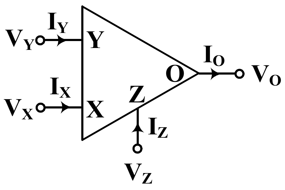
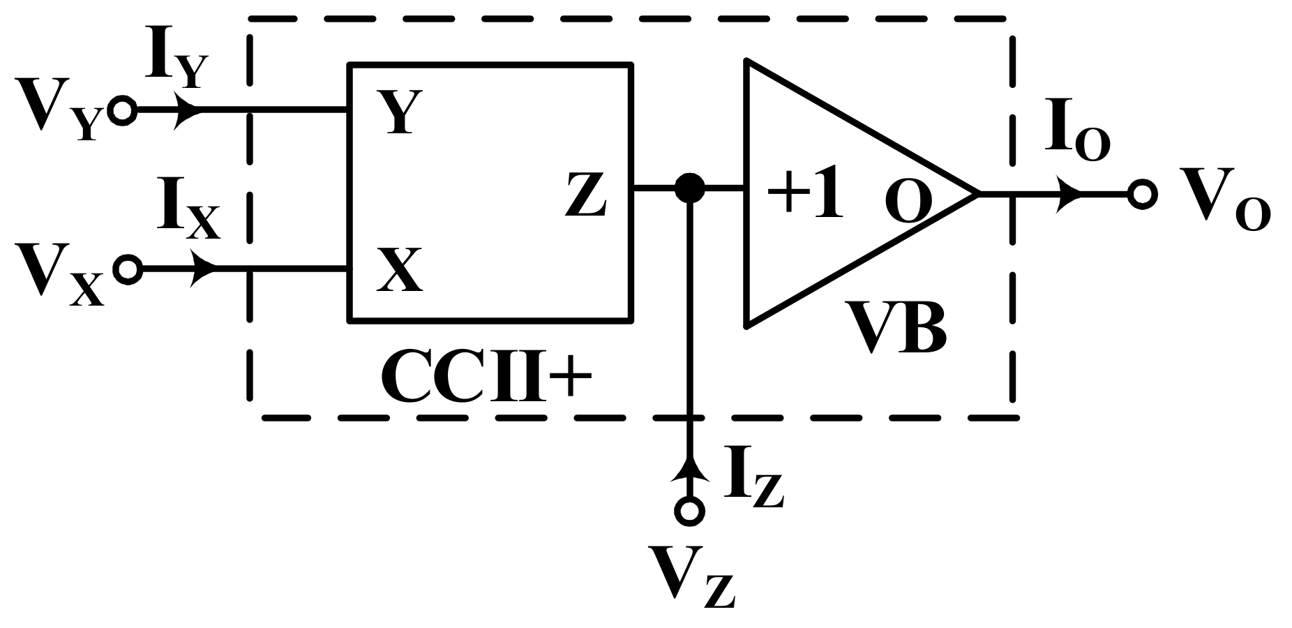
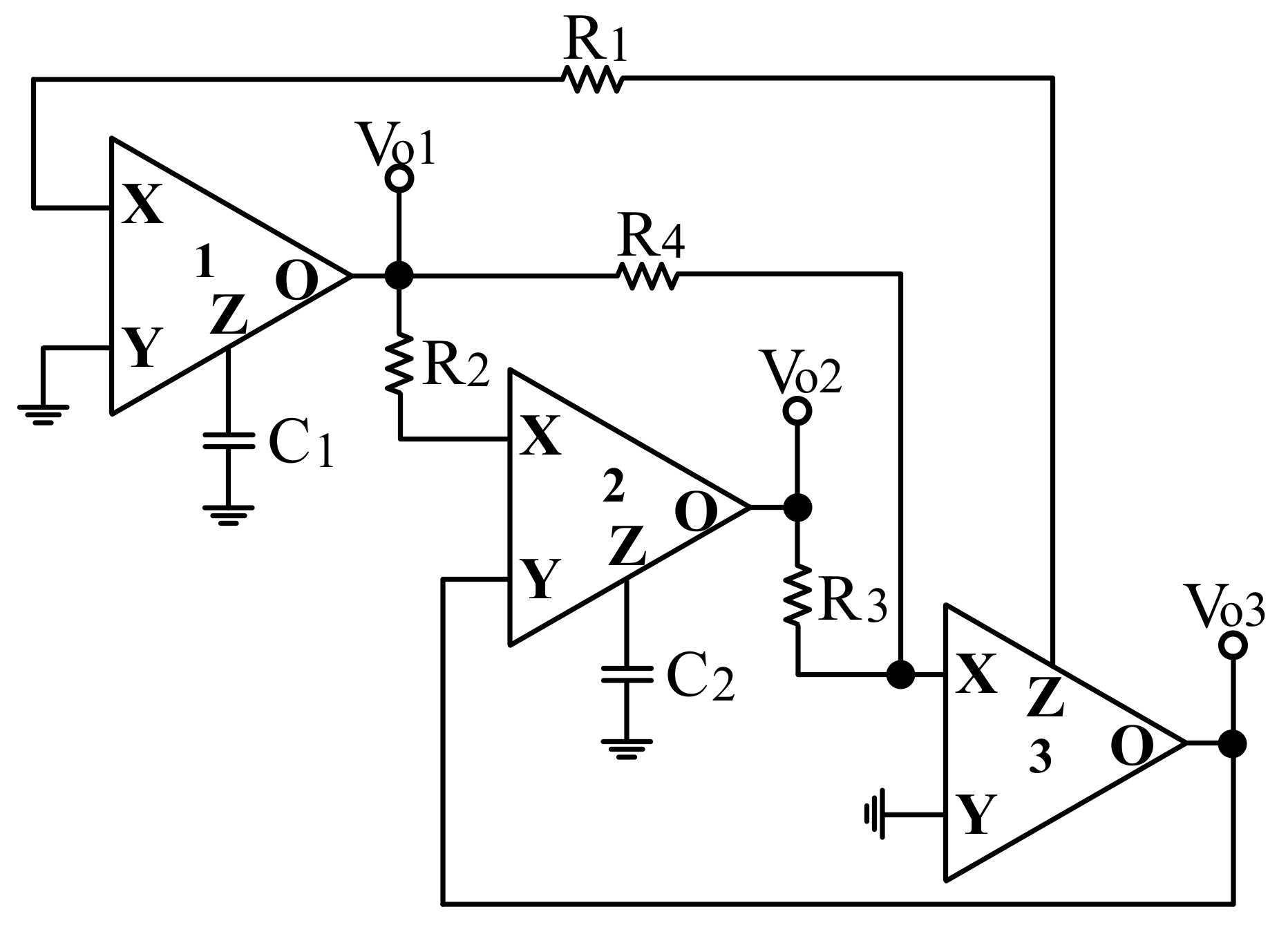
2. Proposed Circuits

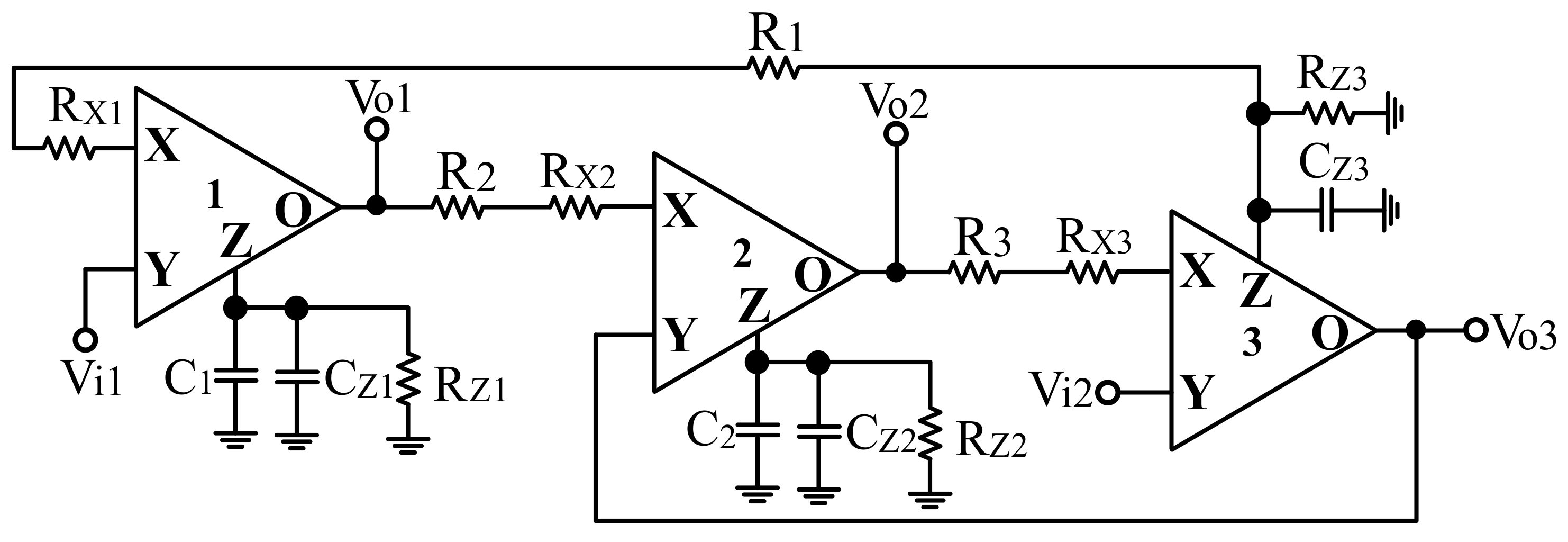
2.1. Voltage-Mode Multifunction Biquadratic Filter

The CFOA is a four-terminal analog building block shown symbolically in Figure 1 [11], with a describing matrix equation of the following form:
[ I Y V X I Z V O ] = [ 0 0 0 0 1 0 0 0 0 1 0 0 0 0 1 0 ] [ V Y I X V Z I O ]
The CFOA is realized by the cascaded connection of a CCII+ followed by a VB, as shown in Figure 2 [11,12]. It gathers the advantages of the CCII+ and VB such as—high input impedance (Y terminal), low input impedance (X terminal), low output impedance (O terminal), high output impedance (Z terminal), high accuracy, and large bandwidth. The voltage at terminal X follows the voltage at terminal Y in magnitude. The output current at terminal Z follows the current at terminal X in magnitude. The voltage drop at terminal Z will be send to terminal O with the unity voltage gain. The proposed high-input impedance voltage-mode CFOA-based biquadratic filter with two inputs and three outputs is shown in Figure 3, which consists of three CFOAs, two grounded capacitors, and three resistors. The use of the grounded capacitors is particularly attractive for integrated circuit (IC) implementation. In Figure 3, the input voltage signal is connected directly to the Y-terminal of the CFOA and the input current to the Y-terminal of the CFOA is zero, the circuit has the feature of high-input impedance. Routine analysis of the filter in Figure 3 gives the following three output voltages:
V o 1 = V i 1 s C 2 R 2 V i 2 s 2 C 1 C 2 R 2 R 3 + s C 1 R 1 + 1
V o 2 = s C 1 R 3 V i 1 + ( s C 1 R 1 + 1 ) V i 2 s 2 C 1 C 2 R 2 R 3 + s C 1 R 1 + 1
V o 3 = ( s 2 C 1 C 2 R 2 R 3 + 1 ) V i 1 + s 2 C 1 C 2 R 1 R 2 V i 2 s 2 C 1 C 2 R 2 R 3 + s C 1 R 1 + 1
As indicated by Equations (2)–(4), if Vi2 = 0 (grounded) and Vi1 = Vin is given by the input voltage signal then the LP, BP, and BR filtering functions are given by:
V o 1 V i n = V L P V i n = 1 s 2 C 1 C 2 R 2 R 3 + s C 1 R 1 + 1
V o 2 V i n = V B P V i n = s C 1 R 3 s 2 C 1 C 2 R 2 R 3 + s C 1 R 1 + 1
V o 3 V i n = V B R V i n = s 2 C 1 C 2 R 2 R 3 + 1 s 2 C 1 C 2 R 2 R 3 + s C 1 R 1 + 1
By letting Vi1 = 0 (grounded) and proving Vi2 = Vin, the IBP and HP filtering functions can be easily obtained from the two voltage outputs Vo1 and Vo3 as follows:
V o 1 V i n = V I B P V i n = s C 2 R 2 s 2 C 1 C 2 R 2 R 3 + s C 1 R 1 + 1
V o 3 V i n = V H P V i n = s 2 C 1 C 2 R 1 R 2 s 2 C 1 C 2 R 2 R 3 + s C 1 R 1 + 1
As illustrated in Equations (5)–(9), the proposed filter simultaneously provides LP, BP, and BR voltage responses while the IBP and HP responses can also be obtained. The pass-band gains, GBP, GIBP, and GHP, for the BP, IBP, and HP responses are given by:
G BP = R 3 R 1 ,   G IBP = C 2 R 2 C 1 R 1 ,   G HP = R 1 R 3
Table 2 summarizes the two inputs and three outputs CFOA-based voltage-mode multifunction biquadratic filter of the transfer functions.
Comparing the expression for the denominator to the characteristic equation D ( s ) = s 2 + ω 0 Q s + ω 0 2 , the parameters ωo and Q of the proposed filter are given by:
ω o = 1 C 1 C 2 R 2 R 3
Q = 1 R 1 C 2 R 2 R 3 C 1
Equations (11) and (12) show that the parameter Q can be tuned by adjusting the resistor R1 without affecting ωo. In other words, Q and ωo are orthogonally adjustable. The orthogonal controllability is a desirable property for the designing and tuning flexibility of the biquadratic filters.

2.2. Voltage-Mode Quadrature Sinusoidal Oscillator

In Figure 3, by inserting a resistance between the voltage output Vo1 and terminal X of the third CFOA, the presented CFOA-based voltage-mode multifunction biquadratic filter can be converted into a voltage-mode quadrature oscillator by making Vi1 = Vi2 = 0. As shown in Figure 4, a new voltage-mode quadrature sinusoidal oscillator based on the proposed filter in Figure 3 is proposed.
The characteristic equation of the quadrature oscillator in Figure 4 can be expressed as:
s 2 C 1 C 2 R 2 R 3 + s ( C 1 R 1 C 2 R 2 R 3 R 4 ) + 1 = 0
The frequency of oscillator (FO) and the condition of oscillation (CO) of Figure 4 can be obtained as:
FO :   ω o = 1 C 1 C 2 R 2 R 3
CO :   C 1 R 1 R 4 C 2 R 2 R 3
For R1 = R2 = R, and C1 = C2 = C, Equations (14) and (15) simplifies to:
FO :   ω o = 1 C 1 R R 3
CO :   R 4 R 3
From Equations (16) and (17), the FO can be controlled by adjusting the value of resistor R without affecting the CO. The CO can be controlled by adjusting the value of resistor R4 without affecting the FO. This means that the FO and CO can be controlled independently by different two resistors. The two marked voltages, Vo1 and Vo3, in the circuit of Figure 4 are related as:
V o 1 V o 3 = 1 s C 1 R 1
Under sinusoidal steady state, Equation (18) can be expressed as:
V o 1 V o 3 = 1 ω o C 1 R 1 e j φ
where the phase difference is of φ = 90 , ensuring the voltages, Vo1 and Vo3, are in quadrature.

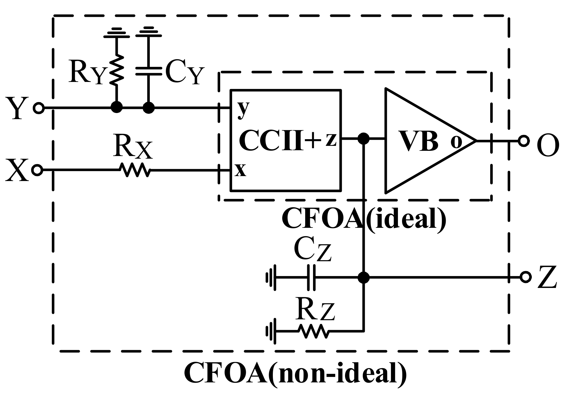
3. Non-Idealities Analysis

Taking the non-idealities of the CFOA into account, Figure 5 shows the non-ideal behavior of a CFOA that has the parasitic input resistance, RX, at the X-terminal. The parasitic resistances, RY and RZ, and parasitic capacitances, CY and CZ, appear between the high-impedance Y and Z terminals and ground, respectively [22]. In the presence of these parasitic elements, the proposed CFOA-based biquadratic filter as shown in Figure 3 can be modified to Figure 6. In Figure 6, the influence of the parasitic resistance, RX, and capacitance, CZ, can be reduced, by selecting the external resistor and capacitor to be much greater than the parasitic resistance and capacitance, respectively. Hence, the effect of parasitic resistance can be easily absorbed as a part of the main resistance and the effect of parasitic capacitance can be easily absorbed as a part of the main capacitance. To reduce the parasitic impedance effects of CFOAs at the Z terminals, the following conditions must be satisfied:
1 s ( C 1 + C Z 1 ) < < R Z 1
1 s ( C 2 + C Z 2 ) < < R Z 2
R 1 + R X 1 < < R Z 3 1 + s R Z 3 C Z 3 .

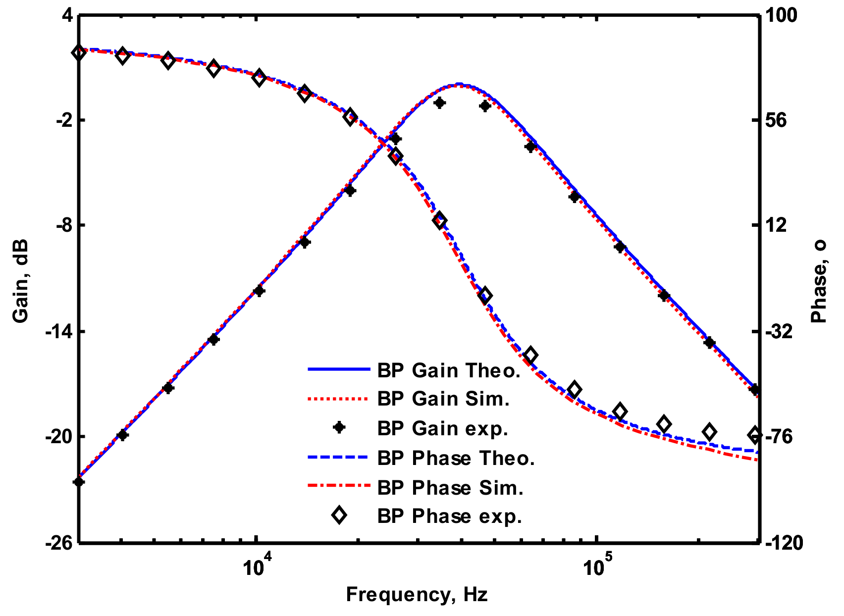
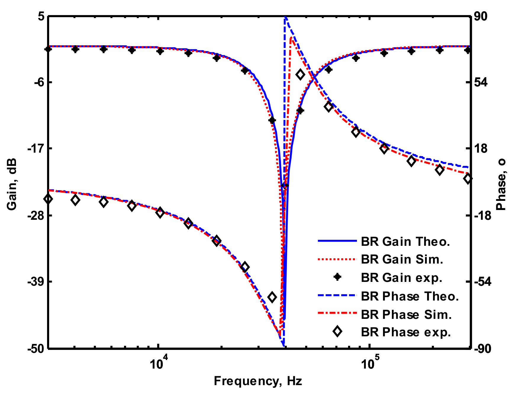
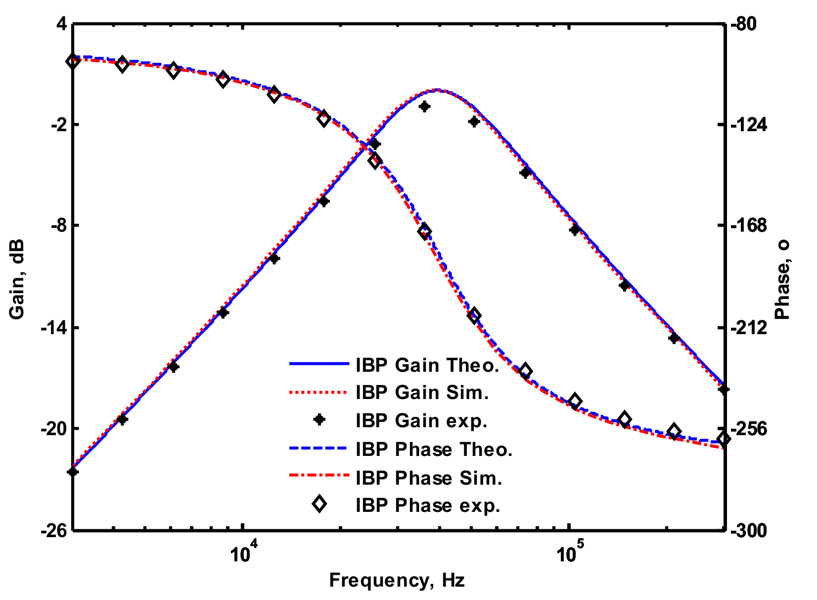
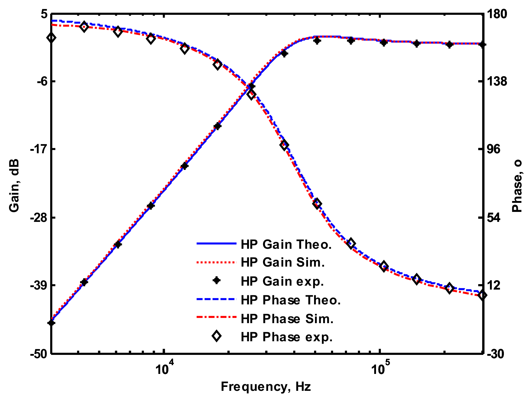
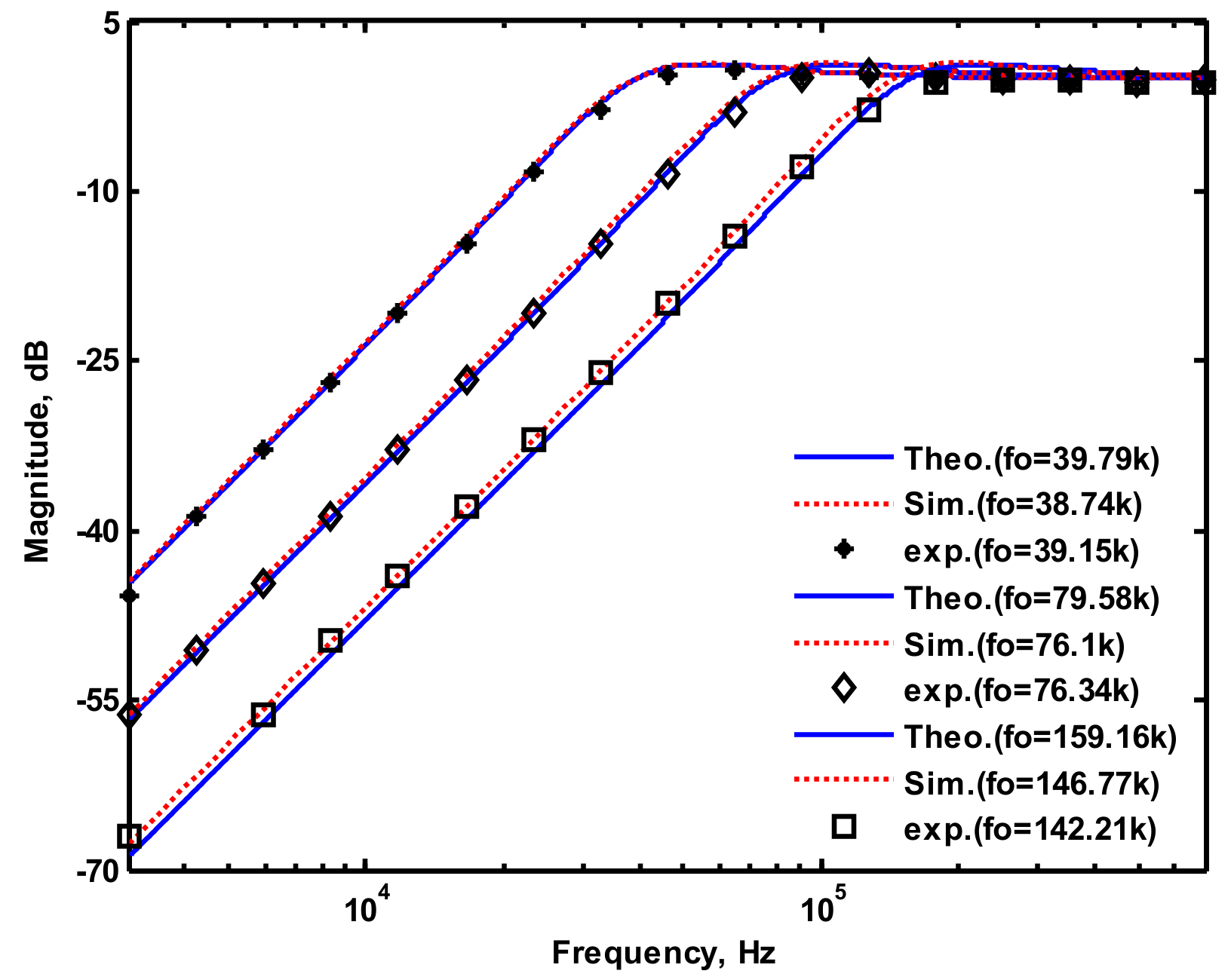
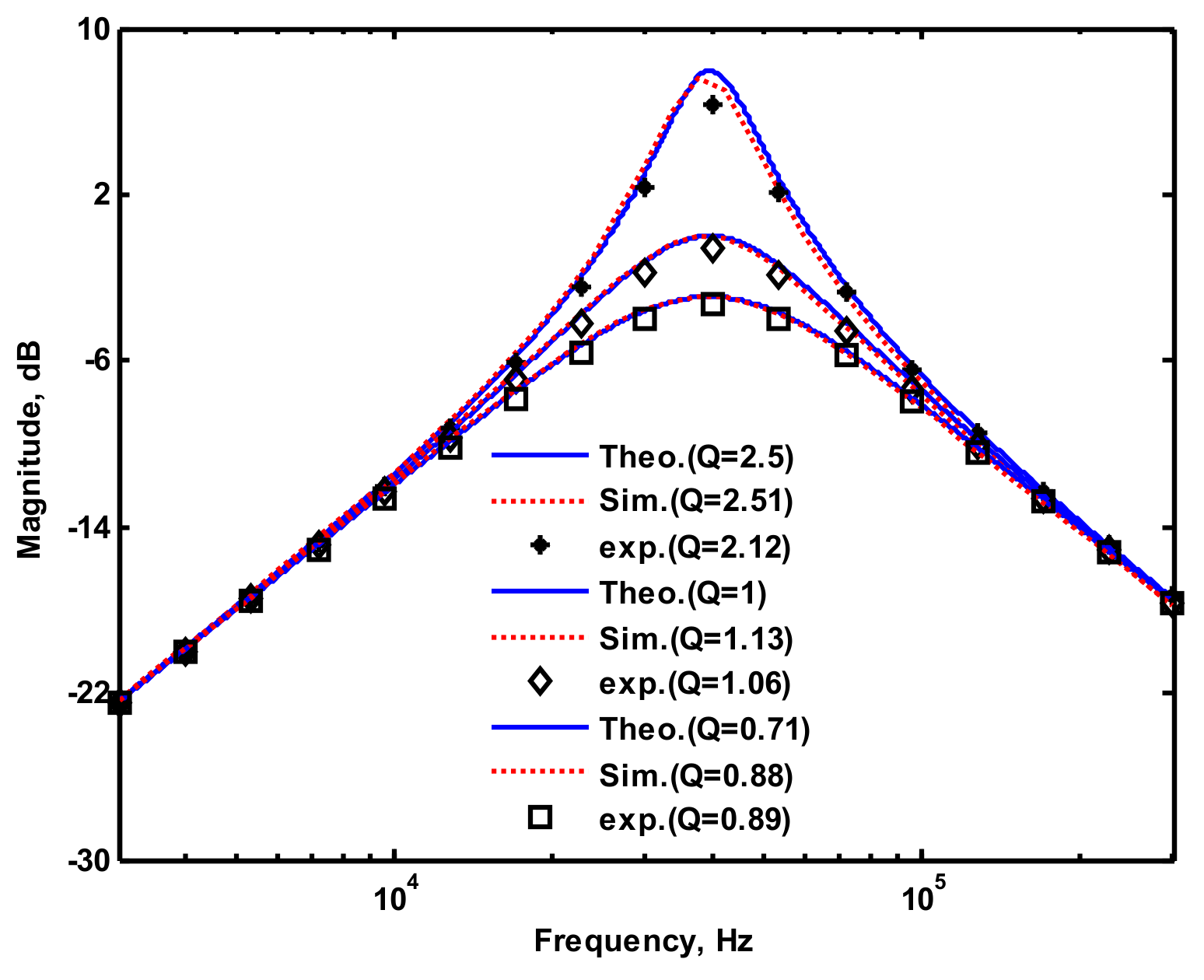
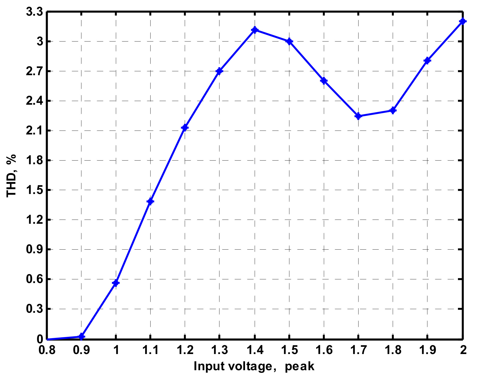
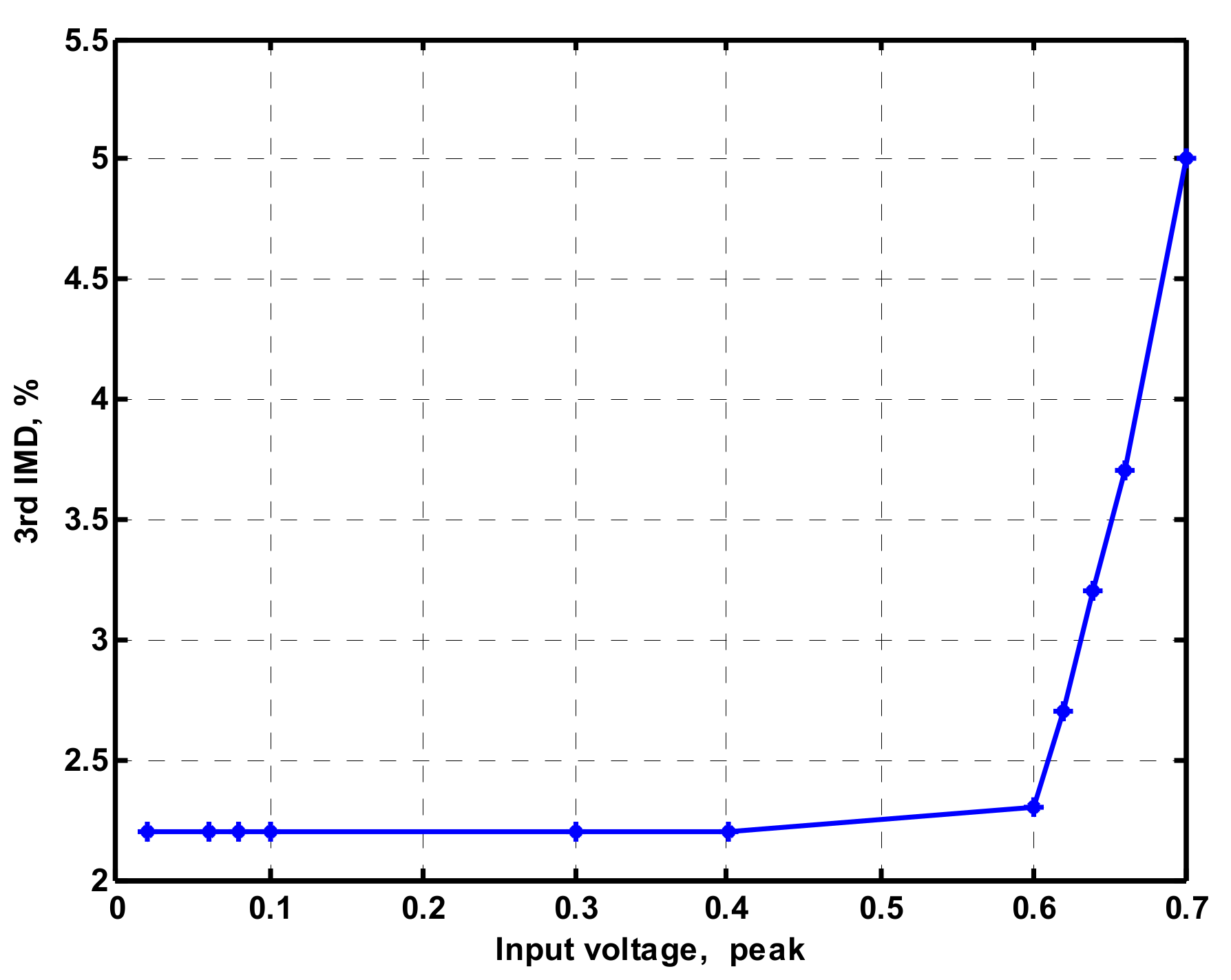
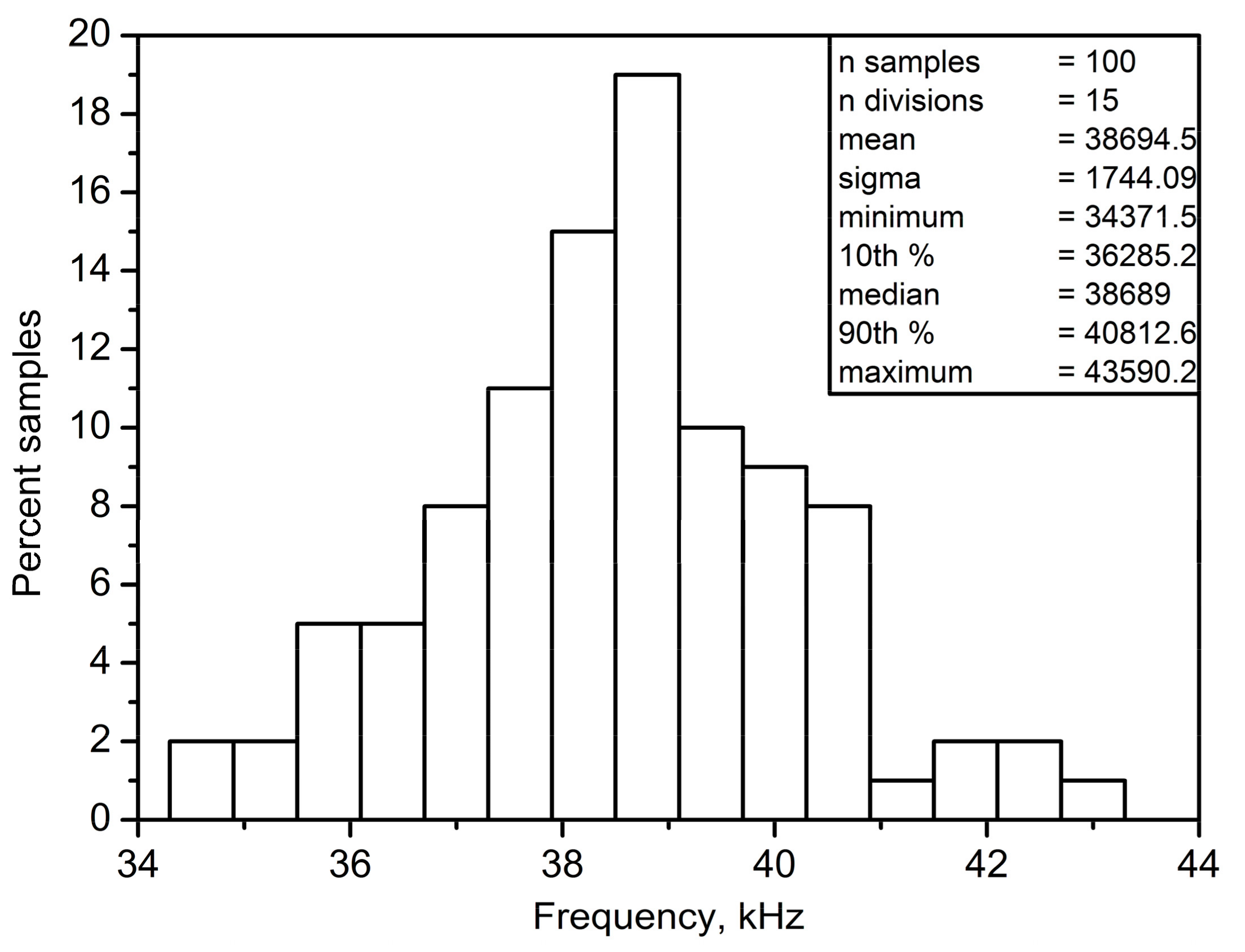
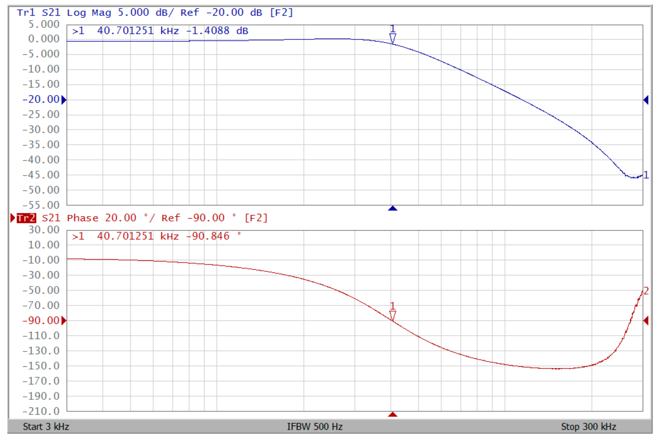
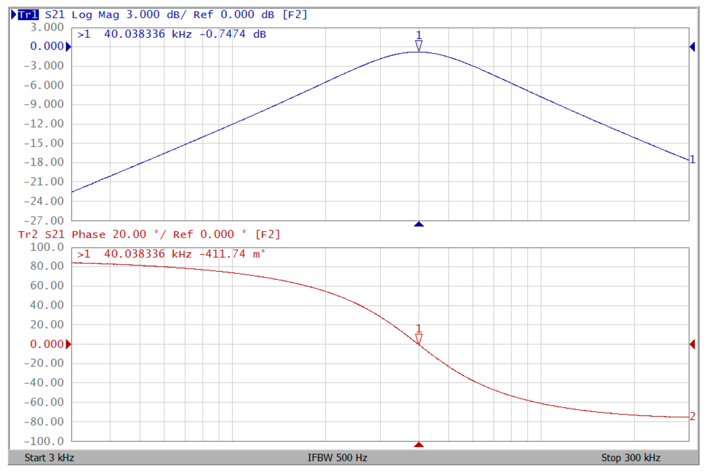
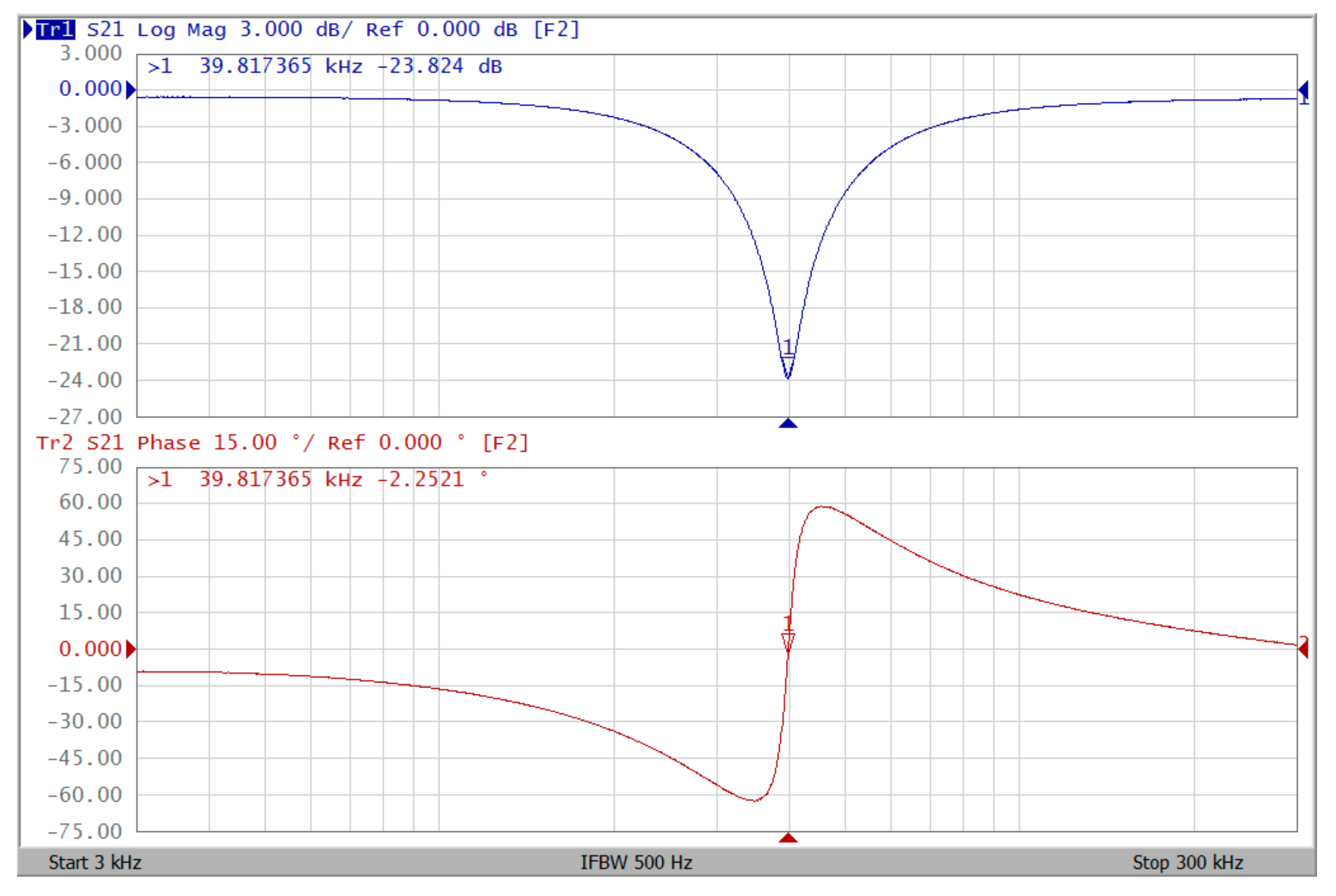
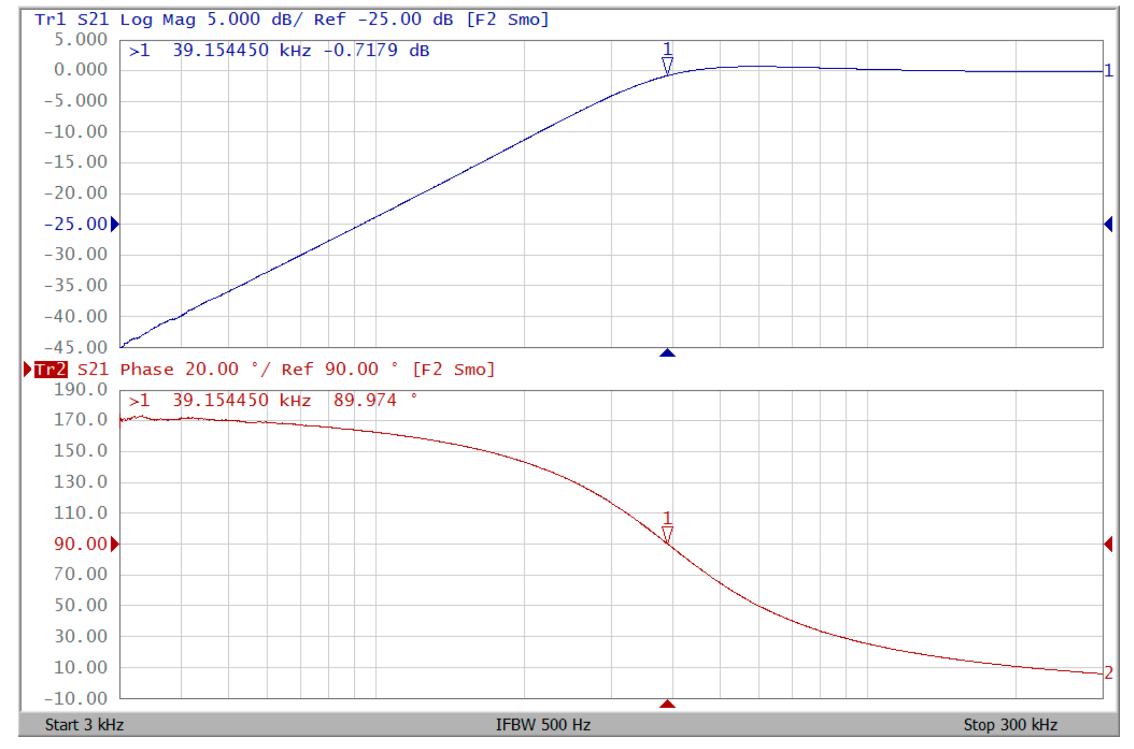
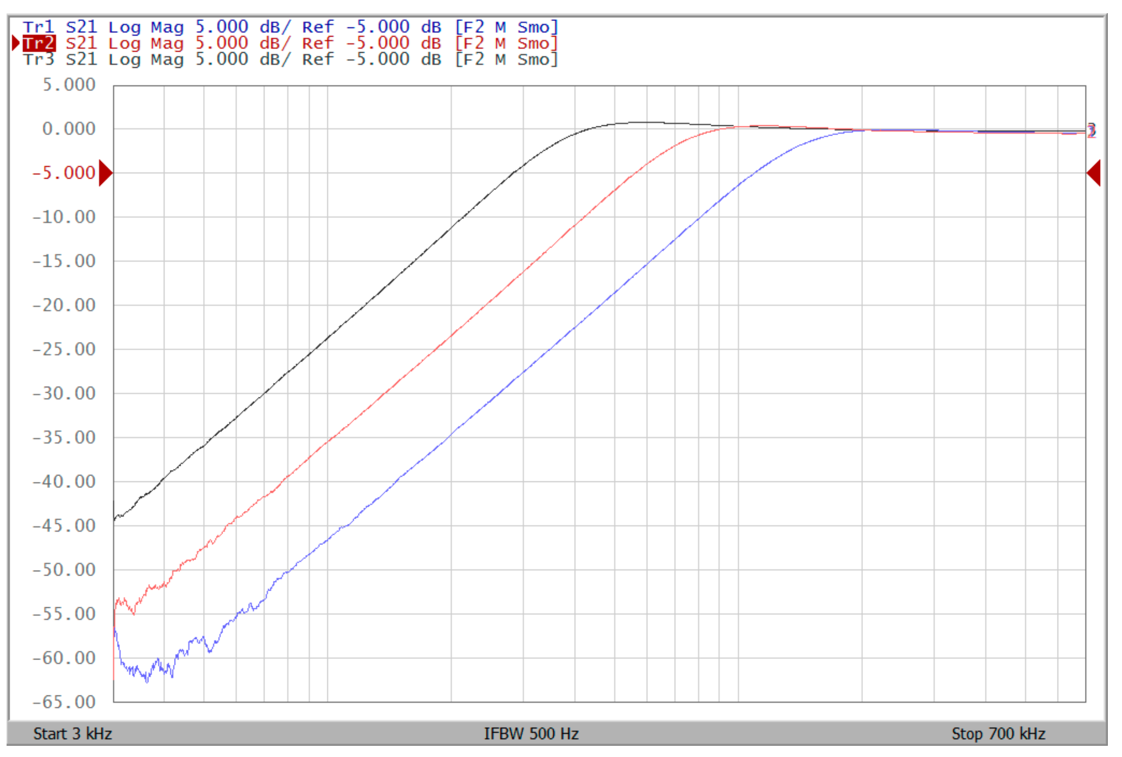
4. Simulation and Experimental Results

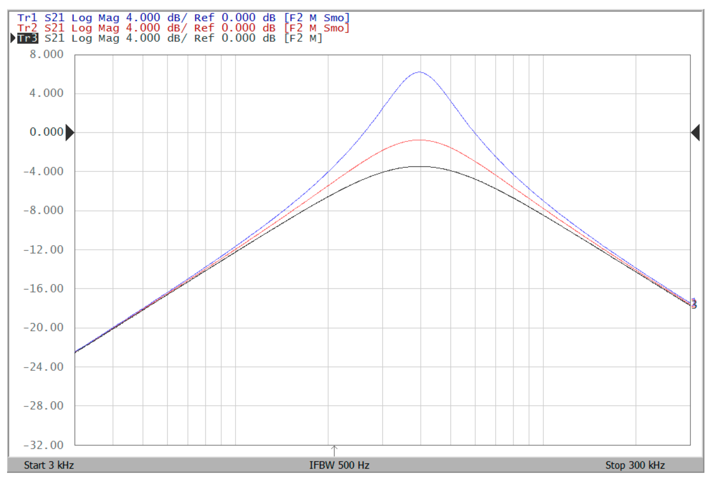
4.1. Voltage-Mode Multifunction Biquadratic Filter

The proposed CFOA-based filer was simulated using Cadence OrCAD PSpice (version 16.6, San Jose, CA, USA), and measured using the keysight E5061B-3L5 network analyzer (Santa Rosa, CA, USA), and Agilent N9000A CXA signal analyzer (Santa Rosa, CA, USA). The CFOAs were realized using the OrCAD PSpice macro-model of the AD844AN by Analog Devices as well as implemented in hardware using IC AD844AN [30]. The AD844AN supply voltages and capacitor values were selected as VDD = − VSS = 6V and C1 = C2 = 1 nF. Figure 7, Figure 8, Figure 9, Figure 10 and Figure 11 show the simulated and measured filtering responses with the equal resistors of R1 = R2 = R3 = 4 kΩ for Q = 1 and fo = 39.79 kHz, respectively. Figure 12 shows the variation in the angular frequency without affecting the quality factor. In Figure 12, equal resistors with R1 = R2 = R3 have different values of 4, 2, and 1 kΩ, resulting in Q = 1 for the HP filter and angular frequencies of fo = 39.79, 79.58, and 159.16 kHz, respectively. Next, the quality factor changes without affecting the angular frequency, as shown in Figure 13. This design is for an angular frequency of fo = 39.79 kHz with R2 = R3 = 4 kΩ and only varying the value of R1 as 5.6, 4, and 1.6 kΩ, resulting in Q = 0.71, 1, and 2.5 for the BP filter, respectively.
To test the input dynamic range of the proposed filter, the simulation of the IBP filter as an example was repeated for a sinusoidal input signal with fo = 39.79 kHz. Figure 14 shows the time-domain of the IBP response with Vi1 = 0 and Vi2 = Vin at the Vo1 output terminal, where all the resistor values are 4 kΩ. In Figure 14, the percentage of total harmonic distortion (THD) is 0.6%, when the sinusoidal input signal of an amplitude 1 VP at 39.79 kHz was applied. The dependence of the IBP filter output harmonic distortion on the input signal amplitude is shown in Figure 15. As can be seen in Figure 15, when the input signal amplitude increases by 2 Vp, its total harmonic distortion will increase by 3.2%. The intermodulation distortion (IMD) of the IBP response was studied. Figure 16 shows the dependence of the third-order IMD of IBP filter using two closely spaced tones, f1 = 38.79 kHz and f2 = 40.79 kHz, with equal input signal amplitude. The proposed filter was investigated using Monte-Carlo analysis. All the passive component deviations in the proposed filter were investigated using Monte-Carlo analysis. The Monte-Carlo simulations were performed on 100 samples. The Gaussian variations of all passive elements were 5%. Figure 17 shows a histogram of the angular frequencies obtained from the BP response Monte-Carlo analysis.
To demonstrate the validity of the theoretical analysis, the gain and phase responses obtained through the keysight E5061B-3L5 network analyzer are depicted in Figure 18, Figure 19, Figure 20, Figure 21 and Figure 22, respectively. In Figure 18, Figure 19, Figure 20, Figure 21 and Figure 22, the theoretical quality factor was Q = 1 and theoretical angular frequency was fo = 39.79 kHz, when the passive elements were set as C1 = C2 = 1 nF and R1 = R2 = R3 = 4 kΩ. The power consumption was approximately 180 mW under ± 6 V of supply voltages and 15 mA constant output current. In Figure 23, the measured values of angular frequency were equal to 39.15 kHz, 76.34 kHz, and 142.21 kHz, respectively, by adopting C1 = C2 = 1 nF and equal resistors of R1 = R2 = R3 with 4 kΩ, 2 kΩ, 1 kΩ. Selecting R2 = R3 = 4 kΩ and different values for R1 as 5.6, 4, and 1.6 kΩ, results in BP filters with theoretical angular frequency fo = 39.79 kHz and quality factors of Q = 0.71, 1, and 2.5, respectively, as shown in Figure 24. The measured values of Q were equal to 0.89, 1.06, and 2.12, respectively.
To represent the linearity of proposed filter, the 1 dB power gain compression point (P1dB) is measured through the Agilent N9000A CXA signal analyzer. Figure 25 shows the measured P1dB of the IBP filter with input power at the angular frequency of 39.79 kHz. As shown in Figure 25, the measured P1dB of the IBP filter at Vo1 is about 12 dBm with respect to input power. Figure 26 shows the spectrum of the IBP filter through inter-modulation characterization by applying two tone signals near 39.79 kHz with the amplitude of 1.15 Vp voltage. The result shows that the third-order IMD is around −31.08 dBc and the third-order intercept (TOI) is around 21.59 dBm.

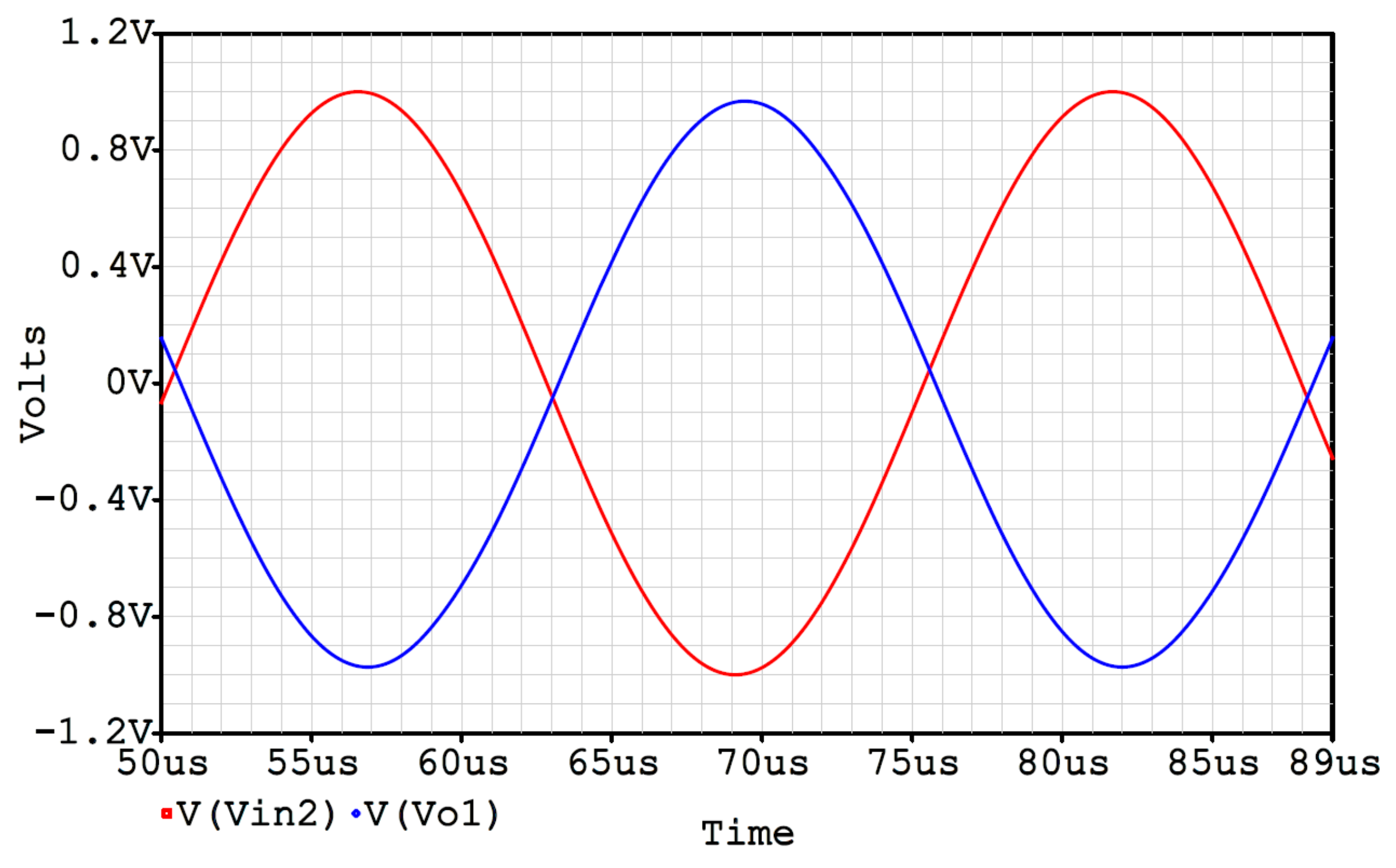
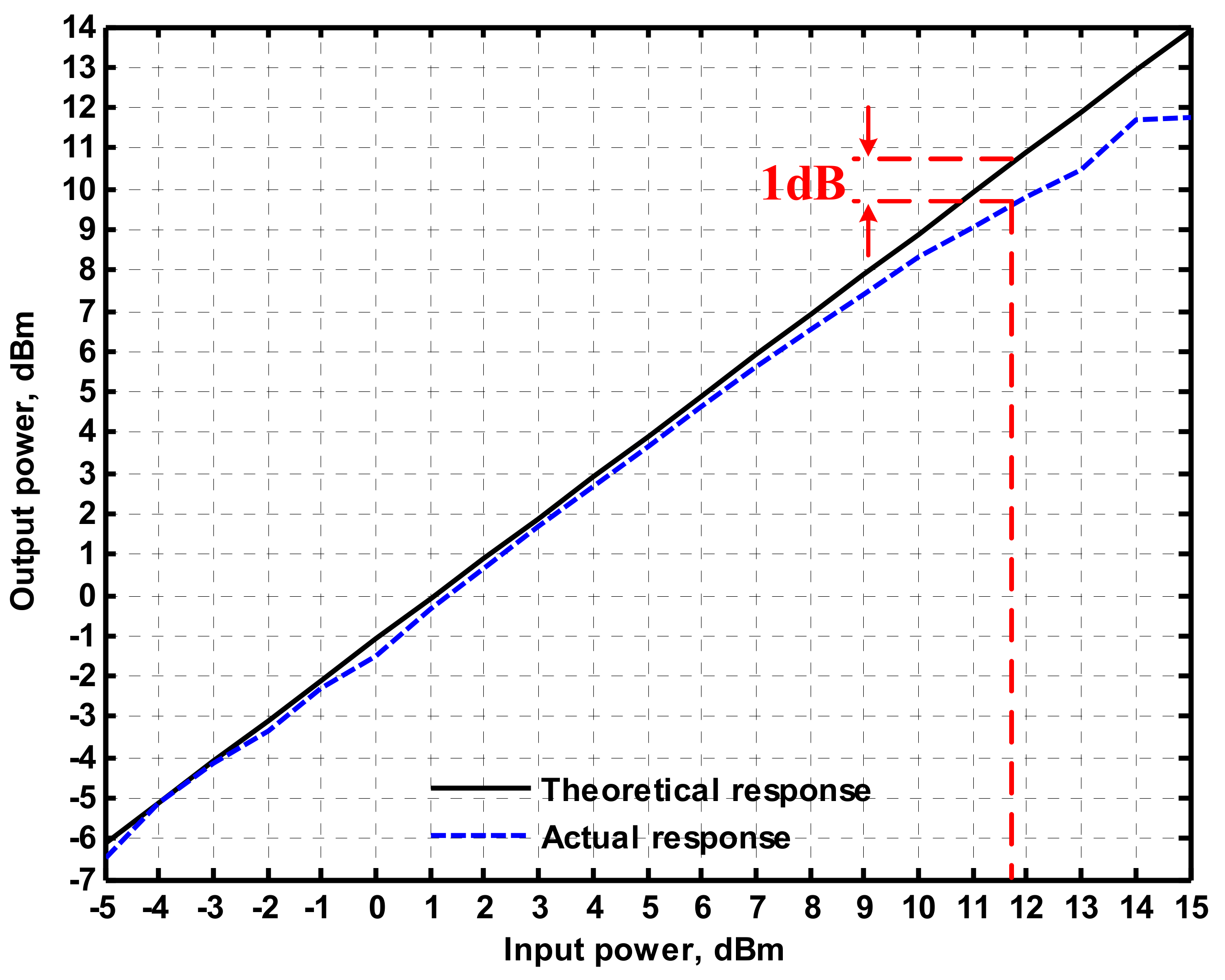
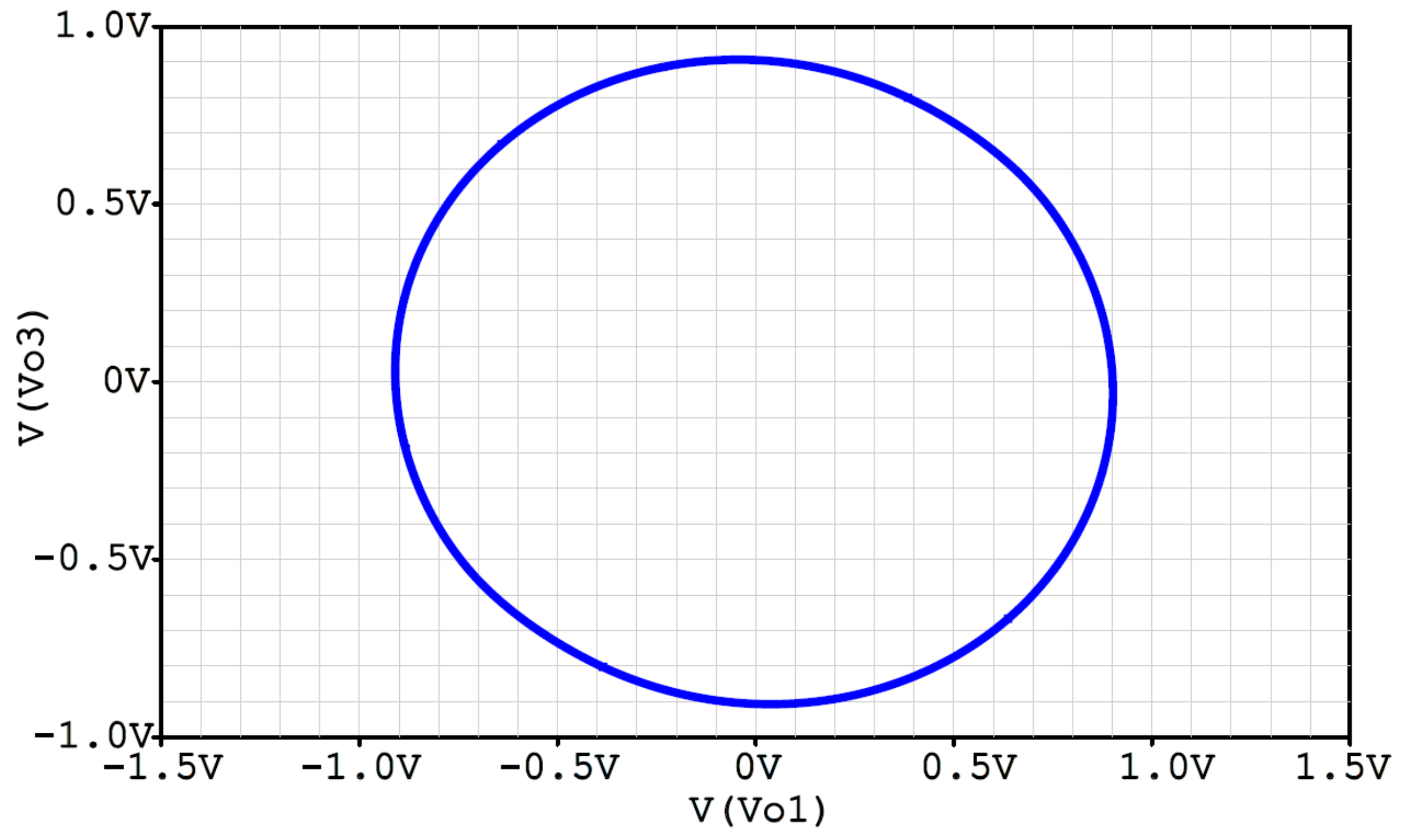
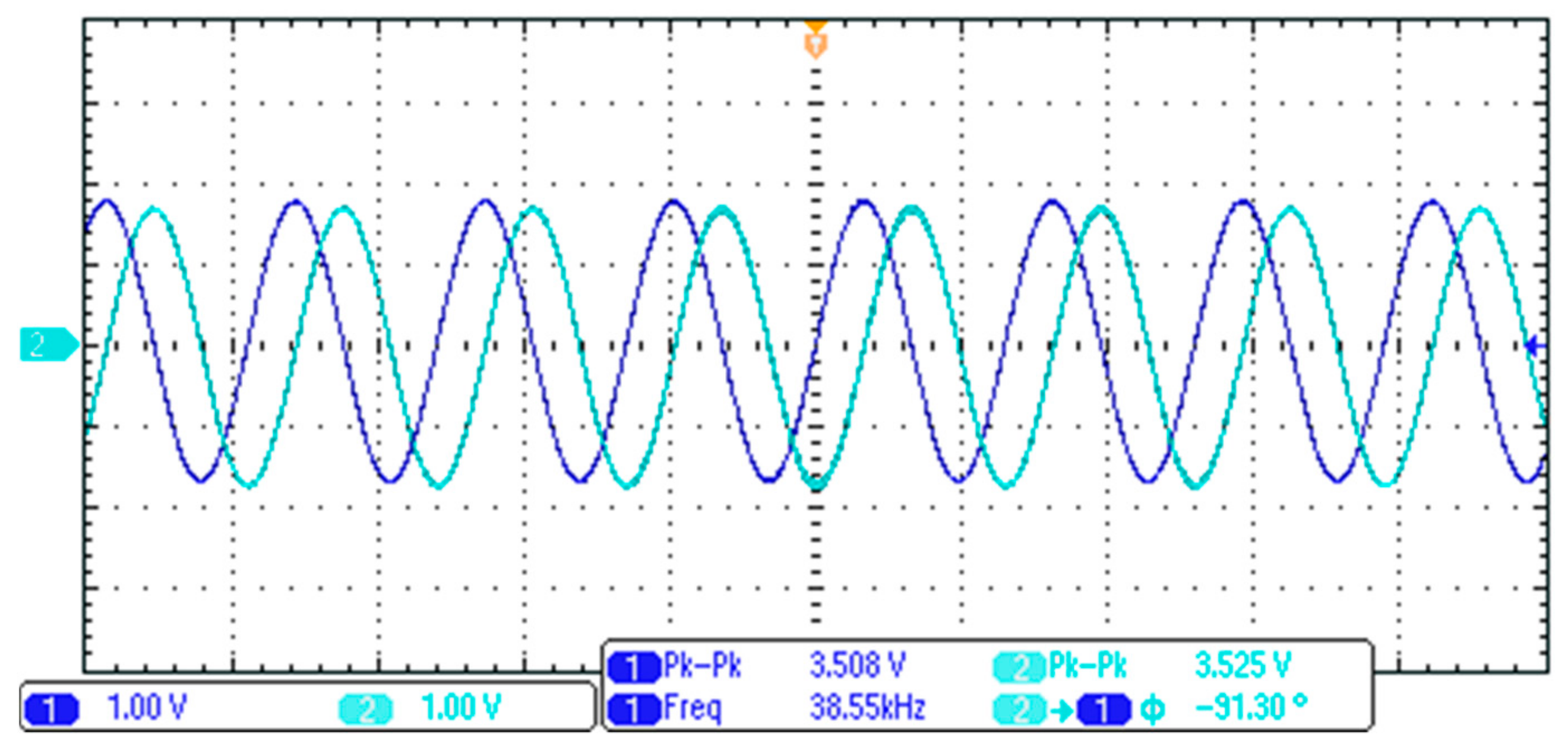
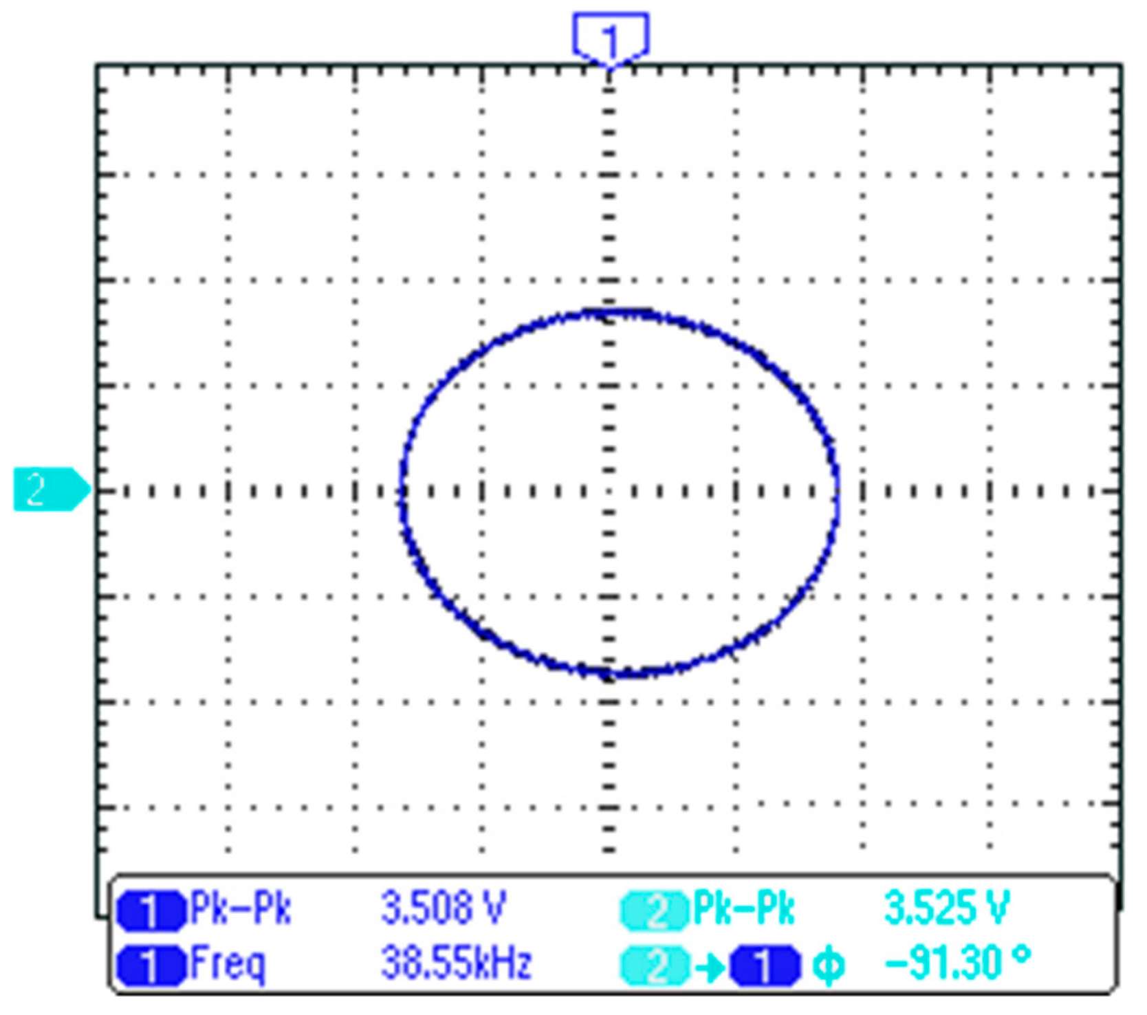
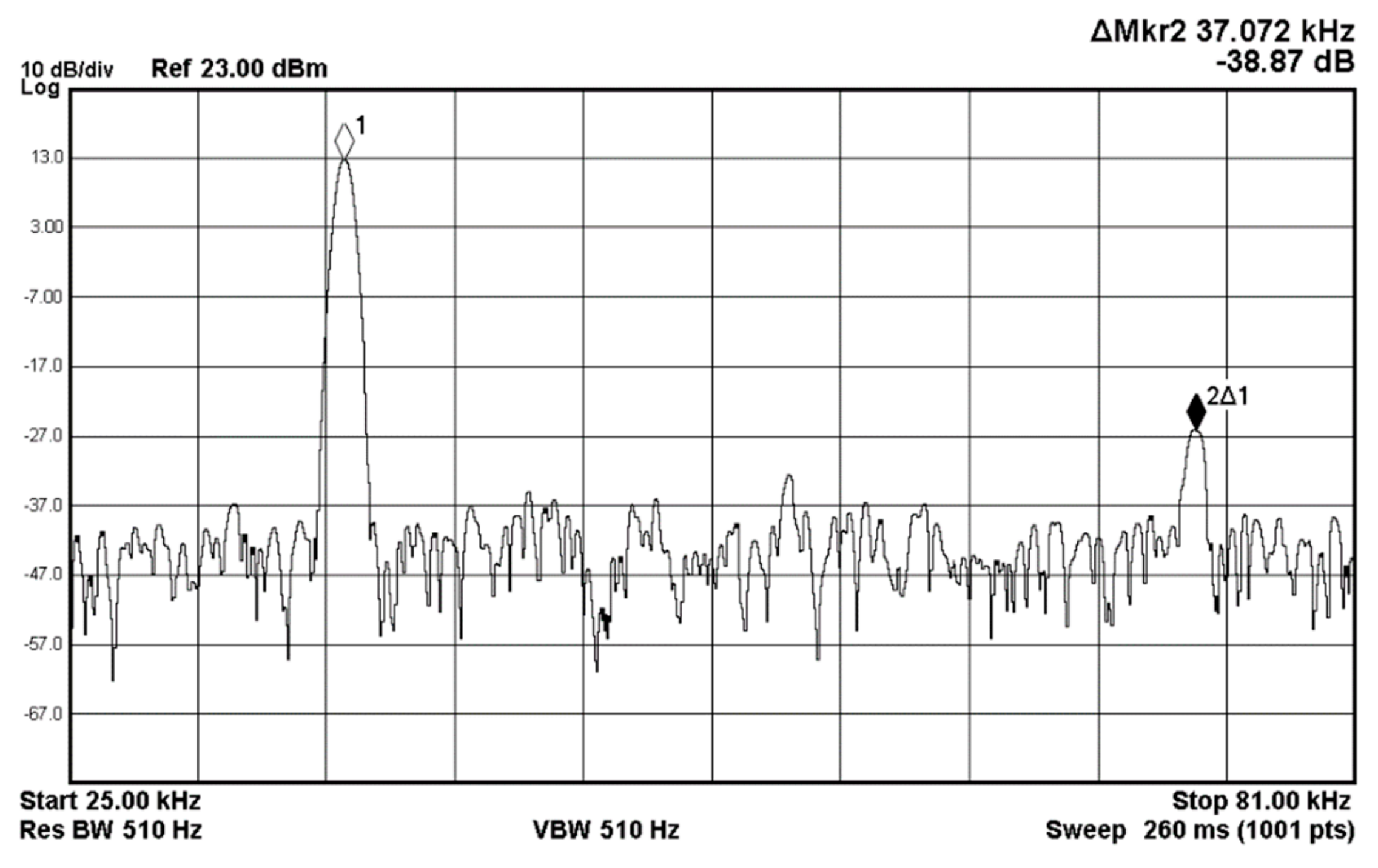
4.2. Voltage-Mode Quadrature Sinusoidal Oscillator

The proposed oscillator was simulated using OrCAD PSpice, and measured using the Agilent N9000A CXA signal analyzer. The supply voltages were VDD = −VSS = 6 V. The passive components were chosen as C1 = C2 = 1 nF and R1 = R2 = R3 = 4 kΩ. R4 was adjusted to 3.98 kΩ to start the oscillations. The theoretical oscillation frequency using this design was 39.79 kHz. The steady state waveforms for both the quadrature voltages are shown in Figure 27. Figure 28 shows the quadrature relationship between the generated waveforms of Vo1 and Vo3 in the X–Y plane. From the simulation results, the oscillation frequency of fo = 38.84 kHz was obtained, which agrees very well with the theoretical analysis The results of the Vo1 total harmonic distortion analysis are summarized in Table 3.
Regarding the experimental tests for the proposed oscillator, Figure 29 represents the oscilloscope output waveforms, Vo1 and Vo3, of the proposed oscillator in Figure 4. This is designed for the oscillation frequency of fo = 39.79 kHz with the component values of C1 = C2 = 1 nF and R1 = R2 = R3 = 4 kΩ, and the oscillation starts from R4 = 3.77 kΩ. The measured oscillation frequency, 38.55 kHz, is very close to theoretical value and the error is −3.12%. Figure 30 shows the Lissajous pattern of the Vo1 and Vo3 outputs of the experimental result in Figure 29. Figure 31 shows the frequency spectrum of the voltage output, Vo1, of the oscillator. The magnitude of the second harmonic is 38.87 dB less than the magnitude of the fundamental harmonic. The measured oscillation frequency, 37.072 kHz, is close to the theoretical value. Obviously, the experimental results are consistent with the theoretical values. Figure 32 shows how phase noise was calculated using the Agilent phase noise measurement solution. The phase noise in the proposed oscillator is lower than −85.7 dBc/Hz (at 1 kHz offset). Obviously, the experimental results are consistent with the theoretical values.

5. Conclusions

In this paper, a new two inputs and three outputs voltage-mode multifunction biquadratic filter with high-input impedances is presented. The proposed circuit uses three CFOAs, two grounded capacitors, and three resistors. All the X ports of the CFOAs in the proposed filter are connected directly to resistors. This design offers the feature of a direct incorporation of the parasitic resistance at the X terminal of the CFOA as a part of the main resistance. The circuit offers the advantage of orthogonal control of ωo and Q and simultaneously provides LP, BP, and BR responses while the IBP and HP responses can be easily obtained by applying another input voltage signal. Moreover, the filter can be easily converted into a quadrature oscillator, and the CO and the FO can be controlled independently. The experimental results validate that the functions of the proposed filter and oscillator are excellent.

Author Contributions

S.-F.W. and H.-P.C. conceived and designed the theoretical verifications; the optimization ideas were provided by Y.K.; H.-P.C. analyzed the results and wrote the paper; P.-Y.C. performed the simulations and experiments.

Funding

This research was funded by the Ming Chi University of Technology.

Acknowledgments

We are grateful to the editors and referees for their invaluable suggestions for improving the paper.

Conflicts of Interest

The authors declare no conflict of interest.

References

  1. Wang, H.Y.; Tran, H.D.; Nguyen, Q.M.; Yin, L.T.; Liu, C.Y. Derivation of oscillators from biquadratic band pass filters using circuit transformations. Appl. Sci. 2014, 4, 482–492. [Google Scholar] [CrossRef]
  2. Tran, H.D.; Wang, H.Y.; Lin, M.C.; Nguyen, Q.M. Synthesis of cascadable DDCC-based universal filter using NAM. Appl. Sci. 2015, 5, 320–343. [Google Scholar] [CrossRef]
  3. Chen, H.P.; Hwang, Y.S.; Ku, Y.T. Voltage-mode and current-mode resistorless third-order quadrature oscillator. Appl. Sci. 2017, 7, 179. [Google Scholar] [CrossRef]
  4. Chen, H.P.; Yang, W.S. Electronically tunable current controlled current conveyor transconductance amplifier-based mixed-mode biquadratic filter with resistorless and grounded capacitors. Appl. Sci. 2017, 7, 244. [Google Scholar] [CrossRef]
  5. Herencsar, N.; Koton, J.; Hanak, P. Universal voltage conveyor and its novel dual-output fully-cascadable VM APF application. Appl. Sci. 2017, 7, 307. [Google Scholar] [CrossRef]
  6. Sotner, R.; Jerabek, J.; Langhammer, L.; Dvorak, J. Design and analysis of CCII-Based oscillator with amplitude stabilization employing optocouplers for linear voltage control of the output frequency. Electronics 2018, 7, 157. [Google Scholar] [CrossRef]
  7. Ullah, F.; Liu, Y.; Li, Z.; Wang, X.; Sarfraz, M.M.; Zhang, H. A bandwidth-enhanced differential LC-voltage controlled oscillator (LC-VCO) and superharmonic coupled quadrature VCO for K-band applications. Electronics 2018, 7, 127. [Google Scholar] [CrossRef]
  8. Abuelma’atti, M.T.; Farooqi, A.A.; Alshahrani, S.M. Novel RC oscillators using the current-feedback operational amplifier. IEEE Trans. Circuits Syst. I Fund. Theory Appl. 1996, 43, 155–157. [Google Scholar] [CrossRef]
  9. Senani, R.; Bhaskar, D.R.; Singh, A.K.; Singh, V.K. Current feedback operational amplifiers and their applications. In Analog Circuits and Signal Processing; Springer: New York, NY, USA, 2013. [Google Scholar]
  10. Wang, C.; Zhang, J.; Wang, L.; Shi, W.; Jing, D. A novel Nth-order voltage-mode universal filter based on CMOS CFOA. Opt. Int. J. Light Electron Opt. 2016, 127, 2226–2230. [Google Scholar] [CrossRef]
  11. Mahmoud, S.A.; Madian, A.H.; Soliman, A.M. Low-voltage CMOS current feedback operational amplifier and its application. ETRI J. 2007, 29, 212–218. [Google Scholar] [CrossRef]
  12. Chen, H.P.; Wang, S.F.; Ku, Y.T.; Hsieh, M.Y. Quadrature oscillators using two CFOAs and four passive components. IEICE Electron. Express 2015, 12, 1–8. [Google Scholar] [CrossRef]
  13. Lahiri, A.; Jaikla, W.; Siripruchyanun, M. First CFOA-based explicit-current-output quadrature sinusoidal oscillators using grounded capacitors. Int. J. Electron. 2013, 100, 259–273. [Google Scholar] [CrossRef]
  14. Horng, J.W. Voltage-mode multifunction filter using one current feedback amplifier and one voltage follower. Int. J. Electron. 2001, 88, 153–157. [Google Scholar] [CrossRef]
  15. Liu, S.I.; Wu, D.S. New current-feedback amplifier-based universal biquadratic filter. IEEE Trans. Instrum. Meas. 1995, 44, 915–917. [Google Scholar]
  16. Horng, J.W. New Configuration for realizing universal voltage-mode filter using two current-feedback amplifiers. IEEE Trans. Instrum. Meas. 2000, 49, 1043–1045. [Google Scholar] [CrossRef]
  17. Shan, N.A.; Rather, M.F.; Iqbal, S.Z. CFA-based three input and two outputs voltage-mode universal filter. Indian J. Pure Appl. Phys. 2005, 43, 636–639. [Google Scholar]
  18. Shah, N.A.; Iqbal, S.Z.; Rather, M.F. Versatile voltage-mode CFA-based universal filter. AEU Int. J. Electron. Commun. 2005, 59, 192–194. [Google Scholar] [CrossRef]
  19. Tangsrirat, W.; Surakampontorn, W. Single-resistance-controlled quadrature oscillator and universal biquad filter using CFOAs. AEU Int. J. Electron. Commun. 2009, 63, 1080–1086. [Google Scholar] [CrossRef]
  20. Horng, J.W. Voltage-mode universal biquad with five inputs and two outputs using two current feedback amplifiers. Indian J. Eng. Mater. Sci. 2013, 20, 87–91. [Google Scholar]
  21. Nikoloudis, S.; Psychalinos, C. Multiple input single output universal biquad filter with current feedback operational amplifiers. Circuits Syst. Signal Process. 2010, 29, 1167–1180. [Google Scholar] [CrossRef]
  22. Topaloglu, S.; Sagbas, M.; Anday, F. Three-input single-output second-order filters using current-feedback amplifiers. AEU Int. J. Electron. Commun. 2012, 66, 683–686. [Google Scholar] [CrossRef]
  23. Minaei, S.; Ibragun, M.A. A mixed-mode KHN-biquad using DVCC and grounded passive elements suitable for direct cascading. Int. J. Circuit Theory Appl. 2009, 37, 793–810. [Google Scholar] [CrossRef]
  24. Singh, V.K.; Singh, A.K.; Bhaskar, D.R.; Senani, R. New universal biquads employing CFOAs. IEEE Trans. Circuits Syst. II Express Briefs 2006, 53, 1299–1303. [Google Scholar] [CrossRef]
  25. Ibrahim, M.A.; Minaei, S.; Kuntman, H. A 22.5MHzcurrent-mode KHN biquad using differential voltage current conveyor and grounded passive element. AEU Int. J. Electron. Commun. 2005, 59, 311–318. [Google Scholar] [CrossRef]
  26. Chang, C.M.; Hwang, C.S.; Tu, S.H. Voltage-mode notch, lowpass and bandpass filter using current-feedback amplifiers. Electron. Lett. 1994, 30, 2002–2003. [Google Scholar] [CrossRef]
  27. Horng, J.W.; Lee, M.H. High input impedance voltage-mode lowpass, bandpass and highpass filter using current-feedback amplifiers. Electron. Lett. 1997, 33, 947–948. [Google Scholar] [CrossRef]
  28. Shan, N.A.; Malik, M.A. High input impedance voltage-mode lowpass, bandpass, highpass and notch filter using current feedback amplifiers. Indian J. Eng. Mater. Sci. 2005, 12, 278–280. [Google Scholar]
  29. Shan, N.A.; Malik, M.A. New high input impedance voltage-mode lowpass, bandpass and highpass filter using current feedback amplifiers. J. Circuits Syst. Comp. 2005, 14, 1037–1043. [Google Scholar]
  30. AD844: 60 MHz, 2000 V/μs, Monolithic Op Amp with Quad Low Noise Data Sheet (Rev. G). May 2017. Available online: www.linear.com. (accessed on 29 April 2019).
Figure 1. Schematic symbol of CFOA.
Applsci 09 02304 g001
Figure 2. Implementation of CFOA given by a CCII+ and a VB.
Applsci 09 02304 g002
Figure 3. The proposed high-input impedance CFOA-based multifunction biquadratic filter.
Applsci 09 02304 g003
Figure 4. The proposed quadrature sinusoidal oscillator using the filter in Figure 3.
Applsci 09 02304 g004
Figure 5. General equivalent circuit of the non-ideal CFOA.
Applsci 09 02304 g005
Figure 6. Proposed voltage-mode biquadratic filter including the parasitic elements of CFOA.
Applsci 09 02304 g006
Figure 7. Simulation and experimental results of LP filtering responses at Vo1 when Vi1 = Vin and Vi2 = 0.
Applsci 09 02304 g007
Figure 8. Simulation and experimental results of BP filtering responses at Vo2 when Vi1 = Vin and Vi2 = 0.
Applsci 09 02304 g008
Figure 9. Simulation and experimental results of BR filtering responses at Vo3 when Vi1 = Vin and Vi2 = 0.
Applsci 09 02304 g009
Figure 10. Simulation and experimental results of IBP filtering responses at Vo1 when Vi1 = 0 and Vi2 = Vin.
Applsci 09 02304 g010
Figure 11. Simulation and experimental results of HP filtering responses at Vo3 when Vi1 = 0 and Vi2 = Vin.
Applsci 09 02304 g011
Figure 12. Simulation and experimental results of HP filtering responses at Vo3 when Vi1 = 0 and Vi2 = Vin.
Applsci 09 02304 g012
Figure 13. Simulation and experimental results of BP filtering responses at Vo2 when Vi1 = Vin and Vi2 = 0.
Applsci 09 02304 g013
Figure 14. Time domain response of the IBP filter at Vo1 when Vi1 = 0 and Vi2 = Vin.
Applsci 09 02304 g014
Figure 15. Dependence of output harmonic distortion of the IBP filter on an input signal amplitude.
Applsci 09 02304 g015
Figure 16. Dependence of the third-order IMD of the IBP filter on input signal amplitudes.
Applsci 09 02304 g016
Figure 17. Histogram of Monte-Carlo sensitivity analysis of BP filter at Vo2 when Vi1 = Vin and Vi2 = 0.
Applsci 09 02304 g017
Figure 18. Measured gain and phase responses at Vo1 when Vi1 = Vin and Vi2 = 0.
Applsci 09 02304 g018
Figure 19. Measured gain and phase responses at Vo2 when Vi1 = Vin and Vi2 = 0.
Applsci 09 02304 g019
Figure 20. Measured gain and phase responses at Vo3 when Vi1 = Vin and Vi2 = 0.
Applsci 09 02304 g020
Figure 21. Measured gain and phase responses at Vo1 when Vi1 = 0 and Vi2 = Vin.
Applsci 09 02304 g021
Figure 22. Measured gain and phase responses at Vo3 when Vi1 = 0 and Vi2 = Vin.
Applsci 09 02304 g022
Figure 23. Measured gain responses of HP (Vo3) filters by varying fo while keeping Q (fo = 39.15 kHz—black line; fo = 76.34 kHz—red line; and fo = 142.21 kHz—blue line).
Applsci 09 02304 g023
Figure 24. Measured gain responses of BP (Vo2) filters by varying Q while keeping fo (Q = 0.89—black line; Q = 1.06—red line; and Q = 2.12—blue line).
Applsci 09 02304 g024
Figure 25. Measured P1dB of the IBP filter with input power at Vo1 when Vi1 = 0 and Vi2 = Vin.
Applsci 09 02304 g025
Figure 26. Measured IBP filter of the two-tone test with the amplitude of 1.15 VP voltage.
Applsci 09 02304 g026
Figure 27. Simulated quadrature output waves Vo1 (blue) and Vo3 (red) of Figure 4.
Applsci 09 02304 g027
Figure 28. Simulated quadrature output waves Vo1 and Vo3 in the X–Y plane of Figure 27.
Applsci 09 02304 g028
Figure 29. Experimental of the quadrature outputs time-domain results Vo1 (blue) and Vo3 (cyan).
Applsci 09 02304 g029
Figure 30. Lissajous pattern of Vo1 and Vo3 outputs in Figure 29 (horizontal scale: 1 V/div; vertical scale: 1 V/div).
Applsci 09 02304 g030
Figure 31. Measured frequency spectrum of Vo1.
Applsci 09 02304 g031
Figure 32. Measured phase noise of the proposed oscillator in Figure 4.
Applsci 09 02304 g032
Table 1. Comparison of the proposed circuit with previously CFOA-based multifunction biquadratic filters in the literature [26,27,28,29].
Parameter(i)(ii)(iii)(iv)(v)(vi)(vii)
Reference [26]yesnonoyesyesyesno
Reference [27]nonoyesyesyesyesno
Reference [28]noyesyesyesyesyesno
Reference [29]nonoyesnonoyesno
Proposedyesyesyesyesyesyesyes
Table 2. Two inputs and three outputs filtering functions realized.
Input ConditionsOutput TerminalsFilter FunctionsPassband Gains
Only Vi1 as input signalVo1non-inverting low-passunity
Vo2non-inverting band-pass R 3 R 1
Vo3non-inverting band-rejectunity
Only Vi2 as input signalVo1inverting band-pass C 2 R 2 C 1 R 1
Vo2nonenone
Vo3non-inverting high-pass R 1 R 3
Table 3. Total harmonic distortion analysis of Vo1 in Figure 4.
Harmonic
Number
Frequency
(Hz)
Fourier
Component
Normalized
Component
Phase
(Degree)
Normalized
Phase (Degree)
13.98 × 1048.94 × 10−11.007.94 × 1010
27.96 × 1041.45 × 10−21.62 × 10−26.74 × 101−9.14 × 101
31.19 × 1057.03 × 10−37.86 × 10−36.90 × 101−1.69 × 10²
41.59 × 1053.28 × 10−33.66 × 10−35.23 × 101−2.65 × 10²
51.99 × 1052.49 × 10−32.78 × 10−34.31 × 101−3.54 × 10²
62.39 × 1051.88 × 10−32.11 × 10−34.71 × 101−4.29 × 10²
72.79 × 1051.38 × 10−31.54 × 10−33.14 × 101−5.24 × 10²
83.18 × 1051.19 × 10−31.33 × 10−32.85 × 101−6.07 × 10²
93.58 × 1059.40 × 10−41.05 × 10−33.52 × 101−6.79 × 10²
DC component = −2.560956 × 10⁻²
Total harmonic distortion = 1.887184%

