Article

Characterization of Trap States in AlGaN/GaN MIS-High-Electron-Mobility Transistors under Semi-on-State Stress

1
School of Advanced Technology, Xi’an Jiaotong-Liverpool University, Suzhou 215123, China
2
Department of Electrical Engineering and Electronics, University of Liverpool, Liverpool L69 3GJ, UK
3
Department of Communications and Networking, Xi’an Jiaotong-Liverpool University, Suzhou 215123, China
4
School of Chips, Entrepreneur College (Taicang), Xi’an Jiaotong-Liverpool University, Suzhou 215123, China
*
Authors to whom correspondence should be addressed.
Nanomaterials 2024, 14(18), 1529; https://doi.org/10.3390/nano14181529
Submission received: 21 August 2024 / Revised: 16 September 2024 / Accepted: 19 September 2024 / Published: 20 September 2024
(This article belongs to the Special Issue Epitaxial Growth of III-Nitride Hetero- and Nanostructures)

Abstract

:
Devices under semi-on-state stress often suffer from more severe current collapse than when they are in the off-state, which causes an increase in dynamic on-resistance. Therefore, characterization of the trap states is necessary. In this study, temperature-dependent transient recovery current analysis determined a trap energy level of 0.08 eV under semi-on-state stress, implying that interface traps are responsible for current collapse. Multi-frequency capacitance–voltage (C-V) testing was performed on the MIS diode, calculating that interface trap density is in the range of 1.37 × 10 13 to 6.07 × 10 12 cm 2 eV 1 from E C E T = 0.29 eV to 0.45 eV.

1. Introduction

GaN-based devices are suitable for high-voltage and high-switching applications due to their wide bandgap and high carrier mobility of two-dimensional electron gas (2DEG) [1]. AlGaN/GaN high-electron-mobility transistors (HEMTs) suffer from current collapse, especially under high-drain bias in the off-state, due to surface defects related to N-vacancies [2].
There are some works dedicated to suppressing current collapse using physical methods, such as ECR N 2 -plasma pre-treatment [2] and oxygen plasma treatment [3], or through structural optimization methods, such as the bi-passivation layer [4] and the fluorinated graphene passivation layer [5]. Some studies have found that Si3N4 can passivate the N-vacancies on the surface of AlGaN. However, it is not suitable as a gate-insulating layer due to its small band offset with AlGaN (bandgap EG of Si3N4 is approximately 5 eV; in comparison, the EG of AlGaN is approximately 4.1 eV) and relatively low dielectric constant ( ϵ r ∼7.5) [2]. Thus, many studies have proposed Al2O3 (EG∼7 eV and ϵ r ∼9.3) as a gate dielectric and passivation layer [3,4,5,6,7,8,9,10,11]. These studies investigate the degradation mechanism under off-state stress in the device [2,3,4,5,11]; however, they rarely focus on the degradation under semi-on-state stress.
The semi-on-state stress condition is typically defined as a gate voltage higher than the threshold voltage but not exceeding two volts [12,13,14,15]. In this state, the drain voltage is always maintained at a high level, the average energy of the electrons is measured in terms of electron temperature (Te), the Te increases correspondingly, and the positions of hot spots also change [16]. Electron trapping could occur in the AlGaN barrier [17], the oxide layer, at the interface [13], or in the buffer layer [18]. This can lead to more severe current collapse or on-resistance degradation compared to off-state stress.
This study investigates the current collapse of AlGaN/GaN MIS-HEMTs with 20 nm Al2O3 as the gate dielectric and passivation under the semi-on and off-states by employing pulse I–V testing. Moreover, temperature-dependent transient recovery current tests and Arrhenius plots are performed to obtain the emission time constants and calculate the energy levels of interface traps associated with semi-on-state stress. Multi-frequency capacitance–voltage (C-V) testing was performed on the MIS diode to calculate interface trap density.
This article is organized into four sections. Section 2 describes the fabrication process of the device and its static characteristics. Section 3 presents the current collapse results of the device under semi-on and off-states, as tested by the pulse I–V method. Section 4 discusses the electron trapping mechanisms and calculates the energy levels and density of the interface traps. Conclusions are drawn in Section 5.

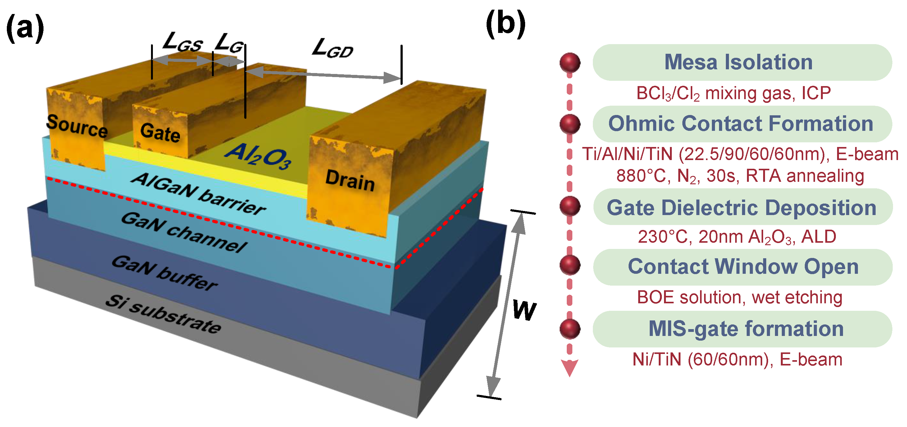
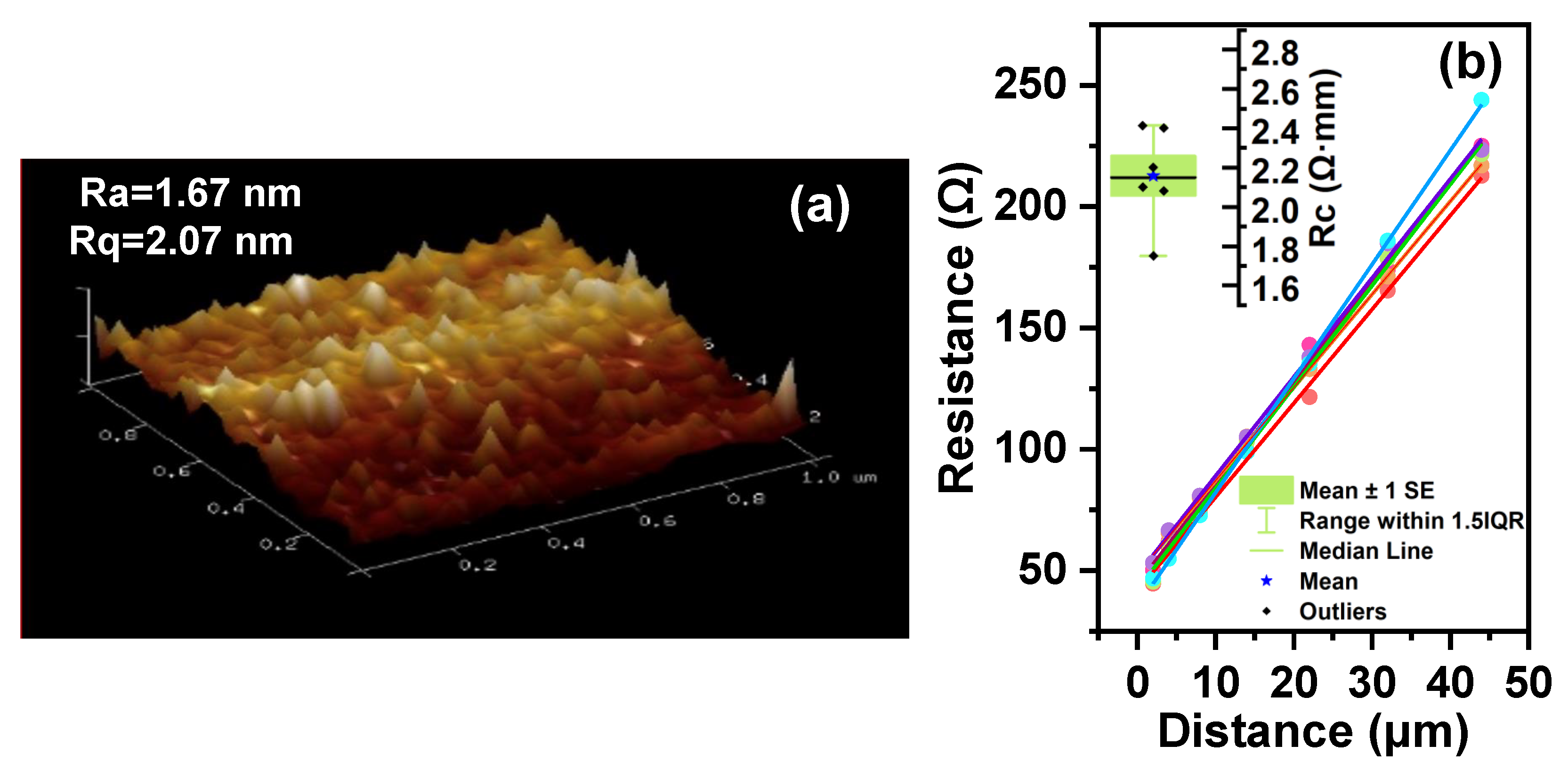
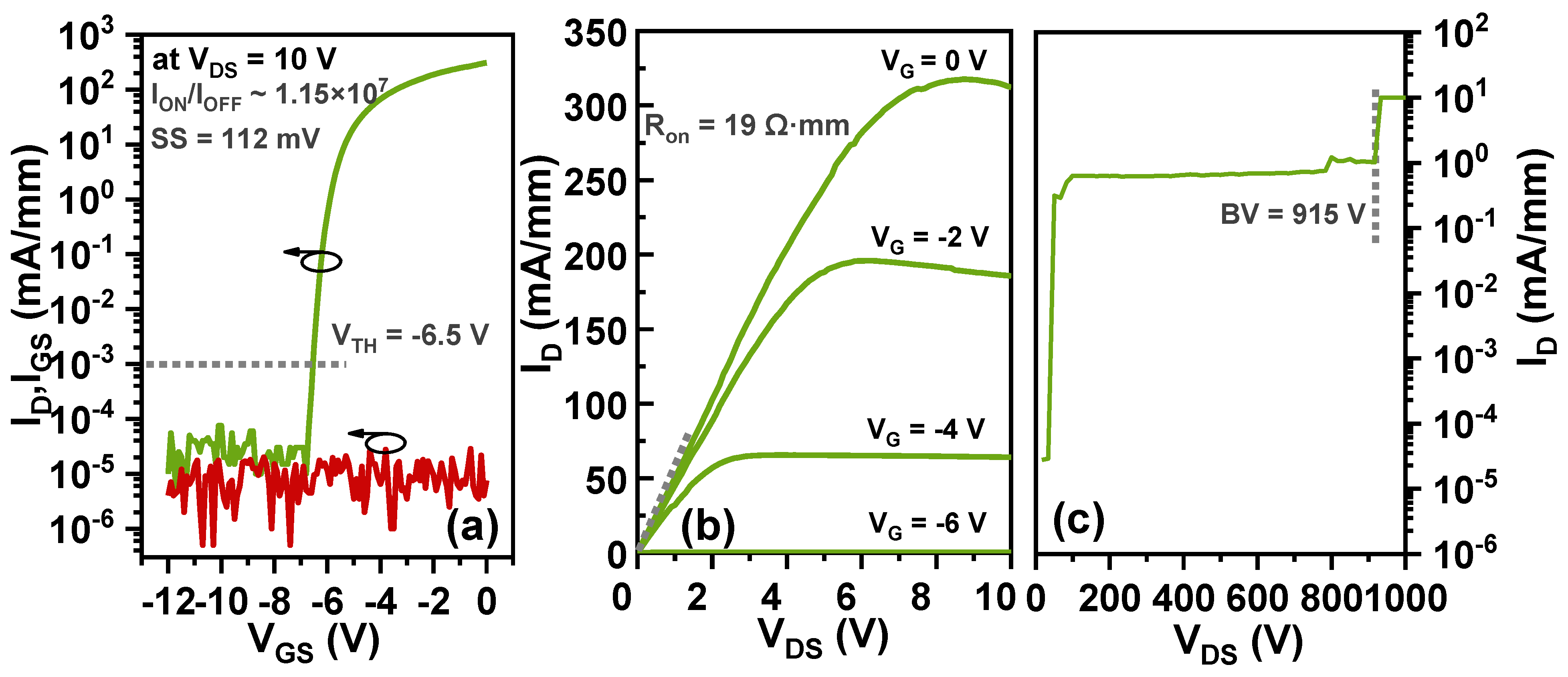
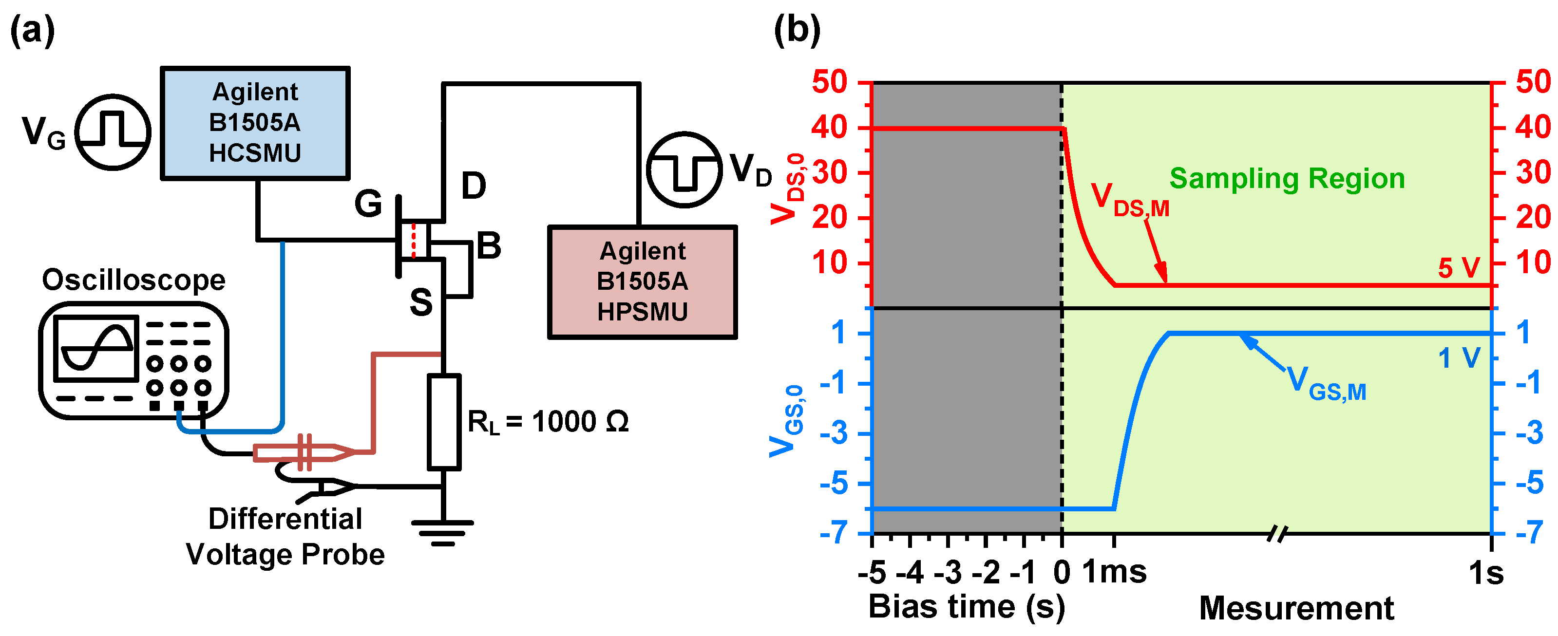
2. Device Fabrication and Characterization

The simplified schematic structure of the AlGaN/GaN MIS-HEMTs, which was analyzed in this research, is depicted in Figure 1a, while the fabrication process is shown in Figure 1b. The devices are fabricated on a commercially available epitaxial wafer supplied by Enkris Semiconductor, Inc., Suzhou, China, with a sheet carrier density of 1 × 10 13 cm 2 . The wafer consisted of several layers: a 23 nm undoped Al 0.25 Ga 0.75 N barrier layer, a 330 nm GaN channel layer, and a 5 μm undoped GaN buffer layer, all grown on the Si substrate.
The fabrication process starts with the mesa isolation step, achieved by an inductively coupled plasma (ICP) dry-etching system. The etching rate is 16 nm/min. The etching gas flow rates are Cl 2 / BCl 3 = 4/10 sccm, with the ICP power set at 50 W and the radio frequency (RF) power set at 30 W. A 350 nm PECVD-Si3N4 layer is used as a hard mask to protect the access region. After the etching process, the etched height is approximately 350 nm, with an average surface roughness (Ra) of 1.67 nm and a root mean square roughness (Rq) of 2.07 nm, as measured by atomic force microscopy (AFM), as shown in Figure 2a. To reduce leakage current and minimize native oxide and nitrogen vacancies at the GaN surface, the samples are immersed in an 80 °C tetramethylammonium hydroxide (TMAH) solution for 5 min.
Next, a metal stack of Ti/Al/Ni/TiN (22.5/90/60/60 nm) is evaporated using an electron-beam (E-beam) evaporation system. Then, the metal stack is annealed at 880 °C in an N2 atmosphere for 30 s to form the N-type ohmic contact. The contact resistances (Rc) are measured using the transmission line model (TLM) by assessing the resistance between pairs of contacts with different spacings of 2, 4, 8, 14, 22, 32, and 44 μm [19]. As shown in Figure 2b, the average contact resistance is 2.1 Ω ·mm, with a sheet resistance of 383 Ω /sqr.
Before the Al2O3 deposition, the samples were immersed in a 10% HCl solution for 1 min. After that, a 20 nm Al2O3 is deposited using the atomic layer deposition (ALD) system as the gate dielectric and passivation layer. In the ALD system, tetramethylaluminum (TMA) provides the aluminum source, while H2O provides the oxygen source, with pulse time of 50 ms and 40 ms, respectively. The deposition temperature is 230 °C, and the chamber pressure is 12 Pa. The deposition rate is 0.08 nm/cycle. The buffer oxide etch (BOE) solution is used to wet-etch the Al2O3 layer above the source and drain contact regions.
Finally, a Ni/TiN (60/60 nm) metal stack is evaporated as the gate electrode. The device dimensions are as follows: the distance between the source and drain ( L S D ) is 28 μm; the distance between the gate and source ( L G S ) is 5 μ m; the gate length ( L G ) is 3 μ m; the distance between the gate and drain ( L G D ) is 20 μ m; and the device width (W) is 100 μ m.
Figure 3a,b illustrate the device’s static transfer and output characteristics by Agilent B1505A Medium Power Source Monitor Unit (MPSMU) and High-Power-Source Monitor Unit (HPSMU). In Figure 3a, the gate voltage sweeps from −12 V to 0 V with a step of 0.5 V, the tested device exhibits a satisfactory I O N / I O F F ratio of 1.15 × 10 7 , a low gate leakage current level of 10 4 to 10 6 mA/mm, a subthreshold voltage swing (SS) of 112 mV, and a threshold voltage ( V T H ) of −6.5 V at a drain current criterion of 1 μ A/mm. In Figure 3b, the gate voltage increases from −12 V to 0 V in steps of 2 V, while the drain voltage sweeps from 0 V to 10 V in steps of 0.5 V. The drain current is 310 mA/mm at a gate voltage ( V G S ) of 0 V, and a drain voltage ( V D S ) of 10 V. The static on-resistance ( R O N , S ) is 19 Ω ·mm at a gate voltage ( V G S ) of 0 V, and a drain voltage ( V D S ) of 0.1 V.
In Figure 3c, the MPSMU provides the gate voltage, and the High-Voltage-Source Monitor Unit (HVSMU) provides the drain voltage. The gate voltage remains at −8 V (off-state), while the drain voltage increases from 0 V to 1000 V in steps of 5 V. The drain voltage at which a sudden increase in current occurs is called the breakdown voltage. The breakdown voltage (BV) of the device is 915 V at V G S of −8 V with a floating substrate.

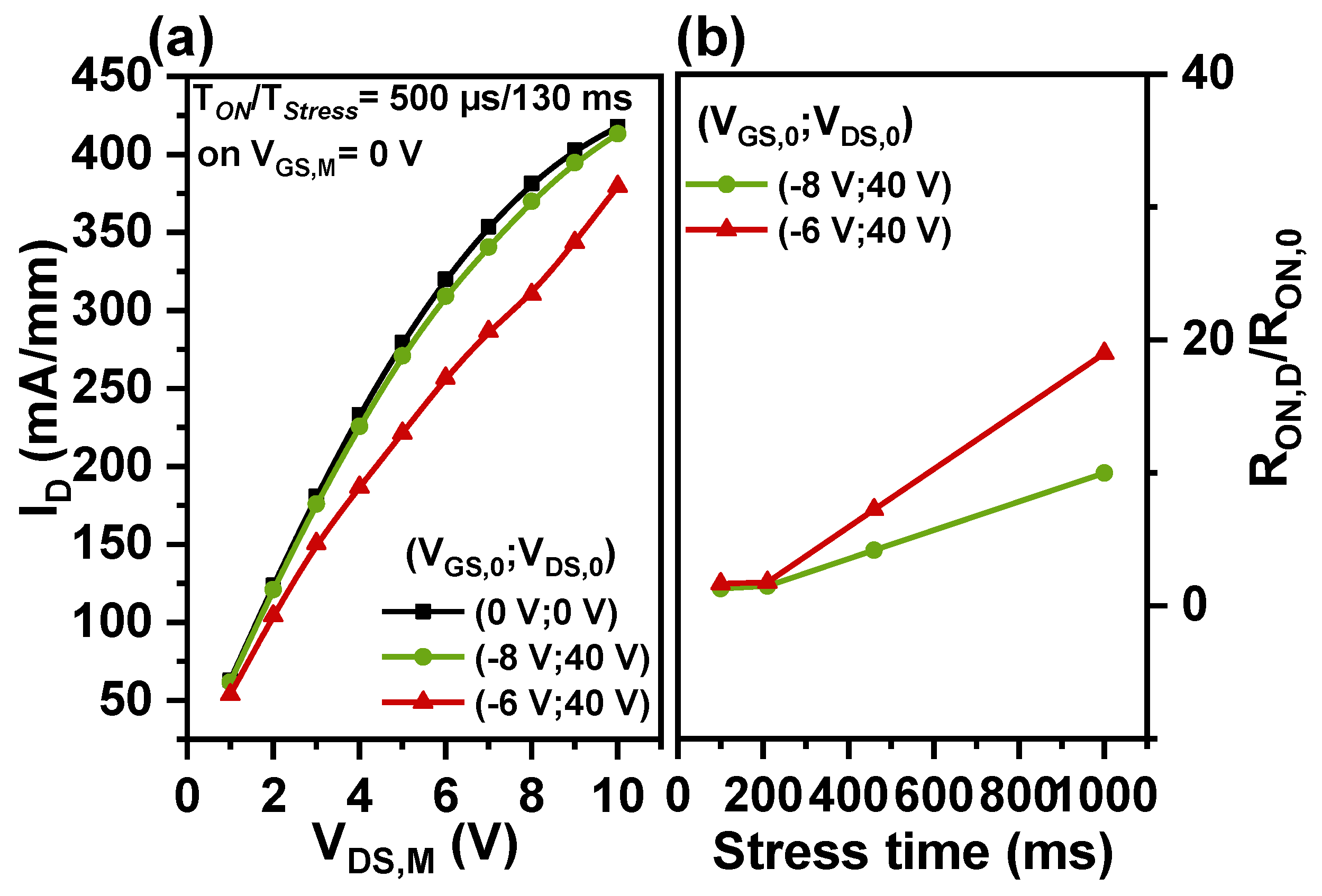
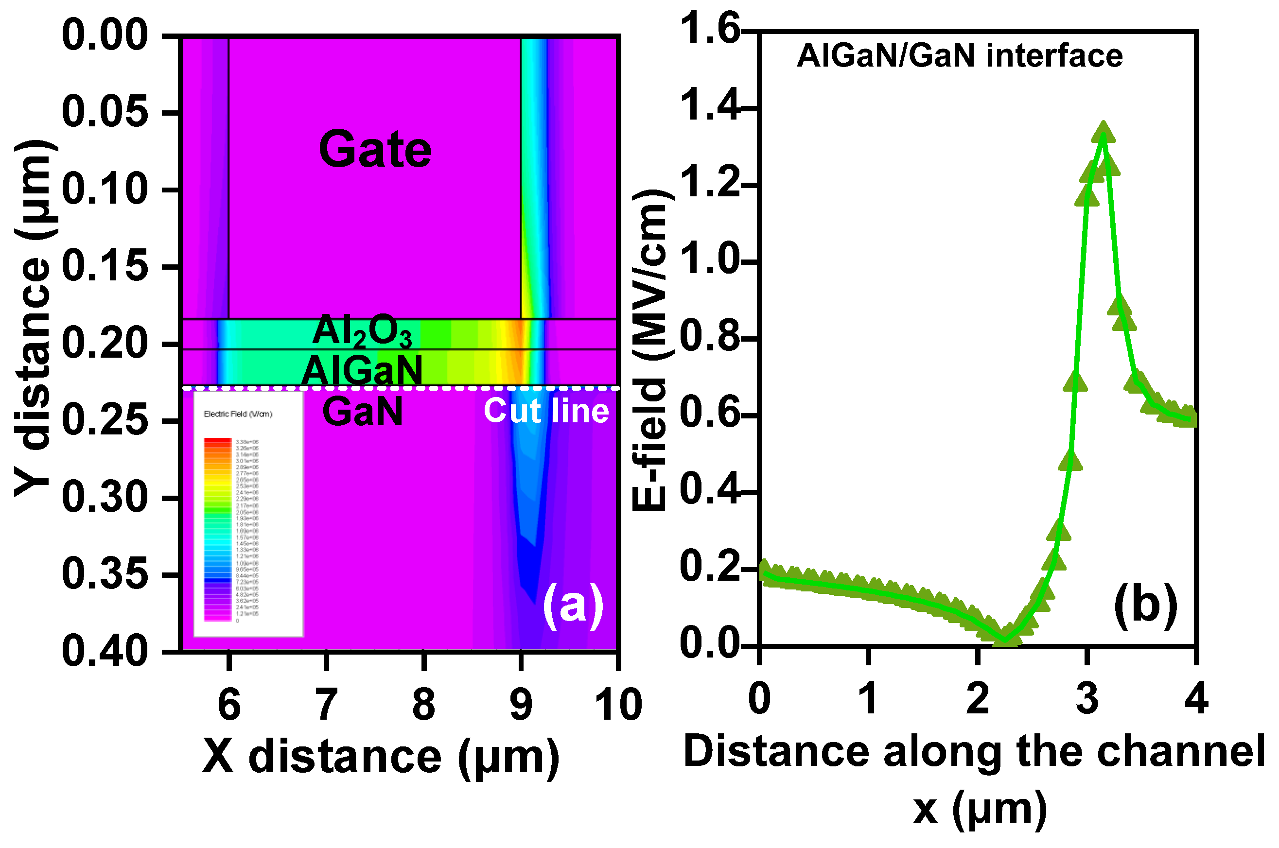
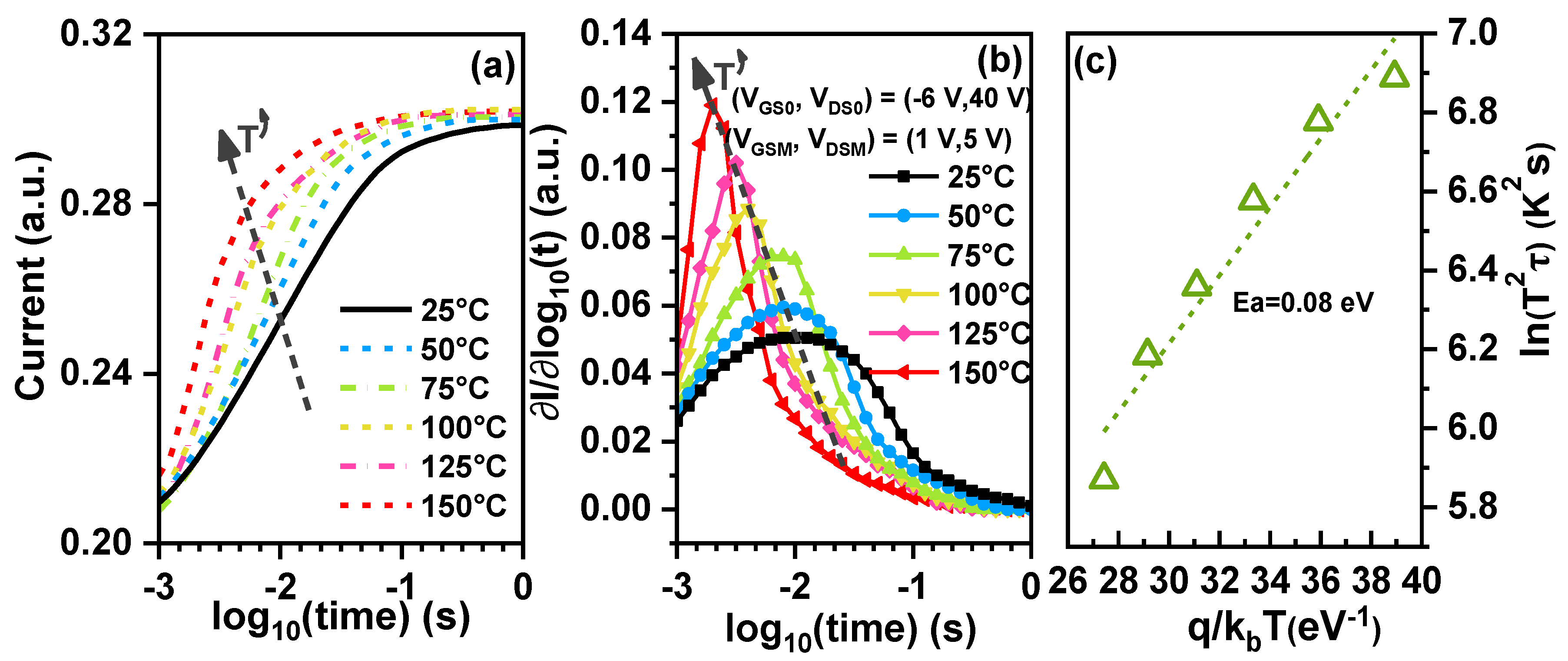
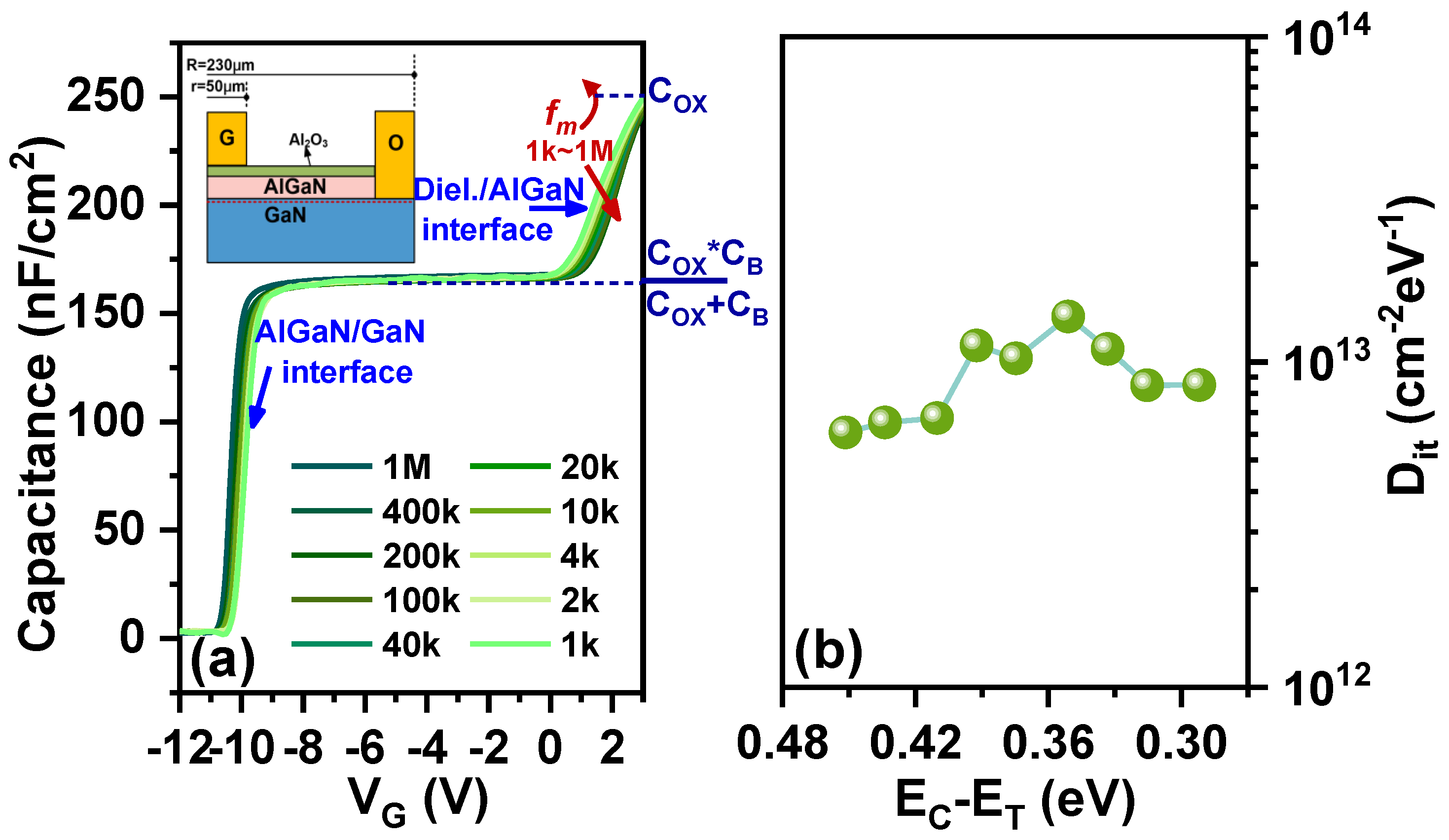
3. Current Collapse Results

Current collapse phenomena are tested by the pulse I-V method; two Agilent B1500A High-Resolution-Source Monitor Units (HRSMUs) provide gate and drain pulses; the pulse width ratio of the stress phase to the sampling phase is T s t r e s s / T o n = 130 ms/500 μ s. During the stress phase, the gate and drain voltage are defined as V G S , 0 and V D S , 0 , respectively. The devices are subjected to two stress conditions: off-state stress (with V G S , 0 = −8 V and V D S , 0 = 40 V) and semi-on-state stress (with V G S , 0 = −6 V and V D S , 0 = 40 V).
After the stress phase, the transient drain current I D is monitored at an on-state gate bias ( V G S , M ) of 0 V and a drain-source voltage ( V D S , M ) ranging from 1 V to 10 V. The on-resistance before the stress phase ( R O N , 0 ) and after the stress phase (dynamic on-resistance R O N , D ) is determined by dividing V D S , M by the transient on-state current observed at V G S , M = 0 V and V D S , M = 1 V. The R O N , D -to- R O N , 0 ratio represents the on-resistance degradation.
In Figure 4a, it is evident that the current collapse is more severe under semi-on-state stress than under off-state stress. The maximum I D decreases significantly, with a reduction of about 10% under semi-on-state stress and approximately 2% under off-state stress. In Figure 4b, the stress time increases from 100 ms to 1000 ms, while the sampling phase remains at 500 μ s. It has been observed that with increased stress time, the transient current I D decreases, indicating an increase in dynamic on-resistance [20,21]. Before 200 ms of stress, on-resistance degradation is similar for both conditions. After 200 ms, dynamic on-resistance increases more under semi-on-state stress than under off-state stress. At 1000 ms, the R O N , D -to- R O N , 0 ratio is 19 for semi-on-state stress and 10 for off-state stress.
Silvaco TCAD was used to model the device and simulate its electric field. To determine the high-density 2DEG channel, spontaneous and piezoelectric polarization models, the Shockley–Read–Hall (SRH) model [22], and Fermi–Dirac statistics were employed. The Albrecht model and the GaN velocity saturation model were used to characterize carrier behavior in low and high electric fields, respectively. Hot electron injection was modeled to assess the current under semi-on-state stress. The metal work function for the source and drain is 3.93 eV, while the work function for the gate is 5.05 eV. The GaN buffer is carbon-doped with a concentration of 5 × 10 16 cm 3 .
The electrical field profile of the device under semi-on-state stress ( V G S = −6 V and V D S = 40 V) is shown in Figure 5a, and the distribution along the AlGaN/GaN interface (or at the 2DEG channel) is shown in Figure 5b. The electric field is concentrated in the oxide layer and AlGaN-layer region beneath the gate, with the highest electric field occurring at the edge of the gate on the drain side. Along the cut line at the 2DEG channel, the maximum electric field peak is about 1.3 MV / cm .

4. Discussion

The temperature-dependent transient recovery current test investigates the location and distribution of trap levels responsible for R O N degradation under semi-on-state stress [23]. The test setup is shown in Figure 6a,b, the Agilent B1505A High-Current-Source Monitor Unit (HCSMU) and HPSMU provide the gate and drain pulses. Initially, a semi-on-state stress condition of ( V G S , 0 , V D S , 0 ) = (−6 V, 40 V) is applied to the device for 5 s to induce electron trapping. The transient recovery current is then monitored for 1 s under an on-state condition of ( V G S , M , V D S , M ) = (1 V, 5 V). A 1000 Ω resistor is connected to the device’s source electrode for this test. The test temperature is gradually raised from 25 °C to 150 °C, with a step of 25 °C. The temperature-dependent transient recovery current I D is calculated by detecting the real-time voltage difference across the resistor during device-switching.
The results are shown in Figure 7a. It has been found that at the starting point of 1 ms, the current density is not sensitive to temperature and remains at around 0.21. The saturation of the recovery current occurs earlier as the temperature increases, indicating that the device recovers faster at a higher temperature [24]. Figure 7b shows the extracted emission time constant (τe) spectra for the transient recovery currents of the device. The τe decreases with the temperature increase, from 11 ms to 1.9 ms, as the temperature rises from 25 °C to 150 °C. Figure 7c shows that the activation energy of traps is 0.08 eV below the conduction band. The fact that this activation energy is less than 0.1 eV indicates that the interface traps are the primary cause of R O N degradation [18,25].
Multi-frequency capacitance–voltage tests are performed on the MIS diode to determine the density of interface traps. The dielectric thickness is the same as that of MIS-HEMTs. The gate voltage is swept from −12 V to 3 V with a step of 50 mV. The AC small signal is 0.2 V, and the measurement frequency ( f m ) is varied from 1 kHz to 1 MHz. As the gate voltage increases, two slopes reflect different interface characteristics. At V G S = −11 V, electrons accumulate in the 2DEG channel. At this point, the frequency dispersion originates from the AlGaN/GaN interface. Subsequently, at V G S from −11 V to −9 V, the capacitance increases until it reaches a constant value. This constant value is equal to the series capacitance of the dielectric and the AlGaN barrier layer. When the gate voltage is increased to 0 V, the capacitance increases again as electrons are transferred to the dielectric/semiconductor interface. At this point, the interface trap states exhibit frequency-dependent characteristics.
Figure 8a shows that the voltage difference at the start of the second slope ( V O N ) corresponds to the interface traps responding at different frequencies [26,27]. V O N shifts positively with increasing frequency. The voltage dispersion ( Δ V O N ) observed at two measurement frequencies (f1 and f2) is attributed to the presence of interface traps within the energy range from E t r a p ( f 1 ) to E t r a p ( f 2 ) . The energy level of the detectable interface trap, E t r a p ( f m ) , as a function of the measurement frequency f m , can be expressed as
E t r a p ( f m ) = E C E T = k T l n ν t h σ n N C 2 π f m .
Here, k represents Boltzmann’s constant, T is the measurement temperature, N C = 2.7 × 10 18 cm 3 is the effective density of states in the conduction band of GaN, and σ n is the electron capture cross-section, assumed to be 1 × 10 14 cm 2 [28,29,30,31,32]. The thermal velocity of electrons, ν th , is 2 × 10 7 cm · s 1 .
The interface trap density at different frequencies, as shown in Figure 8b, ranges from 1.37 × 10 13 to 6.07 × 10 12 cm 2 eV 1 for E C E T = 0.29 eV to 0.45 eV , indicating that interface traps closer to the conduction band edge have a higher density. This observation is consistent with findings reported in other studies [28,33,34,35,36,37,38].
The following Table 1 compares the MIS diode with different insulators and surface treatments. Specifically, it is important to note that this paper investigates the degradation of the device under semi-on-state stress, attributed to hot-electron and self-heating effects. Therefore, it is necessary to consider the variation in substrate materials, as different substrates have different thermal conductivity. For example, sapphire ( K S a p p = 0.35 W/cm−K), Si ( K S i = 1.5 W/cm−K), SiC ( K S i C = 4.9 W/cm−K), and diamond ( K D i a = 20 W/cm−K) [39]. Therefore, the following table compares the interface traps for different insulator materials under the same substrate (Si).
According to the above test results, the current collapse phenomena under semi-on-state stress are more severe than under off-state stress due to hot electrons being injected and trapped in the bulk or at the interface, as shown in Figure 4a [40]. Furthermore, we found that R O N degradation is more pronounced in devices with larger access areas due to more interface traps [41].

5. Conclusions

This work investigates the current collapse in AlGaN/GaN MIS-HEMTs with 20 nm Al2O3 as their gate dielectric under off-state and semi-on-state stress. Traps cause on-resistance degradation under semi-on-state stress in the bulk and at the interface. The energy level and density of interface traps are determined using temperature-dependent transient recovery current tests and multi-frequency C-V tests, with an energy level of 0.08 eV and an interface trap density ranging from 1.37 × 10 13 to 6.07 × 10 12 cm 2 eV 1 for E C E T = 0.29 eV to 0.45 eV .

Author Contributions

Investigation, J.D.; Writing—original draft, Y.L.; Supervision, J.Z. and W.L.; Project administration, P.Z. and K.L.L. All authors have read and agreed to the published version of the manuscript.

Funding

This research was funded by the Suzhou Industrial Park High Quality Innovation Platform of Functional Molecular Materials and Devices (YZCXPT2023105) and the XJTLU Advanced Materials Research Center (AMRC).

Data Availability Statement

Data are contained within the article.

Conflicts of Interest

The authors declare no conflict of interest.

References

  1. Stradiotto, R.; Pobegen, G.; Ostermaier, C.; Waltl, M.; Grill, A.; Grasser, T. Characterization of Interface Defects With Distributed Activation Energies in GaN-Based MIS-HEMTs. IEEE Trans. Electron Devices 2017, 64, 1045–1052. [Google Scholar] [CrossRef]
  2. Hashizume, T.; Ootomo, S.; Hasegawa, H. Suppression of Current Collapse in Insulated Gate AlGaN/GaN Heterostructure Field-Effect Transistors Using Ultrathin Al2O3 Dielectric. Appl. Phys. Lett. 2003, 83, 2952–2954. [Google Scholar] [CrossRef]
  3. Wang, H.C.; Hsieh, T.E.; Lin, Y.C.; Luc, Q.H.; Liu, S.C.; Wu, C.H.; Dee, C.F.; Majlis, B.Y.; Chang, E.Y. AlGaN/GaN MIS-HEMTs With High Quality ALD-Al2O3 Gate Dielectric Using Water and Remote Oxygen Plasma As Oxidants. IEEE J. Electron Devices Soc. 2018, 6, 110–115. [Google Scholar] [CrossRef]
  4. Anand, M.J.; Ng, G.I.; Vicknesh, S.; Arulkumaran, S.; Ranjan, K. Reduction of Current Collapse in AlGaN/GaN MIS-HEMT with Bilayer SiN/Al2O3 Dielectric Gate Stack. Phys. Status Solidi C 2013, 10, 1421–1425. [Google Scholar] [CrossRef]
  5. Shen, L.; Zhang, D.; Cheng, X.; Zheng, L.; Xu, D.; Wang, Q.; Li, J.; Cao, D.; Yu, Y. Performance Improvement and Current Collapse Suppression of Al2O3/AlGaN/GaN HEMTs Achieved by Fluorinated Graphene Passivation. IEEE Electron Device Lett. 2017, 38, 596–599. [Google Scholar] [CrossRef]
  6. Filatova, E.O.; Konashuk, A.S. Interpretation of the Changing the Band Gap of Al2O3 Depending on Its Crystalline Form: Connection with Different Local Symmetries. J. Phys. Chem. C 2015, 119, 20755–20761. [Google Scholar] [CrossRef]
  7. Hashizume, T.; Nishiguchi, K.; Kaneki, S.; Kuzmik, J.; Yatabe, Z. State of the Art on Gate Insulation and Surface Passivation for GaN-Based Power HEMTs. Mater. Sci. Semicond. Process. 2018, 78, 85–95. [Google Scholar] [CrossRef]
  8. Lossy, R.; Gargouri, H.; Arens, M.; Würfl, J. Gallium Nitride MIS-HEMT Using Atomic Layer Deposited Al2O3 as Gate Dielectric. J. Vac. Sci. Technol. A 2013, 31, 01A140. [Google Scholar] [CrossRef]
  9. Low, R.S.; Chen, C.-Y.; Su, M.-H.; Lin, H.-T.; Chang, C.-Y. GaN-Based MIS-HEMTs with Al2O3 Dielectric Deposited by Low-Cost and Environmental-Friendly Mist-CVD Technique. Appl. Phys. Express 2021, 14, 031004. [Google Scholar] [CrossRef]
  10. Asubar, J.T.; Kawabata, S.; Tokuda, H.; Yamamoto, A.; Kuzuhara, M. Enhancement-Mode AlGaN/GaN MIS-HEMTs With High VTH and High IDmax Using Recessed-Structure With Regrown AlGaN Barrier. IEEE Electron Device Lett. 2020, 41, 693–696. [Google Scholar] [CrossRef]
  11. Hatano, M.; Taniguchi, Y.; Kodama, S.; Tokuda, H.; Kuzuhara, M. Reduced Gate Leakage and High Thermal Stability of AlGaN/GaN MIS-HEMTs Using ZrO2/Al2O3 Gate Dielectric Stack. Appl. Phys. Express 2014, 7, 044101. [Google Scholar] [CrossRef]
  12. Yao, Y.; Huang, S.; Jiang, Q.; Wang, X.; Bi, L.; Shi, W.; Guo, F.; Luan, T.; Fan, J.; Yin, H.; et al. Identification of Semi-ON-State Current Collapse in AlGaN/GaN HEMTs by Drain Current Deep Level Transient Spectroscopy. IEEE Electron Device Lett. 2022, 43, 200–203. [Google Scholar] [CrossRef]
  13. Modolo, N.; De Santi, C.; Minetto, A.; Sayadi, L.; Sicre, S.; Prechtl, G.; Meneghesso, G.; Zanoni, E.; Meneghini, M. A Physics-Based Approach to Model Hot-Electron Trapping Kinetics in p-GaN HEMTs. IEEE Electron Device Lett. 2021, 42, 673–676. [Google Scholar] [CrossRef]
  14. Dutta Gupta, S.; Joshi, V.; Chaudhuri, R.R.; Shrivastava, M. Unique Role of Hot-Electron Induced Self-Heating in Determining Gate-Stack Dependent Dynamic RON of AlGaN/GaN HEMTs Under Semi-On State. IEEE Trans. Electron Devices 2022, 69, 6934–6939. [Google Scholar] [CrossRef]
  15. Fabris, E.; Meneghini, M.; De Santi, C.; Borga, M.; Kinoshita, Y.; Tanaka, K.; Ishida, H.; Ueda, T.; Meneghesso, G.; Zanoni, E. Hot-Electron Trapping and Hole-Induced Detrapping in GaN-Based GITs and HD-GITs. IEEE Trans. Electron Devices 2019, 66, 337–342. [Google Scholar] [CrossRef]
  16. Chaudhuri, R.R.; Joshi, V.; Gupta, S.D.; Shrivastava, M. On the Channel Hot-Electron’s Interaction With C-Doped GaN Buffer and Resultant Gate Degradation in AlGaN/GaN HEMTs. IEEE Trans. Electron Devices 2021, 68, 4869–4876. [Google Scholar] [CrossRef]
  17. Meneghini, M.; Ronchi, N.; Stocco, A.; Meneghesso, G.; Mishra, U.K.; Pei, Y.; Zanoni, E. Investigation of Trapping and Hot-Electron Effects in GaN HEMTs by Means of a Combined Electrooptical Method. IEEE Trans. Electron Devices 2011, 58, 2996–3003. [Google Scholar] [CrossRef]
  18. Pan, S.; Feng, S.; Zheng, X.; He, X.; Li, X.; Bai, K. Effects of Temperature and Bias Voltage on Electron Transport Properties in GaN High-Electron-Mobility Transistors. IEEE Trans. Device Mater. Reliab. 2021, 21, 494–499. [Google Scholar] [CrossRef]
  19. Zhang, Y.; Sun, Z.; Wang, W.; Liang, Y.; Cui, M.; Zhao, Y.; Wen, H.; Liu, W. Low-Resistance Ni/Ag Contacts on GaN-Based p-Channel Heterojunction Field-Effect Transistor. IEEE Trans. Electron Devices 2023, 70, 31–35. [Google Scholar] [CrossRef]
  20. Bisi, D.; Meneghini, M.; Marino, F.A.; Marcon, D.; Stoffels, S.; Van Hove, M.; Decoutere, S.; Meneghesso, G.; Zanoni, E. Kinetics of Buffer-Related RON Increase in GaN-on-Silicon MIS-HEMTs. IEEE Electron Device Lett. 2014, 35, 1004–1006. [Google Scholar] [CrossRef]
  21. Zhou, X.; Tan, X.; Lv, Y.; Wang, Y.; Song, X.; Gu, G.; Xu, P.; Guo, H.; Feng, Z.; Cai, S. Dynamic Characteristics of AlGaN/GaN Fin-MISHEMTs With Al2O3 Dielectric. IEEE Trans. Electron Devices 2018, 65, 928–935. [Google Scholar] [CrossRef]
  22. Hariz, A.J.; Rathmell, J.G.; Varadan, V.K.; Parker, A.E. Circuit Implementation of a Theoretical Model of Trap Centres in GaAs and GaN Devices. In Proceedings of the Microelectronics: Design, Technology, and Packaging III, Canberra, ACT, Australia, 4–7 December 2007. [Google Scholar] [CrossRef]
  23. Wang, M.; Yan, D.; Zhang, C.; Xie, B.; Wen, C.P.; Wang, J.; Hao, Y.; Wu, W.; Shen, B. Investigation of Surface- and Buffer-Induced Current Collapse in GaN High-Electron Mobility Transistors Using a Soft Switched Pulsed I-V Measurement. IEEE Electron Device Lett. 2014, 35, 1094–1096. [Google Scholar] [CrossRef]
  24. Zhang, C.; Wang, M.; Xie, B.; Wen, C.P.; Wang, J.; Hao, Y.; Wu, W.; Chen, K.J.; Shen, B. Temperature Dependence of the Surface- and Buffer-Induced Current Collapse in GaN High-Electron Mobility Transistors on Si Substrate. IEEE Trans. Electron Devices 2015, 62, 2475–2480. [Google Scholar] [CrossRef]
  25. Zheng, X.; Feng, S.; Zhang, Y.; He, X.; Wang, Y. A New Differential Amplitude Spectrum for Analyzing the Trapping Effect in GaN HEMTs Based on the Drain Current Transient. IEEE Trans. Electron Devices 2017, 64, 1498–1504. [Google Scholar] [CrossRef]
  26. Wu, J. Nitride Based Metal Insulator Semiconductor Heterostructure Material and Device Design and Characterization. Ph.D. Dissertation, University of California, Los Angeles, CA, USA, 2014. Available online: https://escholarship.org/uc/item/3zr5s480 (accessed on 18 September 2024).
  27. Shu, Y.; Shenghou, L.; Yunyou, L.; Cheng, L.; Chen, K.J. AC Capacitance Techniques for Interface Trap Analysis in GaN-Based Buried-Channel MIS-HEMTs. IEEE Trans. Electron Devices 2015, 62, 1870–1878. [Google Scholar] [CrossRef]
  28. Cai, Y.; Liu, W.; Cui, M.; Sun, R.; Liang, Y.C.; Wen, H.; Yang, L.; Supardan, S.N.; Mitrovic, I.Z.; Taylor, S.; et al. Effect of surface treatment on electrical properties of GaN metal–insulator–semiconductor devices with Al2O3 gate dielectric. Jpn. J. Appl. Phys. 2020, 59, 041001. [Google Scholar] [CrossRef]
  29. Matys, M.; Stoklas, R.; Kuzmik, J.; Adamowicz, B.; Yatabe, Z.; Hashizume, T. Characterization of capture cross sections of interface states in dielectric/III-nitride heterojunction structures. J. Appl. Phys. 2016, 119, 205304. [Google Scholar] [CrossRef]
  30. Rocha, P.F.P.P. Optimization of Dielectric/GaN Interface for MIS Gate Power Devices. Ph.D. Thesis, Université Grenoble Alpes, Grenoble, France, 2024. Available online: https://theses.hal.science/tel-04496081 (accessed on 18 September 2024).
  31. Liu, S.; Yang, S.; Tang, Z.; Jiang, Q.; Liu, C.; Wang, M.; Shen, B.; Chen, K.J. Interface/border trap characterization of Al2O3/AlN/GaN metal-oxide-semiconductor structures with an AlN interfacial layer. Appl. Phys. Lett. 2015, 106, 051605. [Google Scholar] [CrossRef]
  32. Huang, S.; Jiang, Q.; Yang, S.; Tang, Z.; Chen, K.J. Mechanism of PEALD-Grown AlN Passivation for AlGaN/GaN HEMTs: Compensation of Interface Traps by Polarization Charges. IEEE Electron Device Lett. 2013, 34, 193–195. [Google Scholar] [CrossRef]
  33. Yang, S.; Liu, S.; Liu, C.; Lu, Y.; Chen, K.J. Nitridation interfacial-layer technology for enhanced stability in GaN-based power devices. In Proceedings of the 2015 IEEE International Symposium on Radio-Frequency Integration Technology (RFIT), Sendai, Japan, 26–28 August 2015. [Google Scholar] [CrossRef]
  34. Cai, Y.; Wang, Y.; Liang, Y.; Zhang, Y.; Liu, W.; Wen, H.; Mitrovic, I.Z.; Zhao, C. Effect of High-k Passivation Layer on High Voltage Properties of GaN Metal-Insulator-Semiconductor Devices. IEEE Access 2020, 8, 95642–95649. [Google Scholar] [CrossRef]
  35. Zhu, J.J.; Ma, X.H.; Xie, Y.; Hou, B.; Chen, W.W.; Zhang, J.C.; Hao, Y. Improved Interface and Transport Properties of AlGaN/GaN MIS-HEMTs with PEALD-Grown AlN Gate Dielectric. IEEE Trans. Electron Devices 2015, 62, 512–518. [Google Scholar] [CrossRef]
  36. Mehari, S.; Gavrilov, A.; Eizenberg, M.; Ritter, D. Density of Traps at the Insulator/III-N Interface of GaN Heterostructure Field-Effect Transistors Obtained by Gated Hall Measurements. IEEE Electron Device Lett. 2015, 36, 893–895. [Google Scholar] [CrossRef]
  37. Sun, H.; Wang, M.; Yin, R.; Chen, J.; Xue, S.; Luo, J.; Hao, Y.; Chen, D. Investigation of the Trap States and VTH Instability in LPCVD Si3N4/AlGaN/GaN MIS-HEMTs with an In-Situ Si3N4 Interfacial Layer. IEEE Trans. Electron Devices 2019, 66, 3290–3295. [Google Scholar] [CrossRef]
  38. Lin, Y.C.; Huang, Y.X.; Huang, G.N.; Wu, C.H.; Yao, J.N.; Chu, C.M.; Chang, S.; Hsu, C.C.; Lee, J.H.; Kakushima, K.; et al. Enhancement-Mode GaN MIS-HEMTs with LaHfOx Gate Insulator for Power Application. IEEE Electron Device Lett. 2017, 38, 1101–1104. [Google Scholar] [CrossRef]
  39. Ranjan, K.; Arulkumaran, S.; Ng, G.I.; Sandupatla, A. Low interface trap density in AlGaN/GaN Metal-Insulator-Semiconductor High-Electron-Mobility Transistors on CVD-Diamond. In Proceedings of the 2020 4th IEEE Electron Devices Technology & Manufacturing Conference (EDTM), Penang, Malaysia, 6–21 April 2020. [Google Scholar] [CrossRef]
  40. Meneghini, M.; Rossetto, I.; Bisi, D.; Stocco, A.; Chini, A.; Pantellini, A.; Lanzieri, C.; Nanni, A.; Meneghesso, G.; Zanoni, E. Buffer Traps in Fe-Doped AlGaN/GaN HEMTs: Investigation of the Physical Properties Based on Pulsed and Transient Measurements. IEEE Trans. Electron Devices 2014, 61, 4070–4077. [Google Scholar] [CrossRef]
  41. Liang, Y.; Zhang, Y.; He, X.; Zhao, Y.; Cui, M.; Wen, H.; Liu, W. Study of Drain-current Collapse in AlGaN/GaN MIS-HEMTs with Different Gate Lengths. In Proceedings of the 2022 IEEE 16th International Conference on Solid-State & Integrated Circuit Technology (ICSICT), Nanjing, China, 25–28 October 2022. [Google Scholar] [CrossRef]
Figure 1. (a) The simplified schematic structure of AlGaN/GaN MIS-HEMTs with a 20 nm ALD-Al2O3 as gate dielectric and passivation. (b) The fabrication process of the device.
Nanomaterials 14 01529 g001
Figure 2. (a) Surface roughness after ICP etching. (b) Contact resistance was obtained using the TLM method.
Nanomaterials 14 01529 g002
Figure 3. (a) Transfer characteristics ( I D - V G S ) and (b) output characteristics ( I D - V D S ) of the devices. (c) Off-state breakdown test results with a floating substrate.
Nanomaterials 14 01529 g003
Figure 4. (a) Current collapse results are shown for off-state stress (green dotted line), semi-on-state stress (red dotted line), and no stress (black dotted line). (b) Changes in the R R O N , D / R O N , 0 ratio with increasing stress time.
Nanomaterials 14 01529 g004
Figure 5. (a) Electrical field profile of AlGaN/GaN MIS-HEMT under semi-on-state stress. (b) Electrical field distribution along the 2DEG channel.
Nanomaterials 14 01529 g005
Figure 6. (a) Schematic setup for transient measurement. (b) The semi-on-state stress at ( V G S , 0 , V D S , 0 ) = (−6 V, 40 V) is applied to the samples for 5 s. Then, after the stress period, the transient current is obtained by measuring the voltage drop across the resistive load during the on-state ( V G S , M , V D S , M ) = (1 V, 5 V) for 1 s.
Nanomaterials 14 01529 g006
Figure 7. (a) The temperature-dependent transient recovery current results after semi-on-state stress. (b) Emission time constant spectra extracted from the temperature-dependent transient recovery current results. (c) Arrhenius plots calculate the activation energy of AlGaN/GaN MIS-HEMTs with Al2O3 as dielectric under semi-on-state stress.
Nanomaterials 14 01529 g007
Figure 8. (a) Multi-frequency C-V characteristics of AlGaN/GaN MIS diode. (b) D i t - E T mapping in the MIS diode. Measurement frequency f m varies from 1 kHz to 1 MHz.
Nanomaterials 14 01529 g008
Table 1. Comparison of interface trap density and energy level of different insulators and surface treatments on Si substrate.
InsulatorSurface TreatmentTest MethodInterface Density (eV−1cm−2)Energy Level (eV)
Al2O3 [28]O2 plasmaMulti-frequency capacitance–voltage9.1 × 10 12 ~4.8 × 10 12 0.28 to 0.47
Al2O3 [28]OctadecanethiolMulti-frequency capacitance–voltage6.1 × 10 12 ~3 × 10 12 0.28 to 0.47
Al2O3 [33]N2 plasmaMulti-frequency capacitance–voltage6 × 10 12 ~6 × 10 11 0.24 to 0.78
Al2O3 (This work)HCl solutionMulti-frequency capacitance–voltage1.37 × 10 13 ~6.07 × 10 12 0.29 to 0.45
ZrO2 [34]HCl solutionMulti-frequency capacitance–voltage4.7 × 10 13 ~9.4 × 10 12 0.28 to 0.47
AlN [35]In situ low-damage plasmaC-V hysteresis2.0 × 10 13 No mention
SiNx [36]HF: H2O solutionGated Hall method2.3 × 10 13 ~4 × 10 12 1.2 to 2.3
S3N4 [37]HCl solutionHigh-frequency capacitance–voltage1.4 × 10 12 ~2.8 × 10 11 0.53 to 0.71
LaHfOx [38]Rapid thermal annealing at the gate recess regionC-V hysteresis7.5 × 10 11 No mention
Disclaimer/Publisher’s Note: The statements, opinions and data contained in all publications are solely those of the individual author(s) and contributor(s) and not of MDPI and/or the editor(s). MDPI and/or the editor(s) disclaim responsibility for any injury to people or property resulting from any ideas, methods, instructions or products referred to in the content.

