Article

Optimization of Substrate Sizes for In Situ Stress Measurement in Electrodeposits Relying on Nonlinear Effects

1
School of Mechanical Engineering, Ningxia University, Yinchuan 750021, China
2
State Key Laboratory of Precision Manufacturing for Extreme Service Performance, College of Mechanical and Electrical Engineering, Central South University, Changsha 410083, China
3
Zhuhai UM Science & Technology Research Institute, Zhuhai 519085, China
*
Author to whom correspondence should be addressed.
Coatings 2023, 13(12), 2031; https://doi.org/10.3390/coatings13122031
Submission received: 2 November 2023 / Revised: 22 November 2023 / Accepted: 29 November 2023 / Published: 30 November 2023

Abstract

:
In situ stress measurements have been widely used in various deposition processes for stress detection. The substrate size can affect the uniformity of curvature across the entire surface, which is a major cause of incorrect stress measurements. However, because of the inherent concept of measurement theory and the complexities of the influence of substrate size on measurement accuracy, the underlying nonlinear effects of the rectangular substrate are still not fully understood. We discovered that increasing the substrate size caused an increase in nonlinear effect (nonuniform distribution of curvature radii and stresses in the x and y directions) and surface defects on the rectangular substrate using in situ stress measurement. Furthermore, the bending stiffness of the substrate, which was influenced by the substrate size, was established to illustrate the effect of substrate size on the nonlinear effect. The total stress of the deposit was concentrated at the edge in both the x and y directions, and the deposit at the edge was prone to delamination and cracking. When the substrate size was reduced, the deposit surface did not show obvious defects, and the stress errors in the x and y directions were only 2.34% and 2.54%, respectively. These findings will be beneficial to improve the accuracy of in situ stress measurement and further understand the causes of nonlinear effects.

1. Introduction

In situ stress measurement is emerging as a powerful tool for understanding the relationship between stress evolution and the film growth process [1,2]. The basic concept of in situ stress measurement is that the curvature of a deposit-substrate system can be directly converted into stress using Stoney’s formula σ d ¯ = E s * h s 2 6 h d   k [3], and the stress changes can be obtained by real-time detection of the corresponding curvature during the deposition process. In Stoney’s formula, σ d ¯ is the average in-plane stress, k is the measured curvature, E s * = E s ( 1     v s ) is the biaxial elastic modulus, h s is the substrate thickness, and h d is the deposit thickness. Therefore, the measurement accuracy of curvature is the key to determining stress measurement accuracy. In this regard, many efforts have been made to promote the accuracy of curvature measurements, including enhanced detection capabilities and improved measurement sensitivity. For example, diversified sensors are employed to enhance the detection capabilities, such as a multibeam optical stress sensor [4], Shack–Hartmann sensor [5,6], and quadri-wave lateral shearing interferometry sensor [7]; to improve the measurement sensitivity of the substrate deformation, it is shown that using low elastic modulus substrate materials (quartz glass and polymethyl methacrylate) or reducing the substrate thickness is effective, the available thickness of deposit can be reduced to about 0.1 mm [7,8]. However, beyond these attempts, an intrinsic problem is that nonlinear effects (i.e., nonuniform curvature in different directions) are induced by large deformation of the substrate, leading to large errors in stress measurements [9,10].
According to the Stoney theory of in situ stress measurement, the nonlinear effect is directly related to the assumption that substrate deformation is consistent [10,11]. The nonlinear effect is strongly dependent on the shape and size of the substrate [8,12,13], which has received a lot of attention in this regard. For a circular substrate, Finot et al. have studied the evolution of the curvature with the substrate size, which depends on the value of A ( A = σ d ¯ h d D s 2 h s 3 , where D s is the diameter of the circular substrate). With the increase in A, the deformation of the substrate-deposition system increases continuously, and the curvature changes from uniform spherical to nonuniform cylinder through an elliptical stage, leading to an obvious nonlinear effect. Furthermore, for in situ stress measurements in electrodeposition, the substrate is typically rectangular, and previous work has suggested that the corresponding nonlinear effect of such substrates is controlled by size factors such as length and width [9,13]. Guyot and Mezin have demonstrated that when the length/width ratio is greater than 65/8, the relative change in curvatures in the x and y directions is less than 5% [13]. Therefore, in the in situ stress measurement experiment, a substrate with an appropriate length/width ratio should be chosen, which has always been neglected in previous studies. We have noticed that substrates with various length/width ratios are used for in situ stress measurements in previous work, such as 60/3 [14,15], 50/18 [16], and 60/15 [6]. It is obvious that the ratios of the last two sizes are smaller than the comparison value (65/8), thus making a large measurement error. Hence, it is still unclear how substrate sizes influence nonlinear effects.
In this work, we observed the evolution of the curvature and stress of the Ni electrodeposition using in situ stress measurement and analyzed the relationship between the substrate size and the nonlinear effect. Furthermore, the equivalent reference temperature (ERT) method has been proposed to simulate the value and distribution of stress in the thin films, which utilizes temperature loads caused by differences in temperature and thermal expansion coefficients between the substrate and the thin film to simulate thermal stress [17,18,19,20]. Here, we also use the ERT method to supplement the details that the experimental characterizations cannot acquire. We revealed the effect of substrate size on the nonlinear effect, the stress distribution, and the causes of nonlinear effects and surface defects in the deposit. Our study provides valuable insights for understanding the mechanism of surface defects on rectangular substrates and improving measurement accuracy.

2. Materials and Methods

2.1. The Equivalent Reference Temperature Method

The essence of the ERT method is to use temperature loading to model the internal stress in the film [17,20]. According to crystallographic theory, the internal stress of the electrodeposited layer can be simplified as lattice expansion (compressive stress) or contraction (tensile stress), and such lattice change can also be induced by thermal stimulation [20]. Therefore, the internal stress of the electrodeposited nickel layer can be simulated by thermal stress caused by the temperature load. Here, the stress simulation by the ERT method was carried out using the static module in ANSYS 19.2. In accordance with the basic steps of finite element simulation, the simulation process is as follows:
(1) Establishment of the geometric model. Figure 1a shows a three-dimensional solid model of the electrodeposited Ni layer. The model comprised a quartz glass substrate (blue) and a nickel deposit (orange). During electrodeposition, the substrate was partially immersed in the electrolyte; therefore, the size of the deposit was smaller than that of the substrate. In the simulation, the materials of substrate and deposit were assumed to be isotropic and homogeneous, and their mechanical properties are listed in Table 1.
To study the influence of substrate size on the deposition stress in different directions, we designed three groups of parameters. The detailed dimension parameters are listed in Table 2.
(2) Mesh division. Automatic meshing with ANSYS software (v19.2) is difficult because the substrate’s and deposit’s thickness differ by an order of magnitude. Multizone and Mapped Mesh Types were used for hexahedral meshing to improve the simulation accuracy of the stress distribution of the substrate and deposit. The element sizes in the thickness direction of the substrate and the deposit were 50 μm and 2 μm, respectively. The figure after meshing of the model is shown in Figure 1b.
(3) Constraints and Loads. The substrate was clamped in the experiment on a single side to form a cantilever beam. Therefore, in the simulation, a fixed displacement constraint was imposed on the edge of the substrate, which was not immersed in the electrolyte. On the other edge of the substrate, the deformation of the quartz glass and nickel layer was the same, and the contact type between the substrate and the deposit was bonded to avoid gaps or slippage.
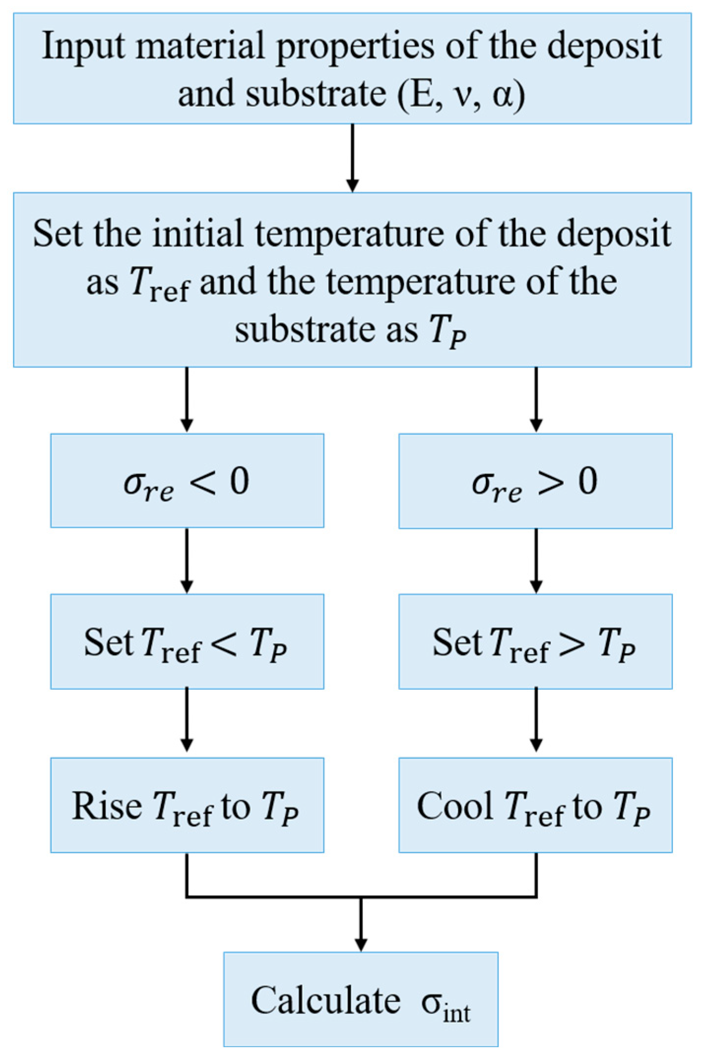
The temperature load was generated by the temperature difference between the equivalent reference temperature ( T r e f ) and the actual process temperature ( T p ). The T r e f was the initial temperature of the nickel layer in the model. The T p was the final temperature of the nickel layer. If the experimental stress ( σ r e ) was tensile, the cooling process ( T r e f > T p ) would be used to simulate the generation of the intrinsic stress. Conversely, if the experimental stress was compressive, the heating process ( T r e f < T p ) would be used. In this work, the T p was equal to the ambient temperature, assumed to be 295.15 K. The stress of the electrodeposited nickel layer was mostly tensile, so the T r e f was set greater than T p . In addition, the temperature of the substrate was set as T p and kept constant. Then, the formula equation for the stress of the nickel layer can be expressed as
σ i n t = α d T p T r e f 1     ν d E d + 1     ν s E s h d h s
(4) Therefore, the stress of the nickel layer ( σ i n t ) was calculated. The workflow of simulation by the ERT method is shown in Figure 2.

2.2. The Curvature Radius of a Substrate-Deposit System in the Simulation

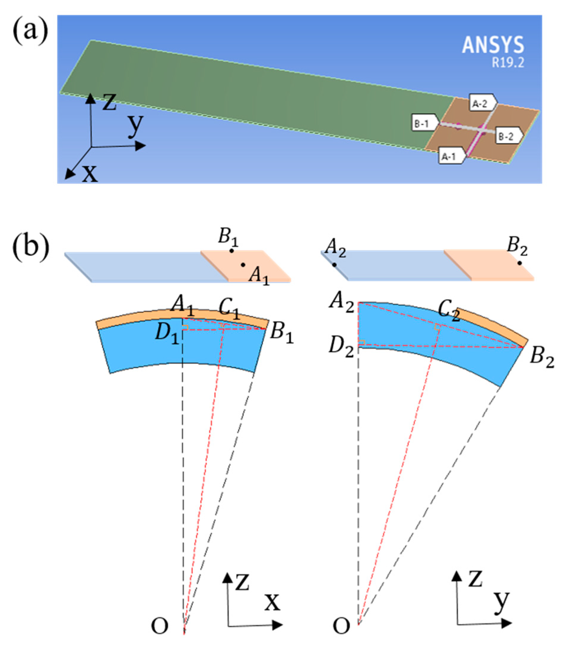
To obtain the curvature radius and stress of the deposit in different directions, extraction paths were set within the deposit during data post-processing, as shown in Figure 3a. Lines A-1 to A-2 and B-1 to B-2 represent the x and y directions, respectively. We calculated the radius of curvature after deformation, referring to the method reported by Hsi-Chao Chen et al. [19], as shown in Figure 3b. For the x-direction, we extracted the displacements of points A 1 and B 1 in the x- and z-directions in the xoz plane; A 1 D 1 ¯ is the displacement difference at the point A 1 in the z-direction before and after deformation and B 1 D 1 ¯ is the displacement difference of point B 1 in the x-direction before and after deformation. The same process is also applied for the y-direction, and the marker is identified by the subscript with 2, such as A2, B2, C2, and D2. Two similar right triangles ( O A i C i and A B i D i ,   i = 1   o r   2 ) were constructed, and the radius of curvature was obtained as
B i A i ¯ O A i ¯ = A i D i ¯ A i C i ¯ = B i D i ¯ O C i ¯
O A i ¯ = B i A i ¯ A i C i ¯ A i D i ¯
where B i A i ¯ = ( A i D i ¯ ) 2 + ( B i D i ¯ ) 2 and A i C i ¯ = B i A i ¯ / 2 . The O A i ¯ lines are the curvature radius of the deposit. The curvature radius O A i ¯ after deformation can be calculated according to Equation (3), and the corresponding stress value can be obtained based on the Stoney formula.

2.3. In Situ Stress Measurement of Ni Electrodeposition

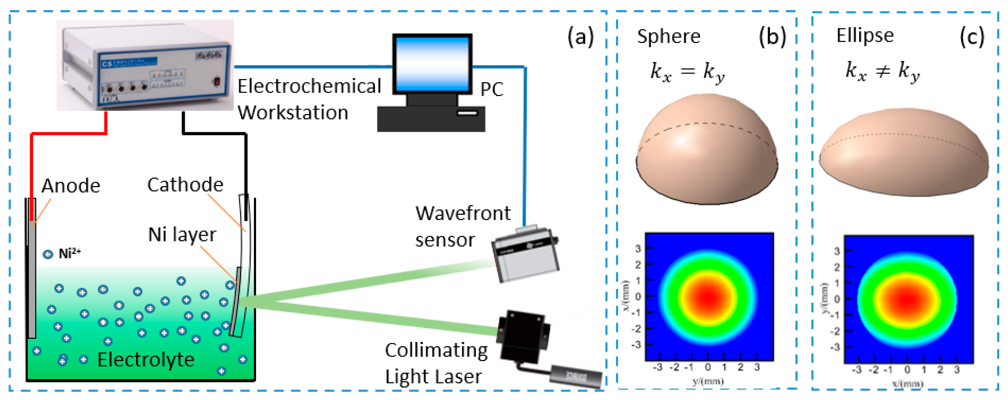
We used a self-developed electrodeposition system for stress measurement with high accuracy, consisting of a Quadri-wave Lateral Shear Wavefront Sensor (SID4-HR, Phasics@ Corp., Saint-Aubin, France), Collimating Light Source (R-cube, Phasics@ Corp., Saint-Aubin, France), Electrochemical Workstation (CHI600E, Shanghai Chinstruments@ Corp., Shanghai, China), and a Haring Cell. A schematic of the measurement apparatus is shown in Figure 4a. The laser (λ = 532 nm) sequentially passed through the transparent electrodeposition cell, electrolyte, and substrate. The reflection was generated in the interface between the deposit and the substrate, and the reflected light was detected by the wavefront sensor. The curvature of the substrate was measured in situ by the principle of transverse shearing interference [7]. The internal stress of the deposit can be calculated from the curvature of the substrate. The wavefront sensor can also obtain the phase map of the wavefront, which can directly reflect the surface topography of the sample. When the deformation of the sample surface is a spherical shape, the resulting wavefront phase map is circular, as shown in Figure 4b; when the deformation of the sample surface is an ellipsoid, the map shows an ellipse shape, as shown in Figure 4c. Therefore, the surface deformation of the sample can be directly reflected by the wavefront phase map, indicating whether there is a nonlinear effect in the measurement process or not.
A 30 nm thick Au film as a conductive layer was coated on the surface of the substrate using a high-vacuum sputter coater (EMSCD 500, Leica@ Corp, Frankfurt, Germany) for 240 s. Because the conductive layer was very thin, the influence of the conductive layer was ignored in simulations [17,21]. The size of the deposits can be controlled by adjusting the height of the electrolyte (the major ingredients of the electrolyte can be seen in Table S1). An electrochemical workstation (CHI600E, CH Instruments, Bee Cave, TX, USA) was used as the power source to output direct current by chronopotentiometry. The deposition current density was 1 A/dm2, and the deposit was electrodeposited for 30 min at a sampling interval of 30 s.

3. Results and Discussion

3.1. Effect of Substrate Width on the Curvature Radius and the Internal Stress of Nickel Deposits in Experiments

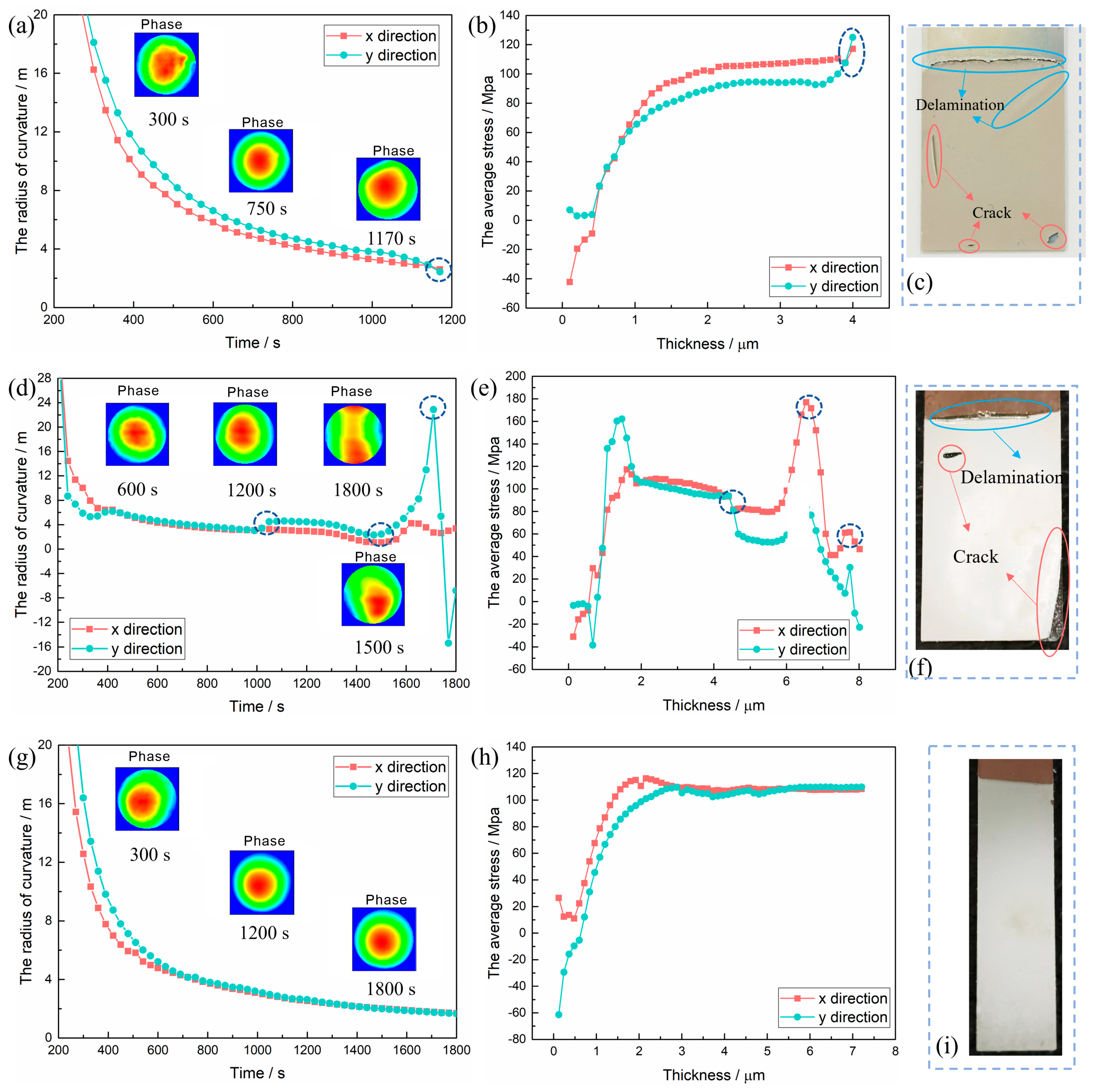
A series of in situ stress measurements have been carried out to observe the evolution of the curvature radius and stress under different substrate widths. The thickness of corresponding deposits is less than 0.8 μm for the different substrate widths, as shown in Figure 5a–c, and the radii of curvature in the x and y directions show large differences within the first 200 s. Because the initial growth stage of electrodeposited nickel gradually consists of island growth, contact, merger, and continuous deposit formation [22,23]; the stress state changes continuously at different growth stages, and the stress in different directions also shows significant differences. Furthermore, the slight deformation of the substrate at the initial stage makes the radius of curvature difficult to measure. When the deposit time was between 200 and 1000 s (the thickness of the corresponding deposit was 0.8 to 4 μm), the difference gradually decreased and approached a constant value. Therefore, this work mainly focuses on the electrodeposition process after 200 s.
When the substrate width is 15 mm, as shown in Figure 6a, the radii of curvature in the x- and y-directions are different. There is also a difference between the stresses in the x- and y-directions, about 20 MPa (Figure 6b). At the same time, the phase map is elliptical (see inset in Figure 6a), which intuitively indicates that the surface curvatures are different in the x and y directions. The curvature radius and the stress inhomogeneity indicate that the deformation of the substrate-deposit system is affected by nonlinear effects. A sudden change occurs after 1170 s (dotted-line circle in Figure 6a,b), and the electrodeposition process stops. The reason is that the delamination of the upper edge causes the deposit to separate from the conductive layer so that the electrodeposition is interrupted and stopped. As shown in Figure 6c, cracks and delamination appear in the deposit, mainly at the upper edge.
When the substrate width is 10 mm, the curvature radii and stresses in the x- and y-directions exhibit some sudden changes (the dotted-line circle), as shown in Figure 6d,e. This is due to severe delamination and cracks on the surface of the deposit (see Figure 6f). The phase map is also elliptical (see inset in Figure 6d), which intuitively indicates that the surface curvatures are different in the x and y directions. The deformation of the substrate-deposit system is still affected by the nonlinear effect. With the deposition time increase, the deposited layer’s surface defects gradually increased, and the deformation difference in different directions gradually became significant. The phase map approached towards a cylindrical shape under the influence of the surface defects.
Interestingly, when the substrate width is reduced to 5 mm, as shown in Figure 6g,h, one can see that the values of the curvature radii and stresses in the x- and y-directions are close to the same. Moreover, there are no obvious defects on the surface of the deposit (Figure 6i), and the phase map is close to a circle (see inset in Figure 6g), indicating that the surface deformation of the deposit in different directions is consistent and the surface curvature is uniform.
The above experimental results address that the nonlinear effect and surface defects existing on rectangular substrates can be reduced by lowering the width of the substrate. When the substrate width is 5 mm, there are no nonlinear effects and surface defects.

3.2. Effect of Substrate Width on the Curvature Radius of the Deposit in the Simulation

To thoroughly figure out the effect of substrate width on nonlinear effect, the simulation method of ERT has been used to explore the changes in the curvature radius of deposits along with the diversified substrate widths. After applying the equivalent reference temperature, the deformations of the substrate-deposit system in the x- and y-directions are shown in Figure S1. The radius of curvature after deformation is calculated by Equation (3), as shown in Figure 7a,c. With the increase in the substrate width, the radius of curvature in the x-direction increases while that in the y-direction decreases; the difference between the radii of curvature in the x- and y-directions increases with the substrate width (Figure 7a). The error of the curvature radii in the x- and y-directions with a substrate width of 5 mm is only 3.8%, while that with a substrate width of 20 mm is as high as 67.5%. Further, we compare the average stress ( σ s t ) converted from the curvature radius by Stoney’s formula and the average stress ( σ s i ) calculated by the ERT simulation. As shown in Figure 7b, the average stress ( σ s i ) is about 80 MPa. Comparatively, with the increase in the substrate width, σ s t in the x-direction decreases while σ s t in the y-direction increases. The difference between σ s i and σ s t in the x- and y-directions both increase with the substrate width. Theoretically, the σ s i is the same as the σ s t [24,25,26]. However, the difference in the radius of curvature between the x and y directions results in an error in σ s t compared to σ s i . Errors of the average stress in the x- and y-directions with a substrate width of 5 mm are only 2.34% and 2.54%, respectively, while that with a substrate width of 20 mm is as high as 20.34% and 140.51%, respectively. This indicates that, in accordance with the experimental results, there is a non-uniformity effect on the rectangular substrate, and the non-uniformity effect is more significant with the increase in the substrate width.
Figure 7c,d are the curves of the curvature radius and stress with reference temperature when the substrate width is 5 mm. The curvature radii in the x- and y-directions both decrease with the increase in temperature, but the difference of the curvature radii in different directions is small, about 3.5% (Figure 7a). As shown in Figure 7d, σ s t and σ s i increase linearly with the reference temperature, and the stress error in the x- and y-directions is about 2.5%. This indicates that the average stress, which varies linearly with T r e f , has little effect on the radii of curvature in different directions. Therefore, the average stress of the deposit has little effect on the non-uniformity effect of the rectangular substrate.
To sum up, the nonlinear effect of the substrate is mainly affected by the geometric size of the substrate. Both large-displacement analytical methods and finite element calculations have shown that the substrate size plays an important role in the deformation (curvature) induced by internal stress [9]. Bending stiffness is an important parameter to determine the flexural capacity of a substrate. The bending stiffness usually ignores the effect of the length and width of the substrate [27]. In this paper, through the finite element analysis of thin plate bending, the substrate is discretized into rectangular elements, and the bending stiffness B s considering the length and width of the substrate is obtained. Details of the derivation of B s can be found in Appendix A.
B s = E 12 ( 1 μ 2 ) · h 3 a b
It can be seen from Equation (4) that the flexural capacity of a substrate mainly depends on the substrate material (biaxial elastic modulus E ( 1     μ 2 ) ) and geometric sizes (thickness h , length b , and width a ). In our work, the length and thickness are constant, and the size of the substrates is controlled by the various widths. When the width of the substrate is large, the bending stiffness is relatively small, the substrate is relatively “soft”, and its deformation is large, which tends to be cylindrical or elliptical, making the curvature uneven, and vice versa. This explanation is also consistent with the previous work reported by M. Finot et al., who show that an increase in the diameter or a decrease in the thickness of the substrate increases the propensity for large deformations and geometric instabilities [28]. Therefore, the substrate bending stiffness is the central cause of the nonlinear effects affecting the curvature and stress.

3.3. Effect of Substrate Width on the Internal Stress of the Deposit in the Simulation

To further explore the reasons for the formation of surface defects in the deposit, we analyzed the effect of the substrate width on the stress distribution. As shown in Figure 8a,b, the average stresses in the x- and y-directions are both concentrated at the substrate-deposit edges. Note that, according to the previous work by Freund and Suresh [29], the edges can be categorized into two types, including a free edge (where the substrate extends infinitely beyond the edge of the deposit) and an interface (where the substrate coincides with the edge of the deposit). In Figure 8a, for the x-direction, the two substrate-deposit edges are both interfaces; thus, the stress distribution shows the symmetric feature. However, for the y-direction, the substrate-deposit edges consist of one free edge and one interface, and the stress value is high for the free edge but low for the interface, showing an asymmetric feature (Figure 8b). The results also suggest that the stress values for these two different edges show obvious fluctuations. Muskhelishvili et al. demonstrated that the stress exhibits a rapid oscillation in amplitude near the free edge, a typical stress distribution near the free edge [29]. According to Shield and Kim’s research [30], the free edge was more flexible than the interface and exhibited more obvious changes in the stress oscillation. In addition, the total stress of the deposit is the sum of the average stress and the interface stress, and the mean stress is a constant value, so the total stress is mainly affected by the interface stress (q(x)), as shown in Figure 8c. Referring to the study of Hutchinson and Suo [31], it can be expressed as   q x ~ σ d ¯ e h d 2 π x , where e is the ratio of the biaxial elastic modulus of the substrate to that of the deposit, and x is the distance from the edge. When x 0 + , q x is expected to be infinite. Therefore, the stress will be concentrated near the edges. The interface stress is the main reason for the delamination and cracking of the deposit [32]. Therefore, the failure of the deposit occurs at the edge due to the stress concentration and the large interface stress. Specifically, the upper edge of the deposit, which is a free edge, has larger stress than the other three edges, which are interfaces. The upper edge of the deposit is also at the edge of the electrolyte, and the deposit has nowhere to attach, which makes it very easy to produce delamination. The stress at the interface is concentrated, but the deposit can be attached to the side, resulting in less delamination and more prone to cracks. The total stress in the x- and y-directions decreases with the decrease in the substrate width. Therefore, reducing the substrate width can decrease the total stress and eliminate surface defects of the deposit.

4. Conclusions

In this study, the influence of substrate width on the accuracy of stress measurement has been studied by in situ stress measurement of Ni electrodeposition and the ERT simulation. First of all, using in situ stress measurement of Ni electrodeposition, we found that when the width is larger than 5 mm, values of the curvature radius and stress in different directions are inconsistent, and the shape of the phase diagram deviates from the circle (showing an elliptical feature), indicating the existence of nonlinear effects. Additionally, delamination and crack defects are prone to occur at the edge of the deposit. We show that the nonlinear effect can be reduced, and the stress detection accuracy can be improved by reducing the width of the substrate; when the width is 5 mm, the surface of the deposit has no defects, and the curvature radius and stress in different directions are consistent.
Moreover, the ERT method simulation results also show that the values of the surface curvature radii and stresses in the x- and y-directions are different, indicating that the surface curvature radius and stress have a nonlinear effect. The nonlinear effect increases with the width but does not change with the deposit size and the equivalent reference temperature. When the substrate width is 5 mm, nonlinear effects are minimal, and the stress errors in x- and y-directions are only 2.34% and 2.54%, respectively. The source of the nonlinear effect is the bending stiffness affected by substrate sizes. The bending stiffness is inversely proportional to substrate width. Therefore, as the width of the substrate becomes smaller, the bending stiffness gradually increases, which reduces the difference in the radius of curvature and the stress in different directions and weakens the nonlinear effect.
Further, the total stress distribution of the deposit is analyzed by simulation. The results show that the total stress is concentrated at the edges, so delamination and crack defects are prone to occur at the edge of the deposit. The boundary conditions of the edges are different because the deposit does not completely cover the substrate. There are two kinds of boundaries, including free edge and interface. The total stress closed to the free edge exhibits rapid oscillations in amplitude. In addition, the total stress at the interface is lower than that at the free edge. The surface defects can be eliminated by reducing the total stress by lowering the substrate width; when the width is 5 mm, the surface of the deposit has no defects. These results pave the way for further improving the accuracy of stress determination in electrodeposition. Future work will include investigating the effects of different electrolytes and changing the substrate structure on the deposition layer stresses.

Supplementary Materials

The following supporting information can be downloaded at: https://www.mdpi.com/article/10.3390/coatings13122031/s1, Figure S1: The deformations of the substrate-deposit system in x and y directions; Table S1: The major ingredients of electrolyte and the working condition.

Author Contributions

Conceptualization, J.Q.; Formal analysis, J.Q. and T.P.; Funding acquisition, T.P.; Methodology, J.Q. and T.P.; Validation, J.Q. and T.P.; Visualization, J.Q. and T.P.; Writing—original draft, J.Q. and T.P.; Writing—review and editing, J.Q. and T.P. All authors have read and agreed to the published version of the manuscript.

Funding

This research is financially supported by the China Postdoctoral Science Foundation (Grant No. 2023M734087).

Data Availability Statement

Data are contained within the article.

Conflicts of Interest

The authors declare no conflict of interest.

Appendix A. Bending Stiffness Formula Considering Base Geometry
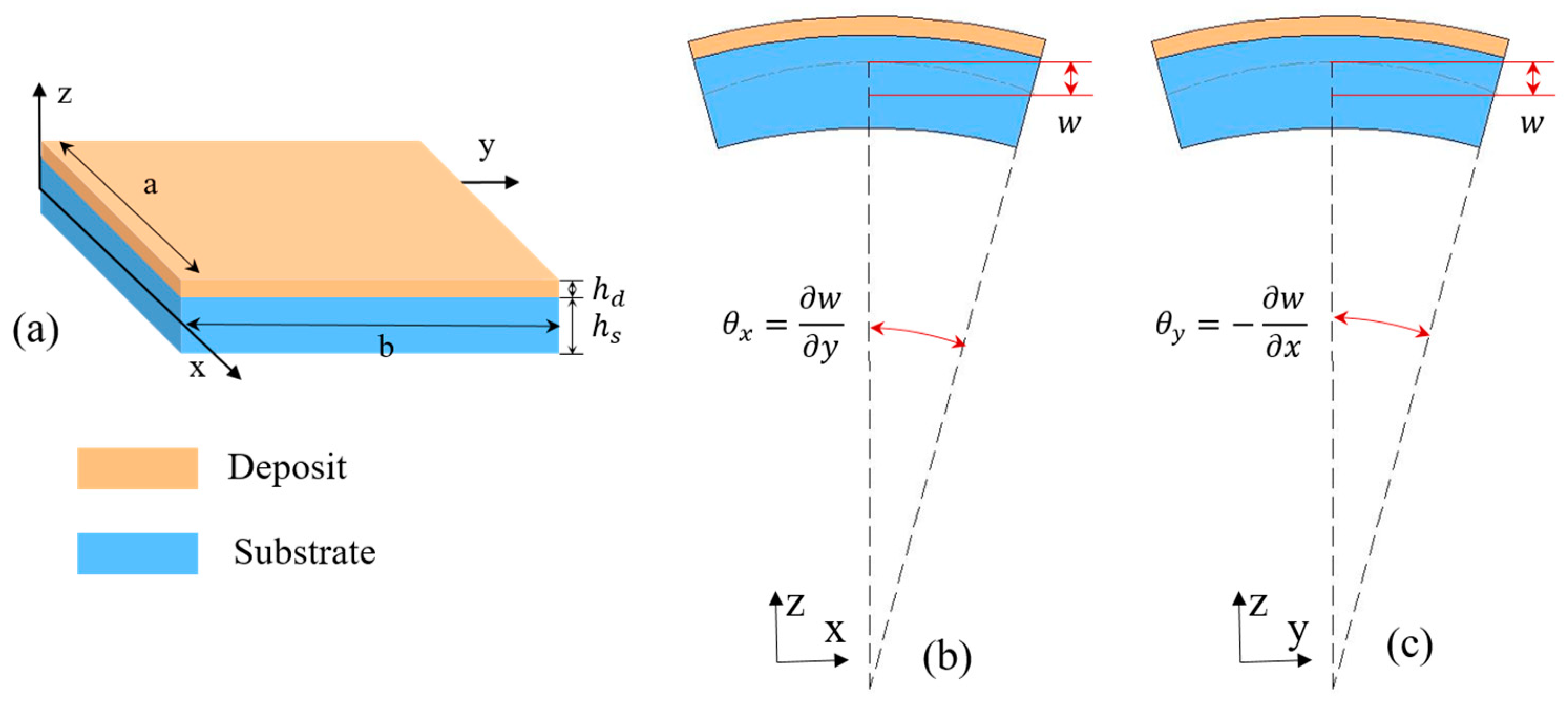
The geometry of a substrate-deposit system is shown in Figure A1a. The width of the system is a , the length is b , and the thickness is h = h d + h s , where h d and h s denote the thickness of the substrate and deposit. The origin of the coordinates is on the neutral plane of the substrate-deposit system. As shown in Figure A1b,c, the deformation of the substrate affected by the internal stress of the deposit mainly includes three types: (1) rotation of the neutral plane normal around the x-axis ( θ x = w y ), (2) rotation of the neutral plane normal around the y-axis ( θ y = w x ), (3) deflection of the neutral plane ( w = w ( x , y ) = w ( x , y , z = 0 ).
Figure A1. (a) The geometry of the substrate-deposit system. (b) Deformation of the substrate-deposit system in the xoz plane. (c) Deformation of the substrate-deposit system in the yoz plane.
Coatings 13 02031 g0a1
The deformation of the substrate-deposit system satisfies the Kirchhoff sheet theory without considering shear deformation, which contains three basic assumptions: (1) ignore the stress in the thickness direction ( σ z = 0 ) (2) assumption of the straight line ( γ x z = γ y z = 0 ) (3) No lateral deformation in the neutral plane ( u ( x , y , z = 0 ) = v ( x , y , z = 0 ) = 0 ).
From assumption (1), it can be known that
ε z = w z = 0
From assumption (2), it can be known that
γ y z = w y + v z = 0  
γ x z = w x + u z = 0  
From Equations (A2) and (A3), we can obtain
u z = w x
v z = w y  
Equations (A4) and (A5) integrate z , respectively, and it can be known that u z = 0 = 0 , v z = 0 = 0 from assumption (3). The relationship between u , v and w can be obtained as
u = z w x
v = z w y
Using the geometric equation, the strain components at each point in the plate can be obtained as
ε = ε x ε y γ x y = u x v y u y + v x
Substituting Equations (A6) and (A7) into Equation (A8), we can obtain
ε = ε x ε y γ x y = z 2 w x 2 2 w y 2 2 2 w x y  
The stress at each point in the plate can be obtained as
σ = σ x σ y τ x y = D ε = z D 2 w x 2 2 w y 2 2 2 w x y
where D is the elastic matrix of the plate.
D = E 1 μ 2 1 μ 0 μ 1 0 0 0 1 μ 2
During finite element calculation of plate bending, the plate is divided into a series of rectangular elements to obtain a discrete system to replace the original plate. For each element to have continuity in deflection and its slope at least at the nodes, the deflection and its first-order partial derivatives in the x and y directions must be specified as node displacements (or generalized displacements). The displacement array of node i is usually written as
δ i = w i θ x i θ y i = w i w y i w x i  
For rectangular elements, a natural coordinate system o ξ η is introduced to study element characteristics. Since each node of a rectangular element has three displacement components ( δ i ), one element has four nodes, as shown in Figure A2. There are twelve node displacement components, so we choose a polynomial with twelve parameters as the displacement model. The neutral plane w , rotation of the neutral plane normal around the x-axis θ x and rotation of the neutral plane normal around the y-axis θ y can be obtained as
w = a 1 + a 2 ξ + a 3 η + a 4 ξ 2 + a 5 ξ η + a 6 η 2 + a 7 ξ 3 + a 8 ξ 2 η + a 9 ξ η 2 + a 10 η 3 + a 11 ξ 3 η + a 12 ξ η 3  
θ x = w y = w b η = 1 b a 3 + a 5 ξ + 2 a 6 η + a 8 ξ 2 + 2 a 9 ξ η + 3 a 10 η 2 + a 11 ξ 3 + 3 a 12 ξ η 2
θ y = w x = w a ξ = 1 a ( a 2 + 2 a 4 ξ + a 5 η + 3 a 7 ξ 2 + 2 a 8 ξ η + a 9 η 2 + 3 a 11 ξ 2 η + a 12 η 3 )
where ξ = x a , η = y b .
Figure A2. Rectangular element nodes and their displacement components.
Coatings 13 02031 g0a2
Substituting the four-node coordinates ( ξ i , η i ) of the rectangular element into Equations (A13)–(A15), respectively, and obtaining twelve equations. Solving these twelve equations, obtaining a 1 to a 12 , and then substitute into Equation (A13), after merging and sorting, it can be rewritten into the following form:
w = N δ e
where N and δ e can be expressed as
N = N 1 N 2 N 3 N 4
δ e = δ 1 T δ 2 T δ 3 T δ 4 T T
If N is written as the general formula, which gives
N i = N i N x i N y i   ( i = 1,2 , 3,4 )  
where N i , N x i and N y i can be expressed as
N i = 1 + ξ 0 1 + η 0 2 + ξ 0 + η 0 ξ 2 η 2 8
N x i = b η i 1 + ξ 0 1 + η 0 1 η 2 8  
N y i = a ξ i ( 1 + ξ 0 ) ( 1 + η 0 ) ( 1 ξ 2 ) / 8  
where ξ 0 and η 0 are ξ 0 = ξ i ξ and η 0 = η i η , respectively.
Substituting Equation (A16) into geometric Equation (A19), the element strain can be expressed as a node displacement array as
ε = B i δ e = B 1 B 2 B 3 B 4 δ e
where B i can be expressed as
B i = z N i , x x N i , y y 2 N i , x y = z N i , ξ ξ a 2 N i , η η b 2 2 N i , ξ η a b = z a b b a N i , ξ ξ a b N i , η η 2 N i , ξ η
where N i , x x and N i , ξ ξ are 2 N i x 2 and 2 N i ξ 2 , respectively.
The element stiffness matrix can be written as
k = k 11 k 12 k 13 k 14 k 21 k 22 k 23 k 24 k 31 k 32 k 33 k 34 k 41 k 42 k 43 k 44
The formula for calculating the submatrix is
k i j = B i T D B j d x d y d z = h 2 h 2 1 1 1 1 B i T D B j a b d ξ d η d ζ
Substituting Equations (A11) and (A24) into the above equation, and integrating with z, so we have
k i j = D a b 1 1 1 1 b 2 a 2 N i , ξ ξ T N j , ξ ξ + μ N i , ξ ξ T N j , η η + μ N i , η η T N j , ξ ξ + a 2 b 2 N i , η η T N j , η η + 2 ( 1 μ ) N i , ξ η T N j , ξ η d ξ d η
where D can be expressed as
D = E h 3 12 1 μ 2  
It is generally considered that D is the bending stiffness of the elastic substrate. However, it ignores the influence of the length and width of the substrate. In this paper, D a b is used to represent the bending stiffness of the elastic substrate ( B s ).
B s = D a b = E h 3 12 ( 1 μ 2 ) ( a b )  

References

  1. Chason, E. Stress Measurement in Thin Films Using Wafer Curvature: Principles and Applications. In Handbook of Mechanics of Materials; Springer: Singapore, 2018; pp. 1–33. [Google Scholar]
  2. Pureza, J.; Lacerda, M.; De Oliveira, A.; Fragalli, J.; Zanon, R. Enhancing accuracy to Stoney equation. Appl. Surf. Sci. 2009, 255, 6426–6428. [Google Scholar] [CrossRef]
  3. Stoney, G.G. The Tension of Metallic Films deposited by Electrolysis. Proc. R. Soc. Lond. 1909, 82, 172–175. [Google Scholar]
  4. Hearne, S.J.; Floro, J.A. Mechanisms inducing compressive stress during electrodeposition of Ni. J. Appl. Phys. 2005, 97, 014901. [Google Scholar] [CrossRef]
  5. Takehiro Kume, S.E. Hidekazu Mimura, Development of internal stress measurement technique for Ni electroforming using Shack–Hartmann sensor. Int. J. Electr. Mach. 2016, 21, 25–30. [Google Scholar] [CrossRef]
  6. Kume, T.; Egawa, S.; Yamaguchi, G.; Mimura, H. Influence of Residual Stress of Electrodeposited Layer on Shape Replication Accuracy in Ni Electroforming. Procedia CIRP 2016, 42, 783–787. [Google Scholar] [CrossRef]
  7. Qiang, J.; Luo, K.; Dong, Y.; Jiang, B.; Drummer, D.; Roth, B. In Situ Stress Measurement of Ni Electrodeposition Using Lateral Shearing Interferometry. J. Electrochem. Soc. 2020, 167, 162504. [Google Scholar] [CrossRef]
  8. Besnard, A.; Ardigo, M.R.; Imhoff, L.; Jacquet, P. Curvature radius measurement by optical profiler and determination of the residual stress in thin films. Appl. Surf. Sci. 2019, 487, 356–361. [Google Scholar] [CrossRef]
  9. Mezin, A. Coating internal stress measurement through the curvature method: A geometry-based criterion delimiting the relevance of Stoney’s formula. Surf. Coat. Technol. 2006, 200, 5259–5267. [Google Scholar] [CrossRef]
  10. Abadias, G.; Daniel, R. Stress in physical vapor deposited thin films: Measurement methods and selected examples. In Handbook of Modern Coating Technologies; Elsevier: Amsterdam, The Netherlands, 2021; pp. 359–436. [Google Scholar]
  11. Freund, L.; Floro, J.; Chason, E. Extensions of the Stoney formula for substrate curvature to configurations with thin substrates or large deformations. Appl. Phys. Lett. 1999, 74, 1987–1989. [Google Scholar] [CrossRef]
  12. Shiri, S.; Ashtijoo, P.; Odeshi, A.; Yang, Q. Evaluation of Stoney equation for determining the internal stress of DLC thin films using an optical profiler. Surf. Coat. Technol. 2016, 308, 98–100. [Google Scholar] [CrossRef]
  13. Guyot, N.; Harmand, Y.; Mezin, A. The role of the sample shape and size on the internal stress induced curvature of thin-film substrate systems. Int. J. Solids Struct. 2004, 41, 5143–5154. [Google Scholar] [CrossRef]
  14. Graciano, V.; Bertocci, U.; Stafford, G. In-Situ Stress Measurements during Cobalt Electrodeposition. J. Electrochem. Soc. 2019, 166, 3246–3253. [Google Scholar] [CrossRef]
  15. Fayette, M.; Bertocci, U.; Stafford, G. In Situ Stress Measurements during Cobalt Electrodeposition on (111)-Textured Au. J. Electrochem. Soc. 2016, 163, D146–D153. [Google Scholar] [CrossRef]
  16. Yu, H.; Thompson, C. Grain growth and complex stress evolution during Volmer-Weber growth of polycrystalline thin films. Acta Mater. 2014, 67, 189–198. [Google Scholar] [CrossRef]
  17. Song, C.; Du, L.; Li, X.; Li, Y.; Qi, L.; Li, Y. Residual stress modeling and analysis for micro electroforming layer. Microsyst. Technol. 2017, 23, 4709–4716. [Google Scholar] [CrossRef]
  18. Song, C.; Du, L.; Zhao, W.; Zhu, H.; Zhao, W.; Wang, W. Effectiveness of stress release geometries on reducing residual stress in electroforming metal microstructure. J. Micromechan. Microeng. 2018, 28, 045010. [Google Scholar] [CrossRef]
  19. Chen, H.; Huang, C.; Cheng, P. Stress mechanisms of SiO2 and Nb2O5 thin films sputtered on flexible substrates investigated by finite element method. Surf. Coat. Technol. 2018, 344, 449–457. [Google Scholar] [CrossRef]
  20. Nejhad, M.; Pan, C.; Feng, H. Intrinsic strain modeling and residual stress analysis for thin-film processing of layered structures. J. Electron. Packag. 2003, 125, 4–17. [Google Scholar] [CrossRef]
  21. Song, C.; Du, L.; Qi, L.; Li, Y.; Li, X.; Li, Y. Residual stress measurement in a metal microdevice by micro Raman spectroscopy. J. Micromechan. Microeng. 2017, 27, 7. [Google Scholar] [CrossRef]
  22. Floro, J.; Chason, E.; Cammarata, R.; Srolovitz, D. Physical origins of intrinsic stresses in Volmer-Weber thin films. MRS Bull. 2002, 27, 19–25. [Google Scholar] [CrossRef]
  23. Abadias, G.; Simonot, L.; Colin, J.; Michel, A.; Camelio, S.; Babonneau, D. Volmer-Weber growth stages of polycrystalline metal films probed by in situ and real-time optical diagnostics. Appl. Phys. Lett. 2015, 107, 183105. [Google Scholar] [CrossRef]
  24. Freund, L.B. Substrate curvature due to thin ®lm mismatch strain in the nonlinear deformation range. J. Mech. Phys. Solids 2000, 48, 1159–1174. [Google Scholar] [CrossRef]
  25. Huang, Y.; Rosakis, A. Extension of Stoney’s formula to nonuniform temperature distributions in thin film/substrate systems. J. Mech. Phys. Solids 2005, 53, 2483–2500. [Google Scholar] [CrossRef]
  26. Feng, X.; Huang, Y.; Rosakis, A.J. Stresses in a multilayer thin film/substrate system subjected to nonuniform temperature. J. Appl. Mech. Trans. Asme 2008, 75, 021022. [Google Scholar] [CrossRef]
  27. Blech, I.; Blech, I.; Finot, M. Determination of thin-film stresses on round substrates. J. Appl. Phys. 2005, 97, 113525. [Google Scholar] [CrossRef]
  28. Finot, M.; Blech, I.; Suresh, S.; Fujimoto, H. Large deformation and geometric instability of substrates with thin-film deposits. J. Appl. Phys. 1997, 81, 3457–3464. [Google Scholar] [CrossRef]
  29. Freund, L.; Suresh, S. Thin Film Materials: Stress, Defect Formation, and Surface Evolution; Cambridge University Press: Cambridge, UK, 2003. [Google Scholar]
  30. Shield, T.; Kim, K. Beam theory models for thin film segments cohesively bonded to an elastic half space. Int. J. Solids Struct. 1992, 29, 1085–1103. [Google Scholar] [CrossRef]
  31. Hutchinson, J.; Suo, Z. Mixed Mode Cracking in Layered Materials. In Advances in Applied Mechanics; Hutchinson, J.W., Wu, T.Y., Eds.; Elsevier: Amsterdam, The Netherlands, 1991; pp. 63–191. [Google Scholar]
  32. Zhang, Y. Extended Stoney’s formula for a film-substrate bilayer with the effect of interfacial slip. J. Appl. Mech. Trans. Asme 2008, 75, 011008. [Google Scholar] [CrossRef]
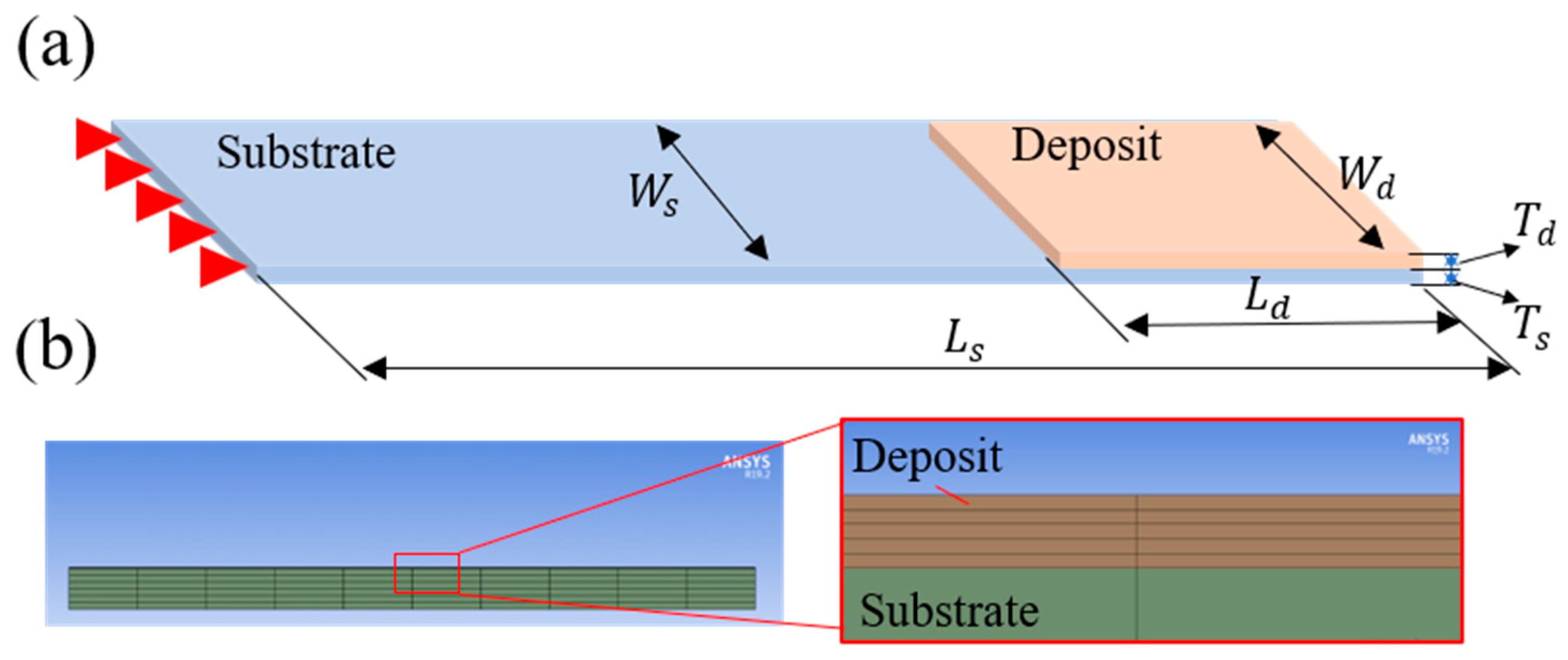
Figure 1. Schematic illustration of the model for the simulation. (a) Geometric model, the left is fixed, and (b) Mesh of the model.
Coatings 13 02031 g001
Figure 2. The workflow of the simulation by the ERT method.
Coatings 13 02031 g002
Figure 3. The curvature radius of a substrate-deposit system. (a) Stress and deformation value extracted by paths (lines of A-1 to A-2 and B-1 to B-2 represent x and y directions, respectively). (b) Schematic illustration for the calculation method of curvature radius.
Coatings 13 02031 g003
Figure 4. A self-developed electrodeposition system for stress measurement. (a) A schematic of the in situ stress measurement apparatus, (b) A spherical sample and their phase maps. (c) An ellipsoidal sample and their phase map. Where k x and k y represent the curvature of the sample in x- and y-directions, respectively. Cloud map colors indicate phases. Red color indicates large displacement, and blue represents that the displacement is zero. The spherical sample indicates that the deformation displacement is the same in all directions, and the ellipsoidal indicates the presence of nonlinear phenomena.
Coatings 13 02031 g004
Figure 5. The curvature radius as a function of time with different directions. The widths of the substrates were (a) 15 mm, (b) 10 mm, and (c) 5 mm, respectively.
Coatings 13 02031 g005
Figure 6. In situ stress measurement of Ni electrodeposition with different substrate widths. (a,d,g) The curvature radius as a function of time with different directions (Insets show phase map at different times. (b,e,h) The average stress is a function of depositing thickness in different directions. (c,f,i) The surface morphology after electrodeposition. The widths of (ac), (df), and (gi) are 15 mm, 10 mm, and 5 mm, respectively.
Coatings 13 02031 g006
Figure 7. Curvature radius and stress of the deposit in the simulation. (a) The radius of curvature as a function of substrate width for x and y directions; (b) The average stress plotted as a function of substrate width for Stoney’s formula calculation and simulation ( T r e f was 325.15 K). (c) The radius of curvature as a function of equivalent reference temperature ( T r e f ) for x and y directions. (d) The average stress as a function of T r e f for calculation using Stoney’s formula and simulation (The substrate width is 5 mm).
Coatings 13 02031 g007
Figure 8. Total stress on different substrate sizes for (a) the x-direction and (b) the y-direction; and (c) schematic of a deposit–substrate system with a free edge. The enlarged figure shows the distribution of the interfacial shear stress ( q ( x ) ).
Coatings 13 02031 g008
Table 1. Material properties used in the simulation.
MaterialsElastic Modulus/GPaPoisson RatioCoefficient of Thermal Expansion/°C−1
Nickel2100.311.33 × 10−5
Quartz glass550.255.5 × 10−7
Table 2. Size of deposits and substrates in simulations and experiments.
DepositsSubstrates
Length
( L d / m m )
Width
( W d / m m )
Thickness
( T d / m m )
Length
( L s / m m )
Width
( W s / m m )
Thickness
( T s / m m )
1550.018050.3
1010
1515
Disclaimer/Publisher’s Note: The statements, opinions and data contained in all publications are solely those of the individual author(s) and contributor(s) and not of MDPI and/or the editor(s). MDPI and/or the editor(s) disclaim responsibility for any injury to people or property resulting from any ideas, methods, instructions or products referred to in the content.