Abstract
This work presents a novel trusted LC voltage-controlled oscillator (VCO) with an embedded compact analog Physically Unclonable Function (PUF) used for authentication. The trusted VCO is implemented in a 1P9M 65 nm standard CMOS process and consumes 1.75 mW. It exhibits a measured phase noise (PN) of −104.8 dBc/Hz @ 1 MHz and −132.2 dBc/Hz @ 10 MHz offset, resulting in Figures of Merit (FoMs) of 191.7 dBc/Hz and 199.1 dBc/Hz, respectively. With the measured frequency tuning range (TR) of ~5.5 GHz, the FoM with tuning (FoMT) reaches 197.6 dBc/Hz and 205.0 dBc/Hz at 1 MHz and 10 MHz offset, respectively. The analog PUF consists of CMOS cross-coupled pairs in the main VCO to change analog characteristics. Benefiting from the impedance change and parasitic capacitance of the cross-coupled pairs, the AC and DC responses of the VCO are utilized for multiple responses for each input. The PUF consumes 0.83 pJ/bit when operating at 1.5 Gbps. The proposed PUF exhibits a measured Inter-Hamming Distance (HD) of 0.5058b and 0.4978b, with Intra-HD reaching 0.0055b and 0.0053b for the current consumption and fosc, respectively. The autocorrelation function (ACF) of 0.0111 and 0.0110 is obtained for the current consumption and fosc, respectively, at a 95% confidence level.
1. Introduction
High-speed wireless communication is becoming a necessity for modern connectivity solutions [1]. With the introduction of the 5G new radio (NR) standard, millimeter wave (mm-Wave) frequency bands are becoming accessible to facilitate such high-speed communications in today’s spectrum-congested network [1]. However, migration to higher frequency bands complicates efforts to reduce the power consumption in wireless data links used for many consumer and medical applications. In addition to low power consumption, maintaining a high level of security and trust is critical in such links to protect sensitive data and preserve user privacy [2,3]. This requirement further complicates the design of low-power high-data throughput wireless transceivers operating at mm-Wave frequency bands.
Depending on the threat type and application, creating an end-to-end secure and trustworthy wireless communication link calls for the inclusion of security features at all levels, including wireless transceivers [4,5,6]. Unlike data security, which can be accomplished using encryption performed in the digital backend, a trusted wireless transceiver should contain security features in the Radio Frequency Front End (RFFE) for proper authentication. To minimize the energy, area, and delay overhead, it is more efficient to choose an embedded approach in which the trust features are integrated into key sub-blocks within the RFFE.
Designing the proper trust feature for authentication requires knowledge of the main attack vectors in an RFFE. Hardware Trojans (HTs) [5,6] and Side-Channel Attacks (SCAs) [4,7,8] are the main threats to the RFFE. There are a number of authentication solutions that protect devices against HTs [4,5,6,7,8,9]. Among them, analog PUFs are more suitable for inclusion within RFFEs due to their small size, low complexity, and ease of integration with analog circuits [10,11,12,13,14,15]. They are particularly useful in authenticating RFFEs built with high-performance wide-bandgap (WBG) technologies, such as GaAs and GaN [16], where the implementation of high-density logic/memory needed for digital PUFs is challenging. Analog PUFs typically rely on the complexity of the Challenge–Response Pair (CRP) instead of only increasing the number of CRPs [10]; they leverage transistors’ intrinsic random process variations to generate a unique fingerprint needed for authentication. Due to their small CRP size, analogs are typically categorized as weak PUFs. However, the complexity of the CRP mechanism beyond a simple binary stream seen from digital PUFs may help with increasing the entropy [9,10,11,12]. A few examples are printed differential circuits [11], current-steering digital-to-analog converters (DACs), and VCOs [13].
Presently, nearly all analog PUFs are designed as standalone blocks and are included on the chip as a separate module. While easier to develop, these solutions have a negative impact on the overall power consumption, chip area, and latency in the transceiver. Moreover, analog PUFs typically exhibit low entropy due to their small CRP space [10], further limiting their usefulness for device authentication. To mitigate these concerns, this work proposes to integrate the analog PUF within key transceiver blocks, such as the VCO, to facilitate the authentication process in the wireless transceiver. The resulting low-power 24.6-to-30.1 GHz trusted LC VCO benefits from a custom analog PUF consisting of multiple NMOS and PMOS cross-coupled pairs, which are connected to the main CMOS cross-coupled pair. When properly excited, the impedance across the main cross-coupled CMOS pair varies [14], changing the VCO characteristics. The overall power consumption of the VCO also changes. This change is manifested in variations in the VCO’s DC and AC performance metrics, such as the current consumption, fosc, amplitude, and PN, resulting in increased entropy with the same number of challenges. The remainder of this paper is structured as follows. Section 2 describes the threat model and provides more details on the design of the embedded analog PUF. The proposed low-power trusted LC VCO design is presented in Section 3 and is followed by the characterization results in Section 4. Section 5 provides the concluding remarks.
2. RFFE Threats and Embedded Analog PUF Design
The Integrated Circuit (IC) supply chain (including the fabrication process) is an inherently untrustworthy process that exposes hardware-induced vulnerabilities. For example, an attacker can place malware circuits on the die during the fabrication process to create a backdoor [4] or interrupt the main function of the IC [5]. Or, an attacker may gain information about the design of the RFFE by accessing mask sets during the IC fabrication process and be able to directly hack the RFFE and obtain the raw data [7,8,9]. Major threats to the RFFE and embedded PUF solutions to protect against such threats are discussed in this section.
2.1. Security Threats in RFFEs
Security threats or attack vectors for hardware are categorized into three classes [4,5]: non-invasive, semi-invasive, and invasive. The difference between classes is defined by the equipment and attackers’ approach [4]. HTs and SCAs are the main security threats for RFFEs; HTs can be easily implanted using all three specified methods and compromise the RFFE [4,5,6]. An attacker can even minimize scars and marks caused by physical altercations to complicate post-silicon detection efforts performed by the defender. SCAs monitor key IC signatures, such as the power consumption or EM radiation, to gather information about the design, and, hence, do not need access to the digital backend for executing a successful attack [7]. Taking advantage of hardware security primitives employed in PUF blocks, the aforementioned threats can be detected and neutralized. These blocks leverage random fluctuations in the production process, such as IC process artifacts, to create unclonable and inherent device-specific identifiers of the device. Using PUFs, a challenge applied to the input will produce a unique output, creating a complex CRP that can be used for device authentication. For an RFFE operating at mm-Wave, an analog PUF is easier to implement since it does not require access to the digital backend and additional auxiliary circuits (such as clock generators and memory) needed for the proper operation of digital PUFs [5]. They will also occupy a smaller area and have less delay [10,11,12,13,14,15].
2.2. Embedded Analog PUFs for RFFEs
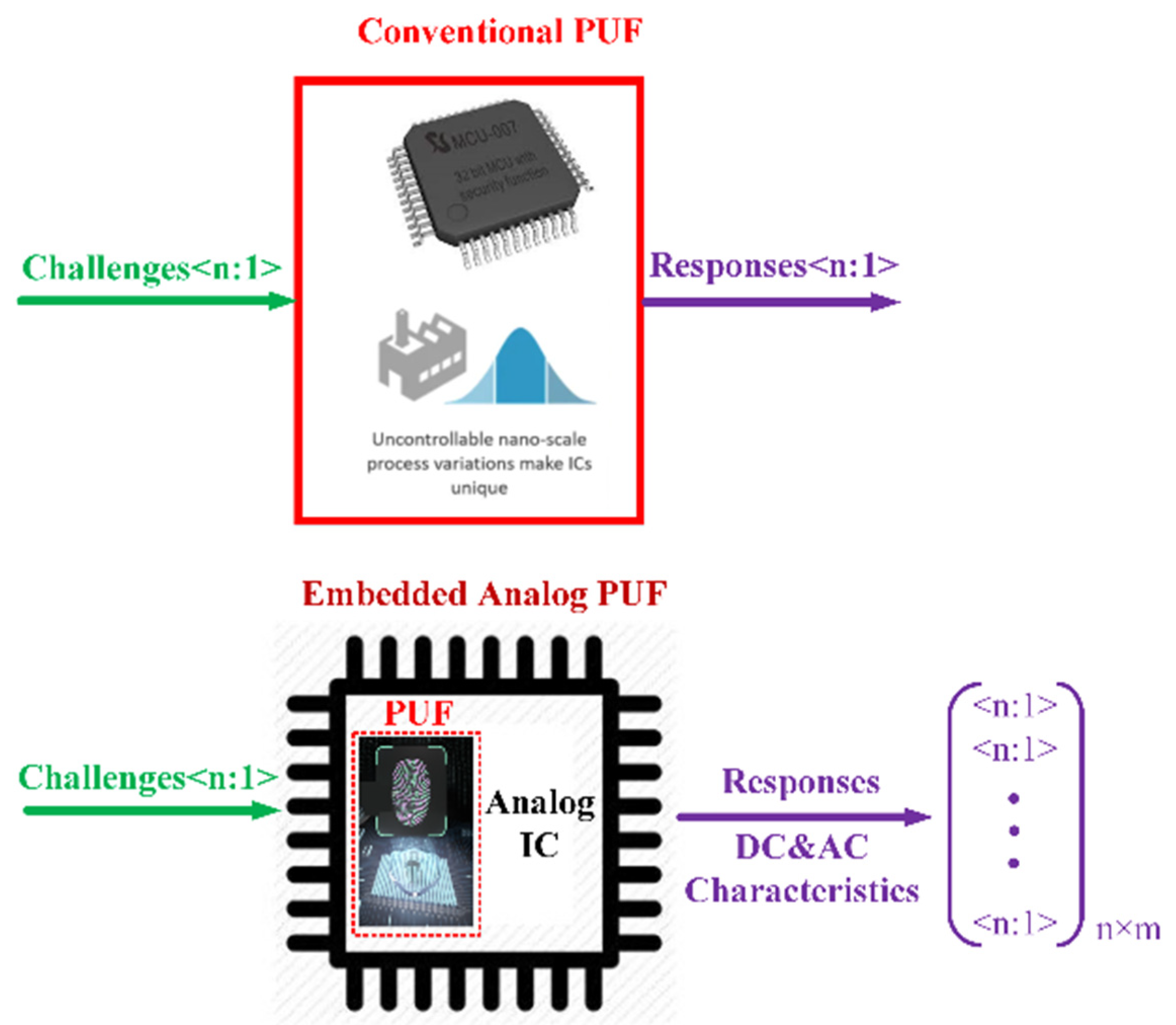
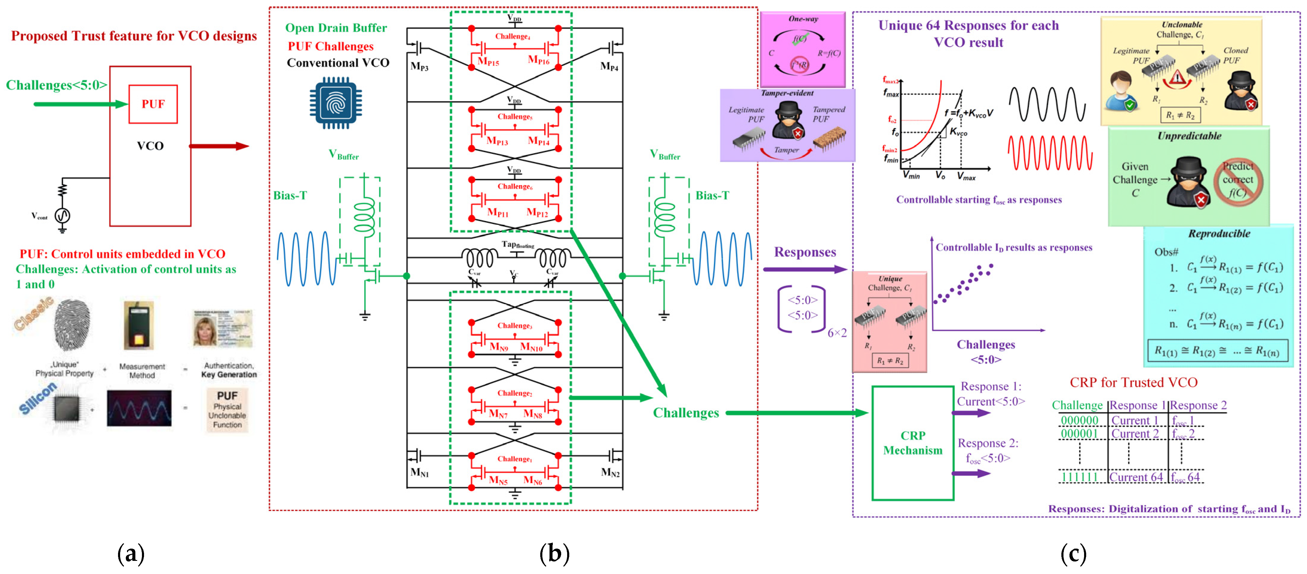
Analog PUFs usually suffer from low entropy due to their small CRP space. To solve this problem, an embedded PUF solution is proposed. The proposed PUF uses both DC and AC characteristics of a radio frequency (RF) circuit to enhance the CRP space without increasing the complexity or length of the input challenge. The number of input challenges is defined as n, as shown in Figure 1. In conventional PUF designs, n input challenges correspond to n output responses (Figure 1). However, the proposed PUF generates multiple responses for a given challenge (e.g., m responses). In this way, an n × 1 long input generates an n × m long output response, increasing the CRP space by a factor of m compared to a conventional PUF solution (Figure 1). The concept of embedded PUF has been introduced in the early 2000s as a more compact and integration-friendly alternative to conventional PUFs [10]. However, these designs require a more complicated CRP generation and detection system due to inaccuracies caused by the miniaturization of the PUF core, which is needed for integration with the RF/analog block [2,3,4,5,6,7,8,9,10]. For example, transistor random mismatch is greatly influenced by the area of the device; the larger the area, the more accurate the device geometry can be predicted, leading to the opportunity to design a more accurate PUF with higher entropy. However, utilizing this phenomenon to increase the entropy in the PUF requires a large area for the transistors and a very accurate interface circuit consisting of ultra-low offset comparators and amplifiers. On the other hand, leveraging the high-frequency characteristics of an RF circuit helps break this paradigm with minimal penalty to the size, power consumption, and the size of the RFFE. In this prototype, an innovative embedded analog PUF technique is introduced in the VCO (Figure 2a–c). The CRPs are based on the DC characteristics and the frequency response of the VCO. The current consumption and fosc are sensitive to process artifacts and parasitics, and, hence, can be used for authentication. By adding additional cross-coupled pairs whose device sizes are slightly different than the main pair, in parallel to the main CMOS cross-coupled pair, the VCO current consumption changes (Figure 2b). The additional parasitic capacitance from the cross-coupled pair also causes a shift in the fosc. By adjusting the gate-source voltage (VGS) in each pair or adding multiple pairs with different W/L, the variation in the current consumption and fosc can be controlled, creating a proper CRP space for authentication. The additional cross-coupled pairs can be turned off so as to not impact the performance of the VCO during the normal operation of the VCO. This is easily performed by pulling up or down the gate voltages for the PMOS and NMOS pairs, respectively. Unlike conventional PUFs, where the input and output vectors have similar dimensions, here, each challenge vector generates multiple response vectors, of which the current consumption and fosc are used in this proof-of-concept prototype. The proposed prototype uses 64 challenges (six bits: 3-bit NMOS and 3-bit PMOS), resulting in 128 (27) output responses (Figure 2c). Responses of the 6-bit challenges are analog values but they are digitized for PUF characterization and analysis. In this work, responses are converted into codewords for PUF characterization and analysis. The codeword generation from responses is discussed as part of the PUF characterization efforts discussed in Section 4.
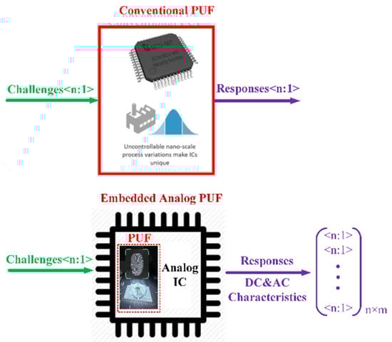
Figure 1.
CRPs in conventional and embedded analog PUFs.
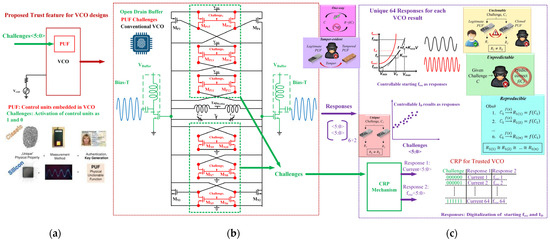
Figure 2.
Block diagram of the proposed design showing (a) the PUF concept, (b) the VCO schematic, and (c) the CRP mechanism.
3. Design of the Trusted CMOS LC VCO
The proposed trusted LC VCO uses a complementary (i.e., CMOS) cross-coupled topology without a tail current source to maximize the output swing (Figure 2b). A conventional CMOS LC VCO (CVCO) is also implemented on the same chip for performance comparison. The VCO uses open drain buffers to interface with the measurement equipment. Optimum LC VCO design heavily relies on the bias current (ID) because it determines the mode of operation, i.e., the voltage-limited or current-limited regime [17,18]. In addition to the gm of the NMOS and PMOS cross-coupled pairs, the LC tank plays a key role in the power consumption, PN, and TR performance of an LC VCO, requiring a careful design of tank components, particularly the inductance [17,18,19]. Knowing that the PN is proportional to (Ltank)2 [19], a small inductance with the highest quality factor (Q) is chosen for the tank. Moreover, the TR is inversely proportional to the Ltank, further incentivizing the use of a small inductor. To further increase the inductor Q and save chip area, the VCOs use differential inductors with a floating center tap [19]. The 420 pH inductor designed for the CVCO exhibits a Q~15 at 28 GHz with 69.2 GHz self-resonance frequency (SRF), while the 315 pH inductor designed for the trusted VCO (Figure 3) shows Q~17.2 at 28 GHz with SRF > 80 GHz. The trust features are embedded within the VCO as six cross-coupled pairs, three NMOS and three PMOS. These additional cross-coupled pairs are only used for authentication; they are turned off during the normal operation of the VCO and primarily act as parasitic capacitance in this mode.
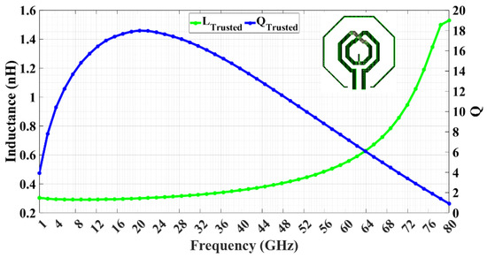
Figure 3.
Q, L, and the layout of the inductor used in the proposed design.
The design procedure for the proposed trusted LC VCO begins with the choice of topology. Here, a CMOS cross-coupled pair without a tail current source is chosen to maximize the output swing and increase the effective transconductance (Gm). Then, the trust features that can be embedded into the VCO core are identified. An important consideration for the design of the embedded PUF is the compatibility of the PUF architecture with the VCO core architecture without a significant hit to the power consumption and size of the VCO. At the same time, the PUF should generate the required entropy for the authentication process [10]. For this design, a cross-coupled PUF topology, which relies on the variation in the impedance, is utilized to generate the change in the current consumption and the oscillation frequency as the unique identifiers for the authentication process. During the normal operation, the trust features are disabled, leaving only the main cross-coupled pair active, which resembles a conventional CMOS LC VCO. In this case, the VCO core design procedure will be straightforward. The cross-coupled pair generates the required Gm to compensate for the loss of the LC tank (modeled by Rp). The oscillation frequency, ω, is set by the tank as follows:
where Gm is the total transconductance in the system that is equal to the transconductance of a CMOS device (gm), is equivalent parallel resistance of the LC tank used in the VCO, is the total equivalent capacitance of the tank, is the total parasitic capacitance from a cross-coupled pair, is the capacitance from tuning varactors, Cpd is the parasitic capacitance from the inactive cross-coupled pairs used for the PUF, is the parasitic capacitance from the active cross-coupled pairs used for the PUF, is the parasitic capacitance from the CMOS devices that is equal to , and and are the gate-source and drain-source MOS capacitance of the CMOS device. In this design, the power consumption is reduced by increasing the Q of the inductor to generate a larger Rp, leading to a smaller required Gm for oscillation. Moreover, the stacked combination of NMOS and PMOS pairs used in the VCO core and the PUF allows for reusing the current from the PMOS into the NMOS pair, generating larger overall Gm without increasing the current consumption. When the VCO operates in authentication mode, additional cross-coupled pairs are enabled. Consequently, the current consumption and the frequency are lowered due to larger parasitic capacitance from these pairs.
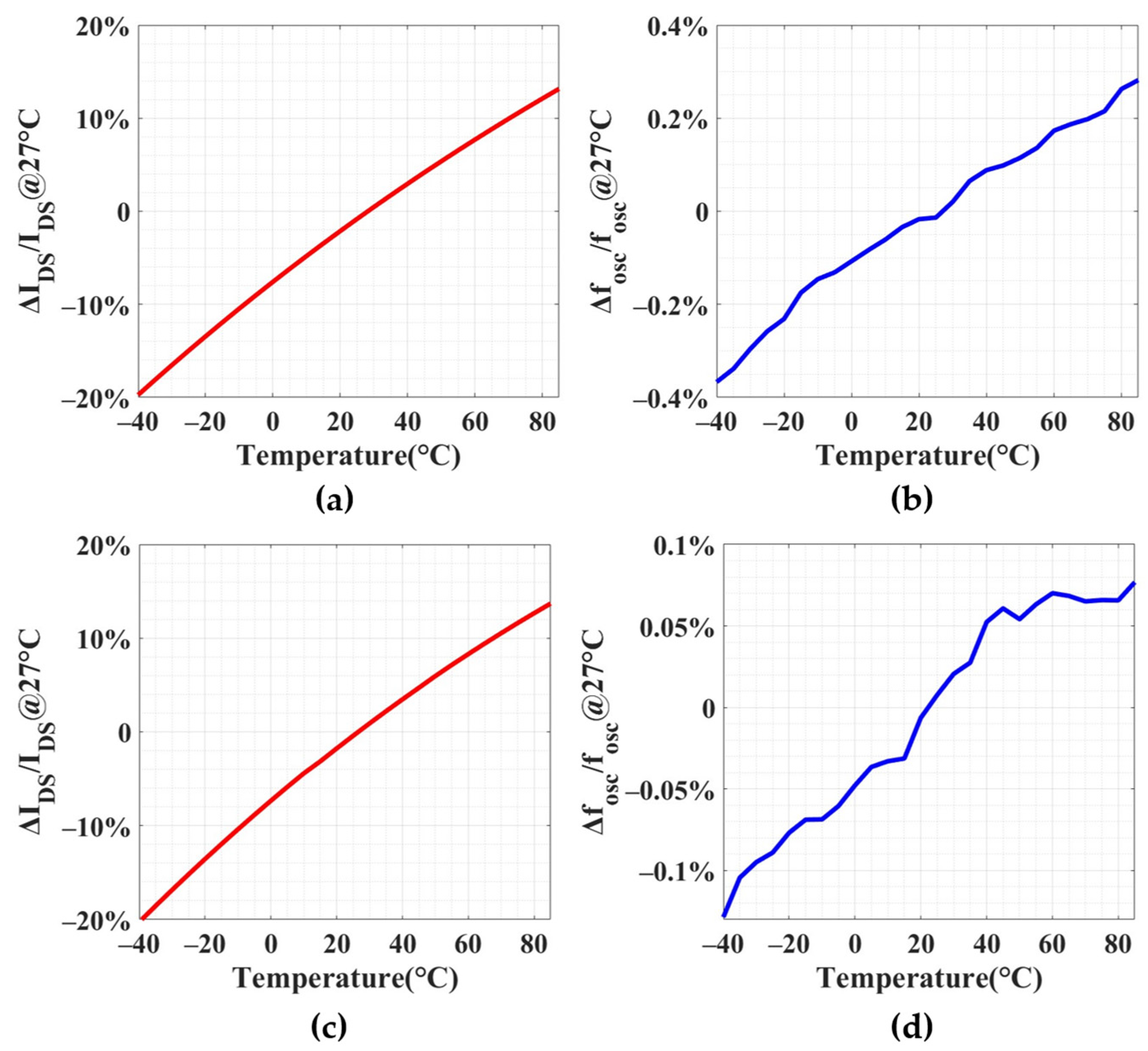
IC fabrication is an electromechanical process that is prone to process variation and mismatch, of which the device mismatch is the main source of entropy in the proposed analog PUF [5]. However, the effect of the temperature variation on the performance of the analog CMOS circuits cannot be ignored and should also be investigated for the proposed analog PUF. Figure 4 shows changes in the simulated current consumption and fosc when the temperature is varied from −40 °C to 85 °C for the first challenge, 000000, and the last challenge, 111111. The changes to the current consumption are reasonable and follow the MOS threshold variation with temperature. Since the change in current consumption is almost linear, it can be easily compensated for using adaptive biasing (i.e., changing the supply with temperature) or calibrated out in post-measurement calculations. The changes to the fosc are very small (<±0.1%), as expected, since fosc is mainly determined by the frequency of the LC tank whose variations with temperature are negligible. Expecting a unique response for each input challenge, the accuracy of the analog PUF should be investigated. The amount of mismatch and its impact on the PUF resolution can be found by performing post-layout Monte Carlo (MC) simulations on the trusted VCO when the embedded analog PUF is turned on.
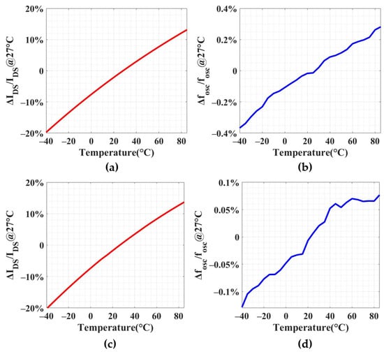
Figure 4.
Changes to the normalized (a) current consumption (red) and (b) fosc for the first challenge (blue), 000000, when the temperature is varied; a similar trend is observed for (c) current consumption (red) and (d) fosc (blue) for the last challenge, 111111.
Figure 5 shows the Probability Distribution Function (PDF) of the current consumption and fosc at −40 °C, 27 °C (room temperature), and 85 °C for the first challenge, 000000. As expected, the PDF of the output results resembles those of a Gaussian/normal function for all three temperatures. For a 200-sample MC simulation, the current consumption and fosc show reasonable variations with the standard deviation (σ)~67 µA and ~15 MHz at 27 °C (Figure 5). The PDF also remains close to Gaussian when temperature changes with σ for the current consumption and fosc~70 µA and ~14 MHz at −40 °C, and ~63 µA and ~22 MHz at 85 °C, respectively. The MC simulations are repeated for the last challenge, 111111, showing a similar Gaussian/normal behavior (Figure 6). The MC results are then used to evaluate the randomness of the proposed PUF using the Hamming Distance (HD) function, which is a metric to show the difference between two data strings. There are two HD measurements: Intra-HD and Inter-HD. Intra-HD measures the randomness of a single PUF design (or a single chip) when one bit of the input challenge changes, while the Inter-HD demonstrates the randomness between different PUF designs (or different chips) when the same challenge is applied to the PUFs. For each challenge, a single MC simulation can be used to find Inter-HD since MC simulations based on the device mismatch show the PUF output difference between different samples (i.e., dies). Ideally, the Intra-HD and Inter-HD of a PUF should be 0 and 0.5, respectively. Simulating Intra-HD in an ideal simulation environment where circuit parameters, the supply voltage, biasing, and output load do not experience any variation during the simulation is very challenging since the simulator only uses the mathematical models for the analysis. To emulate a realistic environment for Intra-HD simulations, reasonable uncertainty is added to the test bench by adding randomness to the DC sources and temperature. The DC sources used in the test bench are randomly varied by considering ±5 mV error. This is consistent with testing conditions in our lab where the DC voltages are set manually. In addition to variations of the DC voltages, the temperature randomly varied from room temperature by ±1 °C (from 26 °C to 28 °C) to emulate fluctuations in the room temperature during the measurement. Figure 7a–f show the Inter-HD and Intra-HD results for the current consumption and fosc at −40 °C, 27 °C, and 85 °C based on the 200-sample post-layout MC simulations. Since the PDF of the current consumption and fosc are reasonably close to Gaussian for both challenges, as shown in Figure 5 and Figure 6, the Inter- and Intra-HD results are only presented for the first challenge, 000000. Ideally, Inter-HD for PUFs should be 0.5 and Intra-HD should be 0 [10,11,12,13,14,15]. The challenge for defining Inter-HD and Intra-HD is to create accurate and reliable bit representations (i.e., codeword) for responses. Codeword generation for this work is based on the Huffman coding algorithm [20] and will be discussed in more detail in Section 4. Using these codewords, the Inter-HD of the simulated responses are 0.4997 at −40 °C, 0.4995 at 27 °C, and 0.5004 at 85 °C for the current consumption, and 0.5010 at −40 °C, 0.4991 at 27 °C, and 0.5090 at 85 °C for fosc, respectively. The Intra-HD of the simulated responses are 0.0107 at −40 °C, 0.0085 at 27 °C, and 0.0092 at 85 °C for the current consumption, and 0.0036 at −40 °C, 0.0029 at 27 °C, and 0.0043 at 85 °C for fosc, respectively. Both simulated Intra- and Inter-HD are very close to the ideal values for a PUF.
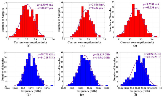
Figure 5.
PDFs of the current consumption and fosc of the proposed trusted VCO for the first challenge, 000000; PDF of the current consumption (red) at (a) −40 °C, (b) 27 °C, (c) 85 °C, and PDF of fosc (blue) at (d) −40 °C, (e) 27 °C, (f) 85 °C.
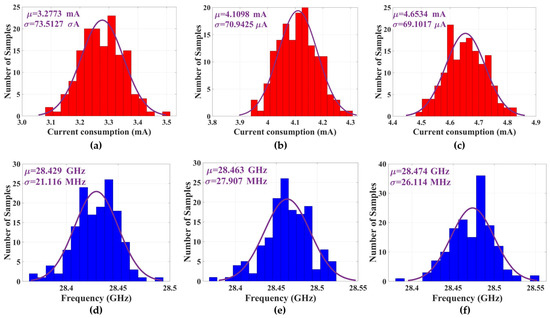
Figure 6.
PDFs of the current consumption and fosc of the proposed trusted VCO for the last challenge, 111111; PDF of the current consumption (red) at (a) −40 °C, (b) 27 °C, (c) 85 °C, and PDF of fosc (blue) at (d) −40 °C, (e) 27 °C, (f) 85 °C.
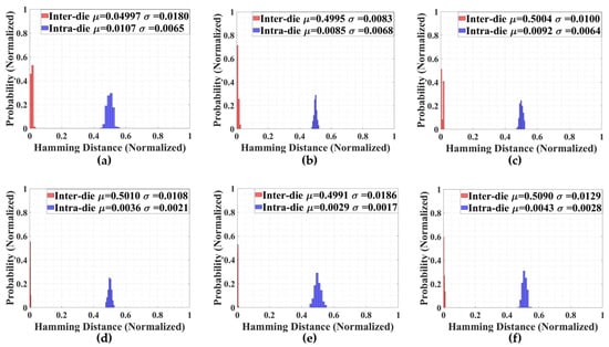
Figure 7.
Intra-HD, and Inter-HD of the proposed trusted VCO for the current consumption at (a) −40 °C, (b) 27 °C, and (c) 85 °C, along with those of fosc at (d) −40 °C, (e) 27 °C, and (f) 85 °C for the first challenge, 000000.
4. Measurement Results
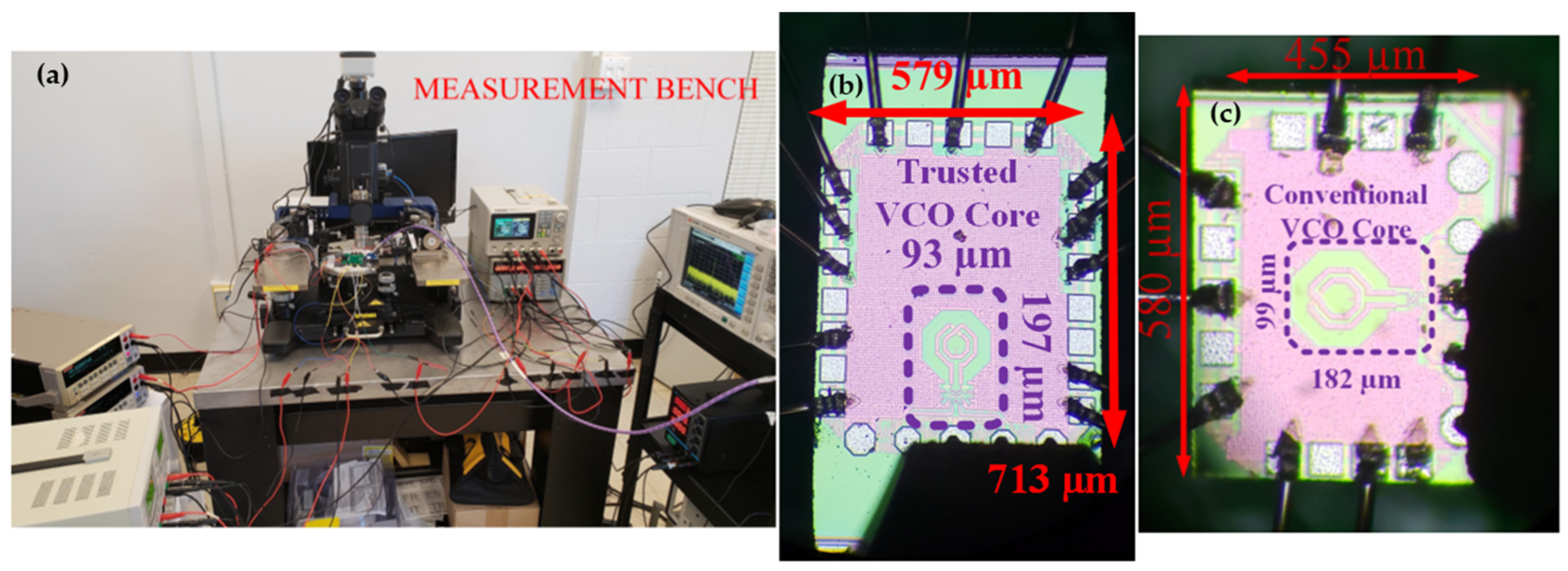
The proposed trusted VCO is implemented in a 1P9M 65 nm standard CMOS process (Figure 8b) and uses an on-chip open-drain NMOS buffer to interface with the measurement equipment (Figure 8a). A CVCO is also included on the same die for performance comparison (Figure 8c). To enable accurate performance measurement, both mm-Wave VCOs are characterized using RF GSG probes with external bias-Ts facilitating the connection to the power supply (Figure 8a). This way, the loss associated with external components (such as the cables) can be de-embedded from the measurement results. A general view of the test setup is shown in Figure 8a. While the core of both VCOs occupies a similar area (93 µm × 197 µm for the trusted VCO and 99 µm × 182 µm for CVCO), the trusted VCO needs additional pads to interface with the embedded PUF, resulting in a larger chip area. A Keysight PXA N9030A signal analyzer and several Keithley 2000 DMM source meters are used for the frequency analysis and DC characterization of the VCOs. The characterization process is split into two parts: VCO performance measurement and comparison and PUF characterization, randomness, and reliability analysis.

Figure 8.
Intra-HD micrographs of the (a) proposed trusted VCO and (b) CVCO dies alongside (c) the measurement bench.
4.1. VCO Performance Measurement and Comparison
Both VCOs are interfaced with the signal analyzer to monitor their output spectrum, measure their PN, and determine their TR. In this work, the proposed trusted VCO is designed for low-power applications; as such, the PUF is disabled during normal operation.
The trusted VCO sustains oscillation when the supply voltage (VDD) is raised to 0.8 V with the power consumption (PDC)~0.72 mW. For PDC~1.75 mW, the output power is increased to −9.7 dBm and the VCO exhibits a TR ≈ 5.5 GHz (Figure 9a), from ≈24.6 GHz to 30.1 GHz. Under such conditions, the PN measures better than −104.8 dBc/Hz and −132.2 dBc/Hz at 1 MHz and 10 MHz offset, respectively (Figure 9b), when the frequency is tuned to the upper end of the range (≈29.3 GHz). These results correspond to FoM~191.7 dBc/Hz and ~199.1 dBc/Hz @1MHz and @10MHz, respectively. When TR is considered, the FoMT of ~197.6 dBc/Hz and ~205 dBc/Hz are obtained at 1 MHz and 10 MHz, respectively. On the other hand, the CVCO sustains oscillation when the supply voltage (VDD) is raised to 0.8 V with the power consumption (PDC)~0.6 mW. For PDC~1.5 mW; the output power is increased to −10.1 dBm, and it exhibits a frequency tuning range (TR) of ≈6.1 GHz, from ≈25 GHz to 31.1 GHz (Figure 9a). Under such conditions, the PN measures better than −101.1 dBc/Hz and −130.4 dBc/Hz at 1 MHz and 10 MHz offset, respectively (Figure 9b), when the frequency is tuned to the upper end of the range (≈29.6 GHz). The CVCO PN results correspond to FoM~188.7 dBc/Hz and ~198 dBc/Hz @ 1 MHz and @ 10 MHz, respectively. When TR is considered, the FoMT of ~194.7 dBc/Hz and ~204 dBc/Hz are obtained at 1 MHz and 10 MHz, respectively. These results clearly show that the proposed trusted VCO exhibits similar performance (esp. PN), if not better, when compared against the CVCO under a similar power consumption.
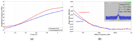
Figure 9.
(a) TR and (b) PN comparison of the trusted VCO with the CVCO. The spectrum of the trusted VCO is also shown.
The deterioration in the TR of the proposed trusted VCO is due to the extra capacitance resulting from parasitics of additional cross-coupled pairs and additional metal wiring in the layout. However, the slight closed-in PN improvement (esp. foffset < 1 MHz) in the proposed trusted VCO compared to the CVCO requires a more detailed analysis.
A number of PN models have been developed for LC VCOs [21,22,23,24,25]. Among them, the time variant PN model developed by Hajimiri et al. [21] is more accurate in predicting the PN of LC oscillators, particularly in the 1/f3 and 1/f2 regions. Considering this time variant PN model [21], calculating the change in the Impulse Sensitivity Function (ISF), which is a periodic and dimensionless function, is necessary [21]. Since the ISF is periodic, it can be represented by Fourier coefficients as follows:
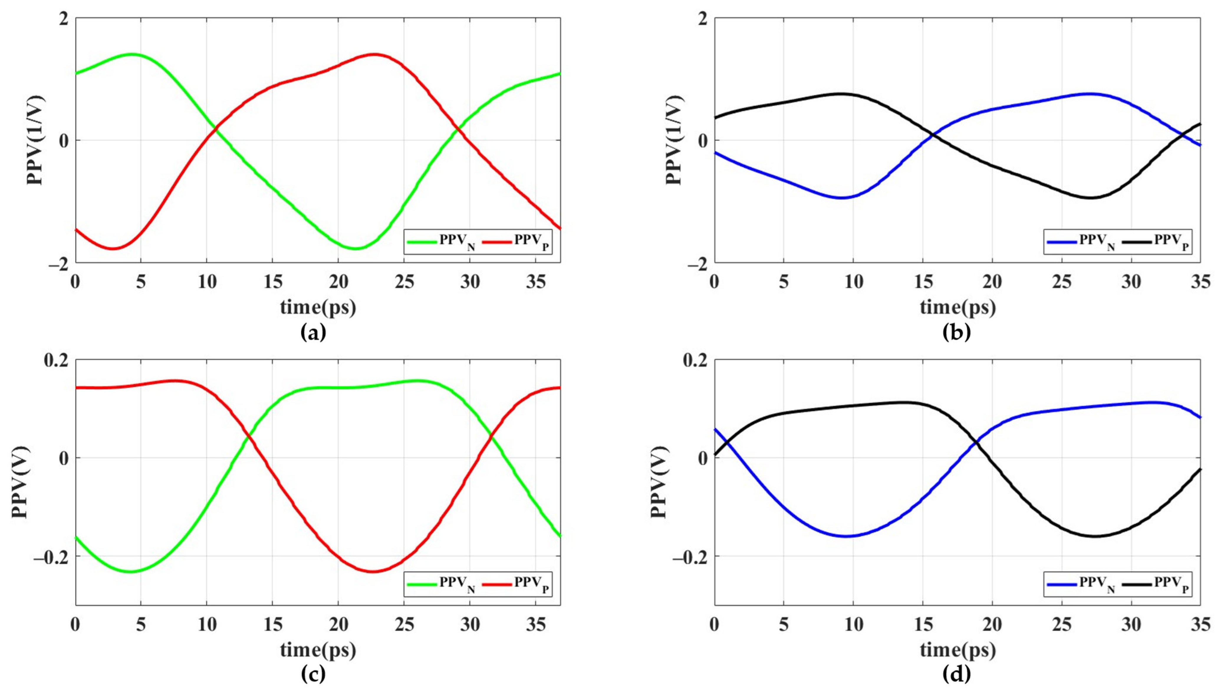
where the coefficients (Γn) are real values and θn is the phase of the nth harmonic. θn is small and can be ignored at random input noise [21], and the coefficients can be estimated analytically or calculated from the simulation. Given its similarities with the ISF, the Perturbation Projection Vector (PPV), which represents the sensitivity of the per cycle jitter variance to current perturbations at the nodes of the oscillator [23], can be used to estimate the ISF changes [21,22,23]. PPV results can be obtained via periodic simulations. Figure 10 gives the PPV results obtained from Cadence Harmonic Balance (HB) and HB noise simulations for both VCOs. HB PPV results are shown in V and HB noise PPV results are shown in 1/V. Then, the PN of the LC VCO can be expressed as follows [24,25]:
where qmax is the maximum charge displacement across the equivalent output capacitance where the impulse was injected, i.e., qmax = VmaxC (Vmax is the maximum voltage swing at the output). is the ISF from active devices and can be expressed in several forms, e.g., [24] or [25], where β = µeCoxW/L, µe is the electron mobility, Cox the gate oxide capacitance per unit area, and W and L are the transistor width and length, respectively. is the ISF from the thermal noise source of the oscillator (R), which is mostly produced by the tank. It is assumed to be 1/2 for single-ended output and 1/8 for differential outputs [25]. is the power spectral density of active devices’ noise current. The portion associated with the thermal noise can be expressed as , where k is the Boltzmann constant, is the fitting parameter, and T is the temperature as Kelvin. In most cases, of the device. The portion associated with the flicker noise can be expressed as , where is the flicker noise fitting parameter. is the power spectral density of the thermal noise current due to R and can be expressed as . Equation (6) includes the thermal and flicker noise sources [19,21,22,23,24,25,26,27,28,29,30] for both active and passive devices in the VCO. Since the flicker and thermal noises of MOS devices are considered uncorrelated, their impact on the PN can be studied separately, and the results can be superimposed [22]. Knowing that flicker noise is dominant at low offset frequencies, the impact of the flicker noise on the PN should be studied in more detail. Hajimiri et al. [21] expresses the flicker noise-dominant region of the PN (i.e., 1/f3 region) in terms of the 1/f noise corner, ω1/f. In this case, the 1/f3 corner frequency, , can be expressed as follows:
where is 1/f3 corner frequency, is 1/f corner frequency, and and are DC and root mean square (RMS) values of the ISF coefficients, respectively. Using (7), the flicker noise-dominant portion of the PN can be expressed as follows:
where is the first coefficient of the ISF, and is equal to 2ΓDC, and is the total noise current, . At low offset frequencies, the flicker noise will be dominant; hence, can be expressed as . Knowing the flicker and thermal noise of the MOS devices and the tank, the flicker noise- and thermal noise-dominant portions of the PN can be derived separately as follows [31,32,33]:
where IDD is the RMS current consumption of the VCO. Superimposing (9) to (10) leads to a simplified PN expression that covers both the flicker noise- and thermal noise-dominant regions of the PN as follows:

Figure 10.
PPV results: HB noise results for (a) the CVCO and (b) trusted VCO; HB results for (c) the CVCO and (d) trusted VCO.
The PN for two LC VCOs can then be compared using this simplified PN expression. PPV results for both designs are gathered and compared. Γ0 obtained from the HB noise simulation is 1.085 1/V and −1.44 1/V for the differential outputs of the CVCO and 0.36 1/V and −0.19 1/V for the differential outputs of the trusted VCO, respectively (Figure 10). Utilizing HB simulations reveals Γ0~−0.16 V and 0.14 V for the differential outputs of the CVCO and ~0.0049 V and 0.058 V for the differential outputs of the trusted VCO, respectively (Figure 10). The minimum ratio between Γ0 for two VCOs is ~2.4×, which amounts to a ~7 dB improvement in the close-in PN for the trusted VCO. Additionally, the trusted VCO exhibits larger qmax compared to the CVCO due to larger parasitic capacitors from the additional cross-coupled pairs and the resulting on-chip metal wiring. This larger qmax further improves the close-in PN performance of the proposed trusted VCO. The measured PN results presented in Figure 9 reveal up to a 9 dB improvement in the PN at 100 kHz offset for the trusted VCO compared to the CVCO. As the frequency increases, the effect of flicker noise diminishes, and the thermal noise of active devices and the Q of the LC tank become the dominant factor affecting the PN [18]. In this region, the PN can be better modeled with (11). Considering (11), it is evident that the difference between the PN of two VCOs gradually narrows until it becomes negligible at high offset frequencies near the PN floor. To conclude this study, the performance of the trusted VCO is summarized and presented in Table 1. Compared with the state-of-the-art VCOs [26,27,28,29] operating in a similar frequency range and built with the 65 nm CMOS process, the proposed trusted VCO exhibits competitive FoMs while consuming lower power.

Table 1.
Trusted VCO performance summary and comparison with state-of-the-art VCOs.
4.2. PUF Characterization and Randomness Analysis
To characterize a PUF, the randomness, uniqueness, and correlation criteria should be evaluated. For conventional PUFs, the direct analysis of the response is sufficient. However, the proposed embedded PUF requires customized digitization since each challenge will generate multiple responses. As the first step, the expected PDF of the responses is presented to quantify the reliability of the PUF [5]. Figure 11 shows the distribution of the measured current consumption and fosc for a trusted VCO chip operating under VDD = 1.2 V at room temperature (27 °C). Since the current consumption and fosc are directly affected by the device size, which follows the near-Gaussian mismatch profile of CMOS devices, a normal distribution is expected. To perform HD analysis, the measured current consumption and fosc should be converted to binary strings. The conversion is customized considering the accuracy of the measurement equipment and biasing (which sets the minimum resolution) and the variation range of the measured parameters (current consumption and fosc). In this work, measurement devices have 1 MHz and 1 µA accuracy. However, the accuracy of biasing voltage sources used for the challenge pairs is ~10 mV and, hence, sets the minimum resolution for the responses. During the authentication, each challenge input based on the “CN3 CN2 CN1 CP3 CP2 CP1” codeword produces its own unique response as current consumption and fosc. Knowing that the length of the output bit string should be equal to or greater than that of the challenge codeword [20], a lower bound (six bits) on the length of the bit string is found. However, accurate conversion of the output analog response to bit strings is a challenge for this work since multiple outputs are generated for each challenge input. Unlike most analog PUFs [10,11,12,13,14,15], setting a fixed decision threshold is difficult for all chips given normal PVT variations affecting the high-frequency path. As such, the soft decision technique [12] is used for output bit string generation before the HD analysis.
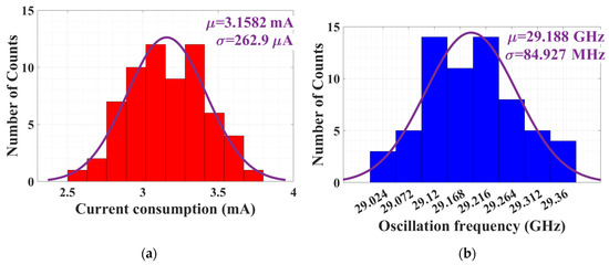
Figure 11.
PDF of the (a) current consumption and (b) fosc for the 6-bit input challenge.
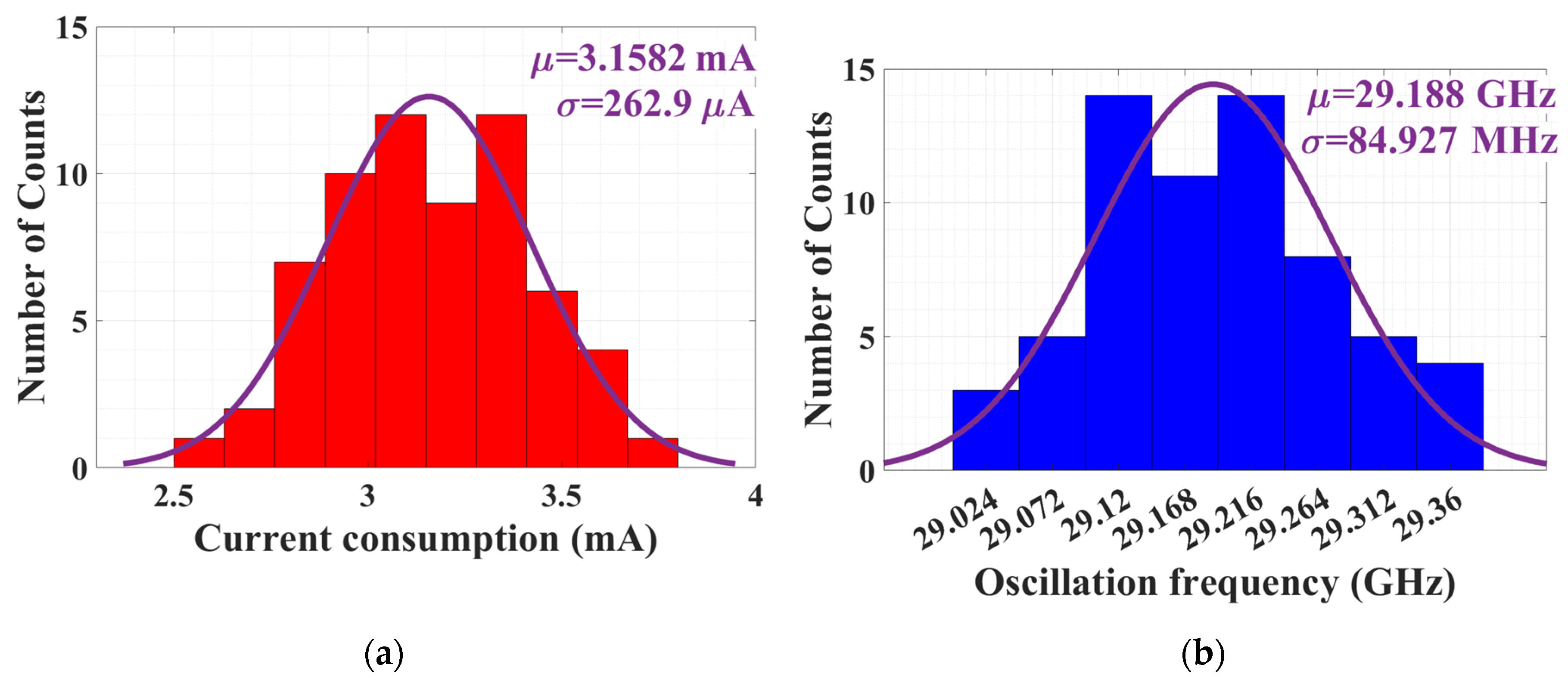
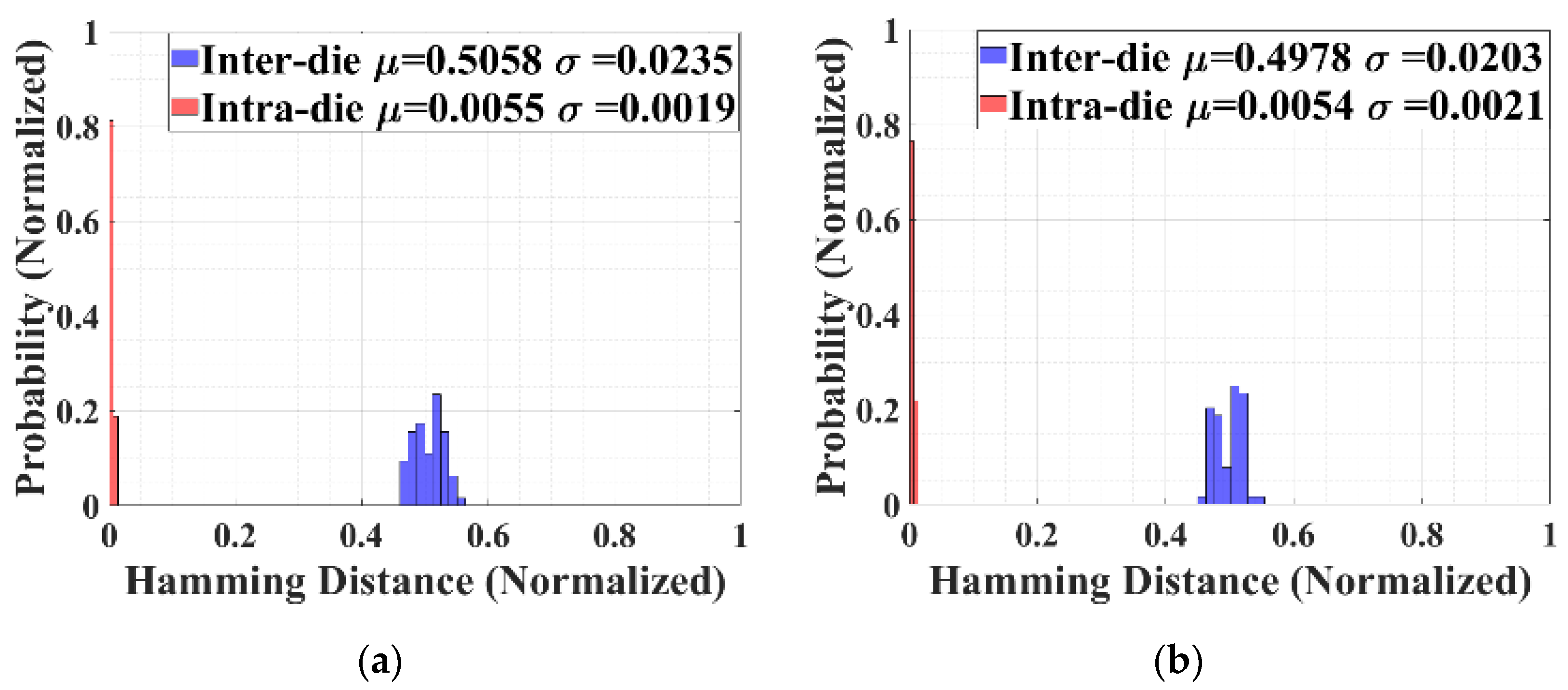
First, the responses are analyzed to find the variation range. When the input challenge moves from 000000 to 111111, the current consumption (i.e., the DC response) changes from ~2.6 mA to ~3.8 mA, and fosc (i.e., the AC response) varies from ~29 GHz to ~29.4 GHz, respectively. Then, the weight of each digit in the decimal number is considered. Knowing the accuracy of the measurement equipment, both current (in mA) and fosc (in GHz) readings can be expressed with three decimal digit accuracy, i.e., A.XYZ for current and BC.TVU for frequency. A level change for the current response can be 2 or 3, other level changes can be from 0 to 9, indicating that the changes have an unequal impact on the response. In such conditions, coding theory approaches, such as Huffman coding [20], where higher probability represents fewer bits and vice versa, are desired. Due to the limited accuracy of the biasing network (~10 mV), the least significant digits, i.e., Z and U, require soft decision thresholds. Finally, the proposed customized coding can be expressed as 1-bit for A, 4-bit for X, 4-bit for Y, 1-bit for Z, 1-bit for B, 1-bit for C, 3-bit for T, 4-bit for V, and 1-bit for U. The result will be two 10-bit codewords, one for the current consumption response and the other for fosc. Using this customized code, a sample set consisting of eight dies operating under similar conditions (VDD = 1.2 V and T ≈ 27 °C) is evaluated for Inter-HD and Intra-HD analyses (Figure 12). The measured average Inter-HD of the current consumption and fosc are ~0.5058b and 0.4978b, respectively, which are very close to the ideal value of 0.5b. Similarly, the measured average Intra-HD of the current consumption and fosc are 0.0055b and 0.0053b, respectively, which are very close to the ideal value of 0, demonstrating acceptable randomness for the proposed analog embedded PUF.
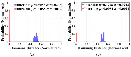
Figure 12.
Measured Intra- and Inter-HD of the (a) current consumption (a) and (b) fosc of the trusted VCO for eight dies.
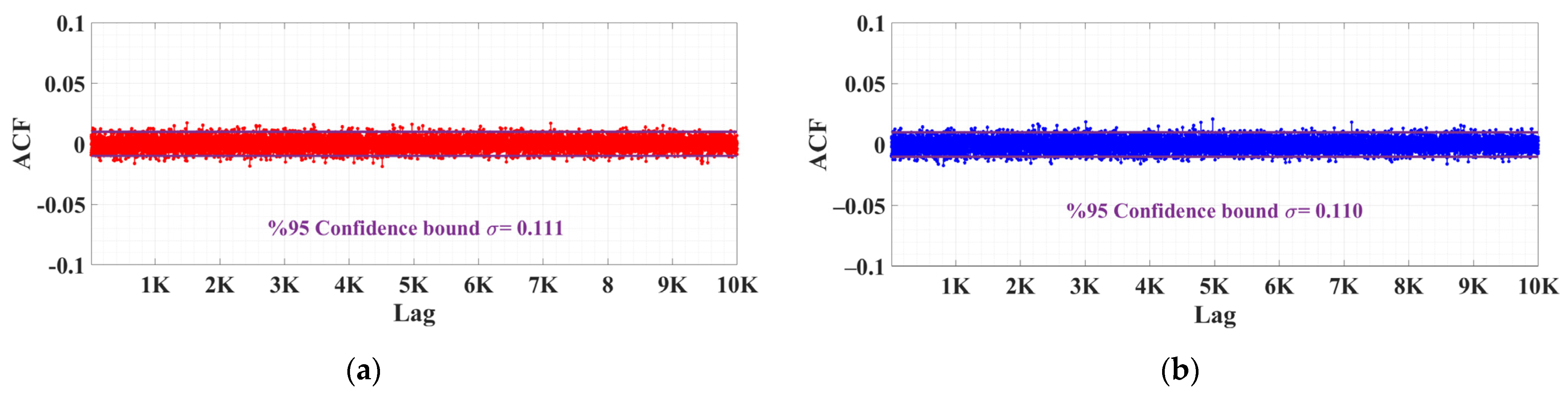
To quantify the degree of correlation between the PUF outputs for different challenges, the ACF of the proposed analog PUF is evaluated [34]. ACF measures the correlation of a signal with a delayed copy of itself as a function of delay. The smaller the value of the correlation is, the lower the correlation of the responses and the higher the resemblance to the Gaussian distribution. For conventional PUFs, bit streams of responses are used for ACF measurements. In this work, the ACF is applied to current consumption and fosc, which make up the output responses to each challenge. To compute ACF, a stochastic time series of measured responses is created since the ACF aims to detect the correlation between two random responses in a sample set. To this end, 40K responses are gathered for each output to create the required stochastic time series for the eight chips. Then, the ACF of both 40K sample sets, one for current consumption and the other for fosc, is calculated when considering 10K lags (Figure 13). The ACF of the responses for the current consumption and fosc at a 95% confidence level are 0.0111 and 0.0110, respectively, which are very close to the ideal value of zero, demonstrating a desired level of randomness for the proposed PUF (Table 2).

Figure 13.
Autocorrelation of the 40K sample set with 10K lags: (a) current consumption, (b) fosc responses.
Table 2.
PUF performance summary and comparison with state-of-the-art analog PUFs.
The performance of the proposed embedded analog PUF is summarized in Table 2 and compared against those of the published state-of-the-art analog PUFs. The proposed analog-embedded PUF offers a competitive performance in terms of entropy, energy consumption, and bit rate while occupying a smaller chip area in a similar 65 nm CMOS process. An important advantage of the proposed analog PUF is its high sampling rate. The sampling rate is calculated by simulating the settling time of the VCO when switching the input challenge bit (Figure 14). As shown in Figure 14, the VCO frequency changes and settles to the new frequency within ~4 ns when switching from the first to the last challenge, enabling a bit rate as high as 1.5 Gbps for each response type due to the 6-bit length of the challenge. The bit rate is calculated by multiplication of the sampling rate (Nyquist criterion) and the number of bits for each symbol, which is the length of challenges in this work [35] as shown below:
where is the number of bits for each symbol (i.e., six bits for the proposed PUF), is the sampling rate, and tsettling is the slowest settling time from the first challenge to the last challenge (i.e., ~4 ns for the proposed PUF). Such a high data rate allows for reducing the time needed for the authentication process and reducing the unwanted latency when trying to establish a trusted data link. Using (12), the energy per bit can be calculated by subtracting the VCO power during the authentication with the one during the normal operation (i.e., challenge set to 000000), revealing a competitive performance compared to the state-of-the-art (Table 2). The very high data rate achieved for the proposed embedded PUG along with its low power consumption allows for delivering an energy/bit as low as 0.83 pJ, which is comparable to the state-of-the-art PUFs [12,14,15] implemented in a similar CMOS technology. Moreover, the larger CRP size made available by the generation of multiple outputs for a single challenge has created a relatively compact design compared to other analog PUFs implemented in similar CMOS process nodes, making the design well-suited for integration with communication transceivers.
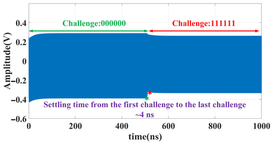
Figure 14.
Transient simulation results of the trusted VCO showing the settling time when input challenge changes criterion and the number of bits for each symbol.
5. Conclusions
An innovative 1.75 mW trusted CMOS LC VCO, which employs an embedded analog PUF and operates at 24.6 GHz to 30.1 GHz, is presented. The VCO benefits from an analog PUF, which is integrated within the cross-coupled CMOS pair, allowing for a larger set of CRPs with the same number of input challenges. Fabricated in a 1P9M 65 nm standard CMOS process, the proposed trusted VCO delivers the measured PN ~−104.8 dBc/Hz @ 1 MHz and −132.2 dBc/Hz @ 10 MHz, revealing FoMs of 191.7 dBc/Hz and 199.1 dBc/Hz, respectively. With TR~5.5 GHz, the FoMT reaches 197.6 dBc/Hz and 205.0 dBc/Hz @ 1 MHz and @ 10 MHz, respectively. The embedded PUF consumes as low as 0.83 pJ/b and is capable of running at 1.5 Gb/s. It exhibits sufficient uniqueness with the measured Inter-HD of 0.5113b and 0.489b and measured Intra-HD of 0.0055b and 0.0053b for the current consumption and fosc, respectively. Moreover, an ACF of 0.0111 and 0.110 is achieved for the current consumption and fosc responses of the proposed PUF, respectively, at a 95% confidence level. Compared with the state-of-the-art LC VCOs operating in the same frequency range, the proposed trusted VCO shows competitive performance at lower power with added device security and authentication features.
Author Contributions
Conceptualization, A.K. and H.M.L.; investigation, A.K. and H.M.L.; methodology, A.K. and H.M.L.; software, A.K.; supervision, H.M.L. and S.M.; visualization, A.K.; writing—original draft, A.K., H.M.L., A.H.M.S. and S.M.; writing—review & editing, A.K., H.M.L., A.H.M.S. and S.M. All authors have read and agreed to the published version of the manuscript.
Funding
The research received no external funding.
Data Availability Statement
All the materials used in the study are mentioned within the article.
Conflicts of Interest
The authors declare no conflicts of interest.
References
- Agiwal, M.; Roy, A.; Saxena, N. Next Generation 5G Wireless Networks: A Comprehensive Survey. IEEE Commun. Surv. Tutor. 2016, 18, 1617–1655. [Google Scholar] [CrossRef]
- Sanabria-Borbón, A.C.; Jayasankaran, N.G.; Hu, J.; Rajendran, J.; Sánchez-Sinencio, E. Analog/RF IP Protection: Attack Models, Defense Techniques, and Challenges. IEEE Trans. Circuits Syst. II-Express Briefs 2021, 68, 36–41. [Google Scholar] [CrossRef]
- Rizo, A.R.D.; Leonhard, J.; Aboushady, H.; Stratigopoulos, H.-G. RF Transceiver Security against Piracy Attacks. IEEE Trans. Circuits Syst. II-Express Briefs 2022, 69, 3169–3173. [Google Scholar] [CrossRef]
- Skorobogatov, S. Semi-Invasive Attacks—A New Approach to Hardware Security Analysis; Technical Report; University of Cambridge, Computer Laboratory: London, UK, 2005. [Google Scholar]
- Tehranipoor, M.; Wang, C. Introduction to Hardware Security and Trust; Springer Science & Business Media: Berlin/Heidelberg, Germany, 2012. [Google Scholar] [CrossRef]
- Elshamy, M.; Di Natale, G.; Sayed, A.; Pavlidis, A.; Louërat, M.-M.; Aboushady, H.; Stratigopoulos, H.-G. Digital-to-Analog Hardware Trojan Attacks. IEEE Trans. Circuits Syst. I-Regul. Pap. 2022, 69, 573–586. [Google Scholar] [CrossRef]
- Skorobogatov, S. Side-Channel Attacks: New Directions and Horizons; ECRYPT2 School on Design and Security of Cryptograph-ic Algorithms and Devices: Albena, Bulgaria, 2011; Volume 29. [Google Scholar]
- Zoni, D. Analysis and Countermeasures to Side-Channel Attacks: A Hardware Design Perspective. In Proceedings of the 2019 14th International Symposium on Reconfigurable Communication-Centric Systems-on-Chip (ReCoSoC), New York, NY, USA, 1–3 July 2019; pp. 1–4. [Google Scholar]
- Leonhard, J.; Sayed, A.; Louërat, M.-M.; Aboushady, H.; Stratigopoulos, H.-G. Analog and Mixed-Signal IC Security via Sizing Camouflaging. IEEE Trans. Comput.-Aided Des. Integr. Circuits Syst. 2021, 40, 822–835. [Google Scholar] [CrossRef]
- Scholz, A.; Zimmermann, L.; Sikora, A.; Tahoori, M.B.; Aghassi-Hagmann, J. Embedded Analog Physical Unclonable Function System to Extract Reliable and Unique Security Keys. Appl. Sci. 2020, 10, 759. [Google Scholar] [CrossRef]
- Zimmermann, L.; Scholz, A.; Tahoori, M.B.; Aghassi-Hagmann, J.; Sikora, A. Design and Evaluation of a Printed Analog-Based Differential Physical Unclonable Function. IEEE Trans. Very Large Scale Integr. Syst. 2019, 27, 2498–2510. [Google Scholar] [CrossRef]
- Tang, Q.; Choi, W.H.; Everson, L.; Parhi, K.K.; Kim, C.H. A Physical Unclonable Function Based on Capacitor Mismatch in a Charge-Redistribution SAR-ADC. In Proceedings of the 2018 IEEE International Symposium on Circuits and Systems (IS-CAS), Florence, Italy, 27–30 May 2018; pp. 1–5. [Google Scholar]
- Danesh, M.; Venkatasubramaniyan, A.B.; Kapoor, G.; Sanyal, A. A 0.36pJ/Bit Analog PUF Based on Current Steering DAC and VCO. In Proceedings of the 2019 IEEE 62nd International Midwest Symposium on Circuits and Systems (MWSCAS), Dallas, TX, USA, 4–7 August 2019; pp. 578–581. [Google Scholar]
- Asghari, M.; Guzman, M.; Maghari, N. Cross-Coupled Impedance-Based Physically Unclonable Function (PUF) with 1.06% Native Instability. IEEE Solid-State Circuits Lett. 2020, 3, 282–285. [Google Scholar] [CrossRef]
- Zhang, J.; Ding, L.; Chen, Z.; Li, W.; Qu, G. DA PUF. In Proceedings of the 59th ACM/IEEE Design Automation Conference, New York, NY, USA, 10–14 July 2022. [Google Scholar] [CrossRef]
- Yuvaraja, S.A.; Khandelwal, V.; Tang, X.; Li, X. Wide Bandgap Semiconductor-Based Integrated Circuits. Chip 2023, 2, 100072. [Google Scholar] [CrossRef]
- Ham, D.A.; Hajimiri, A. Concepts and Methods in Optimization of Integrated LC VCOs. IEEE J. Solid-State Circuits 2001, 36, 896–909. [Google Scholar] [CrossRef]
- Tiebout, M. Low Power VCO Design in CMOS; Springer Science and Business Media: Boston, MA, USA, 2005. [Google Scholar]
- Yang, H.Y.D. Design Considerations, of Differential Inductors in CMOS Technology for RFIC. In Proceedings of the 2004 IEEE Radio Frequency Integrated Circuits (RFIC) Systems. Digest of Papers, Forth Worth, TX, USA, 6–8 June 2004; pp. 449–452. [Google Scholar]
- Cover, T.M.; Thomas, J.A. Elements of Information Theory; Wiley: Hoboken, NJ, USA, 2001. [Google Scholar] [CrossRef]
- Hajimiri, A.; Lee, T.H. A General Theory of Phase Noise in Electrical Oscillators. IEEE J. Solid-State Circuits 1998, 33, 179–194. [Google Scholar] [CrossRef]
- Mukherjee, J.; Roblin, P.; Akhtar, S. An Analytic Circuit-Based Model for White and Flicker Phase Noise in LC Oscillators. IEEE Trans. Circuits Syst. 2007, 54, 1584–1598. [Google Scholar] [CrossRef]
- Demir, A.; Roychowdhury, J. A Reliable and Efficient Procedure for Oscillator PPV Computation, with Phase Noise Macromodeling Applications. IEEE Trans. Comput.-Aided Des. Integr. Circuits Syst. 2003, 22, 188–197. [Google Scholar] [CrossRef]
- Wu, X.; Xu, T.; Meng, J.; Chen, J. Analysis of Phase Noise Model in Cross-Coupled LC VCO. Chin. J. Electron. 2012, 21, 379–383. [Google Scholar]
- Andreani, P.; Wang, X.; Vandi, L.; Fard, A. A Study of Phase Noise in Colpitts and LC-Tank CMOS Oscillators. IEEE J. Solid-State Circuits 2005, 40, 1107–1118. [Google Scholar] [CrossRef]
- Masnadi, A.; Mahani, M.; Lavasani, H.M.; Mirabbasi, S.; Shekhar, S.; Zavari, R.; Djahanshahi, H. A Compact Dual-Core 26.1-to-29.9GHz Coupled-CMOS LC-VCO with Implicit Common-Mode Resonance and FoM of-191 dBc/Hz at 10MHz. In Proceedings of the 2020 IEEE Custom Integrated Circuits Conference (CICC), Boston, MA, USA, 22–25 March 2020; pp. 1–4. [Google Scholar]
- Guo, H.; Chen, Y.; Mak, P.-I.; Martins, R.P. 26.2 A 0.08mm2 25.5-to-29.9GHz Multi-Resonant-RLCM-Tank VCO Using a Sin-gle-Turn Multi-Tap Inductor and CM-Only Capacitors Achieving 191.6dBc/Hz FoM and 130kHz 1/F3 PN Corner. In Proceedings of the 2019 IEEE International Solid-State Circuits Conference—(ISSCC), San Francisco, CA, USA, 17–21 February 2019; pp. 410–412. [Google Scholar]
- Hossain, A.; Lee, S.B.; Byeon, C.W. 30-GHz Low-Phase-Noise VCO With Negative Transconductance Optimization in 65-Nm CMOS. IEEE Microw. Wirel. Technol. Lett. 2023, 33, 59–62. [Google Scholar] [CrossRef]
- Cho, Y.; Nam, J.-W.; Lee, S. A Low-Power Class-C Voltage-Controlled Oscillator with Robust Start-Up and Compact High-Q Capacitor Array. IEEE Trans. Circuits Syst. II-Express Briefs 2022, 69, 819–823. [Google Scholar] [CrossRef]
- Hu, Y.A.; Siriburanon, T.; Staszewski, R.B. Oscillator Flicker Phase Noise: A Tutorial. IEEE Trans. Circuits Syst. II-Express Briefs 2021, 68, 538–544. [Google Scholar] [CrossRef]
- Lee, T.H.; Hajimiri, A. Oscillator Phase Noise: A Tutorial. IEEE J. Solid-State Circuits 2000, 35, 326–336. [Google Scholar] [CrossRef]
- Razavi, B. The Design of a Millimeter-Wave VCO [The Analog Mind]. IEEE Solid-State Circuits Mag. 2022, 14, 6–12. [Google Scholar] [CrossRef]
- Wang, H.; Hajimiri, A.; Lee, T.H. Comments on “Design Issues in CMOS Differential LC Oscillators” [and Reply]. IEEE J. Solid-State Circuits 2000, 35, 286–287. [Google Scholar] [CrossRef]
- Li, G.A.; Wang, P.; Ma, X.; Shi, Y.; Chen, B.; Zhang, Y. A Multimode Configurable Physically Unclonable Function with Bit-Instability-Screening and Power-Gating Strategies. IEEE Trans. Very Large Scale Integr. Syst. 2021, 29, 100–111. [Google Scholar] [CrossRef]
- Proakis, J.G. Digital Communications. In Routledge eBooks; McGraw-Hill: New York, NY, USA, 2007; pp. 207–212. [Google Scholar] [CrossRef]


Disclaimer/Publisher’s Note: The statements, opinions and data contained in all publications are solely those of the individual author(s) and contributor(s) and not of MDPI and/or the editor(s). MDPI and/or the editor(s) disclaim responsibility for any injury to people or property resulting from any ideas, methods, instructions or products referred to in the content. |
© 2024 by the authors. Licensee MDPI, Basel, Switzerland. This article is an open access article distributed under the terms and conditions of the Creative Commons Attribution (CC BY) license (https://creativecommons.org/licenses/by/4.0/).