Abstract
In this paper, a novel kind of mode composite transmission line (MC-TL) is proposed, and a dual-band power divider with a large frequency ratio using this novel MC-TL for 5G communication systems was developed. The proposed MC-TL was developed using spoof surface plasmon polaritons (SSPPs) and a corrugated substrate-integrated waveguide (CSIW) transmission line, which supports both a surface plasmon mode and TE10 mode, independently. The surface plasmon mode operates in the grooves of the surface metal layer, while the TE10 mode works in the substrate between two metal layers. These two parts can transmit different modes at independent frequencies. This structure can be used in dual-band transmission lines with a high frequency ratio. The characteristics and design of the MC-TL (SSPPs and CSIW) are analyzed and illustrated. The MC-TL was fabricated and measured to demonstrate its performance. Moreover, based on the proposed MC-TL, a dual-band power divider with a large frequency ratio (operating at 3 GHz and 28 GHz simultaneously) was also designed and fabricated. It can cover the frequency of a fifth-generation communication system perfectly. The measured outcomes align closely with the simulated results, demonstrating robust agreement and showcasing excellent transmission capabilities.
1. Introduction
Modern developments in 5G wireless communication systems require highly integrated, geometrically compact radio frequencies, microwave circuits, and modules featuring broadband and multi-band functionalities. The most widely used frequency bands for commercial wireless communications such as mobile phones and wireless Internet connectivity are allocated in the low microwave frequency ranges of up to 6.0 GHz [1], covering popular bands of 900 MHz, 1.9 GHz, 2.45 GHz, 3.5 GHz, and 5.8 GHz. Within the advancing realm of fifth-generation (5G) wireless communication networks, operational frequencies may extend to 28 GHz, 35 GHz, and even up to 57–71 GHz [2]. Consequently, a significant disparity in frequency arises between existing and upcoming wireless communication infrastructures. In recent years, many high-performance dual-band power dividers, filters, and antennas have been developed as key components of RF systems [3,4], but a very large frequency ratio is difficult to use, so the frequency ratio of most research results has been less than 3, which does not meet the requirements of a 5G system.
In acknowledging the noted apprehensions, an innovative mode composite waveguide (MCW) was introduced and validated in [5]. This structure integrates an inner rectangular metallic core with an outer rectangular metallic sheath. Over the past few years, substrate-integrated waveguides (SIWs) have garnered considerable attention due to their compactness and minimal signal loss [6]. An interior conductor functions as an SIW, facilitating the transmission of high-frequency signals, while the external enclosure and the surrounding surface of the inner conductor collectively serve as a substrate-integrated coaxial line, supporting a TEM mode at low frequencies. A dual-band antenna has been implemented to support 5.8 and 30 GHz simultaneously by integrating an annular-ring antenna element and SIW slot antenna element [7]. This structure uses two layers of substrate and uses slots to couple energy from the SIW to a microstrip line. The ports are in the form of microstrip lines.
Nevertheless, in the current MCW configuration, the complexity remains high due to the multilayer PCB process, making integration with other planar circuits arduous and impeding the utilization of the SIW segment for antenna designs. Thus, researchers are compelled to devise a single-layer planar transmission line to expose the SIW to the surrounding air. Consequently, a fresh composite transmission line, dubbed the dual-mode composite microstrip line (DMCMS), has been introduced, merging an SIW with a microstrip line and designating the SIW as the thick conductor strip within the microstrip line [7]. An SIW and CPW have also been combined as a new transmission line. While the SIW has a cutoff frequency, the bandwidth of the coplanar waveguide transmission covers both low and high frequencies. This feature can meet the requirements of a high frequency ratio [8].
The utilization of substrate-integrated waveguide (SIW) technology represents a highly favorable strategy in the creation of transmission structures within a high-frequency microwave circuit design, owing to its minimal losses, straightforward architecture, and seamless compatibility with additional planar circuits. As a structure for microwave transmission on onboard media, SIWs are widely used in communication, radar, satellite communication, microwave sensor, and RFID and RF front-end design applications. A wide range of low-cost and high-performance SIW circuits and antennas have been developed [9,10,11,12,13].
SIWs can also be combined with spoof surface plasmon polaritons (SSPPs). SSPPs are slow waves that propagate along the interface of an air–metal surface in the terahertz and microwave frequencies [14,15,16,17]. SSPPs are two-dimensional electromagnetic fields that are highly localized, propagate along metal–dielectric interfaces, and decay exponentially into adjacent media. Owing to the advantages of confined electromagnetic fields in subwavelength scales, SSPPs have some potential applications.
In [18], SSPPs and SIWs were used as two different frequency input terminals of an antenna. With the good isolation of SSPPs and an SIW, two transmission lines (TLs) can share the same antenna and can obtain a result that the frequencies do not interfere with each other. Recently, there have been many studies that combine SSPPs and an SIW into a filter, since SIWs have high-frequency passing characteristics, and SSPPs have low-frequency passing characteristics. However, all these structures [19,20,21] have SSPPs inside the SIW, and obtained only bandpass filters.
SIW substrate metallization vias direct current from the upper surface conductor to the lower surface conductor, and it is not appropriate to place SSPP structures on both sides of the SIW. The corrugated SIW (CSIW) [22], as a member of the SIW family, has a similar physical structure to that of SSPPs. A CSIW achieves TE10-type boundary conditions by replacing vias with quarter-wavelength microstrip stubs arranged in ripples at the waveguide edges. The CSIW changes the structure of the metallized vias so that the SSPP structure is integrated on both sides of the top surface conductor. For these reasons, a single-layer mode composite transmission line is proposed in this paper that combines SSPPs with a CSIW.
In this paper, Section 2 introduces and discusses the principles of Hybrid SSPPs and the CSIW structure. Section 3 provides the MC-TL design. Section 4 discusses the simulation and measurement of the MC-TL, and the results are analyzed appropriately. In Section 5, a dual-band power divider based on the MC-TL is proposed, which can work in both low-frequency passbands and high-frequency passbands as a so-called dual-band power divider. Then, the measured results are presented, showing agreement with the simulation results.
2. Principle of Hybrid SSPPs and CSIW Structure
2.1. The Transition from SIW to CSIW
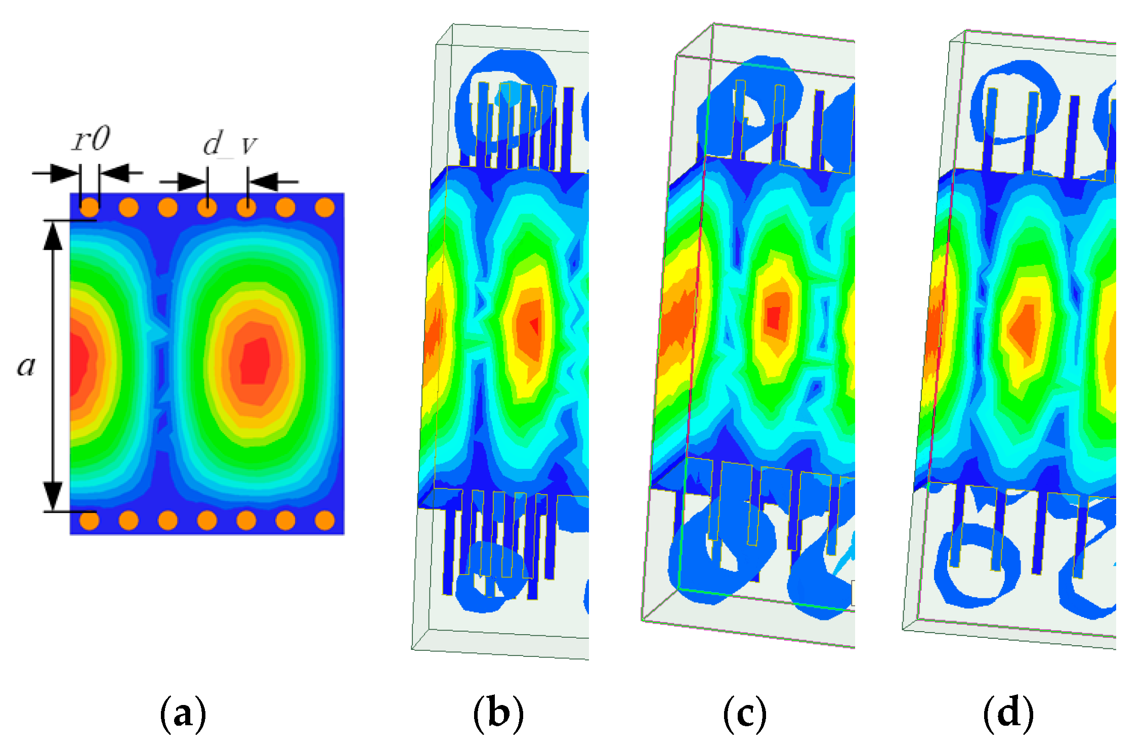
Figure 1 shows the electric field distribution of the substrate-integrated waveguide and the structure where the metallized through-holes are replaced with different forms of open stub lines, including a SIW TL, double-layer open-stub line substrate-integrated waveguide, double-layer open-stub line substrate-integrated waveguide with increased distance of each branch, and single-layer open-stub line substrate-integrated waveguide. They operate in TE10 or quasi-TE10 mode. As shown in Figure 1a, the SIW is composed of two rows of metallic via holes on the substrate, which can make the current flow from the upper surface of the dielectric substrate to the lower surface, where r0 is the diameter of the metallic via holes, and d_v is the hole spacing. The fundamental mode in the SIW is TE10 mode, and the dispersion relationship is [23]
where β is the propagation constant of the TE10 mode, ωs is the center distance of two metallized vias at relative positions on both sides of the dielectric substrate, and εr and μr are the relative permittivity and permeability.
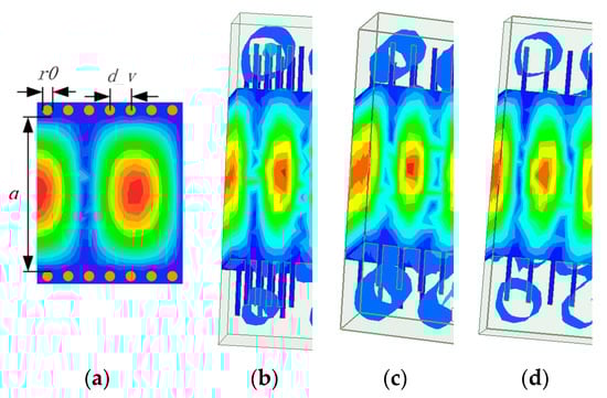
Figure 1.
Simulated E-field distribution. (a) SIW TL. (b) Double-layer open-stub line substrate-integrated waveguide. (c) Double-layer open-stub line substrate-integrated waveguide with increased distance of each branch. (d) Single-layer open-stub line substrate-integrated waveguide.
TE10 is limited to the inside of the SIW due to the metal columns connecting the top and bottom metal layers. When we consider the metallic via hole as a short path between the top and bottom metal layers, the hole can be replaced with a short segment that simultaneously opens on the upper and lower layers of the substrate, as shown in Figure 1b. In the so-called double-layer open-stub line substrate-integrated waveguide, the TE10 mode is still working in the substrate, between the top and bottom metal layers, which is the same place and mode as in the SIW. The TE10 mode is still working when changing the distance between the open-stub, as shown in Figure 1c. When the distance between adjacent open stubs becomes larger, the working mode of TE10 does not change. As shown in Figure 1d, when the bottom open stub is changed into ground metal, the working mode of TE10 does not change with it. It can be seen that the structure of the CSIW, which is changed from SIW, is similar to the structure of the SSPPs. In Figure 1, there is some electromagnetic energy at the end of the open stub, which is caused by the periodicity of the microwave circuit; it cannot be avoided, but it can be set outside the operating frequency.
2.2. Dispersion Analysis of SSPPs
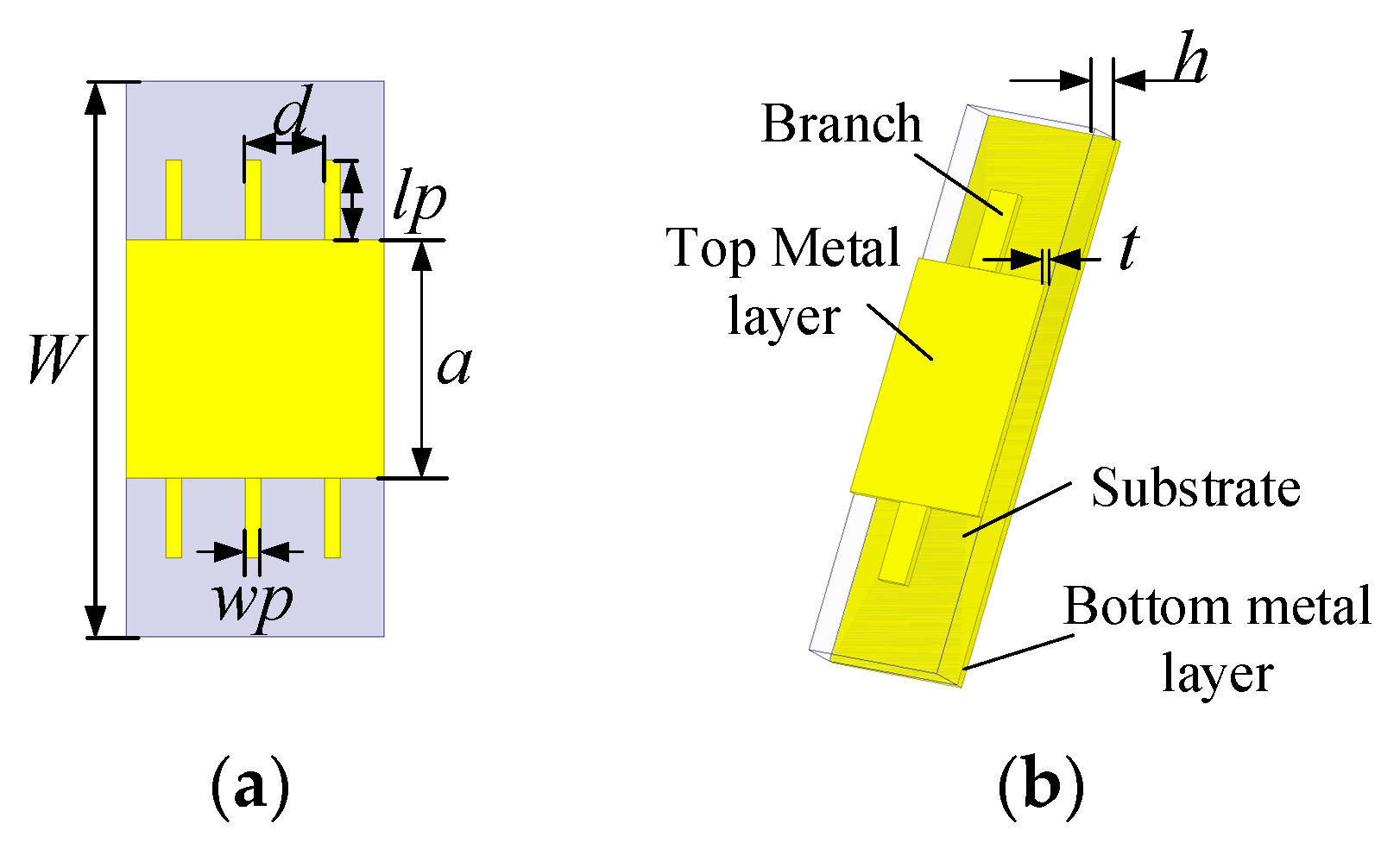
In investigating the characteristics of the multilayered composite transmission line (MC-TL) formed by merging spoof surface plasmon polaritons (SSPPs) and the composite substrate-integrated waveguide (CSIW), our initial focus is on analyzing the dispersion properties of the MC-TL unit cell. Figure 2 shows diagrams of the top-down views of the MC-TL and its individual unit cell.
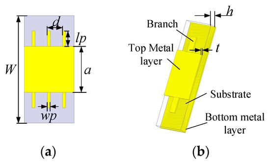
Figure 2.
Configurations of MC-TL. (a) Top view. (b) Three-dimensional structure of the unit cell.
The width and depth of the grooves are denoted as wp and lp, respectively. The period of the SSPPs element is represented by d, while the substrate thickness is indicated as h. Both the top and bottom metal layers have a thickness of t. In this paper, t = 0.018 mm. It should be noted that the impact of t on the electric field distribution is negligible. Research has demonstrated that periodic metallic grooves can sustain and propagate a surface plasmon mode in microwave frequencies when wp and lp are significantly smaller than the operational wavelength. The dispersion relationship of these SSPPs is documented in [24].
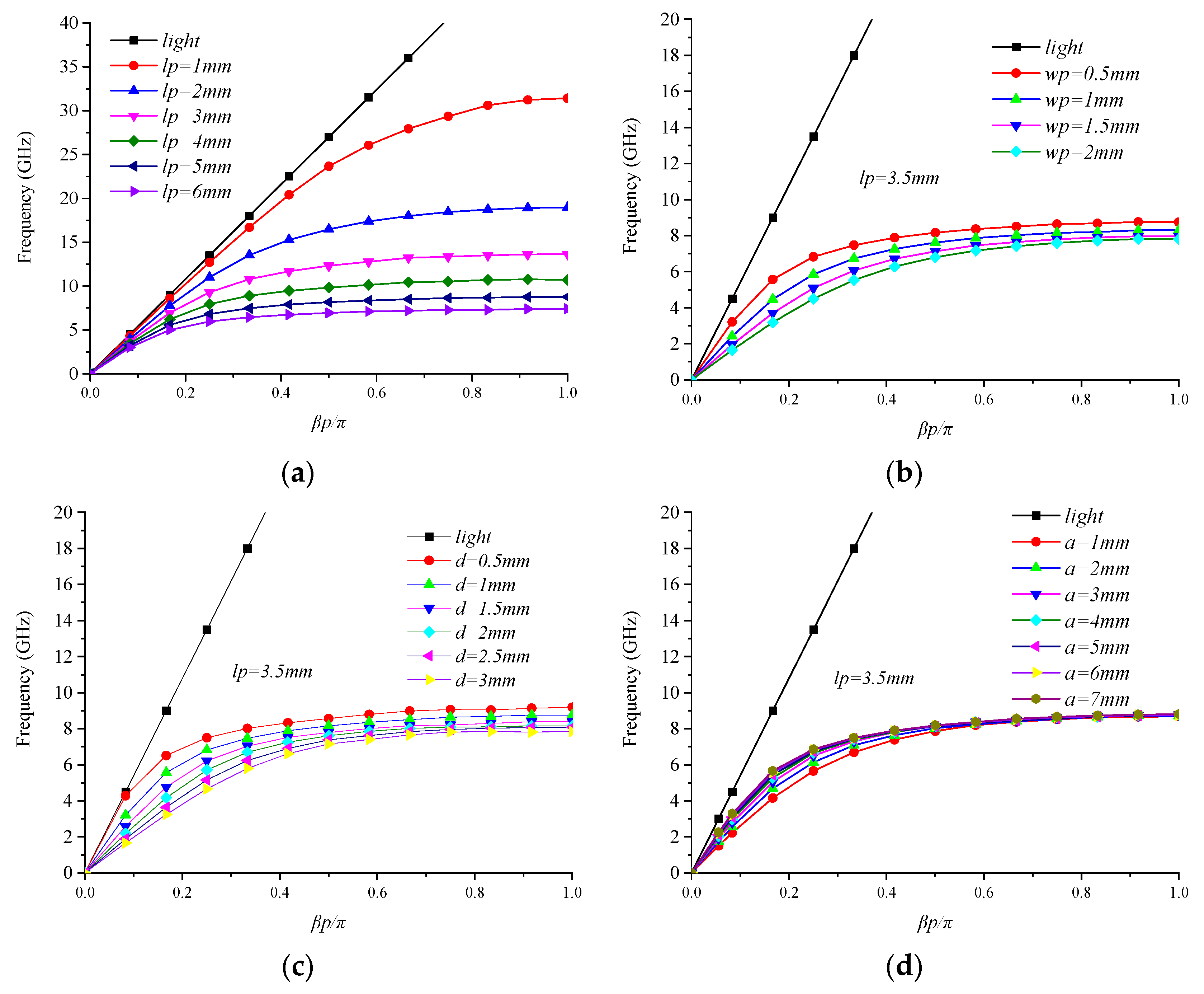
where β is the propagation constant of the SSPPs mode, and k0 = ω/c. The dispersion curve of this SSPP was also analyzed using Ansys HFSS, as shown in Figure 3. Figure 3a shows the dependence of dispersion relations for the fundamental SSPPs mode on an lp ranging from 1 to 6 mm while keeping a = 6 mm, wp = 0.4 mm, d = 1.6 mm, and h = 0.508 mm. h is the thickness of the dielectric substrate, which does not change The substrate is a Taconic RF-35 substrate. It can be observed that the curves exhibit decreased upper cutoff frequencies as the groove depth lp increases. As shown in Figure 3b,c, when a = 6 mm, lp = 3.5 mm, the wp and d will also affect the cutoff frequencies. The smaller the values of wp or d, the higher the cutoff frequency will be. The cutoff frequency is almost unaffected by a at a low-frequency passband, as shown in Figure 3d, where the rest of the other parameters are fixed at wp = 0.4 mm, d = 1.6 mm, and lp = 3.5 mm. Based on this phenomenon, we can combine SSPPs and a CSIW, and obtain the conclusion that the TE10 mode does not affect the surface plasmon mode.
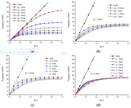
Figure 3.
Dispersion relations for the fundamental SSPP mode of the MC-TL. (a) With different lengths of groove lp. (b) With different widths of branch wp. (c) With different periods of branch d. (d) With different widths of CSIW a.
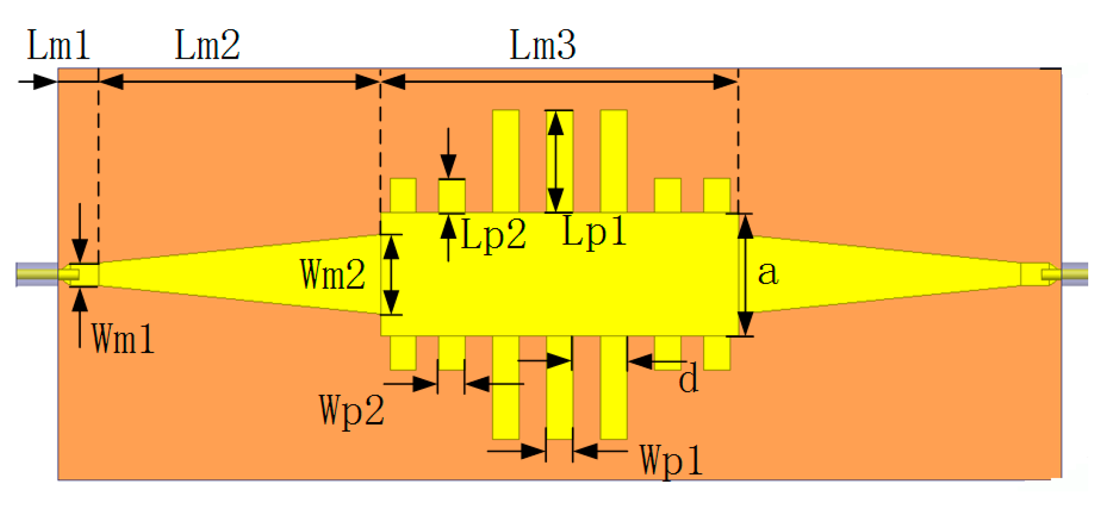
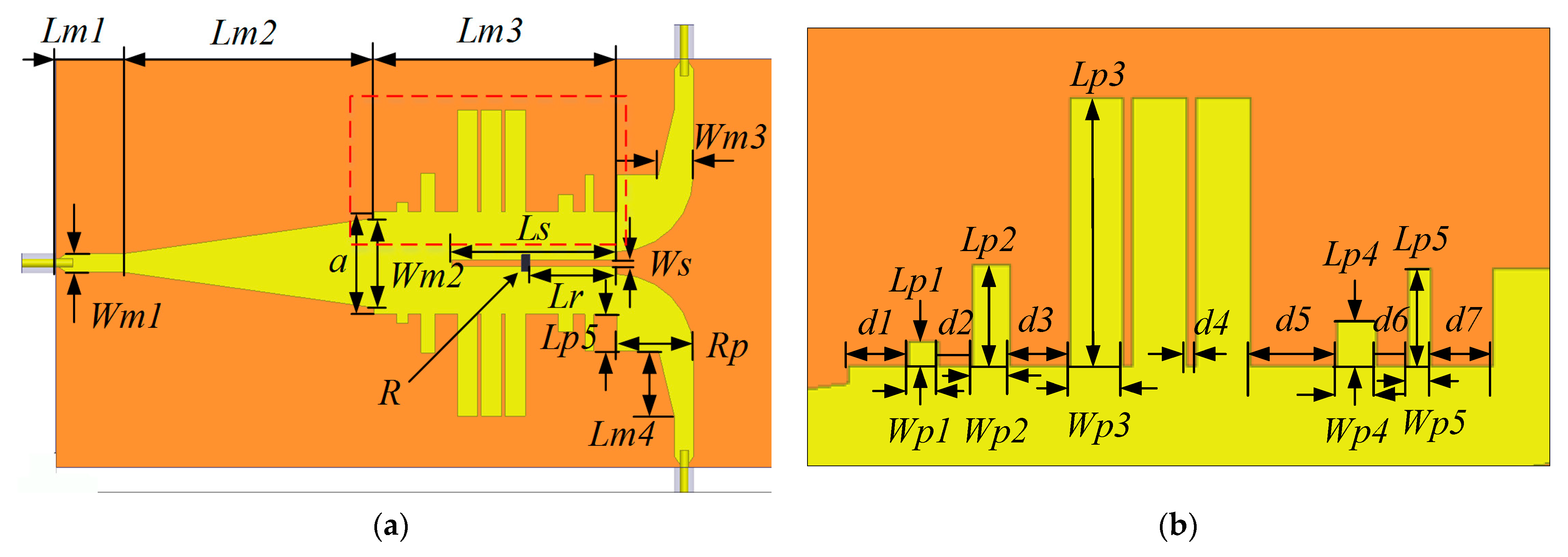
The dimensions of the substrate-integrated waveguide and the length of the quarter-wavelength open-circuit stub line were computed with respect to the high-frequency passband. Subsequently, the width and spacing of the open-circuit stub lines were established considering the characteristics of the spoof surface plasmon polaritons (SSPPs). Finally, in order to realize a composite mode transmission line composed of the volume elements of the SSPPs and CSIW excited simultaneously from the microstrip line ports, a microstrip line with step transitions of open-stub lines and tapering lines was investigated. The low-pass frequency was up to 5 GHz, as shown in Figure 3, and lp should be set first. When the length of lp is determined, the low-frequency passband of this structure is narrow, and with big discontinuity in the circuit. So, in the input direction, grooves are used in the form of steps to realize the impedance matching, as shown in Figure 4. As can be seen from the figure, the whole circuit has a symmetrical structure that adopts coaxial input; the length of the feed port is Lm1, and the width is Wm1. Then, the circuit is followed by the conical microstrip line for impedance matching. The length of the wide side of the microstrip line is Wm2 and its length is Lm2, and the lengths of the open-stub lines are Lp2 and Lp1 and their widths are Wp2 and Wp1, respectively. The distance between the open-stub lines is d.
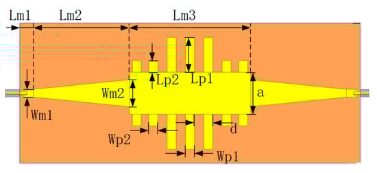
Figure 4.
Schematic of the configuration of the proposed MC-TL.
3. MC-TL Design
To achieve a suitable operating frequency for 5G communication, it is essential to create a dual-band transmission line (TL) system functioning within the ranges of 3 GHz to 5 GHz and 25 GHz to 30 GHz. Given that the surface plasmon polariton (SSPP) mode exhibits low-pass characteristics and the TE10 mode showcases high-pass traits, we devised SSPPs for operation between 3 GHz and 5 GHz and a CSIW for utilization at 25 GHz to 30 GHz.
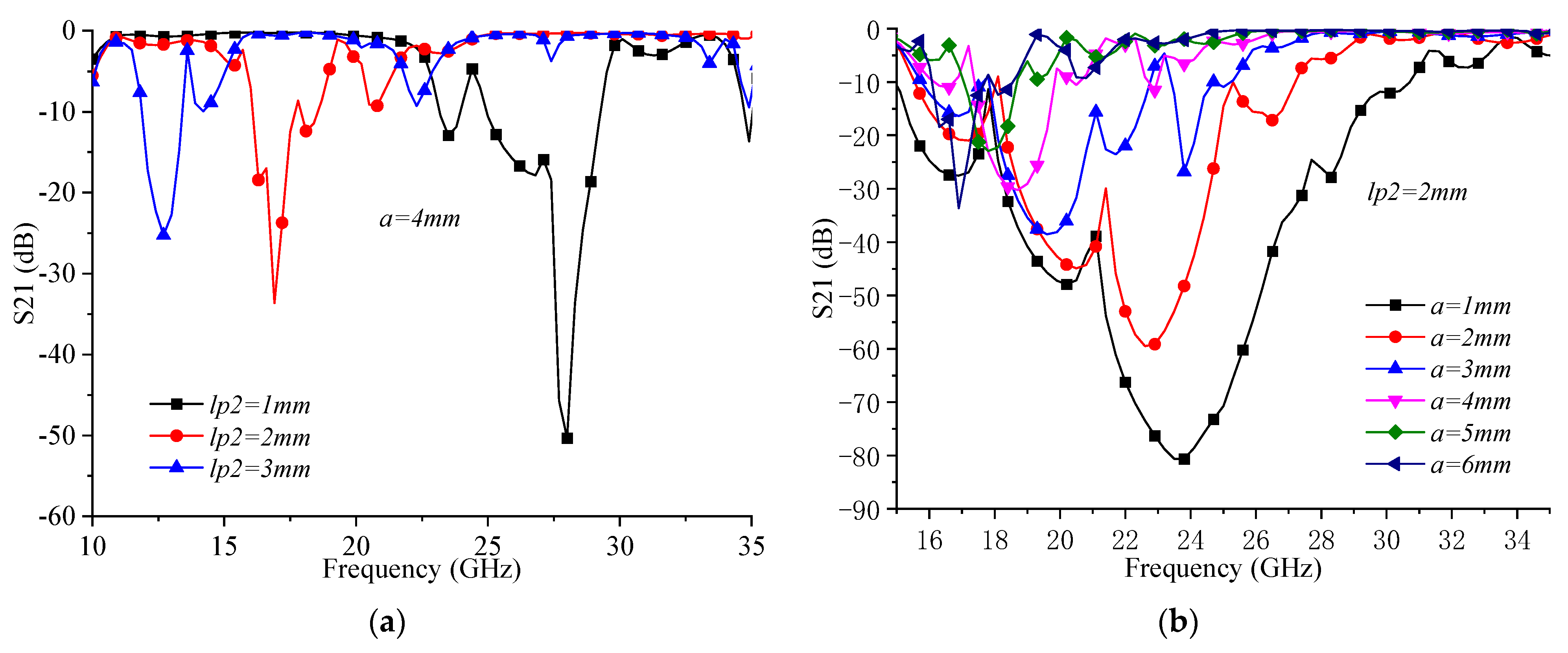
With the help of HFSS 2023 software, using the wave port to excite the MC-TL, as shown in Figure 1d, S21 can be obtained, as shown in Figure 5. It can be seen that the lower cutoff frequency of the filter is determined by lp2 and a at a high-frequency passband. While increasing the width of the CSIW a makes the lower cutoff frequency of the high-frequency passband shift to the left, as a decreases, the operating frequency will increase and a much larger frequency ratio will be obtained, such as how a SIW does.
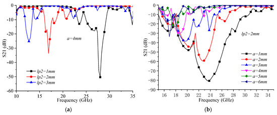
Figure 5.
Simulated transmission coefficients (S21) of the MC−TL in high-frequency passband: (a) with different lengths of lp2; (b) with different widths of the CSIW.
In this MC-TL structure, the low-frequency passband is determined by the length, width, and period of the grooves, as seen in Figure 3. Meanwhile, the high-frequency passband is determined by the width of the CSIW and the length of the first two grooves, as seen in Figure 5.
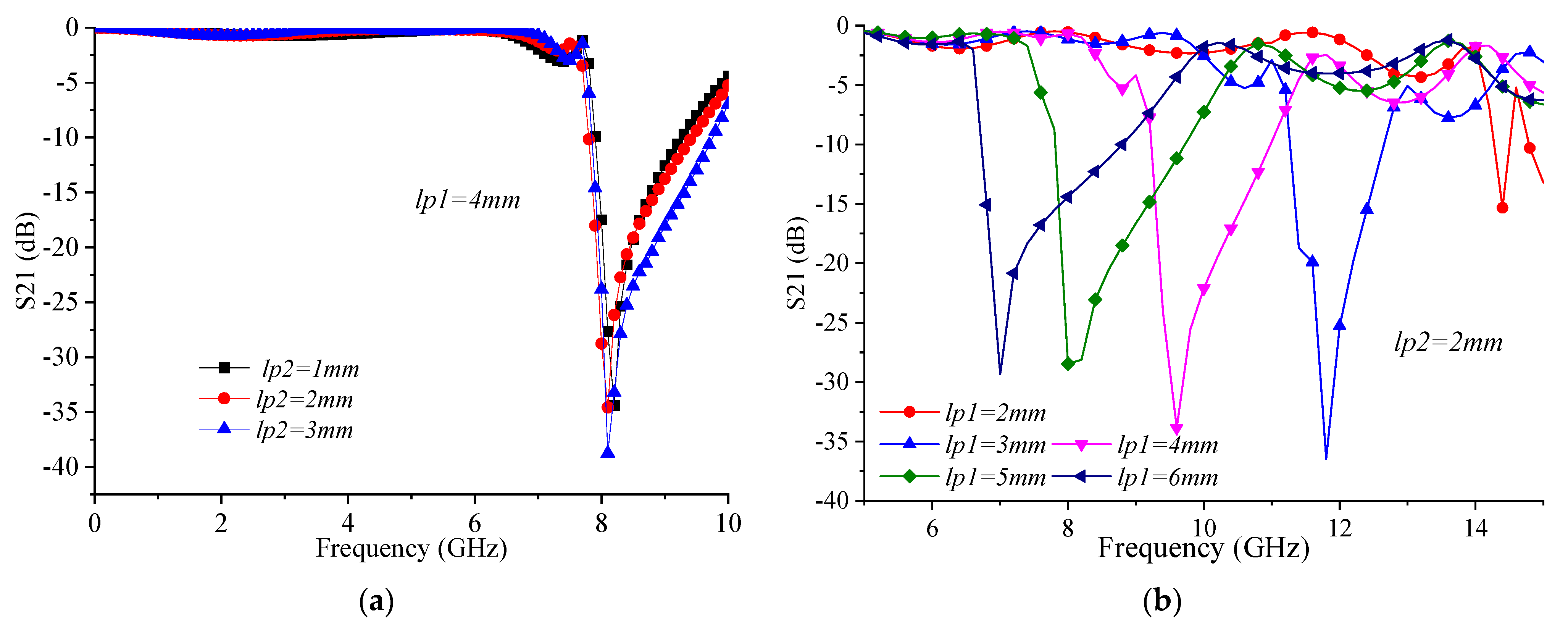
As shown in Figure 6a, in the low-frequency passband, lp2 can affect the insertion loss when lp1 = 4 mm; lp1 affects the cutoff frequency of the low-frequency passband when lp2 = 2 mm, as shown in Figure 6b.
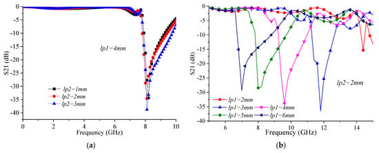
Figure 6.
Simulated transmission coefficients (S21) of the MC−TL with different lengths of lp1 and lp2: (a) low-frequency passband; (b) high-frequency passband.
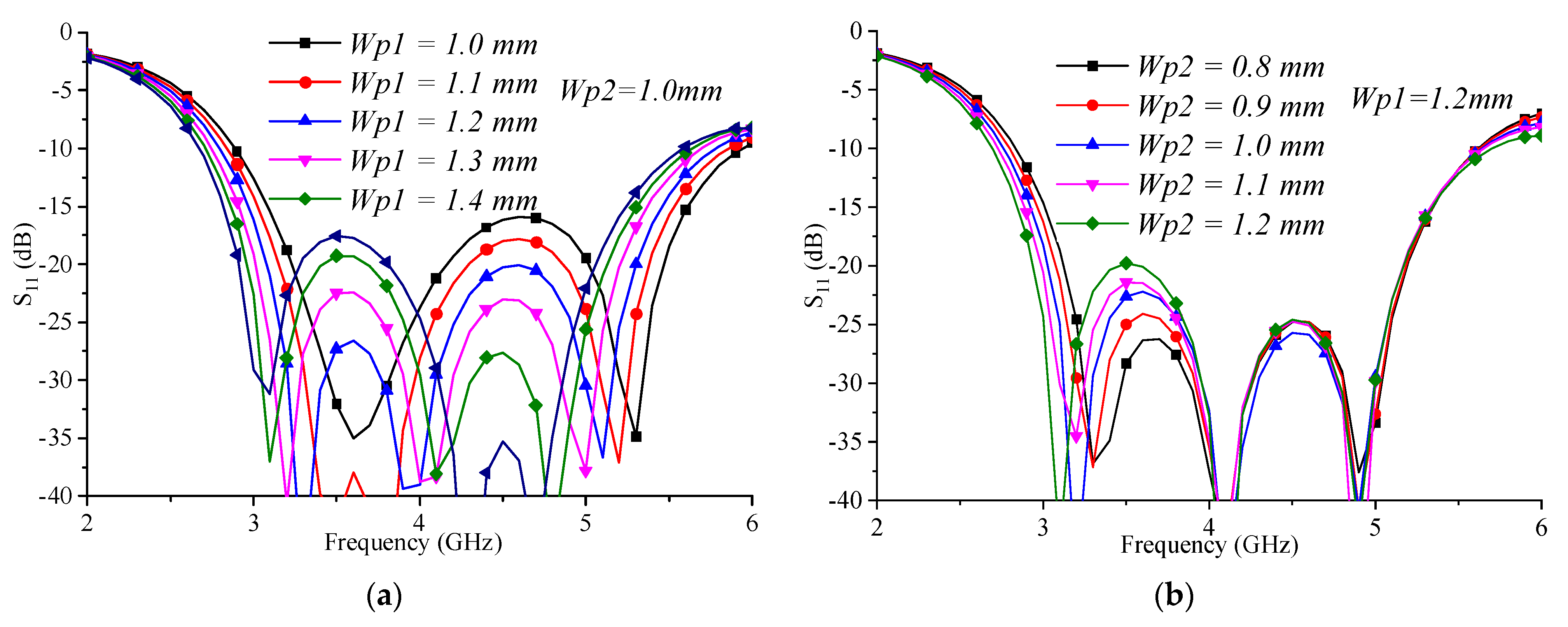
After the high-frequency passband and low-frequency passband are settled, Wp1, Wp2 can be used to adjust the return loss in the low-frequency passband, as shown in Figure 7. Wp1 affects the amplitude characteristics in the passband more when Wp2 = 1.0 mm, lp1 = 4 mm, and lp2 = 2 mm, while Wp2 affects only the first pole in the passband when Wp1 = 1.2 mm, lp1 = 4 mm, and lp2 = 2 mm. This shows that the unified grooves affect the low-frequency passband much more than the step part.

Figure 7.
Simulated return loss of the low-frequency passband of the MC−TL: (a) with different Wp1 values; (b) with different Wp2 values.
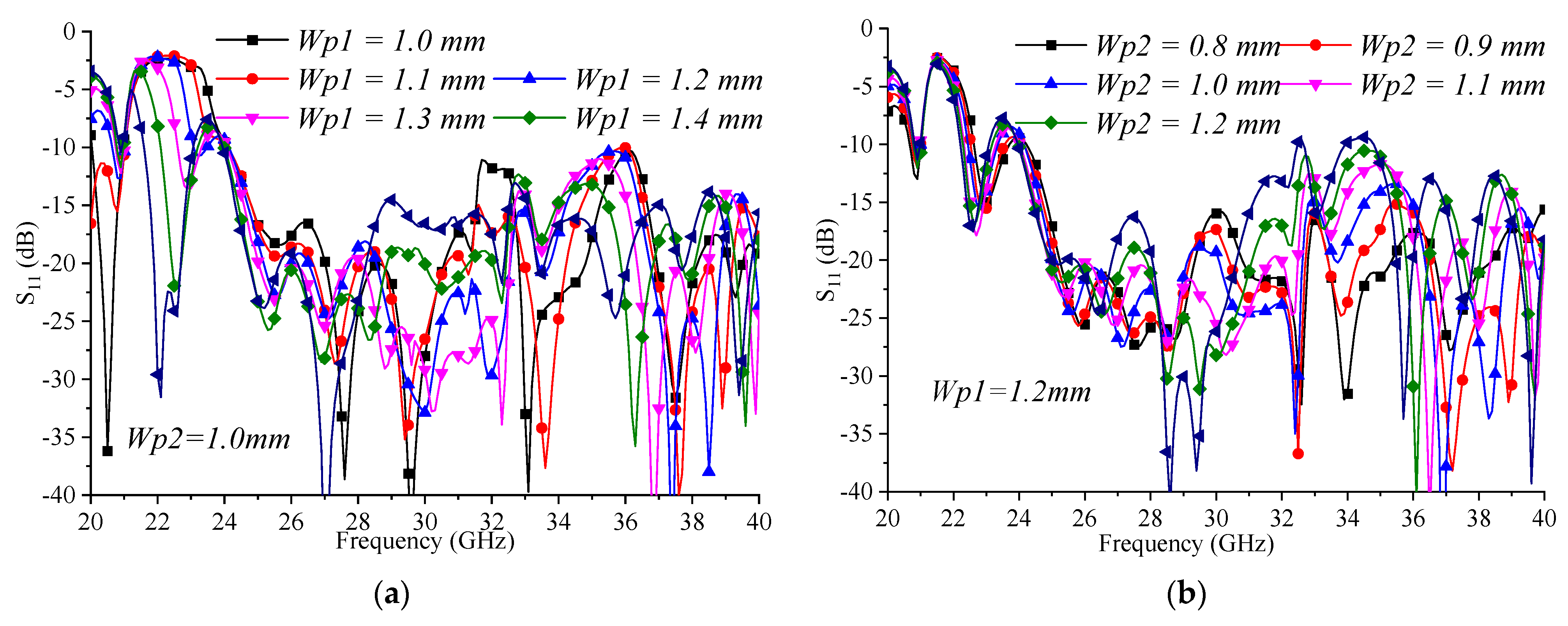
As depicted in Figure 8, the capacitive reactance equivalence of the transition structure within the open-stub line plays a significant role in determining the transmission poles of the high-frequency passband. Moreover, the impedance matching between the transition structure and the open-stub line is primarily influenced by the first-order characteristics of the open-stub line.
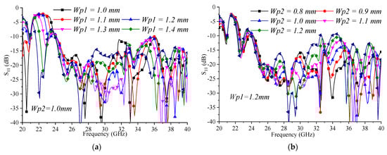
Figure 8.
Simulated return loss of the high-frequency passband of MC−TL (a) with different Wp1, (b) with different Wp2.
The transition from the microstrip to substrate-integrated waveguide (SIW) facilitates the seamless conversion of the quasi-TEM mode of the microstrip into the TE10 mode of the CSIW. In incorporating a graded length of grooves on either side of the CSIW transition, impedance matching is achieved to efficiently convert the quasi-TEM mode of the microstrip to the surface plasmon polariton (SSPP) mode. It is crucial that the length of the impedance matching section Lm2 corresponds to a quarter wavelength of the low-pass frequency to ensure optimal performance.
The width Wm2 at the joint between the microstrip line and the MC-TL is chosen so that the impedance between the two structures is matching. The traditional microstrip lines are used to connect the input–output 50 Ω microstrip lines as their broadband virtue, where Wm1 is set to meet the impedance of the microstrip line equal to 50 Ω. The 2.92 mm coaxial connector, which is also 50 Ω, is also considered in the design.
In order to improve the impedance matching and TL performance, we carried out parameter optimization and set the optimized geometric parameters as listed in Table 1. All optimization parameter values were obtained by first setting reasonable initial values on the basis of formulas, and then by setting the value range of parameter values conducive to the target optimization function of electromagnetic simulation software HFSS.

Table 1.
Dimensions of the proposed structure (UNIT: millimeter).
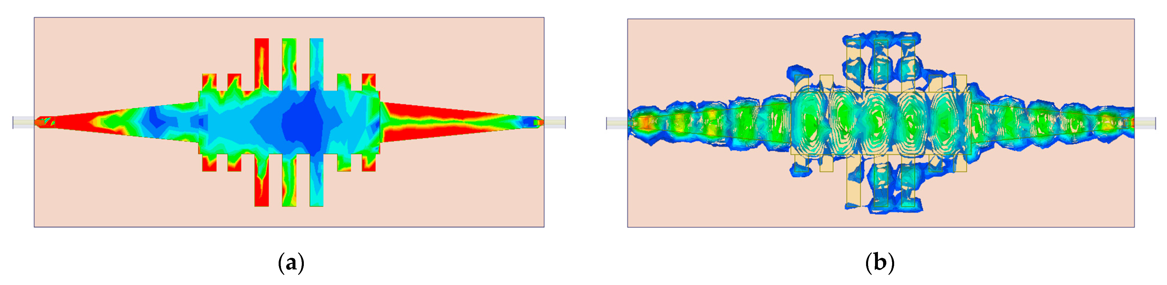
The electric field distribution of the MC-TL is also illustrated in Figure 9 for comparison purposes. As depicted in Figure 9a, it becomes evident that within the low-frequency passband, the microwave signal solely propagates through the SSPP structure. The energy is highly localized and primarily travels along the interface between air and metal, resembling natural surface plasmon materials. As shown in Figure 9b, within the high-frequency passband, the microwave signal propagates through the substrate connecting both top and bottom metal layers, functioning similarly to a CSIW [22].
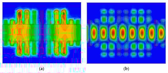
Figure 9.
Open-stub substrate-integrated waveguide large-frequency ratio composite mode transmission line field diagrams: (a) low-frequency passband; (b) high-frequency passband.
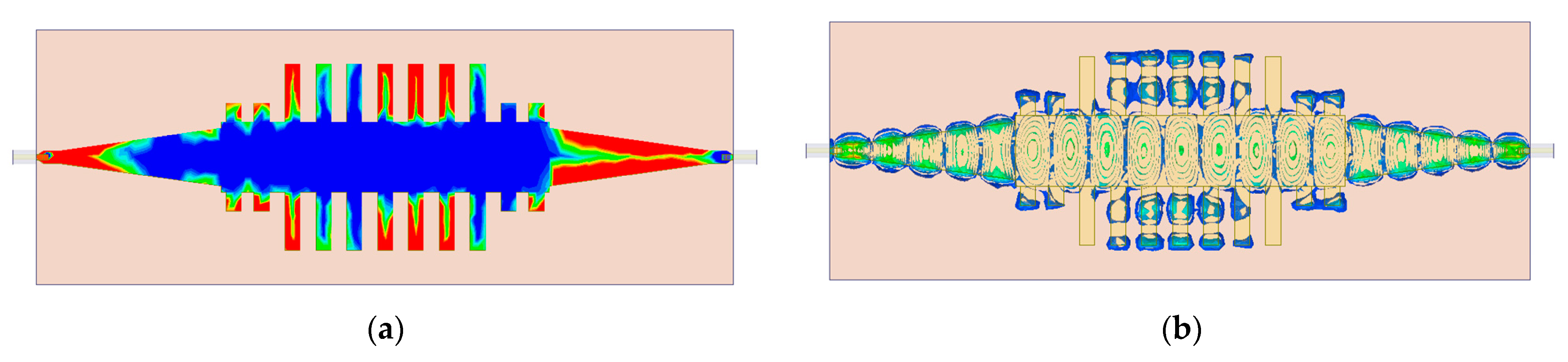
As shown in Figure 10 and Figure 11, the characteristic of the proposed MC-TL structure with seven grooves remains basically the same as the structure with three grooves. Of course, with more grooves, it is clear that the waves are better settled. In increasing the length of the MC-TL, that is, in increasing its transmission phase, its working characteristics are kept unchanged.
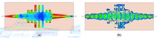
Figure 10.
Simulated E-field distribution with three grooves: (a) at 4 GHz; (b) at 27 GHz.
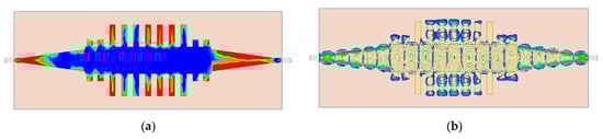
Figure 11.
Simulated E-field distribution with seven grooves: (a) at 4 GHz; (b) at 27 GHz.
4. Simulation and Measurement of MC-TL
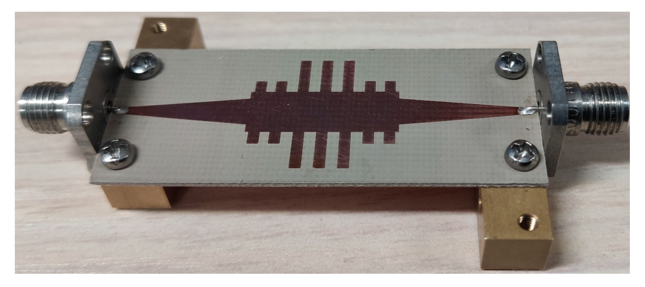
The proposed MC-TL was fabricated using a Taconic RF-35 substrate with a relative permittivity of εr = 2.2 and a thickness of h = 0.508 mm, and a loss tangent tanδ = 0.0018. The properties of the proposed TLs were verified through an experimental measurement using a vector network analyzer N5244A.
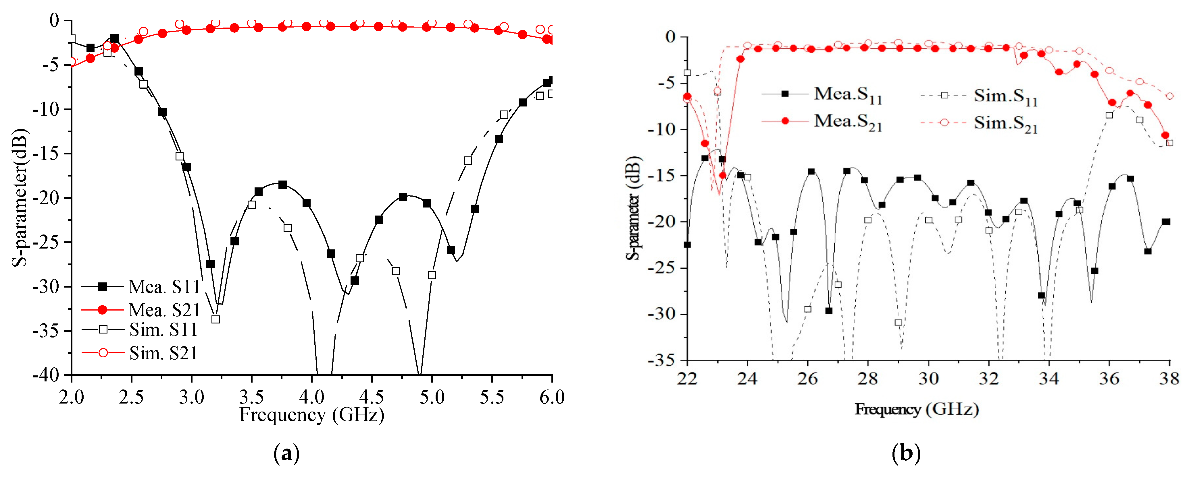
The fabricated MC-TL is depicted in Figure 12, while the simulated and measured frequency response of the MC-TL can be observed in Figure 13. The operational bandwidth of the MC-TL spans from 3.0 to 5.2 GHz, exhibiting a return loss below −18 dB and an insertion loss under 0.3 dB, as illustrated in Figure 13a. Remarkably, the measured results align closely with the simulated outcomes. In Figure 13b, both the measured and simulated performances of the MC-TL within its high-frequency passband are presented. Within this range, namely from 23 to 40 GHz (the maximum measuring range of our instrument), a return loss below −15 dB can be achieved. However, it should be noted that above this frequency threshold, specifically beyond approximately 33 GHz, resonance occurs due to the periodicity of the microwave circuitry known as the SSPP structure, which also leads to slight radiation and consequently worsens the insertion loss.
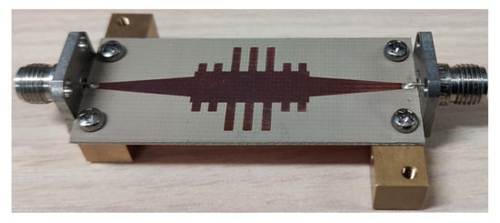
Figure 12.
Photograph of the fabricated MC-TL.
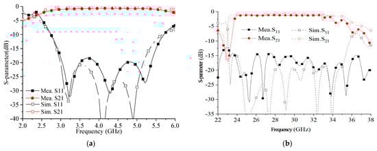
Figure 13.
Simulated and measured S-parameters of MC-TL: (a) low-frequency passband; (b) high-frequency passband.
As per the aforementioned report, the bandwidth of the MC−TL spans across both existing mobile communication systems and a future 5G mobile communication system within its lower and higher frequency passbands.
With this configuration, the MC−TL was energized and concluded to use the microstrip line. Consequently, it can be readily incorporated with other planar microwave circuits owing to the adaptable nature of the microstrip line.
Table 2 outlines a contrast between various types of mode composite transmission line transition structures to showcase the MC-TL’s superiority.
Table 2.
Comparison of different mode composite transmission line transition structure.
5. Dual-Band Power Divider Based on MC-TL
The geometry of the proposed MC-TL power divider is shown in Figure 14. The power divider based on the MC-TL can work in both low-frequency passbands and high-frequency passbands, and is hence called a dual-band power divider. The size of it is 22.34 mm × 45.18 mm.
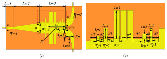
Figure 14.
Schematic of (a) the proposed dual-band power divider and (b) the SSPP part.
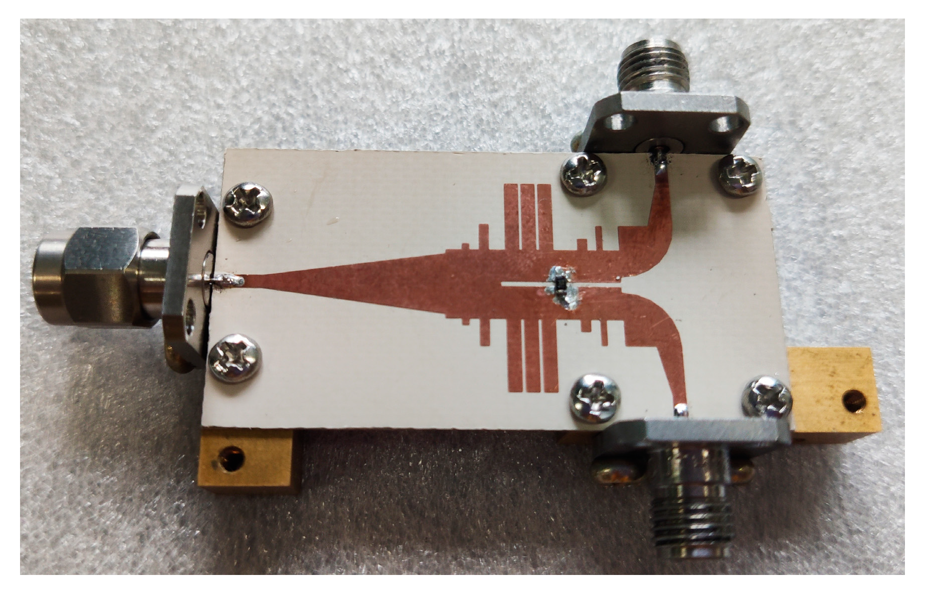
Based on the Wilkinson power divider [25], a single resistor was utilized to achieve isolation between the two output ports. The distance from the resistance to the bifurcation corresponds to one-quarter of both the surface plasmon mode and TE10 mode wavelengths. After optimization using Ansys HFSS, the power divider’s geometry parameters were obtained; these are presented in Table 3, encompassing a total of 29 optimized parameter values. Figure 15 displays a photograph of the prototype. Subsequently, with an installed resistor value of 28 Ω, the power divider underwent testing using the vector network analyzer N5244A. Figure 16 illustrates simulated and measured reflection coefficients, transmission coefficients, and the isolation between each output port.
Table 3.
Dimensions of the dual-band power divider (Unit: millimeter).

Figure 15.
Photograph of the fabricated dual-band power divider.
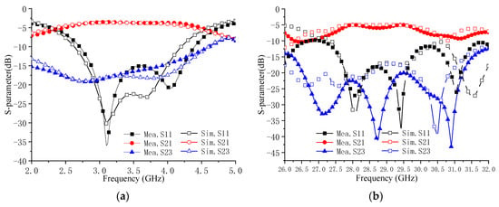
Figure 16.
Simulated and measured S-parameters of dual-band power divider: (a) low-frequency passband; (b) high-frequency passband.
From Figure 16a, it is evident that S11 remained below −15 dB within the frequency range of 2.8 GHz to 4.2 GHz, while S21 measured at −3.7 dB and S23 stayed below −15 dB across this same frequency range. As shown in Figure 16b, S11 maintained levels below −15 dB from 27.6 GHz to 29.7 GHz; meanwhile, S21 recorded −5.97 dB, and S23 remained below −17 dB throughout all operating frequencies.
The variation in the isolation performance stems from discrepancies between the resistance location during manual welding and its simulated position. On the other hand, the insertion loss is primarily a result of the microstrip line utilized as a transition line from the coaxial line to the multilayered composite transmission line (MC-TL). At a high frequency, the insertion loss caused by the microstrip line will be more and more obvious. When a discontinuous structure such as a corner is realized by the microstrip line, the radiation of the quasi-TEM in the air will increase again, which will increase the insertion loss of the circuit. This is why MC-TLs are demanded, to replace microstrip lines and realize miniaturization in high frequency ratios.
In Table 4, the proposed dual-band power divider is compared with previously reported dual-band power dividers. It can be seen that the composite mode transmission line dual-passband power divider proposed in this paper adopts fundamental mode transmission on two different transmission lines and uses a unified port for excitation, with a larger frequency ratio, and has better application prospects.
Table 4.
Comparison with previous dual-band power dividers.
6. Conclusions
This study introduced a new MC-TL designed for 5G communication systems, merging SSPP and CSIW methodologies in an exceptionally compact single-layer structure. Additionally, a dual-band power divider utilizing the MC-TL was developed as a specific application, allowing independent operation within distinct frequency bands. The SSPP part supports the surface plasmon mode as its fundamental mode, while a TE10 mode signal is transmitted in the CSIW part. The single-layer composite structure and mode-separation characteristics of the MC-TL make it a possible application for multifunction and multi-band microsystems. The characteristics were analyzed for the MC-TL, and the dual-band power divider was fabricated based on a possible application of the MC-TL, which demonstrates the feasibility and practicality of the proposed MC-TL. Meanwhile, the top conductor of the structure was isolated from the ground at the DC permitting integration of active devices at the open edge. The prospective usage of the MC-TL appears bright, given its ability to amalgamate the characteristics of SSPPs and a CSIW for the creation of compact, versatile microwave circuits in multi-band microwave and millimeter-wave systems.
By incorporating a spoof surface plasmon (SSPP) mode structure onto a conventional substrate-integrated waveguide (SIW) power divider, a unique configuration was established, enabling the power divider to operate simultaneously at both 3 GHz and 28 GHz. This innovative design functions in surface plasmon (SP) mode at 3 GHz and in TE10 mode at 28 GHz. Notably, the frequencies of both the upper and lower bands are individually adjustable, allowing for an expanded frequency ratio range between the bands. To validate this concept, a prototype power divider was fabricated, capable of accommodating the frequency requirements of fifth-generation communication systems. Through extensive simulation and experimental testing, the implemented design successfully delivered the anticipated outcomes. It must be noted that in the actual device, how the different bands are coupled/separated from the proposed structure is still a challenging problem to solve.
Author Contributions
Methodology, K.S.; Validation, Y.Z.; Writing—original draft, L.F. All authors have read and agreed to the published version of the manuscript.
Funding
This research was funded by the National Natural Science Foundation of China, grant number 62171097.
Data Availability Statement
All the materials used in the study are mentioned within the article.
Conflicts of Interest
The authors declare no conflicts of interest.
References
- Halak, B.; El-Hajjar, M.; Toma, O.H.; Cheng, Z. Energy-Efficient Hardware Implementation of an LR-Aided K-Best MIMO Decoder for 5G Networks. J. Low Power Electron. Appl. 2016, 6, 12. [Google Scholar] [CrossRef]
- Pi, Z.; Khan, F. An introduction to millimeter-wave mobile broad-band systems. IEEE Commun. Mag. 2011, 49, 101–107. [Google Scholar] [CrossRef]
- Siddiqui, M.F.; Maheshwari, M.K.; Raza, M.; Masud, A.R. Design and Optimization of an Ultra-Low-Power Cross-Coupled LC VCO with a DFF Frequency Divider for 2.4 GHz RF Receivers Using 65 nm CMOS Technology. J. Low Power Electron. Appl. 2023, 13, 54. [Google Scholar] [CrossRef]
- Nguyen, X.V.L.; Gerges, T.; Bevilacqua, P.; Duchamp, J.-M.; Benech, P.; Verdier, J.; Lombard, P.; Linge, P.U.; Mieyeville, F.; Cabrera, M.; et al. Radio-Frequency Energy Harvesting Using Rapid 3D Plastronics Protoyping Approach: A Case Study. J. Low Power Electron. Appl. 2023, 13, 19. [Google Scholar] [CrossRef]
- Guo, J.; Djerafi, T.; Wu, K. Mode composite waveguide. IEEE Trans. Microw. Theory Tech. 2016, 64, 3187–3197. [Google Scholar] [CrossRef]
- Li, Y.; Wang, J. Dual-band leaky-wave antenna based on dual-mode composite microstrip line for microwave and millimeter-wave applications. IEEE Trans. Antennas Propag. 2018, 66, 1660–1667. [Google Scholar] [CrossRef]
- Xiang, B.J.; Zheng, S.Y.; Wong, H.; Pan, Y.M.; Wang, K.X.; Xia, M.H. A Flexible Dual-Band Antenna with Large Frequency Ratio and Different Radiation Properties over the Two Bands. IEEE Trans. Antennas Propag. 2018, 66, 657–667. [Google Scholar] [CrossRef]
- Su, Y.; Lin, X.Q.; Yu, J.W.; Fan, Y. Mode composite coplanar waveguide. IEEE Access 2019, 7, 109278–109288. [Google Scholar] [CrossRef]
- Wu, K.; Deslandes, D.; Cassivi, Y. The substrate integrated circuits—A new concept for high-frequency electronics and optoelectronics. In Proceedings of the 6th International Conference on Telecommunications in Modern Satellite, Cable and Broadcasting Service (TELSIKS), Nis, Yugoslavia, 1–4 October 2003; Volume 1, pp. P-III–P-X. [Google Scholar]
- Heidari, H.R.; Rezaei, P.; Kiani, S.; Taherinezhad, M. A monopulse array antenna based on SIW with circular polarization for using in tracking systems. AEU-Int. J. Electron. Commun. 2023, 162, 154563. [Google Scholar] [CrossRef]
- Kumar, L.; Nath, V.; Reddy, B.V.R. A wideband substrate integrated waveguide (SIW) antenna using shorted vias for 5G communications. AEU-Int. J. Electron. Commun. 2023, 171, 154879. [Google Scholar] [CrossRef]
- Abdolhamidi, M.; Shahabadi, M. X-band substrate integrated waveguide amplifier. IEEE Microw. Wirel. Compon. Lett. 2008, 18, 815–817. [Google Scholar] [CrossRef]
- Anand, S.; Theetharappan, R. Metamaterial and SIW inspired isolating fences for lateral de-coupling in MIMO antenna. AEU-Int. J. Electron. Commun. 2023, 166, 154667. [Google Scholar] [CrossRef]
- Pendry, J.B.; Martín-Moreno, L.; Garcia-Vidal, F.J. Mimicking surface plasmons with structured surfaces. Science 2004, 305, 847–848. [Google Scholar] [CrossRef] [PubMed]
- Shen, X.; Cui, T.J.; Martin-Cano, D.F.; Garcia-Vidal, J. Conformal surface plasmons propagating on ultrathin and flexible films. Proc. Nat. Acad. Sci. USA 2013, 110, 40–45. [Google Scholar] [CrossRef] [PubMed]
- Ge, S.; Zhang, Q.; Chiu, C.-Y.; Chen, Y.; Murch, R.D. Single-side-scanning surface waveguide leaky-wave antenna using spoof surface plasmon excitation. IEEE Access 2018, 6, 66020–66029. [Google Scholar] [CrossRef]
- Kianinejad, A.; Chen, Z.N.; Qiu, C.-W. Design and modeling of spoof surface plasmon modes-based microwave slow-wave transmission line. IEEE Trans. Microw. Theory Tech. 2015, 63, 1817–1825. [Google Scholar] [CrossRef]
- Pan, B.C.; Cui, T.J. Broadband decoupling Network for Dual-Band Microstrip Patch Antennas. IEEE Trans. Antennas Propag. 2017, 65, 5595–5598. [Google Scholar] [CrossRef]
- Guan, D.-F.; You, P.; Zhang, Q.; Xiao, K.; Yong, S.-W. Hybrid Spoof Surface Plasmon Polariton and Substrate Integrated Waveguide Transmission Line and Its Application in Filter. IEEE Trans. Microw. Theory Tech. 2017, 65, 4925–4932. [Google Scholar] [CrossRef]
- Shen, S.; Xue, B.; Yu, M.; Xu, J. Integrated Mode Composite Transmission Line. IEEE Access 2019, 7, 41479–41491. [Google Scholar] [CrossRef]
- Ye, L.; Chen, Y.; Da Xu, K.; Li, W.; Liu, Q.H.; Zhang, Y. Substrate Integrated Plasmonic Waveguide for Microwave Bandpass Filter Applications. IEEE Access 2019, 7, 75957–75964. [Google Scholar] [CrossRef]
- Chen, D.G.; Eccleston, K.W. Substrate integrated waveguide with corrugated wall. In Proceedings of the 2008 Asia-Pacific Microwave Conference, Macau, China, 16–20 December 2008; pp. 1–4. [Google Scholar] [CrossRef]
- Salehi, M.; Mehrshahi, E. A closed-form formula for dispersion characteristics of fundamental SIW mode. IEEE Microw. Wirel. Compon. Lett. 2011, 22, 4–6. [Google Scholar] [CrossRef]
- Talebi, N.; Shahabadi, M. Spoof surface plasmons propagating alonga periodically corrugated coaxial waveguide. J. Phys. D Appl. Phys. 2010, 43, 35302. [Google Scholar] [CrossRef]
- Wilkinson, E. An N-way hybrid power divider. IRE Trans. Microw. Theory Tech. 1960, MTT-8, 116–11118. [Google Scholar]
- Nguyen, M.G.; Nguyen, C.T.N.; Nguyen, T.H.; Morishita, H. Design of a Dual-Band Three-Way Power Divider with Unequally High Power Split Ratio. Radioengineering 2023, 32, 339. [Google Scholar] [CrossRef]
- Zhao, X.B.; Wei, F.; Zhang, P.F.; Shi, X.W. Mixed-Mode Magic-Ts and Their Applications on the Designs of Dual-Band Balanced Out-of-Phase Filtering Power Dividers. IEEE Trans. Microw. Theory Tech. 2023, 71, 3896–3905. [Google Scholar] [CrossRef]
- Salimi, P.; Jahromi, M.K.; Hossein, A.K.A. A Novel Design Method for Unequal Coupled Line Dual-Band Wilkinson Power Divider. Prog. Electromagn. Res. C 2023, 138, 175–189. [Google Scholar] [CrossRef]
- Danaeian, M. Novel single-layer dual-band half-mode substrate integrated waveguide filter and filtering power dividers with very compact sizes. Int. J. RF Microw. Comput.-Aided Eng. 2022, 32, e22951. [Google Scholar] [CrossRef]
- Mohra, A.S.S. Compact dual band Wilkinson power divider. Microw. Opt. Technol. Lett. 2008, 50, 1678–1682. [Google Scholar] [CrossRef]
- Liao, M.; Wu, Y.; Liu, Y.; Gao, J. Impedance-transforming dual-band out-of-phase power divider. IEEE Microw. Wirel. Compon. Lett. 2014, 24, 524–526. [Google Scholar] [CrossRef]


Disclaimer/Publisher’s Note: The statements, opinions and data contained in all publications are solely those of the individual author(s) and contributor(s) and not of MDPI and/or the editor(s). MDPI and/or the editor(s) disclaim responsibility for any injury to people or property resulting from any ideas, methods, instructions or products referred to in the content. |
© 2024 by the authors. Licensee MDPI, Basel, Switzerland. This article is an open access article distributed under the terms and conditions of the Creative Commons Attribution (CC BY) license (https://creativecommons.org/licenses/by/4.0/).