Abstract
In this paper, we present a 0.3 V body-driven operational transconductance amplifier (OTA) that exploits a biasing approach based on the use of a replica loop with gain. An auxiliary amplifier is exploited both in the current mirror load of the first stage of the OTA and in the replica loop in order to achieve super-diode behavior, resulting in low mirror gain error, which enhances CMRR, and robust biasing. Common-mode feedforward, provided by the replica loop, further enhances CMRR. Simulations in a 180 nm CMOS technology show 65 dB gain with 2 kHz unity-gain frequency on a 200 pF load when consuming 9 nW. Very high linearity with a 0.24% THD at 90% full-scale and robustness to PVT variations are also achieved.
1. Introduction
The evolution of technology leads to increasingly pervasive electronics, not only in the computing and communication fields, but also in biomedical applications [1,2,3] and in all aspects of daily life. In particular, the Internet of Things (IoT) [4], making objects ‘smart’ and able to intercommunicate, represents a milestone from the point of view of the pervasiveness of electronics. IoT nodes include sensor capabilities, computing, and wireless communications, thus presenting potential applications in a very broad range of fields such as healthcare, agriculture, automotive, and industrial manufacturing [5,6,7,8,9,10].
IoT nodes are mixed-signal systems that include analog signal conditioning, digital processing, and wireless communication, and are often energy-autonomous. They therefore require a drastic reduction of power consumption, since they take their energy from batteries that are required to be small [11] or directly from the environment, exploiting energy harvesting techniques [12,13,14]. Things are similar in the case of biomedical devices, particularly implantable ones [15,16,17], for which substitution of the battery is not a viable solution or at least requires a surgical operation.
Reduction of the supply voltage is one of the available options to reduce power dissipation; moreover, in the case of energy-harvesting systems, which typically provide voltages in range of hundreds of mV [13], reduction of supply voltage would reduce the need for step-up converters and simplify power management. In CMOS technology, reduction of the supply voltage to 0.3–0.5 V leads the devices to operate in moderate or weak inversion. This results in a drastic drop in power consumption and transistor speed that is still compatible with applications utilizing signals with bandwidth up to hundreds of kHz and however no more than some MHz. This context has led to a boost of research interest in the field of ultra-low voltage (ULV) and ultra-low power (ULP) electronics [18,19].
Analog interfaces are a critical function in IoT nodes and biomedical circuits, and the unbuffered operational amplifier (UOPA), also often denoted as the “operational transconductance amplifier” (OTA) in the literature, is a fundamental building block in such applications. The UOPA is also one of the most challenging blocks to design in ULV/ULP applications due to the competitive requirements for gain, bandwidth, efficiency and robustness under process, supply voltage, and temperature (PVT) variations [20,21]. UOPAs and proper OTAs have widespread applications in biomedical and IoT systems, including in the analog input interface, in the design of amplifiers and filters, in drive actuators, as buffer references for the analog-to-digital converter (ADC), and in the design of low-dropout regulators (LDOs). Limited bandwidths are often needed, but some of these applications require the driving of large capacitive loads. The extremely low supply voltage does not allow for the exploitation of traditional design approaches such as tailed differential pairs and cascoding, and several design techniques have been studied for the design of efficient ULV OTAs. Solution based on a fully-digital approach (DIGOTA) [22,23,24] or operating in the time domain [25,26] have been proposed, but most of these techniques exploit analog approaches such as body-driving [27,28,29,30,31,32,33,34,35,36,37,38,39,40,41,42,43,44,45], floating-gate [46] and floating-body [47] devices, and inverter-based architectures [48,49,50,51]. The latter are often suitable for implementation using digital standard-cell libraries [52,53,54,55], thus simplifying the layout through the use of automatic place-and-route CAD tools and easing design portability among different technologies.
The lack of a tail current source makes biasing more sensitive to PVT variations and results in a drastic worsening of the common-mode rejection ratio (CMRR). Body biasing [21] has been proposed in the literature as a substitute for the tail generator, but the reduced supply voltage and the low body transconductance gain limit its performance in coping with PVT variation. In the case of body-driven OTAs, the gate terminals are available for biasing, and this places the bias current within the limit of the precision of the resulting current mirror. This is affected not only by device mismatches but also by different drain-source voltages, resulting in the dispersion of performance under PVT variations.
In the case of fully differential stages, CMRR is determined by the common-mode feedback (CMFB) loop gain. Differential-to-single-ended (D2S) stages are typically designed with a (pseudo)-differential pair loaded by a current mirror; without the tail current generator, CMRR entirely relies on the precision of the current mirror load. Even in the ideal case of perfectly matched devices, the output resistance of the transistors results in a gain error and hence limits CMRR. Using a fully differential input stage with common-mode feedback [40,44] improves CMRR in the nominal case but results in larger variations under mismatches due to common-mode to differential-mode conversion. A common-mode feedforward (CMFF) approach [29,38,56,57,58] can be used to improve CMRR in typical conditions, also reducing variability under PVT. In [43], an improved body-driven current mirror was proposed and applied to a ULV differential-to-single-ended (D2S) converter stage to improve its CMRR; a similar idea was applied in [53] to achieve high CMRR in a standard-cell-based OTA. The idea was to exploit an auxiliary amplifier to attenuate the gain error of the current mirror.
In this paper, we develop on this approach, and propose a two-stage body-driven ULV OTA with high CMRR and robust bias. The improvement of the auxiliary amplifier is exploited by the gate-driven current mirror of the input D2S stage to improve its CMRR; moreover, the same technique, together with a CMFF approach, is used in the biasing branch that generates the gate voltage for the gate biasing of the input stage. This not only allows for improvement of the CMRR, but also for the achievement of a bias point that is robust under PVT variations, thanks to the reference voltage exploited by the auxiliary amplifiers. The proposed solution entails utilizing an enhanced gate-driven current mirror (previously published in a body-driven configuration [43]) alongside a biasing approach that accurately fixes current and voltage.
2. Proposed Amplifier
This section introduces the proposed topology and presents a detailed analysis of its performance. Key features of the topology are the use of an enhanced current mirror, which helps with improving the common-mode rejection ratio (CMRR), and a replica bias loop that exploits auxiliary amplifiers to set bias current and node voltage with great robustness against variations. The bias approach is described in Section 2.2 to highlight its advantages in terms of robustness. The circuit is then analyzed considering its small-signal performance from the point of view of noise and differential-mode and common-mode behavior. This analysis shows how the proposed approach improves the CMRR of the proposed OTA, thanks to both the enhanced current mirror and the common-mode feedforward approach achieved through the replica bias. This approach also helps with reducing distortions, as shown in Section 2.6.
2.1. Topology Description
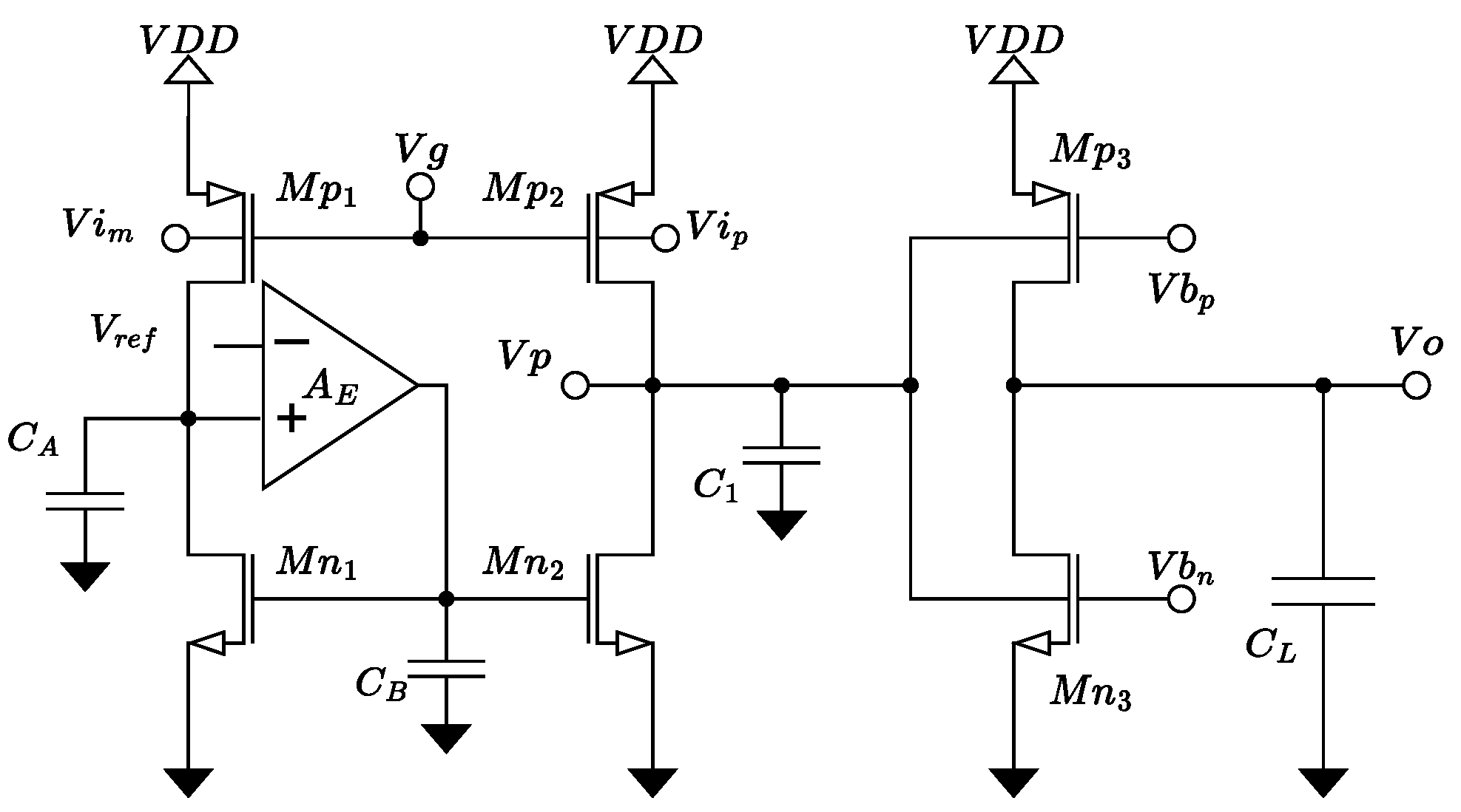
The proposed amplifier features a standard two-stage architecture, as shown in Figure 1; body-driving is exploited in both stages to allow for a rail-to-rail input common-mode range (ICMR) and keep gate terminals available for robust biasing. Both NMOS and PMOS body terminals are exploited as inputs of the second stage to enhance gain.
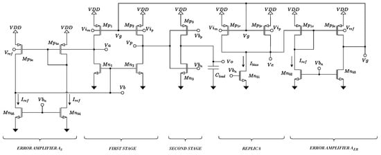
Figure 1.
Proposed two-stage OTA architecture with enhanced current mirror and replica bias.
With reference to Figure 1, the input stage is composed of transistors and . The input is applied to the body terminals of the PMOS devices, whose gate terminal is exploited to set the bias point. NMOS devices are used to form a current mirror load. To improve CMRR, the NMOS current mirror is enhanced through the use of an auxiliary amplifier that helps with reducing gain error. A simple single-stage body-driven auxiliary amplifier is used; it exploits a reference voltage that helps with achieving a robust bias point.
The first stage of the OTA is critical in achieving robust bias and high CMRR. To improve performance, the bias point is set through the use of a replica bias stage ( in Figure 1). The input signal is applied to the body terminals of the replica bias stage, whose role is to keep the bias current constant at , counteracting the variations of PVT and of the input common-mode voltage. Additionally, an auxiliary amplifier is exploited to improve the diode connection of , and it is designed identically to the auxiliary amplifier of the input stage. The voltage reference applied to the amplifier keeps the drains of at the desired voltage (typically ), equal to the drain voltage of , controlled by the auxiliary amplifier of the input stage (the same reference is applied to both amplifiers). The replica bias stage thus implements common-mode feedforward (CMFF) to improve CMRR and yields a robust bias point against PVT variations.
It has to be noted that the proposed approach, based on the use of auxiliary amplifiers with an explicit reference voltage, enables setting the gate-source voltages of the transistors independently from their drain-source voltages; hence, the operating point of the transistors can be optimized while still keeping their drain-source voltages at . Moreover, this approach can also be applied in simple p-well CMOS technologies that do not allow isolated wells for NMOS devices.
With reference to a more common triple-well technology, a simple body-driven inverter is exploited as the second stage, and its bias point is set through the gate terminals. Bias voltages and in Figure 1 are generated through current mirror connections (diode-connected devices driven by current sources) in order to retain the current constant notwithstanding PVT variations.
2.2. Analysis of Biasing Approach
A replica-bias approach is exploited to precisely set the bias current of the first stage of the OTA, making it independent on PVT and input common-mode variation. With reference to Figure 1, the replica bias stage, composed of , the current source , and the auxiliary amplifier , is used to set the bias current of to , where K is the ratio of the form factors of devices in the main and replica stages.
Recall that the drain current of an MOS device operating in sub-threshold is given by
where and are gate-source and drain-source voltages; is the threshold voltage and depends on the body-source voltage (body-effect) and on (DIBL, drain-induced barrier lowering); is the thermal voltage, n is the subthreshold slope. Recall as well that the current is given by
where is the mobility of electrons (holes), is the oxide capacitance per unit area, and W and L are the width and length of the gate, respectively.
The replica bias loop adjusts the gate voltage of so as to keep the sum of their currents equal to , contrasting PVT variations. that affect and in (1), and variations of the input common-mode voltage, that changes . The same gate voltage is applied to the gates of , thus controlling their current. Instead of a simple diode connection, a feedback loop involving the auxiliary amplifier is exploited in the replica stage. This approach not only improves the precision of the replica stage, but also enables keeping the drain-source voltages of constant and equal to , within the limits of finite loop gain. This results in better matching of devices in the main and replica stages, and hence, a more robust biasing.
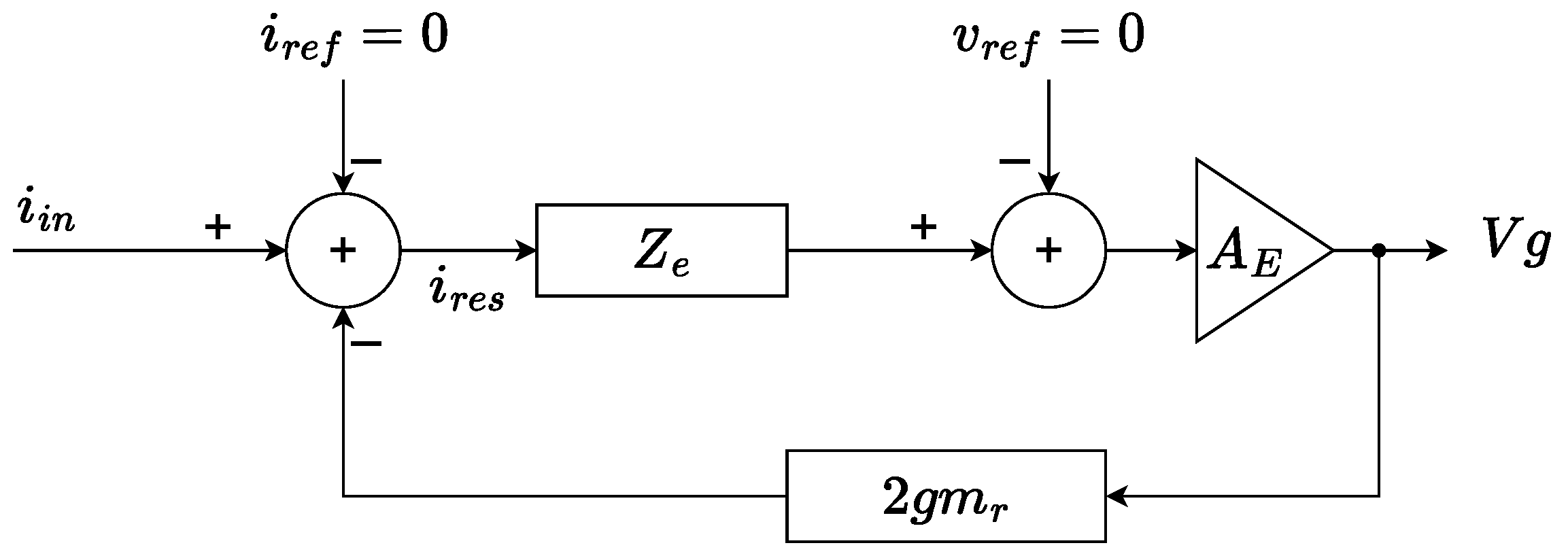
The replica bias loop is schematized in Figure 2, where represents the variation of the current of with respect to its nominal value, is the small-signal component of the reference current (we are assuming an ideal current source ), is the small-signal component of the reference voltage, and is the voltage gain of the auxiliary amplifier:
where is its output conductance, and is the impedance at the output of the replica stage:
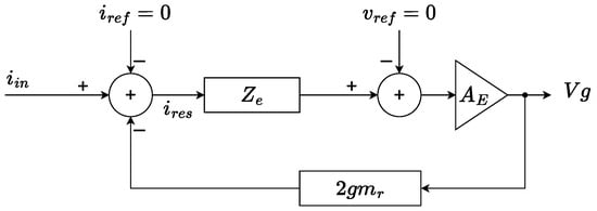
Figure 2.
Block scheme of the replica bias loop.
In the previous equations, standard nomenclature is used for the small-signal parameters of the MOS devices. Subscript r refers to . Subscripts and refer to the PMOS and NMOS devices af the auxiliary error amplifier, and is the output conductance of the current source in the replica stage.
The scheme in Figure 2 enables calculation of the residual current error of the replica stage as
The same error is achieved in the main stage, in the limit of matched drain-source voltages.
Looking at the main amplifier, the voltage generated by the replica loop is applied to the gate terminals of the input devices . The enhanced current mirror load exploits an auxiliary amplifier that sets the drain voltage of (and, by symmetry, of ) to , within the limit of its finite loop gain. The input devices thus present the same gate-source, drain-source, and body-source voltages as their replica counterparts, resulting in robust biasing.
This approach mimics the behavior of a tailed differential pair: within the limit that the replica stage correctly estimates the common-mode current, when a differential input signal is applied, the replica loop keeps the sum of the drain currents of and constant, thus transforming the input stage into a truly differential stage.
2.3. Differential-Mode Analysis
To analyze the small-signal behavior of the proposed amplifier, we can refer to Figure 3, where the capacitances at the different nodes have been explicitly shown.
where and are the input and output capacitances of the auxiliary amplifier, is the output conductance of the first stage, and and are transconductance and output conductance of the second stage. Standard nomenclature is used for the small-signal parameters of the MOS devices. Subscript p refers to , subscript n refers to , and subscripts and refer to NMOS and PMOS devices of the second stage. The same auxiliary amplifier as in the replica stage has been used; hence, is given by (3) (we are neglecting the pole-zero doublet due to the current mirror) and

Figure 3.
Schematic of the amplifier for small-signal analysis.
Let us consider initially the differential-mode transfer function (). The gate terminals of can be assumed at virtual ground; hence, . From Figure 3, the transfer function of the first stage, exploiting the Miller approximation, can be obtained as
where the two pole-zero doublets due to the enhanced current mirror can be neglected, and the transfer function of the second stage is given by
The differential-mode gain is therefore
where the two poles are
For a sufficiently large load capacitance , the dominant pole is given by , and an adequate phase margin is achieved, otherwise some form of compensation is needed. Assuming to be in the large-capacitance case, the gain-bandwidth product (GBW) can be easily calculated as
2.4. Common-Mode Analysis
The common-mode gain of the proposed amplifier is affected both by the enhanced current mirror used for differential to single-ended conversion and by the replica loop. To separately analyze these two effects, we can start analyzing the scheme in Figure 3 in the case of common-mode excitation () with . The analysis yields the common-mode gain of the first stage as
Equation (18) highlights the effect of the enhanced current mirror. We note that is given by the differential mode gain (12) times the reciprocal of the current gain error of the mirror. Using a simple current mirror (with gate and drain of connected together), the current gain error is inversely proportional to gm/gds, whereas in this case the error is scaled down by the gain of the auxiliary amplifier .
The replica bias loop keeps constant the sum of the drain currents of , counteracting the effect of the input common-mode signal. Hence, voltage depends on the input common-mode signal , and the overall common-mode transconductance gain of the pair results lower than the value of used in (18). The effect is similar to a tailed differential pair, where the common-mode input signal sees a source degeneration that reduces the transconductance.
The block scheme in Figure 2 can be used to calculate as a function of , observing that current in Figure 2 is given by . A simple analysis yields
The common-mode transconductance of therefore becomes
and this is the correct value to be used in (18). The overall common-mode gain of the amplifier is thus given by
and CMRR results as
2.5. Noise Analysis
To analyze the noise performance of the proposed OTA, we consider for each transistor in Figure 1 a noise current source that includes a thermal noise component with spectral density
(where is the bias current of the device) and a flicker noise component with spectral density
We calculate the open-circuit output voltage due to the different noise sources, and dividing it by the differential gain (14), we obtain the equivalent input-referred noise voltage.
Noise sources of transistors of the second stage ( and ) are directly connected to the output and yield an output voltage
Neglecting the gain error of the current mirror, the noise sources of the main devices of the first stage ( and ) yield an output voltage
that is the main noise contribution of the OTA. Noise sources in the auxiliary amplifier (devices and ) yield a common-mode contribution that is attenuated by the CMRR. Noise in the replica stage appears at the gates of and is amplified by the common-mode gain (21), resulting in a very small contribution that can be neglected.
2.6. Distortions
To analyze distortions, we model the transconductance gain of the transistors as a power series, limiting it to the third order:
( is the small-signal transconductance , and is ). The differential input signal is assumed to be a pure sinusoidal tone
Analysis of the replica bias loop shows that the gate voltage contains only a second-harmonic component
Applying this signal to the main amplifier, and considering a gain error for the current mirror, the output voltage of the first stage can be calculated as
Equation (32) shows that the use of the CMFF attenuates the second harmonic distortion, which is usually the dominant component in single-ended OTAs.
3. Circuit Design and Simulation
The proposed OTA was designed and simulated using a triple-well 180 nm CMOS technology by TSMC. A 0.3 V supply voltage was adopted, and the amplifier was sized to drive a 200 pF load, rendering it stable without the need of compensation. The design goal was a gain-bandwidth product in the order of 1.5–2 kHz suitable for biomedical and IoT applications and requiring extremely low power consumption. Table 1 reports the sizing of the devices (standard 1.8 V devices of the selected technology) and the bias currents. The design guidelines taken into consideration ensure that the nominal values of and are set to /2. This choice serves to center the dynamic range of each transistor while also enhancing the effectiveness of control amidst PVT variations. The external reference voltage Vref is set to /2.

Table 1.
Transistor sizing.
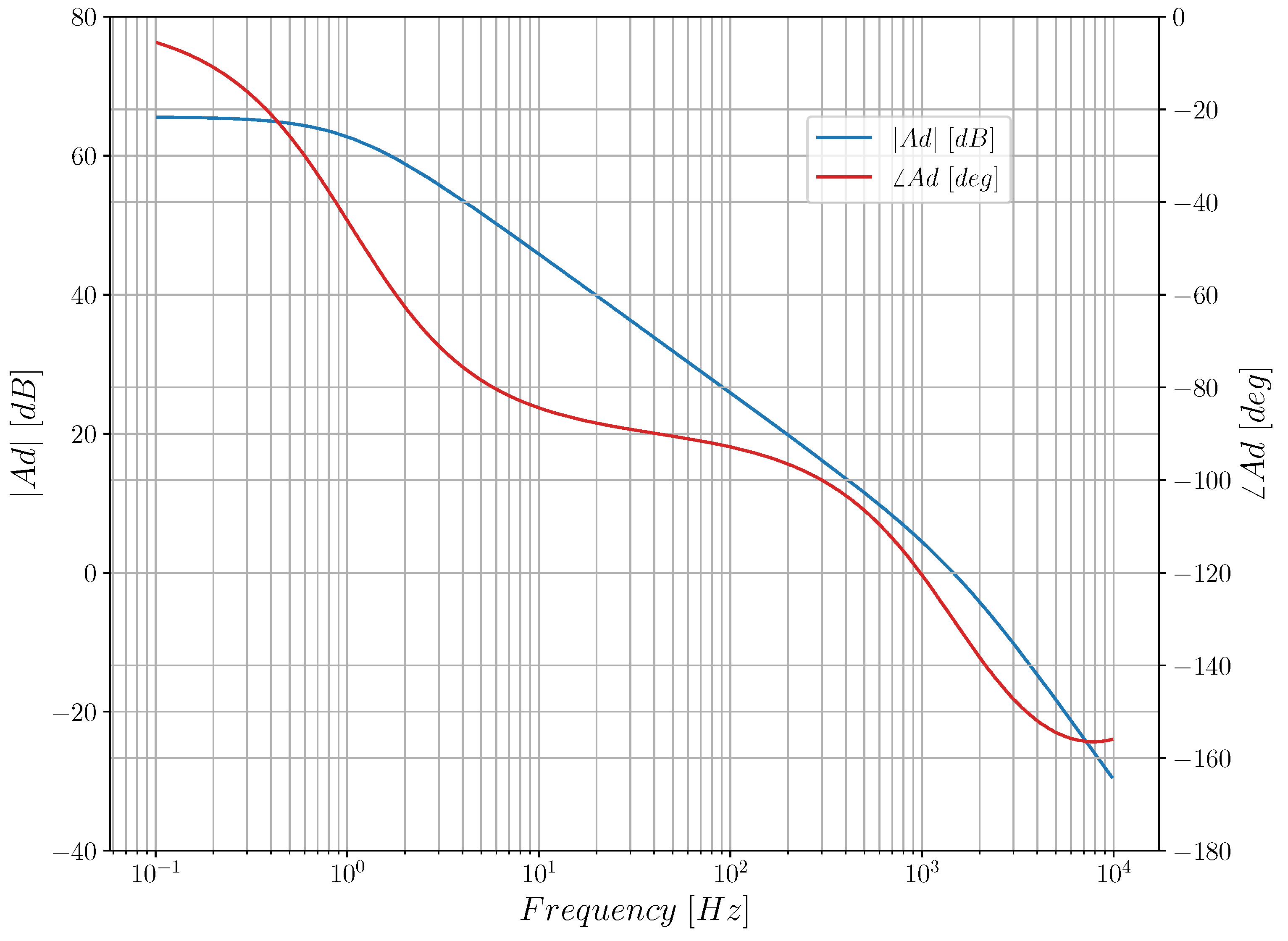
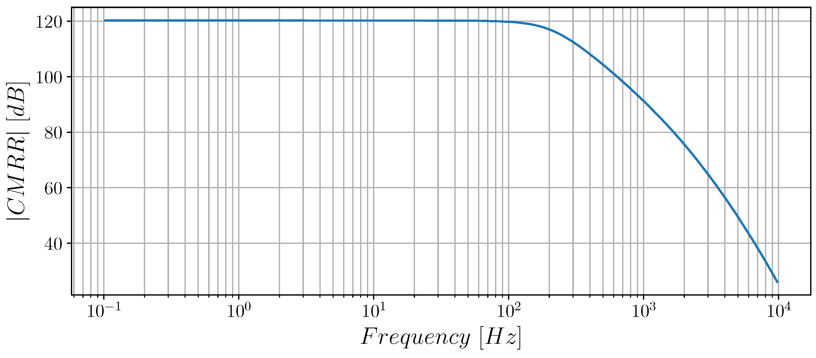
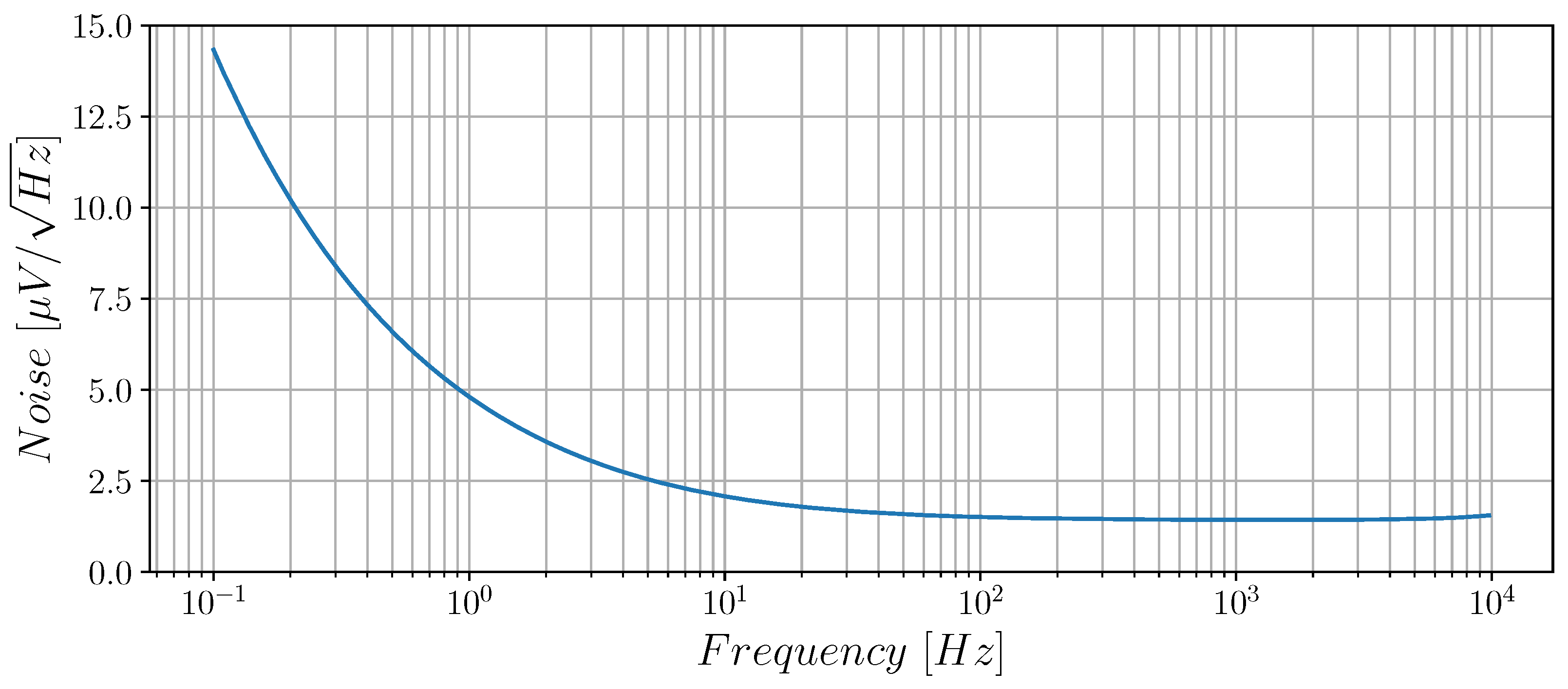
Simulations were performed in the Cadence Virtuoso design environment, considering both nominal conditions and PVT and mismatch variations. The performance of the amplifier under typical conditions (nominal process corner, 27 °C, 0.3 V supply) is reported in Table 2. Figure 4 shows the differential-mode transfer function, highlighting a DC gain of 65.54 dB and a unity-gain bandwidth of about 2 kHz; a phase margin of 50° was achieved. Figure 5 reports the frequency behavior of CMRR, highlighting the extremely good performance that was achieved. Figure 6 shows the input-referred noise (IRN) spectrum, which indicates a white noise level of 1.46 µV/ at 1 kHz and a noise corner frequency of about 800 Hz. Power consumption is 9 nW.
Table 2.
PVT Characterization of the proposed OTA.
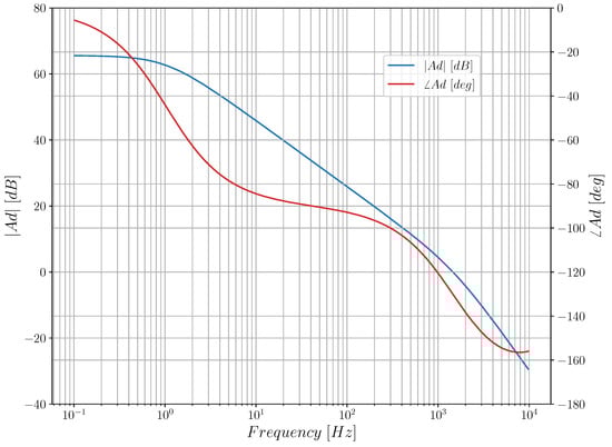
Figure 4.
Differential-mode transfer function.
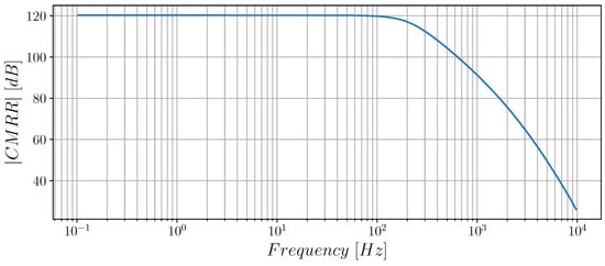
Figure 5.
Common-mode rejection ratio.
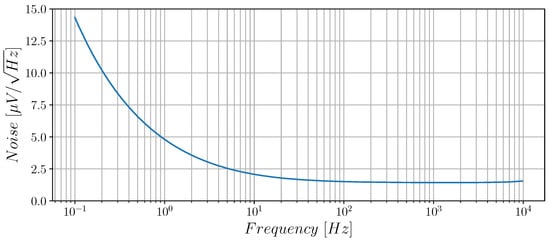
Figure 6.
Input-referred noise spectrum.
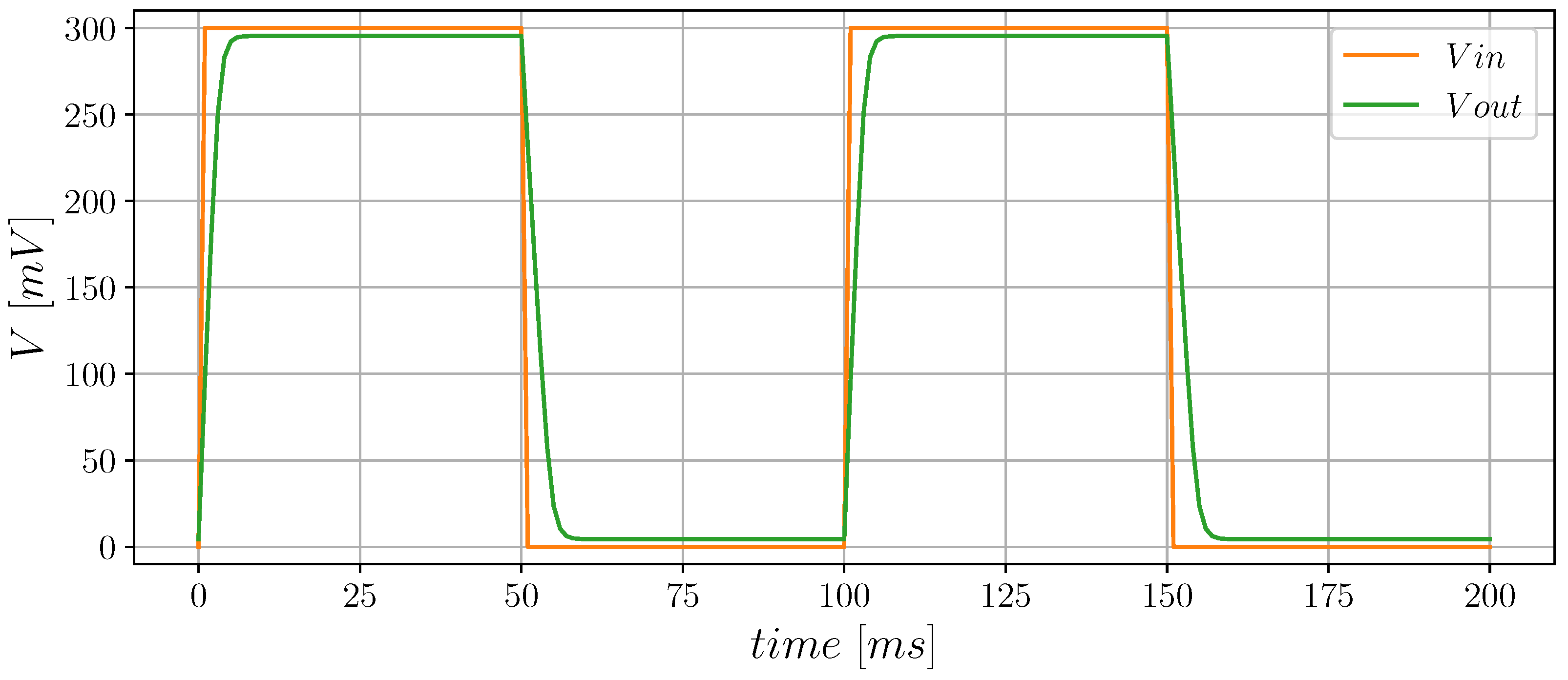
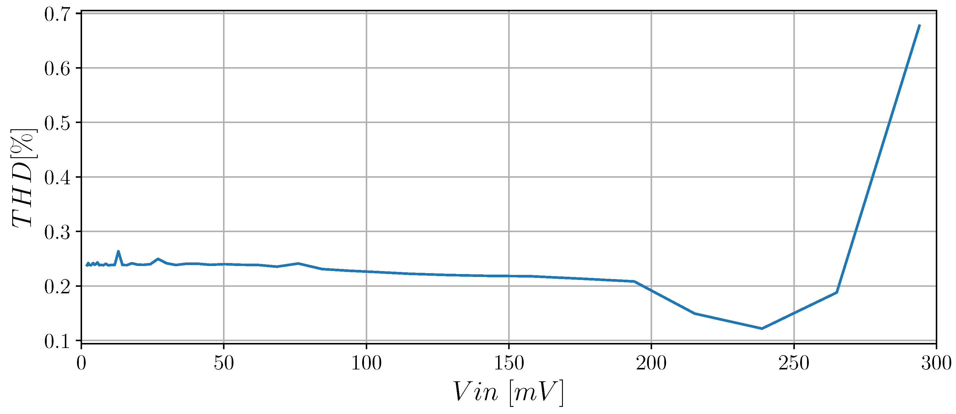
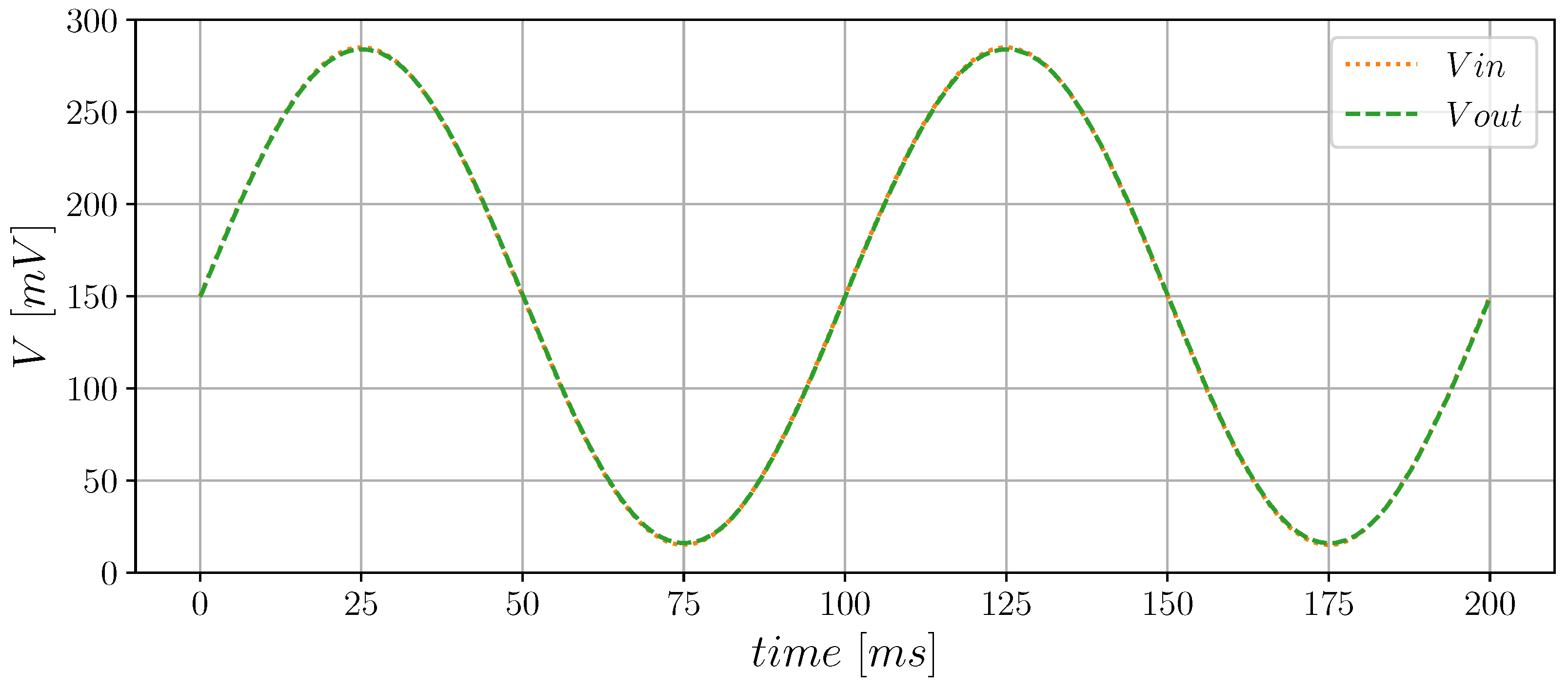
The OTA was also tested in a closed-loop unity-gain configuration. Figure 7 reports the response to a full-swing input voltage step, whereas Figure 8 shows the total harmonic distortion (THD) vs. input signal amplitude when a 10 Hz sinusoidal input signal was applied. Very low distortions were achieved, with a THD as low as 0.24% for a 270 mVpp input (90% of full swing), thanks to the use of the enhanced current mirror and of the replica loop. Figure 9 shows the output signal when a 10 Hz 270 mVpp sine wave was applied.
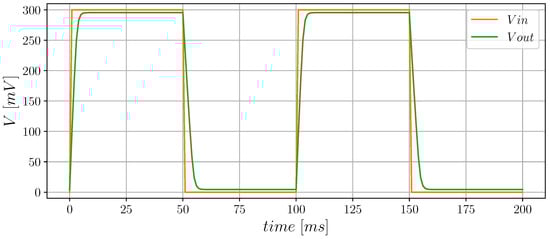
Figure 7.
Step response in unity-gain closed-loop configuration.
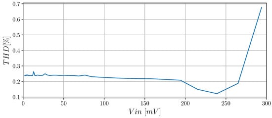
Figure 8.
Total harmonic distortion vs. input peak-to-peak voltage.

Figure 9.
Response of the proposed OTA to a 10 Hz 270 mVpp sinusoidal input signal.
The input common-mode range is rail-to-rail, as can be observed from Figure 10 which reports the input–output DC characteristic when the OTA is closed in a non-inverting buffer configuration.
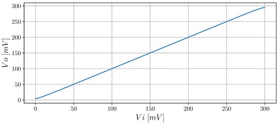
Figure 10.
Input–output DC characteristic in a non-inverting buffer configuration.
Table 2 also reports the effects of variation of process corners, temperature (0 °C and 80 °C), and supply voltage (±10%). Biasing is extremely robust, as evidenced by values of (systematic) offset and power consumption that remain fairly constant, and this reflects on OTA performance. Larger variations are reported for the slew rate, which depends on the second stage, where the proposed bias approach was not applied. The table also includes the input bias current , the value of which remains extremely low under PVT variations, justifying the body-driven approach in this ultra-low voltage environment. Table 3 also shows the combined effect of process and supply/temperature variations, highlighting the good robustness of the proposed approach.
Table 3.
Characterization of the proposed OTA under voltage and temperature variations combined with corners.
The effect of mismatches has also been considered by running 200 Monte Carlo mismatch simulations to evaluate the robustness of the design. A summary of the Monte Carlo simulation results is reported in Table 4, together with the nominal values of the different performances for comparison. Overall, a low offset voltage and robust performance are achieved. Furthermore, linearity performance remains good when mismatches are considered. Mismatches mostly affect the common-mode gain, resulting in a worsening of CMRR and similarly of PSRR. In the presence of mismatches, the common-mode cancellation due to the current mirror load is no longer effective, as is common in all structures of this kind; however, the effect of the replica loop, as shown in (20), remains and provides performance that is still acceptable, similarly to the case of standard tailed differential pairs.
Table 4.
Mismatch Monte Carlo simulations.
Table 5 compares the performance of the proposed OTA with state-of-the-art sub-0.4V results from recent literature. Commonly used figures-of-merit
are calculated and reported to allow a fair comparison. The proposed OTA presents values of , , and noise that compare well to the state-of-the-art, and presents the best results in terms of linearity. The output stage was not optimized for slew rate, resulting in a low value of that is, however, comparable to some of the reported results [30,35,43].
Table 5.
Comparison with state-of-the-art sub-0.4V OTAs.
4. Conclusions
Robust biasing is critical in ULV environments, where tail current generators cannot be used, making it difficult to control the bias current of (pseudo)-differential stages. Moreover, the lack of tail current generators affects CMRR, which relies solely on the cancellation of identical paths and is limited by the gain error of the current mirror. In this paper, we have proposed a biasing approach based on a replica loop and the use of auxiliary amplifiers. The amplifiers provide super-diodes to minimize the gain error of the current mirrors, and the replica loop allows the sum of the currents of the input devices of the OTA to be kept constant against PVT and input common-mode variations. The use of the auxiliary amplifiers maximizes the matching of the drain-source voltages of devices in the main and replica pairs, and allows different values for drain-source and gate-source voltages to be set, optimizing the bias point. Simulations in a 180 nm CMOS technology show high robustness of bias point and performance in the face of PVT variations, high CMRR, though it is still affected by mismatches, and very high linearity. A two-stage OTA provides about 65 dB gain, 2 kHz unity-gain bandwidth on a 200 pF load, 9 nW power consumption, and and noise levels comparable with the state-of-the-art.
Author Contributions
Conceptualization, R.D.S.; methodology, R.D.S., G.S. and F.C.; software, R.D.S.; validation, R.D.S.; formal analysis, R.D.S. and F.C.; investigation, R.D.S., G.S. and F.C.; resources, A.T. and G.S.; data curation, R.D.S.; writing—original draft preparation, R.D.S., G.S. and F.C.; writing—review and editing, R.D.S., G.S. and F.C.; visualization, R.D.S.; supervision, G.S. and A.T.; project administration, G.S. and A.T.; funding acquisition, G.S. and A.T. All authors have read and agreed to the published version of the manuscript.
Funding
This research received no external funding.
Data Availability Statement
The data presented in this study are available in article.
Conflicts of Interest
The authors declare no conflicts of interest.
Abbreviations
The following abbreviations are used in this manuscript:
| ADC | Analog-to-Digital Converter |
| BD | Body-driven |
| CAD | Computer-Aided Design |
| CMFB | Common-Mode Feedback |
| CMFF | Common-Mode Feedforward |
| CMOS | Complementary Metal-Oxide-Semiconductor |
| CMRR | Common-Mode Rejection Ratio |
| D2S | Differential-to-Single-Ended |
| DIBL | Drain-Induced Barrier Lowering |
| DIGOTA | Digital Operational Transconductance Amplifier |
| GBW | Gain-bandwidth product |
| GD | Gate-driven |
| IB | Inverter-based |
| IoT | Internet-of-Things |
| LDO | Low-Dropout Regulator |
| OTA | Operational Transconductance Amplifier |
| PSRR | Power Supply Rejection Ratio |
| PVT | Process, supply voltage and temperature |
| SR | Slew Rate |
| THD | Total Harmonic Distortion |
| ULP | Ultra-Low Power |
| ULV | Ultra-Low Voltage |
| UOPA | Unbuffered Operational Amplifier |
References
- Chandrakasan, A.P.; Verma, N.; Daly, D.C. Ultralow-power electronics for biomedical applications. Annu. Rev. Biomed. Eng. 2008, 10, 247–274. [Google Scholar] [CrossRef] [PubMed]
- Ng, K.A.; Xu, Y.P. A low-power, high CMRR neural amplifier system employing CMOS inverter-based OTAs with CMFB through supply rails. IEEE J. Solid-State Circuits 2016, 51, 724–737. [Google Scholar] [CrossRef]
- Centurelli, F.; Fava, A.; Monsurró, P.; Scotti, G.; Tommasino, P.; Trifiletti, A. Low power switched-resistor band-pass filter for neural recording channels in 130 nm CMOS. Heliyon 2020, 6, e04723. [Google Scholar] [CrossRef] [PubMed]
- Sobin, C.C. A survey on architecture, protocols and challenges in IoT. Wirel. Pers. Commun. 2020, 112, 1383–1429. [Google Scholar] [CrossRef]
- Wardlaw, J.L.; Karaman, I.; Karsilayan, A.İ. Low-power circuits and energy harvesting for structural health monitoring of bridges. IEEE Sens. J. 2013, 13, 709–722. [Google Scholar] [CrossRef]
- Chi, Q.; Yan, H.; Zhang, C.; Pang, Z.; Li, D.X. A reconfigurable smart sensor interface for industrial WSN in IoT environment. IEEE Trans. Ind. Inf. 2014, 10, 1417–1425. [Google Scholar] [CrossRef]
- Harpe, P.; Gao, H.; van Dommele, R.; Cantatore, E.; Van Roermund, A.H.M. A 0.20 mm2 3 nW signal acquisition IC for miniature sensor nodes in 65 nm CMOS. IEEE J. Solid-State Circuits 2016, 51, 240–248. [Google Scholar] [CrossRef]
- Abella, C.S.; Bonina, S.; Cucuccio, A.; D’Angelo, S.; Giustolisi, G.; Grasso, A.D.; Imbruglia, A.; Mauro, G.S.; Nastasi, G.A.M.; Palumbo, G.; et al. Autonomous energy-efficient wireless sensor network platform for home/office automation. IEEE Sens. J. 2019, 19, 3501–3512. [Google Scholar] [CrossRef]
- Carrara, S. Body dust: Well beyond wearable and implantable sensors. IEEE Sens. J. 2021, 21, 12398–12406. [Google Scholar] [CrossRef]
- Aledhari, M.; Razzak, R.; Qolomany, B.; Al-Fuqaha, A.; Saeed, F. Biomedical IoT: Enabling technologies, architectural elements, challenges, and future directions. IEEE Access 2022, 10, 31306–31339. [Google Scholar] [CrossRef]
- Bock, D.C.; Marschilok, A.C.; Takeuchi, K.J.; Takeuchi, E.S. Batteries used to power implantable biomedical devices. Electrochim. Acta 2012, 84, 155–164. [Google Scholar] [CrossRef] [PubMed]
- Elahi, H.; Munir, K.; Eugeni, M.; Atek, S.; Gaudenzi, P. Energy harvesting towards self-powered IoT devices. Energies 2020, 13, 5528. [Google Scholar] [CrossRef]
- Grossi, M. Energy harvesting strategies for wireless sensor networks and mobile devices: A review. Electronics 2021, 10, 661. [Google Scholar] [CrossRef]
- Sanislav, T.; Mois, G.D.; Zeadally, S.; Folea, S.C. Energy harvesting techniques for Internet of Things (IoT). IEEE Access 2021, 9, 39530–39549. [Google Scholar] [CrossRef]
- Lin, C.Y.; Chen, W.L.; Ker, M.D. Implantable stimulator for epileptic seizure suppression with loading impedance adaptability. IEEE Trans. Biomed. Circuits Syst. 2013, 7, 196–203. [Google Scholar] [CrossRef] [PubMed]
- Hannan, M.A.; Mutashar, S.; Samad, S.A.; Hussain, A. Energy harvesting for the implantable biomedical devices: Issues and challenges. Biomed. Eng. Online 2014, 13, 79. [Google Scholar] [CrossRef] [PubMed]
- Wu, T.; Redouté, J.M.; Yuce, M.R. A wireless implantable sensor design with subcutaneous energy harvesting for long-term IoT healthcare applications. IEEE Access 2018, 6, 35801–35808. [Google Scholar] [CrossRef]
- Khateb, F.; Dabbous, S.B.A.; Vlassis, S. A survey of non-conventional techniques for low-voltage low-power analog circuit design. Radioengineering 2013, 22, 415–427. [Google Scholar]
- Toledo, P.; Rubino, R.; Musolino, F.; Crovetti, P. Re-thinking analog integrated circuits in digital terms: A new design concept for the IoT era. IEEE Trans. Circuits Syst. II 2021, 68, 816–822. [Google Scholar] [CrossRef]
- Richelli, A.; Colalongo, L.; Kovacs-Vajna, Z.; Calvetti, G.; Ferrari, D.; Finanzini, M.; Pinetti, S.; Prevosti, E.; Savoldelli, J.; Scarlassara, S. A survey of low voltage and low power amplifier topologies. J. Low Power Electron. Appl. 2018, 8, 22. [Google Scholar] [CrossRef]
- Grasso, A.D.; Pennisi, S. Ultra-low power amplifiers for IoT nodes. In Proceedings of the 2018 25th IEEE International Conference on Electronics, Circuits and Systems (ICECS), Bordeaux, France, 9–12 December 2018; pp. 497–500. [Google Scholar] [CrossRef]
- Toledo, P.; Crovetti, P.; Aiello, O.; Alioto, M. Design of digital OTAs with operation down to 0.3 V and nW power for direct harvesting. IEEE Trans. Circuits Syst. I 2021, 68, 3693–3706. [Google Scholar] [CrossRef]
- Richelli, A.; Faustini, P.; Rosa, A.; Colalongo, L. An investigation of the operating principles and power consumption of digital-based analog amplifiers. J. Low Power Electron. Appl. 2023, 13, 51. [Google Scholar] [CrossRef]
- Privitera, M.; Crovetti, P.; Grasso, A.D. A novel digital OTA topology with 66-dB DC gain and 12.3-kHz bandwidth. IEEE Trans. Circuits Syst. II 2023, 70, 3988–3992. [Google Scholar] [CrossRef]
- Drost, B.; Talegaonkar, M.; Hanumolu, P.K. Analog filter design using ring oscillator integrators. IEEE J. Solid-State Circuits 2012, 47, 3120–3129. [Google Scholar] [CrossRef]
- Kalani, S.; Haque, T.; Gupta, R.; Kinget, P.R. Benefits of using VCO-OTAs to construct TIAs in wideband current-mode receivers over inverter-based OTAs. IEEE Trans. Circuits Syst. I 2019, 66, 1681–1691. [Google Scholar] [CrossRef]
- Chatterjee, S.; Tsividis, Y.; Kinget, P. 0.5-V analog circuit techniques and their application in OTA and filter design. IEEE J. Solid-State Circuits 2005, 40, 2373–2387. [Google Scholar] [CrossRef]
- Ferreira, L.H.C.; Sonkusale, S.R. A 60-dB gain OTA operating at 0.25-V power supply in 130-nm digital CMOS process. IEEE Trans. Circuits Syst. I 2014, 61, 1609–1617. [Google Scholar] [CrossRef]
- Abdelfattah, O.; Roberts, G.W.; Shih, I.; Shih, Y.C. An ultra-low-voltage CMOS process-insensitive self-biased OTA with rail-to-rail input range. IEEE Trans. Circuits Syst. I 2015, 62, 2380–2390. [Google Scholar] [CrossRef]
- Akbari, M.; Hashemipour, O. A 63-dB gain OTA operating in subthreshold with 20-nW power consumption. Int. J. Circuit Theory Appl. 2017, 45, 843–850. [Google Scholar] [CrossRef]
- Kulej, T.; Khateb, F. Design and implementation of sub 0.5-V OTAs in 0.18-μm CMOS. Int. J. Circuit Theory Appl. 2018, 46, 1129–1143. [Google Scholar] [CrossRef]
- Wen, B.; Zhang, Q.; Zhao, X. A two-stage CMOS OTA with enhanced transconductance and DC-gain. Analog Integr. Circuits Sig. Process. 2019, 98, 257–264. [Google Scholar] [CrossRef]
- Kulej, T.; Khateb, F. A compact 0.3-V class AB bulk-driven OTA. IEEE Trans. Very Large Scale Integr. VLSI Syst. 2020, 28, 224–232. [Google Scholar] [CrossRef]
- Kulej, T.; Khateb, F. A 0.3-V 98-dB rail-to-rail OTA in 0.18 μm CMOS. IEEE Access 2020, 8, 27459–27467. [Google Scholar] [CrossRef]
- Woo, K.C.; Yang, B.D. A 0.25-V rail-to-rail three-stage OTA with an enhanced DC gain. IEEE Trans. Circuits Syst. II 2020, 67, 1179–1183. [Google Scholar] [CrossRef]
- Deo, N.; Sharan, T.; Dubey, T. Subthreshold biased enhanced bulk-driven double recycling current mirror OTA. Analog Integr. Circuits Sig. Process. 2020, 105, 229–242. [Google Scholar] [CrossRef]
- Wang, Y.; Zhang, Q.; Zhao, X.; Dong, L. An enhanced bulk-driven OTA with high transconductance against CMOS scaling. AEU Int. J. Electron. Commun. 2021, 130, 153581. [Google Scholar] [CrossRef]
- Centurelli, F.; Della Sala, R.; Scotti, G.; Trifiletti, A. A 0.3 V, rail-to-rail, ultralow-power, non-tailed, body-driven, sub-threshold amplifier. Appl. Sci. 2021, 11, 2528. [Google Scholar] [CrossRef]
- Centurelli, F.; Della Sala, R.; Monsurró, P.; Scotti, G.; Trifiletti, A. A tree-based architecture for high-performance ultra-low-voltage amplifiers. J. Low Power Electron. Appl. 2022, 12, 12. [Google Scholar] [CrossRef]
- Centurelli, F.; Della Sala, R.; Monsurró, P.; Tommasino, P.; Trifiletti, A. An ultra-low-voltage class-AB OTA exploiting local CMFB and body-to-gate interface. AEU Int. J. Electron. Commun. 2022, 145, 154081. [Google Scholar] [CrossRef]
- Dong, S.; Wang, W.; Tong, X. A 0.25-V 90 dB PVT-stabilized four-stage OTA withmidrulear Q-factor modulation and fast slew-rate enhancement for ultra-low supply ADCs. AEU Int. J. Electron. Commun. 2022, 144, 154044. [Google Scholar] [CrossRef]
- Ballo, A.; Grasso, A.D.; Pennisi, S. 0.4-V, 81.3-nA bulk-driven single-stage CMOS OTA with enhanced transconductance. Electronics 2022, 11, 2704. [Google Scholar] [CrossRef]
- Della Sala, R.; Centurelli, F.; Scotti, G.; Tommasino, P.; Trifiletti, A. A differential-to-single-ended converter based on enhanced body-driven current mirrors targeting ultra-low-voltage OTAs. Electronics 2022, 11, 3838. [Google Scholar] [CrossRef]
- Della Sala, R.; Centurelli, F.; Monsurrò, P.; Scotti, G.; Trifiletti, A. A 0.3V rail-to-rail three-stage OTA with high DC gain and improved robustness to PVT variations. IEEE Access 2023, 11, 19635–19644. [Google Scholar] [CrossRef]
- Ballo, A.; Grasso, A.D.D.; Pennisi, S.; Susinni, G. A 0.3-V 8.5-μ a bulk-driven OTA. IEEE Trans. Very Large Scale Integr. VLSI Syst. 2023, 31, 1444–1448. [Google Scholar] [CrossRef]
- Miguel, J.M.A.; Lopez-Martin, A.J.; Acosta, L.; Ramirez-Angulo, J.; Carvajal, R.G. Using floating gate and quasi-floating gate techniques for rail-to-rail tunable CMOS transconductor design. IEEE Trans. Circuits Syst. I 2011, 58, 1604–1614. [Google Scholar] [CrossRef]
- Khateb, F. Bulk-driven floating-gate and bulk-driven quasi-floating-gate techniques for low-voltage low-power analog circuits design. AEU Int. J. Electron. Commun. 2014, 68, 64–72. [Google Scholar] [CrossRef]
- Braga, R.A.S.; Ferreira, L.H.C.; Coletta, G.D.; Dutra, O.O. A 0.25-V calibration-less inverter-based OTA for low-frequency Gm-C applications. Microelectron. J. 2019, 83, 62–72. [Google Scholar] [CrossRef]
- Lv, L.; Zhou, X.; Qiao, Z.; Li, Q. Inverter-based subthreshold amplifier techniques and their application in 0.3-V ΔΣ-modulators. IEEE J. Solid-State Circuits 2019, 54, 1436–1445. [Google Scholar] [CrossRef]
- Manfredini, G.; Catania, A.; Benvenuti, L.; Cicalini, M.; Piotto, M.; Bruschi, P. Ultra-low-voltage inverter-based amplifier with novel common-mode stabilization loop. Electronics 2020, 9, 1019. [Google Scholar] [CrossRef]
- Rodovalho, L.H.; Aiello, O.; Rodrigues, C.R. Ultra-low-voltage inverter-based operational transconductance amplifiers with voltage gain enhancement by improved composite transistors. Electronics 2020, 9, 1410. [Google Scholar] [CrossRef]
- Liu, Y.; Zhang, B.; Cheng, X.; Han, J.; Zeng, X. A 0.9V all digital synthesizable OPAMP with boosted gain and widened common mode input range. In Proceedings of the 2020 IEEE 15th International Conference on Solid-State & Integrated Circuit Technology (ICSICT), Kunming, China, 3–6 November 2020; pp. 1–3. [Google Scholar] [CrossRef]
- Della Sala, R.; Centurelli, F.; Scotti, G. A novel differential to single-ended converter for ultra-low-voltage inverter-based OTAs. IEEE Access 2022, 10, 98179–98190. [Google Scholar] [CrossRef]
- Della Sala, R.; Centurelli, F.; Scotti, G. Enabling ULV fully synthesizable analog circuits: The BA cell, a standard-cell-based building block for analog design. IEEE Trans. Circuits Syst. II 2022, 69, 4689–4693. [Google Scholar] [CrossRef]
- Della Sala, R.; Centurelli, F.; Scotti, G. A high performance 0.3 V standard-cell-based OTA suitable for automatic layout flow. Appl. Sci. 2023, 13, 5517. [Google Scholar] [CrossRef]
- Fonderie, J.; Maris, M.M.; Schnitger, E.J.; Huijsing, J.H. 1-V operational amplifier with rail-to-rail input and output ranges. IEEE J. Solid-State Circuits 1989, 24, 1551–1559. [Google Scholar] [CrossRef]
- Mohieldin, A.N.; Sanchez-Sinencio, E.; Silva-Martinez, J. A fully balanced pseudo-differential OTA with common-mode feedforward and inherent common-mode feedback detector. IEEE J. Solid-State Circuits 2003, 38, 663–668. [Google Scholar] [CrossRef]
- Wang, J.; Li, Y.; Zhu, Z. A 0.6-V pseudo-differential OTA with switched-opamp technique for low power applications. Microelectron. J. 2019, 90, 117–122. [Google Scholar] [CrossRef]
- Ghosh, S.; Bhadauria, V. An ultra-low-power near rail-to-rail pseudo-differential subthreshold gate-driven OTA with improved small and large signal performances. Analog Integr. Circuits Sig. Process. 2021, 109, 345–366. [Google Scholar] [CrossRef]


Disclaimer/Publisher’s Note: The statements, opinions and data contained in all publications are solely those of the individual author(s) and contributor(s) and not of MDPI and/or the editor(s). MDPI and/or the editor(s) disclaim responsibility for any injury to people or property resulting from any ideas, methods, instructions or products referred to in the content. |
© 2024 by the authors. Licensee MDPI, Basel, Switzerland. This article is an open access article distributed under the terms and conditions of the Creative Commons Attribution (CC BY) license (https://creativecommons.org/licenses/by/4.0/).