
A Low Power Injection-Locked CDR Using 28 nm FDSOI Technology for Burst-Mode Applications

Abstract
1. Introduction
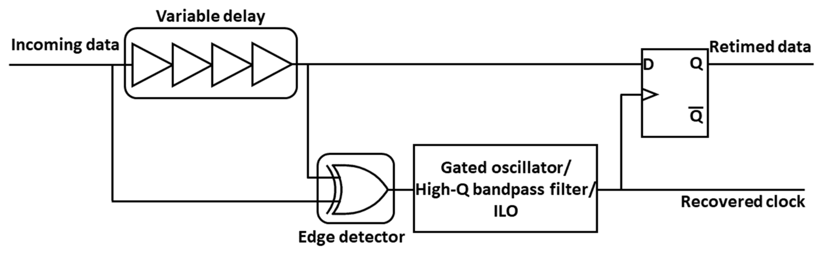
2. CDR Architectures
3. Injection Complementary QRO
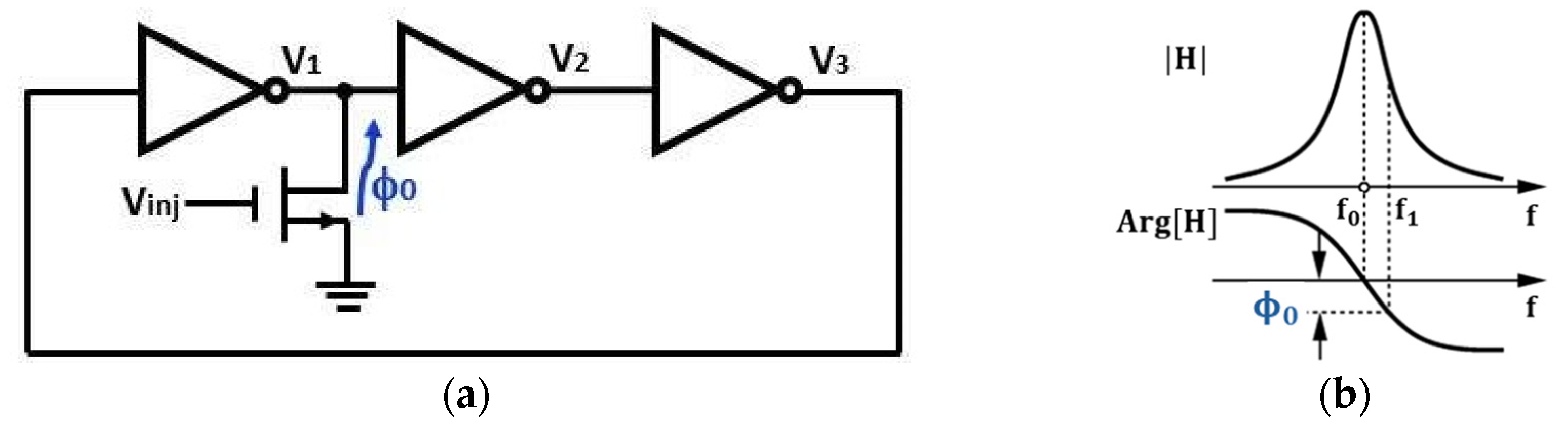
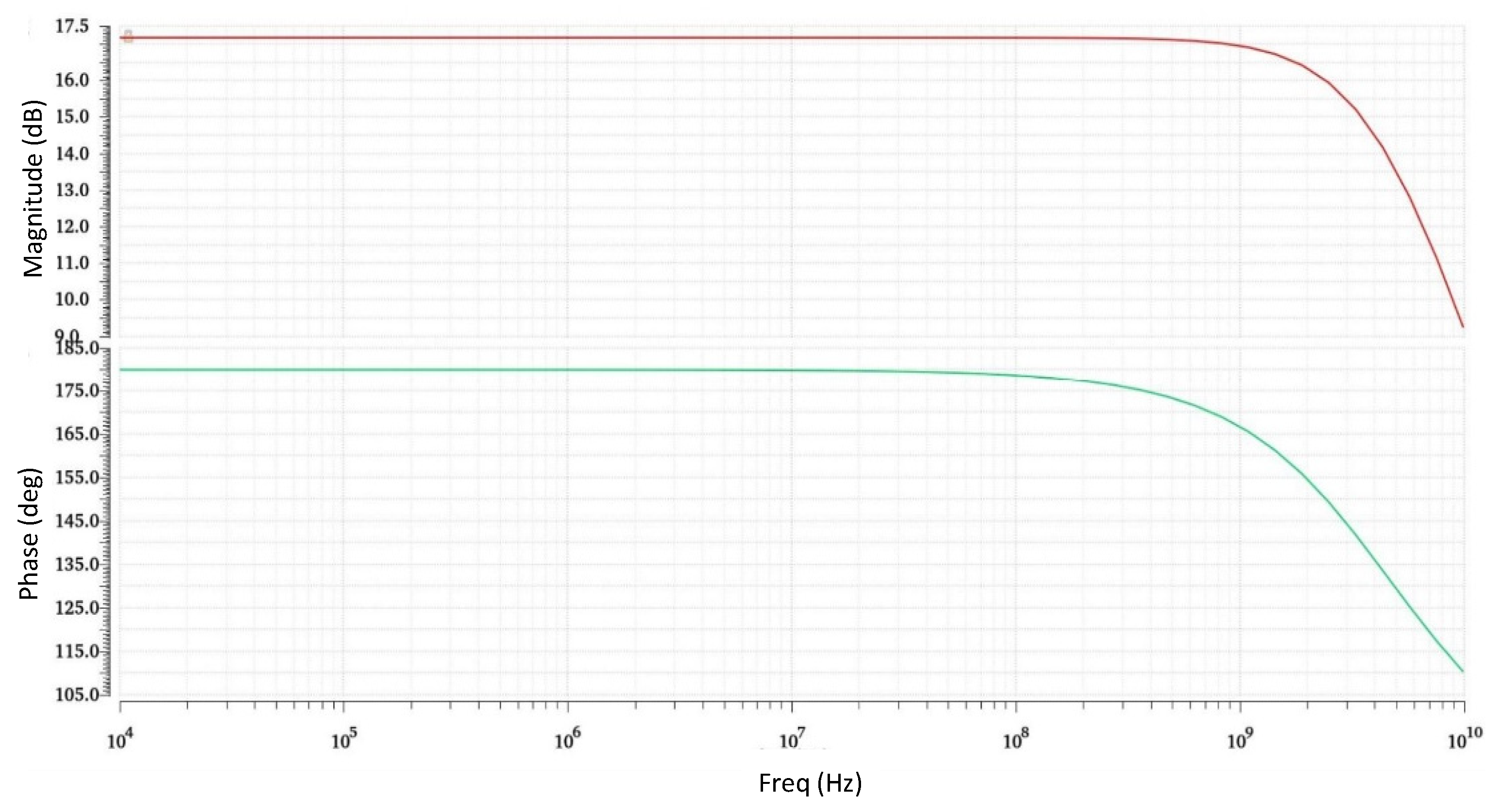
3.1. RO Design
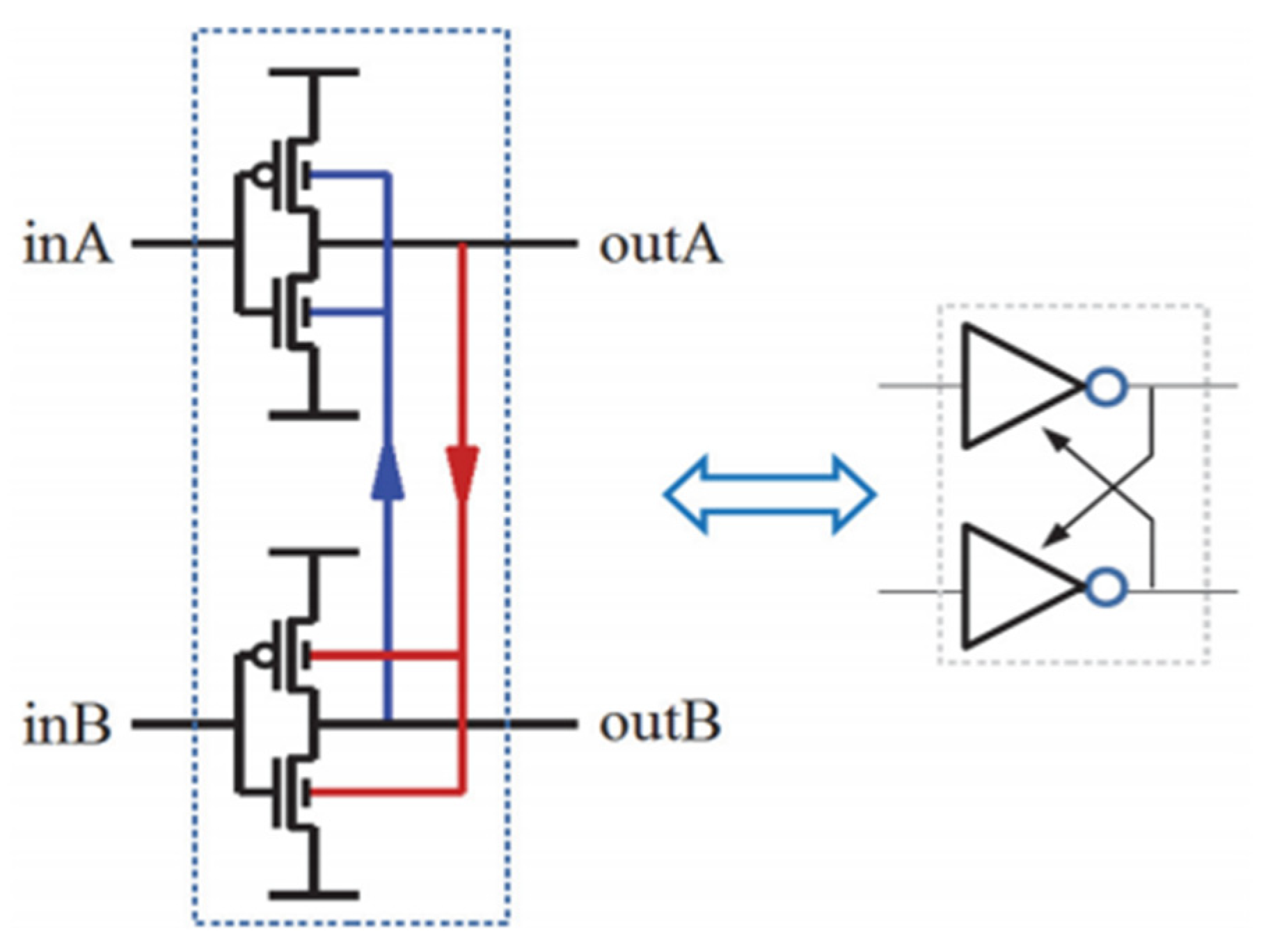
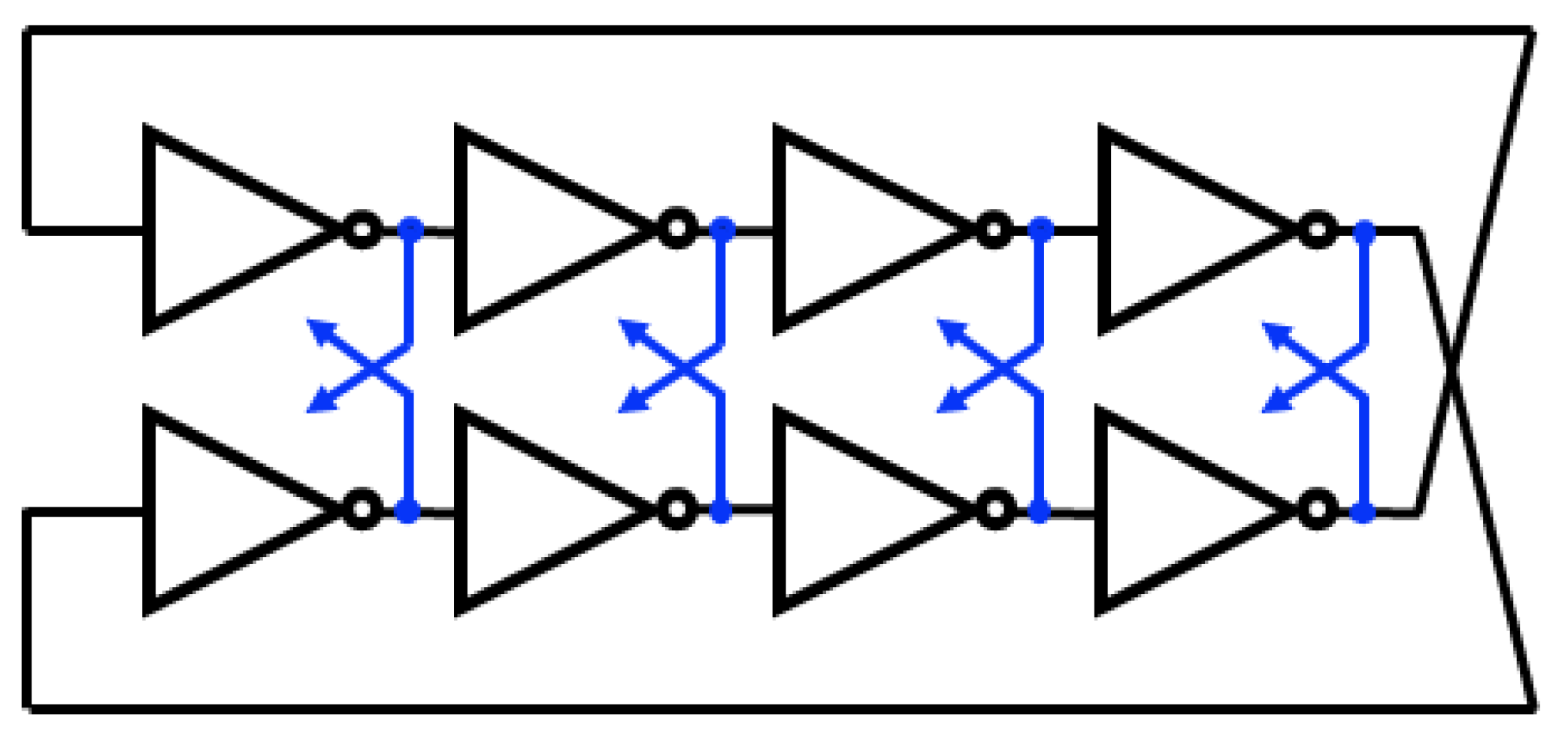
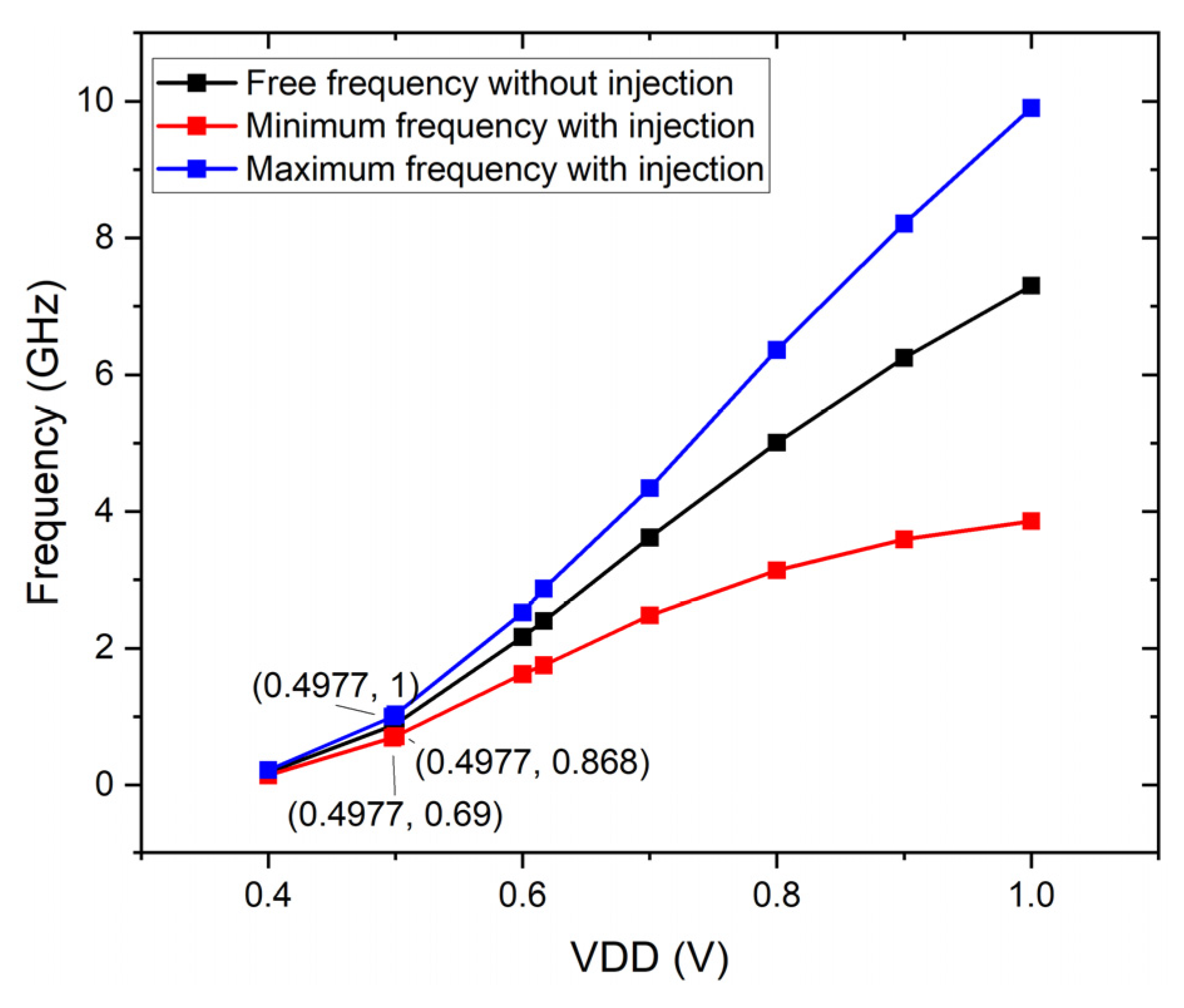
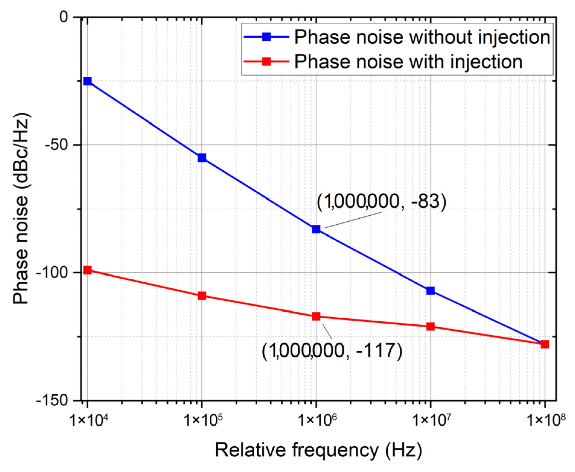
3.2. Injection Complementary QRO
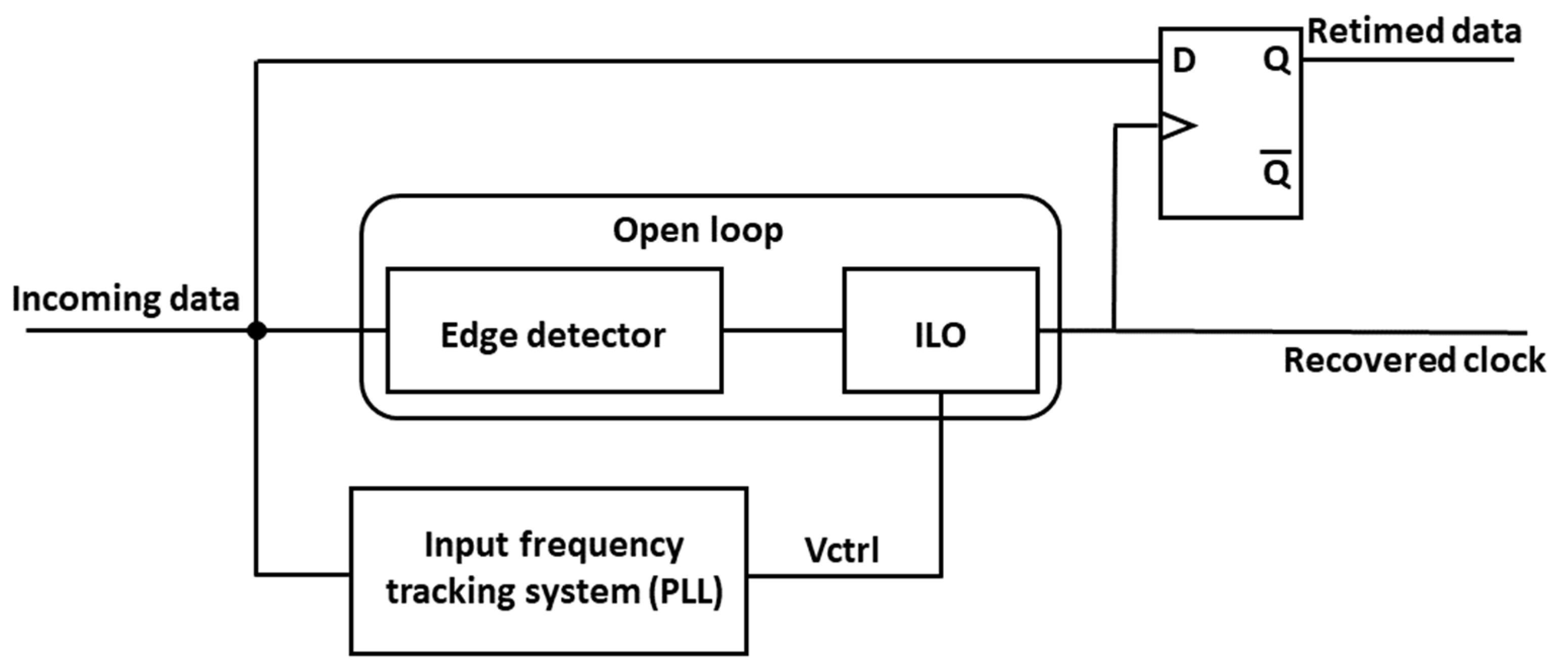
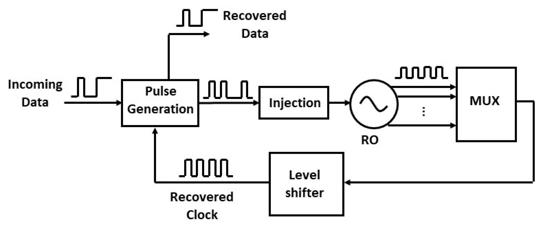
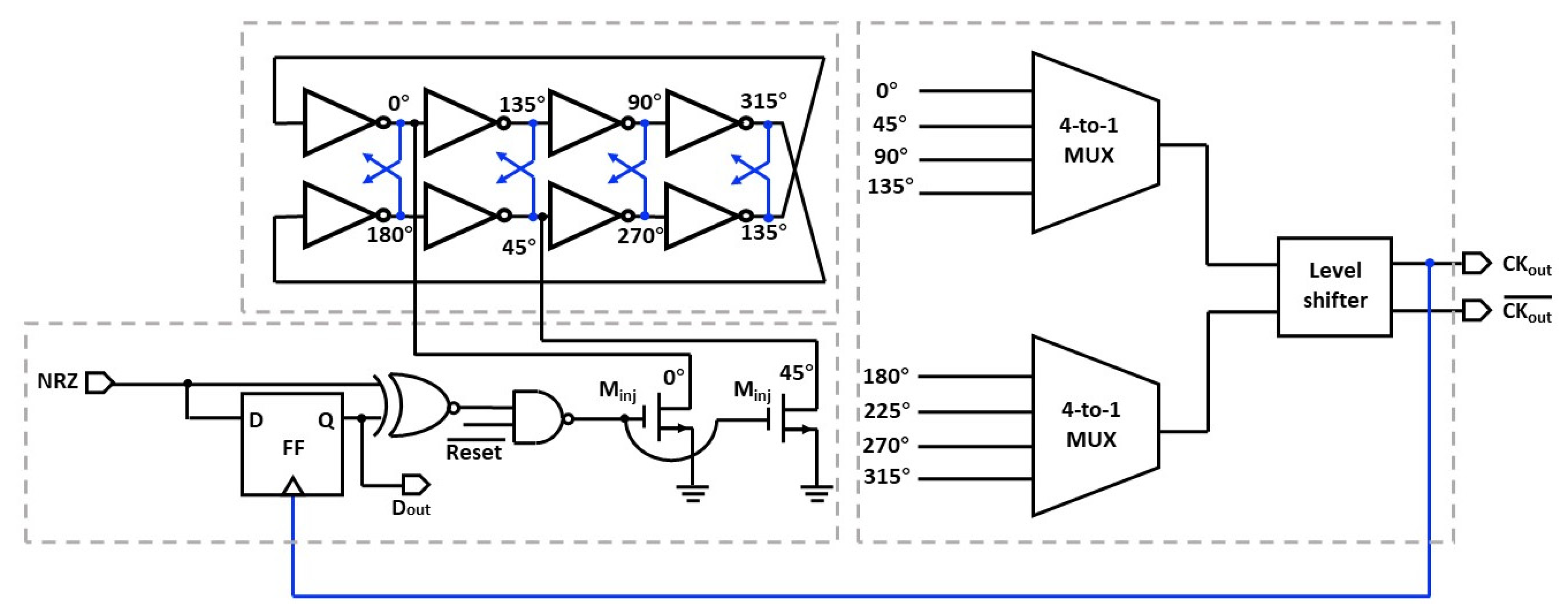
4. Proposed ILCDR
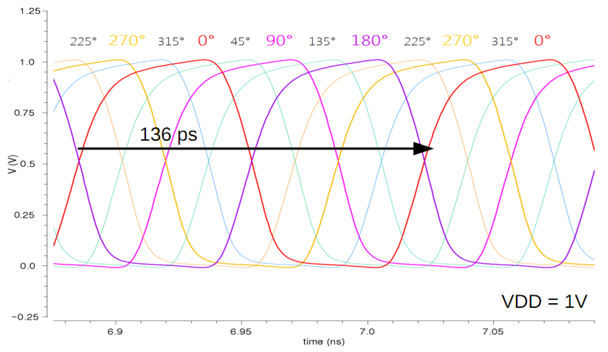
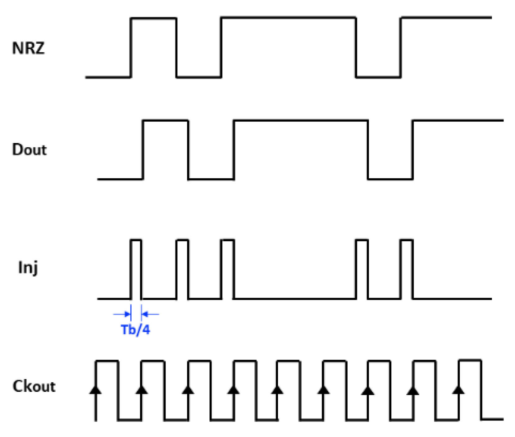
4.1. Timing Analysis of the Proposed ILCDR
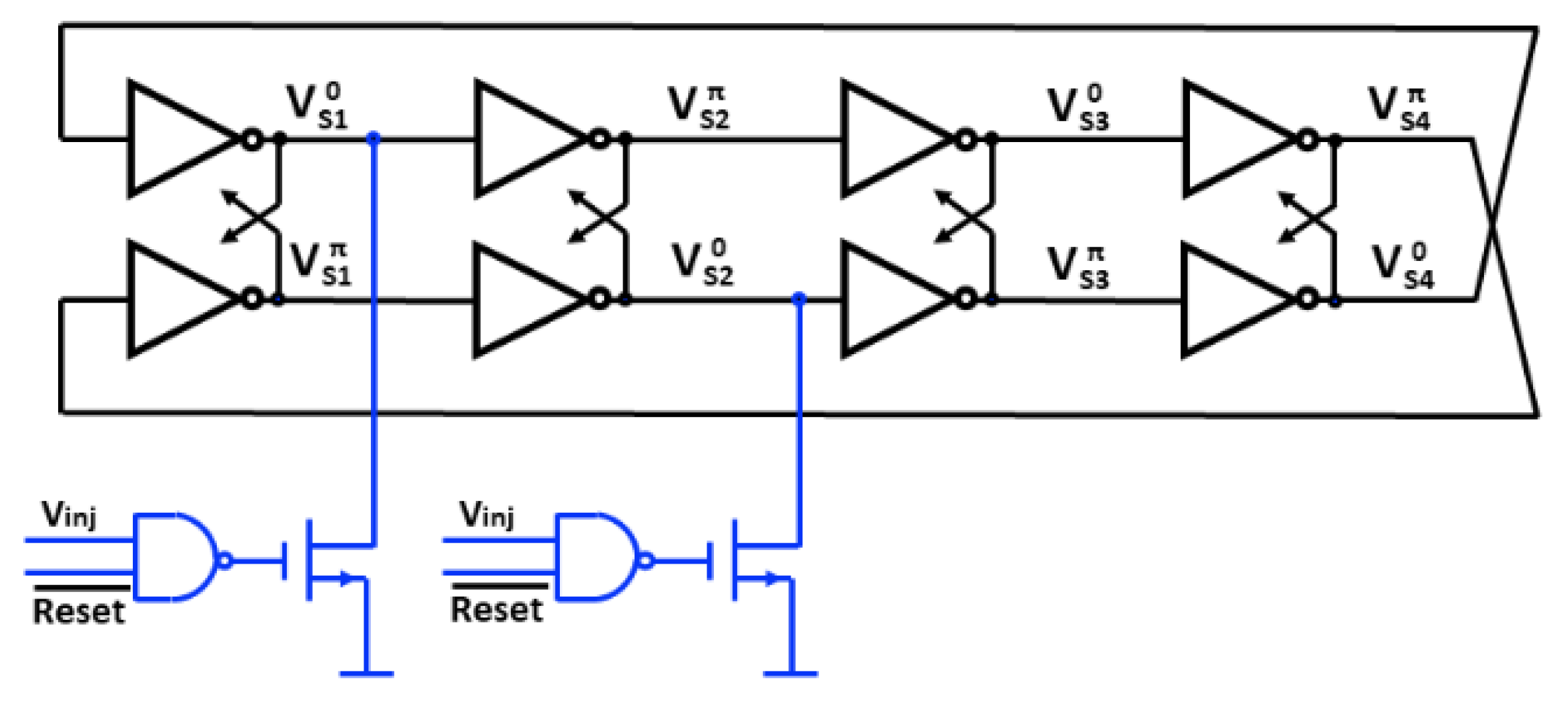
4.2. Architecture
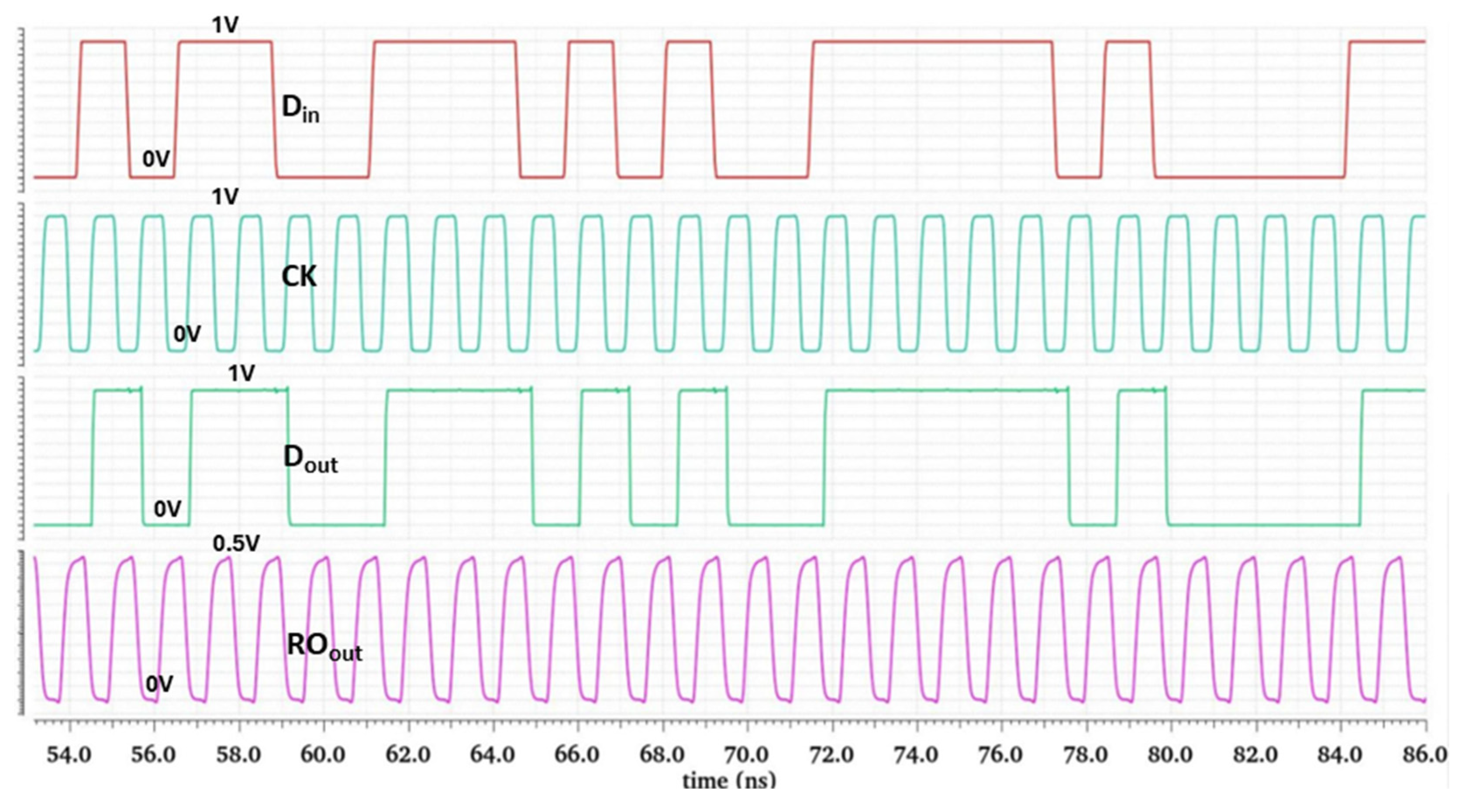
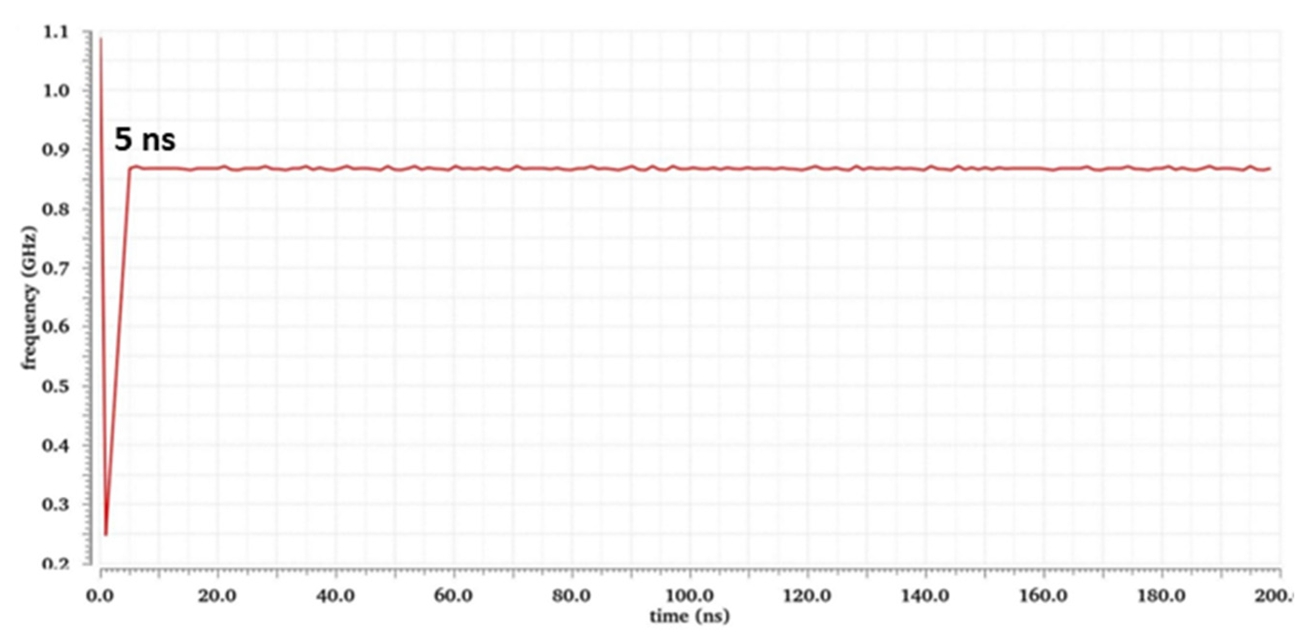
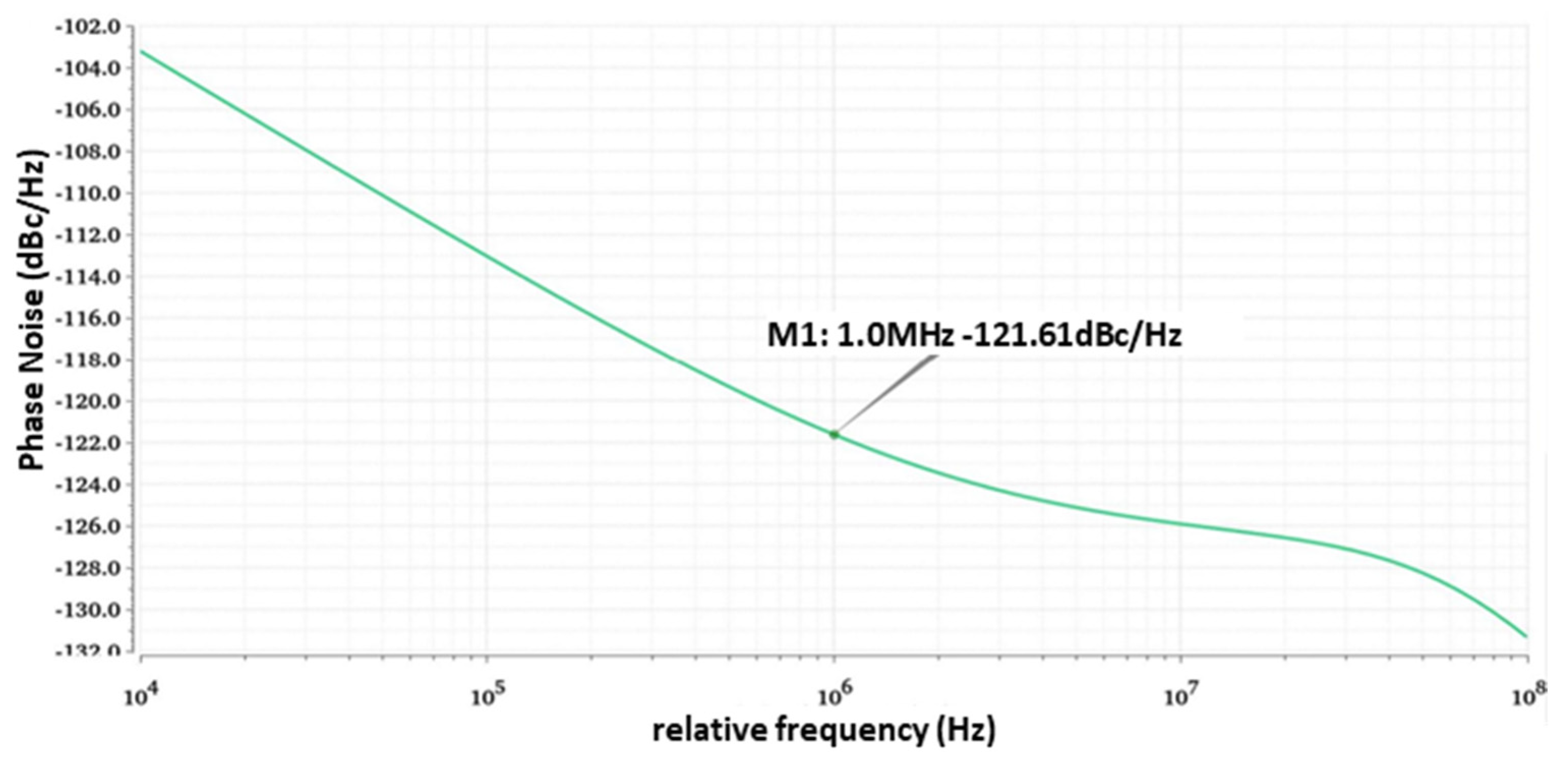
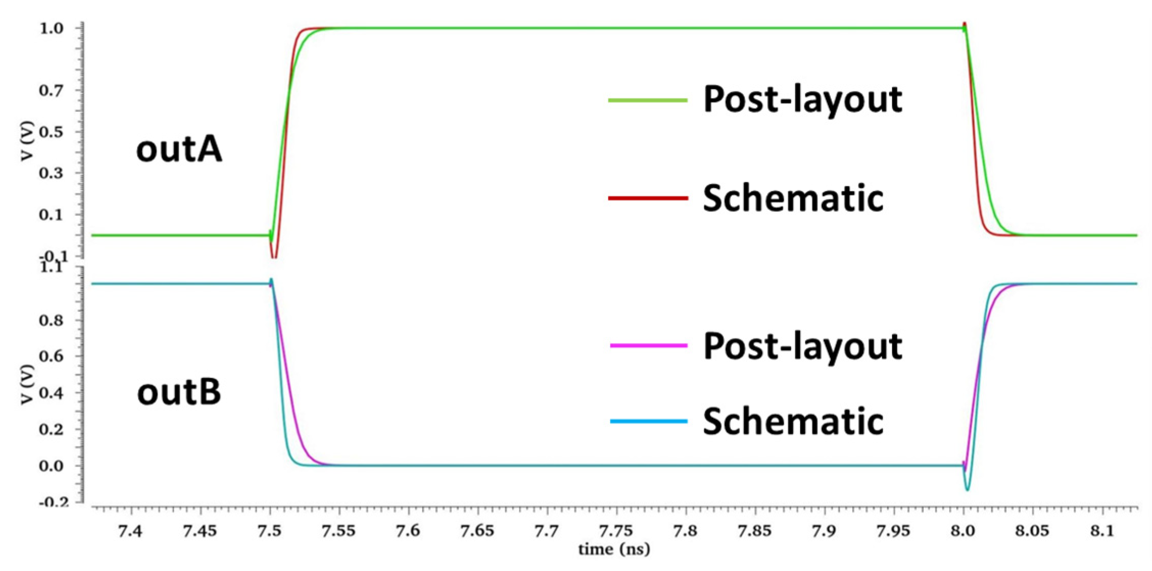
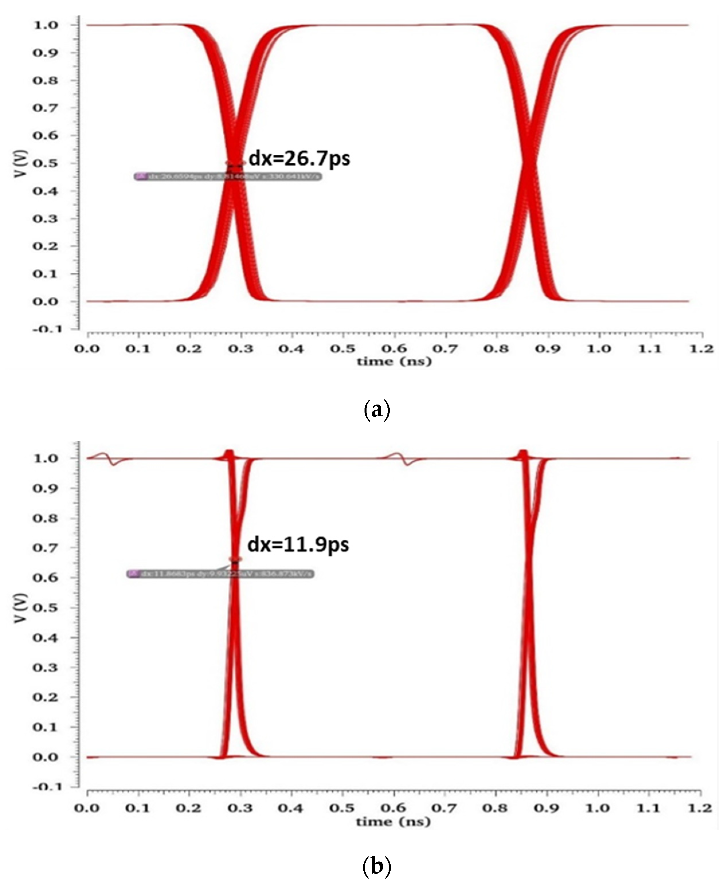
4.3. Schematic Simulation Results
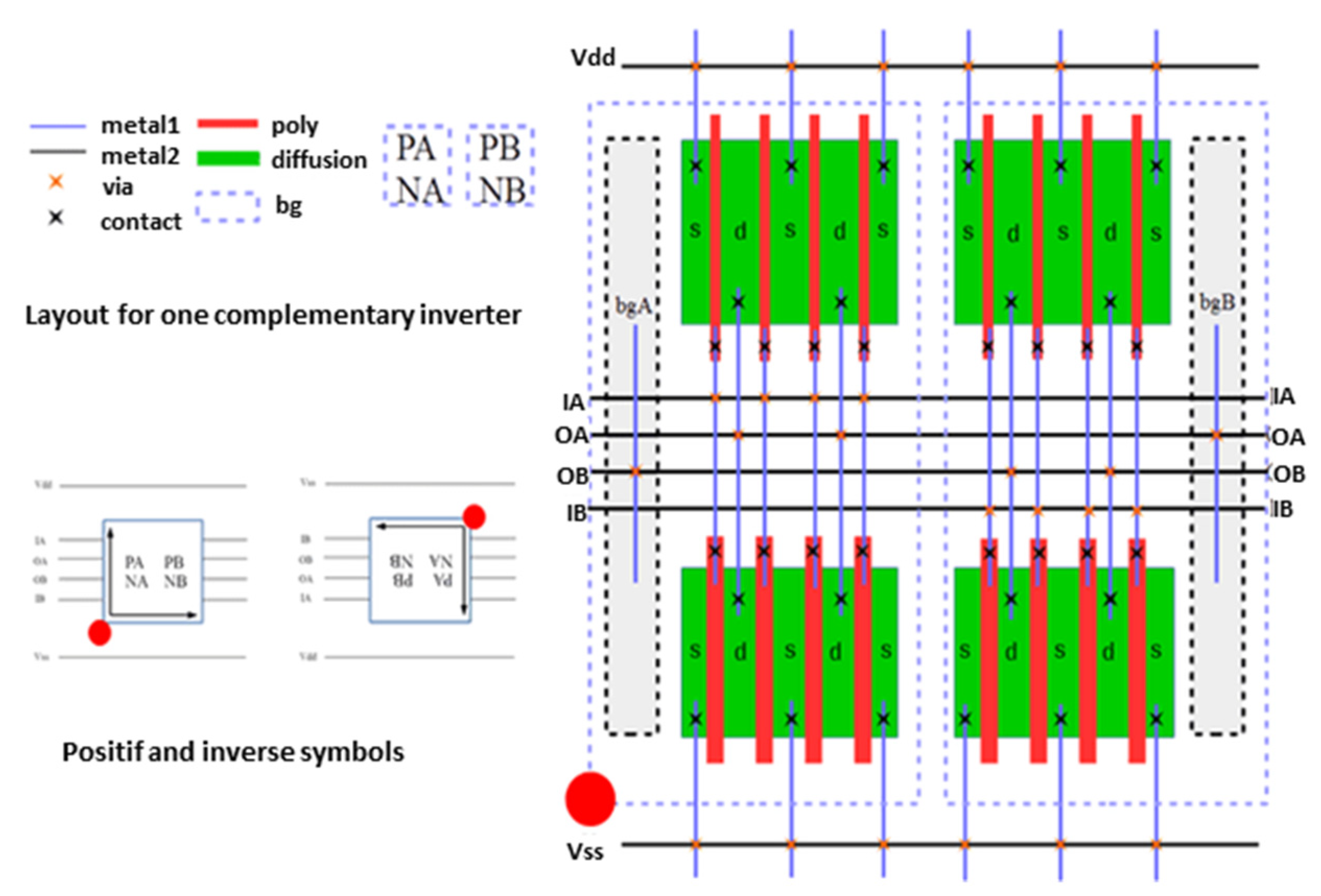
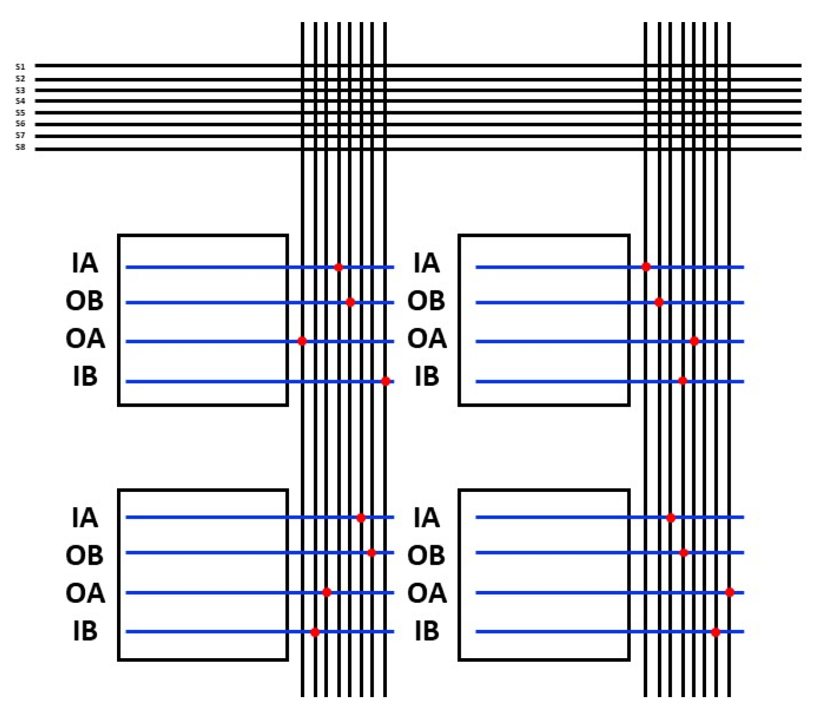
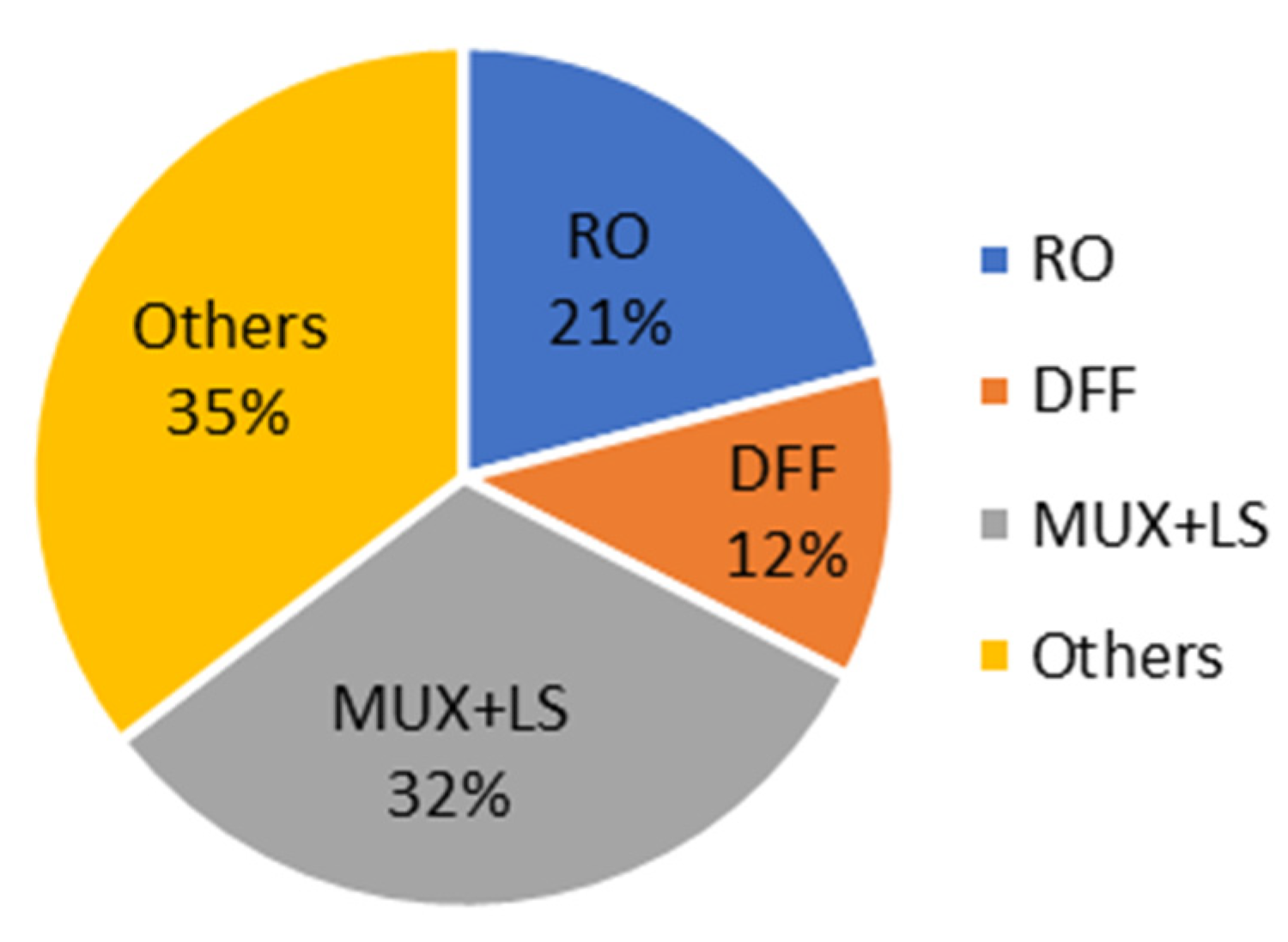
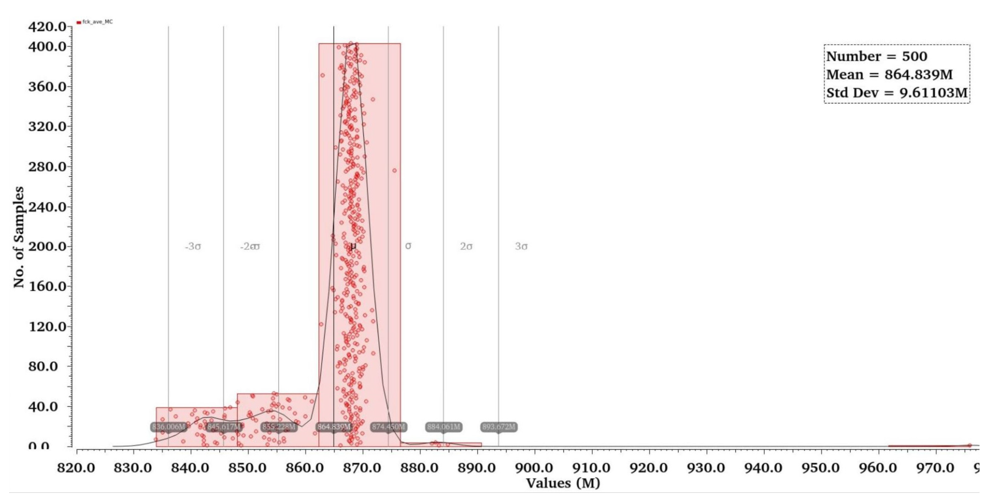
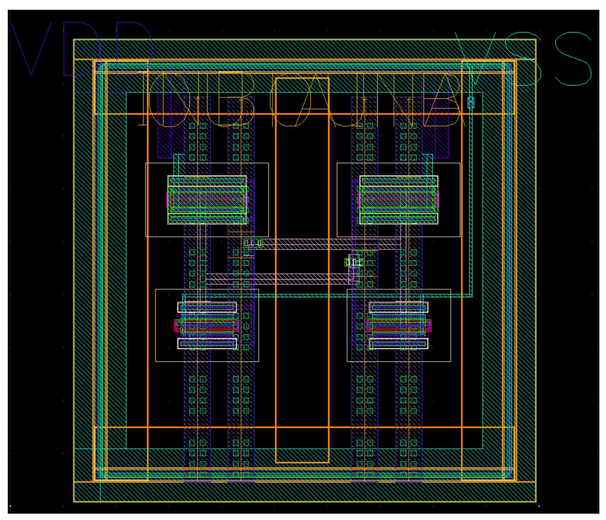
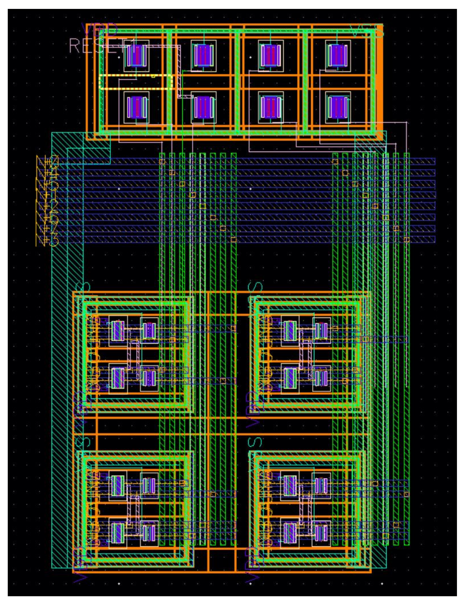
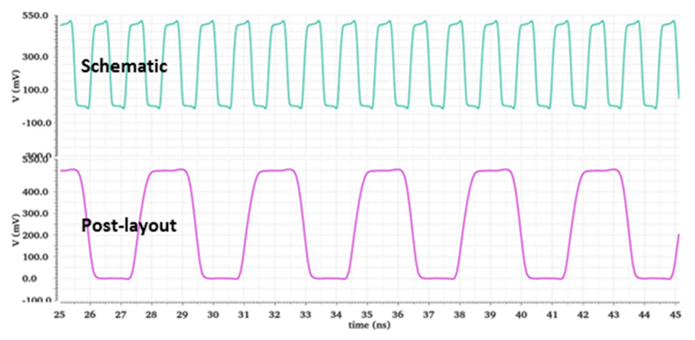
4.4. Layout Design and Post-Layout Simulation
5. Conclusions and State-of-the-Art Comparisons
Author Contributions
Funding
Data Availability Statement
Conflicts of Interest
References
- Hsieh, M.; Sobelman, G. Architectures for multi-gigabit wire-linked clock and data recovery. IEEE Circuits Syst. Mag. 2008, 8, 45–57. [Google Scholar] [CrossRef]
- Razavi, B. Challenges in the design high-speed clock and data recovery circuits. IEEE Commun. Mag. 2002, 40, 94–101. [Google Scholar] [CrossRef]
- Wei, Z.; Leduc, Y.; de Foucauld, E.; Jacquemod, G. Novel Building Blocks for PLL Using Complementary Logic in 28 nm UTBB-FDSOI Technology. In Proceedings of the IEEE NewCAS, Strasbourg, France, 25–28 June 2017; pp. 121–124. [Google Scholar] [CrossRef]
- Mao, Y. New Generation of Frequency Generators Using Self-Calibration of the Transistor Back Gate in FDSOI Technology. Ph.D. Thesis, Université Côte d’Azur, Nice, France, 2023. (In English). [Google Scholar]
- Wang, Y.; Zhang, L.; Han, W.; Li, X.; Lai, F.; Liu, X. A low-jitter PLL with new cross-coupled VCO delay cell for SerDes CDR in 55-nm CMOS technology. In Proceedings of the IEEE ICSICT, Hangzhou, China, 25–28 October 2016; pp. 1434–1436. [Google Scholar] [CrossRef]
- Liu, Y.; Wang, Y.; Jia, S.; Zhang, X. 180.5 Mbps-8 Gbps DLL-based clock and data recovery circuit with low jitter performance. In Proceedings of the IEEE ISCAS, Lisbon, Portugal, 24–27 May 2015; pp. 1394–1397. [Google Scholar] [CrossRef]
- Béraud-Sudreau, Q.; Begueret, J.-B.; Mazouffre, O.; Pignol, M.; Baguena, L.; Neveu, C.; Deval, Y.; Taris, T. SiGe Clock and Data Recovery System Based on Injection-Locked Oscillator for 100 Gbit/s Serial Data Link. IEEE J. Solid-State Circuits 2014, 49, 1895–1904. [Google Scholar] [CrossRef]
- Yan, D.L.; Raja, M.K.; Ajjikuttira, A.B. A Gated-Oscillator based Burst-Mode Clock and Data Recovery (CDR) Circuit. In Proceedings of the IEEE RFIT, Singapore, 9–11 December 2007; pp. 90–93. [Google Scholar] [CrossRef]
- Maruko, K.; Sugioka, T.; Hayashi, H.; Zhou, Z.; Tsukuda, Y.; Yagishita, Y.; Konishi, H.; Ogata, T.; Aoki, T.; Kihara, H.; et al. A 1.296-to-5.184 Gb/s Transceiver with 2.4 mW/(Gb/s) Burst-mode CDR using Dual-Edge Injection-Locked Oscillator. In Proceedings of the IEEE ISSCC, San Francisco, CA, USA, 7–11 February 2010; pp. 364–365. [Google Scholar] [CrossRef]
- Han, P.S.; Choi, W.Y. 10 Gbps injection-locked CDR with a simple bit transition detector in 0.18 μm CMOS technology. IEICE Electron. Express 2009, 6, 35–39. [Google Scholar] [CrossRef]
- Razavi, B. A study of injection locking and pulling in oscillators. IEEE J. Solid-State Circuits 2004, 39, 1415–1424. [Google Scholar] [CrossRef]
- Jacquemod, G.; Ben Abdeljelil, F.; Tatinian, W.; Lucchi, P.; Borgarino, M.; Carpineto, L. Comparison between RTW VCO and LC QVCO 12 GHz PLLs. Analog. Integr. Circuits Signal Process. 2012, 73, 749–756. [Google Scholar] [CrossRef]
- Wei, Z. Back-Gate Feedback for Auto-Calibration of Analog and Mixed Cells in UTBB-FDSOI Technology. Ph.D. Thesis, Université Côte d’Azur, Nice, France, 2019. (In English). [Google Scholar]
- Clerc, S.; Di Gilio, T.; Cathelin, A. The Fourth Terminal: Benefits of Body-Biasing Techniques for FDSOI Circuits and Systems; Springer: Cham, Switzerland, 2020. [Google Scholar] [CrossRef]
- Justo, D.; Cavalheiro, D.; Moll, F. Body bias generators for ultra low voltage circuits in FDSOI technology. In Proceedings of the DCIS, Barcelona, Spain, 22–24 November 2017; pp. 1–6. [Google Scholar] [CrossRef]
- Barajas, E.; Aragonés, X.; Mateo, D.; Moll, F.; Rubio, A.; Martín-Martínez, J.; Rodríguez, R.; Portí, M.; Nafría, M.; Castro-López, R.; et al. Analysis of Body Bias and RTN-Induced Frequency Shift of Low Voltage Ring Oscillators in FDSOI Technology. In Proceedings of the PATMOS, Platja d’Aro, Spain, 2–4 July 2018; pp. 82–87. [Google Scholar] [CrossRef]
- Arnaud, F.; Clerc, S.; Haendler, S.; Bingert, R.; Flatresse, P.; Huard, V.; Poiroux, T. Enhanced design performance thanks to adaptative body biasing technique in FDSOI technolologies. In Proceedings of the IEEE S3S, Burlingame, CA, USA, 16–19 October 2017; pp. 1–5. [Google Scholar] [CrossRef]
- Karel, A.; Comte, M.; Galliere, J.-M.; Azais, F.; Renovell, M. Impact of VT and Body-Biasing on Resistive Short Detection in 28 nm UTBB FDSOI—LVT and RVT Configurations. In Proceedings of the IEEE ISVLSI, Pittsburgh, PA, USA, 11–13 July 2016; pp. 164–169. [Google Scholar] [CrossRef]
- Guillaume, R.; Rivet, F.; Cathelin, A.; Deval, Y. Energy efficient distributed-oscillators at 134 and 202 GHz with phase-noise optimization through body-bias control in 28 nm CMOS FDSOI technology. In Proceedings of the IEEE RFIC, Honolulu, HI, USA, 4–6 June 2017; pp. 156–159. [Google Scholar] [CrossRef]
- Borjkhani, H.; Sheikhaei, S.; Borjkhani, M. Low Power Current Starved Sub-Harmonic Injection Locked Ring Oscillator. In Proceedings of the ICEE, Tehran, Iran, 20–22 May 2014; pp. 38–42. [Google Scholar] [CrossRef]
- Béraud-Sudreau, Q. Analysis and Design of an 80 Gbit/sec clock and Data Recovery Prototype. Ph.D. Dissertation, Université Sciences et Technologies—Bordeaux I, Talence, France, 2013. (In English). [Google Scholar]
- Dasdan, A.; Hom, I. Handling inverted temperature dependence in static timing analysis. ACM Trans. Des. Autom. Electron. Syst. 2006, 11, 306–324. [Google Scholar] [CrossRef]
- Samal, L.; Sahoo, S.R.; Samal, C. A Novel Temperature Invariant Ring Oscillator for Low Power Application. In Proceedings of the IEEE IICPE, Jaipur, India, 13–15 December 2018; pp. 1–5. [Google Scholar] [CrossRef]
- Jin, J.; Kim, J.; Kim, H.; Piao, C.; Choi, J.; Kang, D.S.; Chun, J.H. A 4.0-10.0-Gb/s Referenceless CDR with Wide-Range, Jitter-Tolerant, and Harmonic-Lock-Free Frequency Acquisition Technique. In Proceedings of the ESSCIRC, Dresden, Germany, 3–6 September 2018; pp. 146–149. [Google Scholar] [CrossRef]
- Choo, M.S.; Park, K.; Ko, H.G.; Cho, S.Y.; Lee, K.; Jeong, D.K. A 10-Gb/s, 0.03-mm2, 1.28-pJ/bit Half-Rate Injection-Locked CDR With Path Mismatch Tracking Loop in a 28-nm CMOS Technology. IEEE J. Solid-State Circuits 2019, 54, 2812–2822. [Google Scholar] [CrossRef]
- Wang, M.; Chen, Y.; Yuan, J. A low jitter 50 Gb/s PAM4 CDR of Receiver in 40 nm CMOS Technology. In Proceedings of the WCSP, Nanjing, China, 21–23 October 2020; pp. 349–352. [Google Scholar] [CrossRef]
- Lee, H.W.; Ko, K.M.; Kang, J.K. An 8–26 Gb/s Single Loop Reference-less CDR with Unrestricted Frequency Acquisition. In Proceedings of the ISOCC, Jeju Island, Republic of Korea, 6–9 October 2021; pp. 45–46. [Google Scholar] [CrossRef]
- Vert, D.; Pignol, M.; Lebre, V.; Moutaye, E.; Malou, F.; Begueret, J.B. A 3.2 GHz Injection-Locked Ring Oscillator-Based Phase-Locked-Loop for Clock Recovery. Electronics 2022, 11, 3590. [Google Scholar] [CrossRef]


| Process | VDD (V) | Temperature (°C) | Ouput Frequency (GHz) |
|---|---|---|---|
| TT | 0.5 | 27 | 0.868 |
| 0.5 | 125 | 1.45 | |
| 0.5 | −40 | 0.548 | |
| FF | 0.5 | 27 | 1.09 |
| 0.5 | 125 | 1.73 | |
| SS | 0.5 | 27 | 0.712 |
| 0.5 | −40 | 0.425 |
| VDD (V) | CK Jitter | PN (dBc/Hz@1 MHz) | Power Consumption (μW) | |
|---|---|---|---|---|
| Schematic | 0.5 | 0.6%UI | −122 | 235 |
| Post-layout | 0.63 | 2.3%UI | −118 | 318 |
| TT, 27 °C (Typical) | FF, 27 °C | FF, 125 °C (Fastest) | SS, 27 °C | SS, −40 °C (Slowest) | |
|---|---|---|---|---|---|
| Schematic | 868 MHz | 1.09 GHz | 1.73 GHz | 712 MHz | 425 MHz |
| Post-layout | 868 MHz | 1.03 GHz | 1.245 GHz | 757 MHz | 595 MHz |
| [24] | [25] | [26] | [27] | [28] | This Work | ||
|---|---|---|---|---|---|---|---|
| Technology (nm) | 28 | 28 | 40 | 28 | 180 | 28 | |
| Architecture | Half rate | Half rate | Half rate | Half rate | Full rate | Full rate | |
| CDR Type | PLL | Injection | PLL | PLL | Injection | Injection | |
| Supply Voltage (V) | 1.0 | 0.9 | 1.2 | 1.0 | 1.8 | 0.6 | 0.7 |
| Data rate (Gbps) | 10 | 10 | 50 | 20 | 3.2 | 0.868 | 2.4 |
| p-p Jitter (ps) | 8.8 | 26.8 | 1.6 | N/A | 6.4 mUI | 26.7 | 10.9 |
| Power Dissipation (mW) | 33 | 12.8 | 450 | 21.5 | 34.6 | 0.32 | 0.9 |
| Power efficiency (pJ/bit) | 3.3 | 1.28 | 9 | 1.08 | 10.81 | 0.37 | 0.37 |
| Core area (mm2) | 0.48 | 0.03 | N/A | N/A | 0.10 | 0.0012 (RO) 0.0066 (CDR) * | |
Disclaimer/Publisher’s Note: The statements, opinions and data contained in all publications are solely those of the individual author(s) and contributor(s) and not of MDPI and/or the editor(s). MDPI and/or the editor(s) disclaim responsibility for any injury to people or property resulting from any ideas, methods, instructions or products referred to in the content. |
© 2024 by the authors. Licensee MDPI, Basel, Switzerland. This article is an open access article distributed under the terms and conditions of the Creative Commons Attribution (CC BY) license (https://creativecommons.org/licenses/by/4.0/).
Share and Cite
Mao, Y.; Charlon, Y.; Leduc, Y.; Jacquemod, G. A Low Power Injection-Locked CDR Using 28 nm FDSOI Technology for Burst-Mode Applications. J. Low Power Electron. Appl. 2024, 14, 22. https://doi.org/10.3390/jlpea14020022
Mao Y, Charlon Y, Leduc Y, Jacquemod G. A Low Power Injection-Locked CDR Using 28 nm FDSOI Technology for Burst-Mode Applications. Journal of Low Power Electronics and Applications. 2024; 14(2):22. https://doi.org/10.3390/jlpea14020022
Chicago/Turabian StyleMao, Yuqing, Yoann Charlon, Yves Leduc, and Gilles Jacquemod. 2024. "A Low Power Injection-Locked CDR Using 28 nm FDSOI Technology for Burst-Mode Applications" Journal of Low Power Electronics and Applications 14, no. 2: 22. https://doi.org/10.3390/jlpea14020022
APA StyleMao, Y., Charlon, Y., Leduc, Y., & Jacquemod, G. (2024). A Low Power Injection-Locked CDR Using 28 nm FDSOI Technology for Burst-Mode Applications. Journal of Low Power Electronics and Applications, 14(2), 22. https://doi.org/10.3390/jlpea14020022