Abstract
An N-bit priority resolver having N inputs and N outputs functions as polling hardware in an embedded system, enabling access to a resource when multiple devices initiate access requests at its inputs which may be located on-chip or off-chip. Subsystems such as data buses, comparators, fixed- and floating-point arithmetic units, interconnection network routers, etc., utilize the priority resolver function. In the literature, there are many transistor-level designs for the priority resolver based on dynamic CMOS logic, some of which are modular and others are not. This article presents a novel gate-level modular design of priority resolvers that can accommodate any number of inputs and outputs. Based on our modular design architecture, small-size priority resolvers can be conveniently combined to form medium- or large-size priority resolvers along with extra logic. The proposed modular design approach helps to reduce the coding complexity compared to the conventional direct design approach and facilitates scalability. We discuss the gate-level implementation of 4-, 8-, 16-, 32-, 64-, and 128-bit priority resolvers based on the direct and modular approaches and provide a performance comparison between these based on the design metrics. According to the modular approach, different sizes of priority resolver modules were used to implement larger-size priority resolvers. For example, a 4-bit priority resolver module was used to implement 8-, 16-, 32-, 64-, and 128-bit priority resolvers in a modular fashion. We used a 28 nm CMOS standard digital cell library and Synopsys EDA tools to synthesize the priority resolvers. The estimated design metrics show that the modular approach tends to facilitate increasing reductions in delay and power-delay product (PDP) compared to the direct approach, especially as the size of the priority resolver increases. For example, a 32-bit modular priority resolver utilizing 16-bit priority resolver modules had a 39.4% reduced delay and a 23.1% reduced PDP compared to a directly implemented 32-bit priority resolver, and a 128-bit modular priority resolver utilizing 16-bit priority resolver modules had a 71.8% reduced delay and a 61.4% reduced PDP compared to a directly implemented 128-bit priority resolver.
Keywords:
priority resolver; embedded systems; digital circuits; logic design; ASIC; high-speed; low power; CMOS 1. Introduction
Subsystems such as data buses [1], comparators [2], fixed- and floating-point arithmetic units [3], interconnection network routers [4], incrementers/decrementers [5], and sequential address encoders of content addressable memory [6] typically rely on the priority resolver function. An N-bit priority resolver having N inputs and N outputs is commonly called an N-bit priority encoder [7,8] in the literature. Nevertheless, we shall use the term ‘priority resolver’ in this paper to refer to such a priority encoder and to distinguish it from a conventional priority encoder that has 2N inputs and N outputs. This is because no encoding is performed in an N-bit priority resolver. An N-bit priority resolver, when implemented in hardware, functions as a polling unit that enables access to a single resource when requests from multiple devices are received at its inputs, whether located on-chip or off-chip.
In the existing literature, several full-custom (i.e., transistor-level) designs for the priority resolver have been presented [5,8,9,10,11,12,13,14,15,16,17,18]. Many of these designs [5,8,9,10,11,12,13,14,15,18] are modular, meaning that small-size priority resolver modules are combined with any extra logic to form medium-/large-size priority resolvers, and some of the designs [16,17] are non-modular meaning they are not suitable for cascading and only serve as stand-alone priority resolvers. Some of the priority resolver designs [10,12] address a specific number of primary inputs (N = 64). A large majority of the priority encoder designs have been implemented in or make use of domino CMOS logic [5,9,10,11,12,13,14], while some priority encoder designs make use of dynamic CMOS logic [8,16,17,18]. Ref. [15] makes use of static CMOS logic and pass-transistor logic while Refs. [12,14] makes use of static CMOS and domino CMOS logic.
Most of the transistor-level designs of priority resolvers are based on the domino CMOS implementation style and correspond to active-high or active-low binary logic. Based on active-high logic, a priority resolver functions such that during the pre-charge phase of the clock, all the priority resolver outputs become binary 0. During the evaluation phase of the clock, the priority resolver output that corresponds to the input assuming the highest priority among the high inputs (i.e., set to binary 1) alone becomes binary 1, and the rest of the priority resolver outputs retain the value of binary 0. Based on active-low logic, a priority resolver functions such that during the pre-charge phase of the clock, all the priority resolver outputs become 1. During the evaluation phase of the clock, the priority resolver output that corresponds to the input assuming the highest priority among the low inputs (i.e., set to binary 0) alone becomes 0, and the rest of the priority resolver outputs retain the value of 1. Compared to active-high logic, which pre-charges all the priority resolver’s outputs to 0, in the case of active-low logic, all the priority resolver’s outputs are pre-charged to 1. This implies that the switching activity and the power dissipation tend to be higher for active-low logic compared to active-high logic [18]. Hence, active-high logic is preferable, and we used it for this work.
In a full-custom priority resolver design, the critical path is usually traversed through many NMOS or PMOS transistors depending upon its size. To reduce the (critical path) delay, transistor sizing may have to be performed. Transistor sizing may also have to be performed to ensure that the outputs of the priority resolvers can drive the required load(s). In general, compared to a full-custom (i.e., manual transistor-level) ASIC-style implementation, which requires substantial effort in terms of both design and characterization, a semi-custom (i.e., automated gate-level) ASIC-style implementation is preferable. This is because, in the case of a semi-custom design, a circuit/system can be described in a hardware description language (HDL) or a high-level language and then converted to HDL, which can be synthesized utilizing pre-characterized gates belonging to a standard cell library using a synthesis tool. Moreover, a semi-custom design method automates the synthesis for speed/area/power depending upon the optimization goal specified. On the contrary, the optimization for speed/area/power has to be performed manually in the case of a full-custom design, which might involve several design iterations. Further, a gate-level design of modular priority resolvers would be versatile, being suited for implementation in ASIC and FPGA design environments. Furthermore, an HDL description of a priority resolver could be made available as a soft intellectual property core that can be easily used off the shelf for integration into a sub-system or system design. Given these, in contrast to the existing work on priority resolvers which rely on a full-custom design approach, we focus on a semi-custom design approach in this paper. In this context, this article presents a novel gate-level modular priority resolver design strategy wherein small-size priority resolver modules can be combined with extra logic to efficiently realize medium- or large-size priority resolvers of any size.
In the rest of this article, Section 2 first describes the direct design approach for an N-bit priority resolver, and then the proposed modular design approach at the gate level. Section 3 discusses the physical realization of priority resolvers ranging from 4 bits up to 128 bits, implemented using both direct and modular design approaches, and gives their design metrics. Specifically, according to the proposed modular design approach, 4-bit priority resolver modules were used to implement 8-, 16-, 32-, 64-, and 128-bit priority resolvers; 8-bit priority resolver modules were used to implement 16-, 32-, 64-, and 128-bit priority resolvers; 16-bit priority resolver modules were used to implement 32-, 64-, and 128-bit priority resolvers; 32-bit priority resolver modules were used to implement 64- and 128-bit priority resolvers; and 64-bit priority resolver modules were used to implement 128-bit priority resolvers. Finally, Section 4 draws some conclusions from this research and highlights the potential scope for further work.
2. Priority Resolvers—Direct and Modular Design Approaches
In this section, we shall first discuss the direct design approach followed by the proposed modular design approach to realize N-bit priority resolvers.
2.1. Direct Design of Priority Resolvers
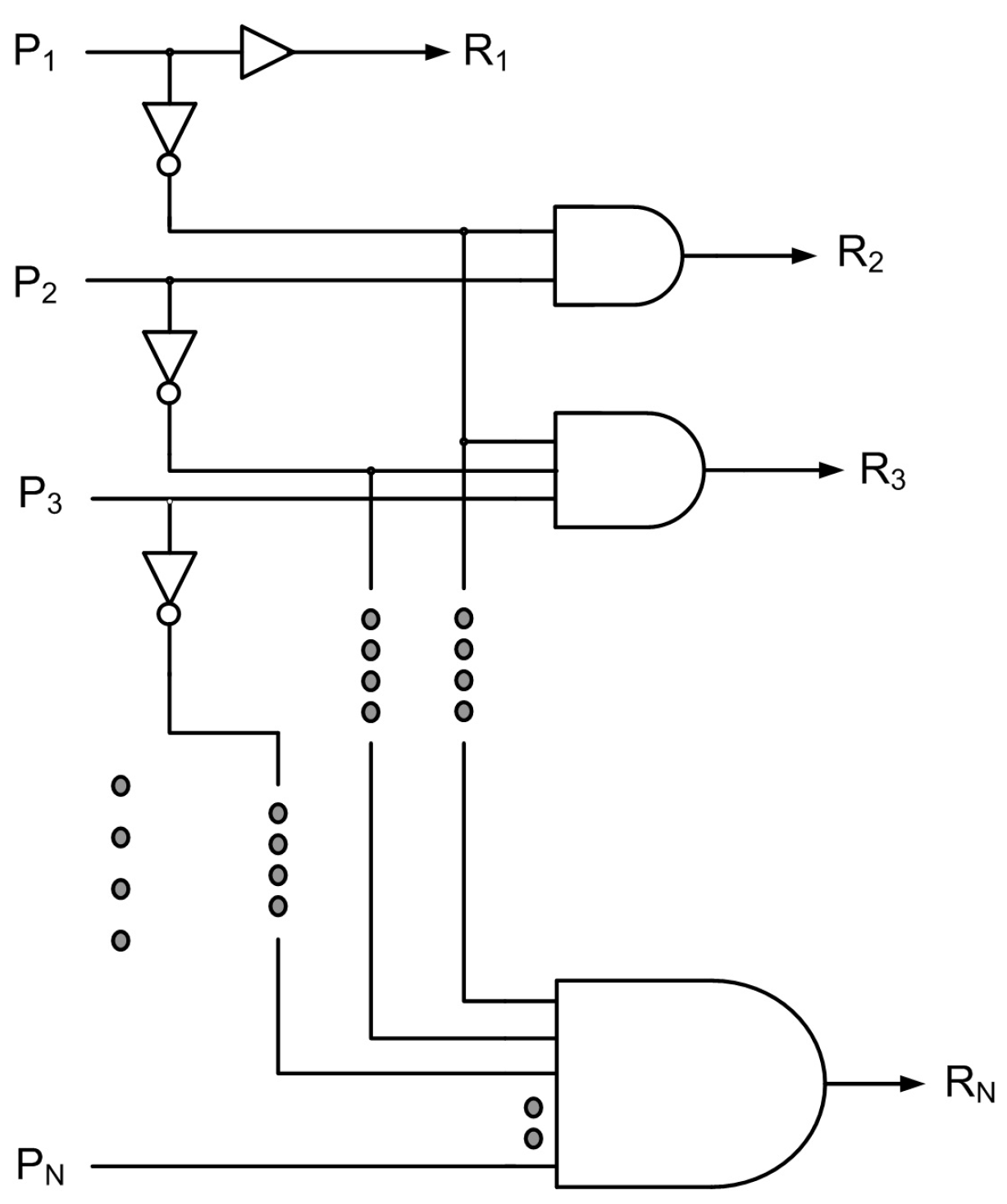
The direct implementation of an N-bit priority resolver having N inputs and N outputs is concisely shown in Figure 1, where P1 to PN represent the primary inputs and R1 to RN represent the primary outputs. Any primary input can be assigned the highest priority and any primary input can be assigned the lowest priority in a priority resolver. Accordingly, when the highest priority input is activated, the corresponding primary output would be activated to enable access for a device. In Figure 1, for example, primary input P1 is assigned the highest priority, and primary input PN is assigned the lowest priority with primary inputs P2 up to PN–1 assuming a descending order of priority down from P1. This implies that if P1 is activated (i.e., set to binary 1), R1 will be high (i.e., it will assume binary 1), and regardless of the rest of the primary inputs becoming activated or not during a processing time window, the remainder of the primary outputs will assume a value of 0. Supposing PN is activated, and if none of the other primary inputs are activated during a processing time window, the corresponding primary output RN will alone be high and the other primary outputs will assume a value of 0. Now assuming multiple primary inputs are activated, for example, if PN–3, PN–2, and PN–1 are activated during a processing time window, and the rest of the primary inputs P1 to PN–4 and PN remain deactivated during that time window, then RN–3 will alone be high. The rest of the primary outputs will assume a value of 0. This example scenario conveys that as the priority is passed down from the highest priority input down to lower priority inputs (when the highest priority input has not been activated), for the primary input that assumes the highest priority among the activated inputs, the corresponding primary output alone will be high. This principle is used to directly realize an N-bit priority resolver whose logic schematic is shown in Figure 1. In Figure 1, P1 and R1 are shown connected by a non-inverting buffer which is a standard for an ASIC-style implementation.

Figure 1.
Direct implementation of an N-bit priority resolver.
Assuming N to be 8 in Figure 1, an 8-bit priority resolver can be realized; its truth table is shown in Table 1. In Table 1, ‘d’ represents the do not care condition which may represent binary 0 or 1. Table 1 shows that if a primary input is set to 1, and provided that no higher-order primary input is concurrently set to 1, the primary output corresponding to that primary input will become 1 and the rest of the primary outputs will assume a value of 0. For example, if P1 = 1, regardless of the state of the other primary inputs P2 up to P8, R1 will assume a value of 1, and the rest of the primary outputs R2 up to R8 will assume a value of 0. To mention another example, if P4 = 1, and provided that P1 up to P3 have a value of 0, regardless of the state of P5 up to P8 (which signifies the do not care condition), R4 will assume a value of 1 while R1 up to R3, and R5 up to R8 will assume a value of 0. On the other hand, if P1 up to P8 have a value of 0, which is indicative of no activated inputs, R1 up to R8 would assume a value of 0.

Table 1.
Truth table of an 8-bit priority resolver. P1 up to P8 represent the primary inputs, and R1 up to R8 represent the primary outputs.
The outputs of the 8-bit priority resolver are expressed by Equations (1)–(8), where the symbol ~ signifies a Boolean complement. In Equations (1)–(8), the primary input P1 assumes the highest priority, and primary input P8 assumes the lowest priority with primary inputs P2 to P7 assuming a descending order of priority down from P1.
R1 = P1
R2 = P2 (~P1)
R3 = P3 (~P2) (~P1)
R4 = P4 (~P3) (~P2) (~P1)
R5 = P5 (~P4) (~P3) (~P2) (~P1)
R6 = P6 (~P5) (~P4) (~P3) (~P2) (~P1)
R7 = P7 (~P6) (~P5) (~P4) (~P3) (~P2) (~P1)
R8 = P8 (~P7) (~P6) (~P5) (~P4) (~P3) (~P2) (~P1)
A functional simulation of an 8-bit priority resolver was performed using Synopsys VCS by supplying all possible distinct input vectors, i.e., 256 input vectors for verification. The input vectors were supplied by a test bench at a latency of 2 ns. Figure 2 shows a screenshot of a portion of the simulation waveforms of the 8-bit priority resolver that was synthesized using a 28 nm CMOS standard digital cell library [19]. In Figure 2, bus p[7:0] encompassing inputs p[7] up to p[0] represents the primary input, and bus y[7:0] encompassing outputs y[7] up to y[0] represents the primary output.
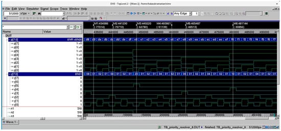
Figure 2.
Screenshot of a portion of simulation waveforms of an 8-bit priority resolver. Input bus p[7:0] comprises primary inputs p[7] up to p[0], with p[0] assuming the highest priority and p[7] assuming the lowest priority. Output bus y[7:0] comprises primary outputs y[7] up to y[0]. M1 to M6 are markers pointing to specific time instances in the simulation waveforms.
In the simulation waveform shown in Figure 2, six markers, namely M1 up to M6, are highlighted, which point to different combinations of primary inputs that are activated (i.e., set to 1) during different time instances and the corresponding highest-priority primary output that is high (i.e., become binary 1). The input and output states captured by the markers are mentioned below.
- Marker M1: primary inputs p[7], p[6], p[4], p[3], and p[0] are activated; primary output y[0] alone is high;
- Marker M2: primary inputs p[7], p[6], p[4], p[3], and p[2] are activated; primary output y[2] alone is high;
- Marker M3: primary inputs p[7], p[6], and p[5] are activated; primary output y[5] alone is high;
- Marker M4: primary inputs p[7], p[6], p[5], p[2], and p[1] are activated; primary output y[1] alone is high;
- Marker M5: primary inputs p[7], p[6], p[5], and p[3] are activated; primary output y[3] alone is high;
- Marker M6: primary inputs p[7], p[6], p[5], and p[4] are activated; primary output y[4] alone is high.
2.2. Proposed Modular Design of Priority Resolvers
A priority resolver of any size can be described in HDL according to the generalized logic schematic portrayed in Figure 1. However, it would be cumbersome to describe medium- and large-size conventional priority resolvers directly in HDL. In contrast, it would be rather convenient to describe a medium- or large-size modular priority resolver using small-size priority resolver modules and some additional logic, which is called a modular implementation. A modular implementation, besides simplifying the HDL coding, might help to minimize the critical path delay compared to a direct implementation. In this section, we present a novel gate-level modular priority resolver design architecture that can address any number of primary inputs and outputs and is suitable for a semi-custom ASIC-style implementation or an FPGA-based implementation.
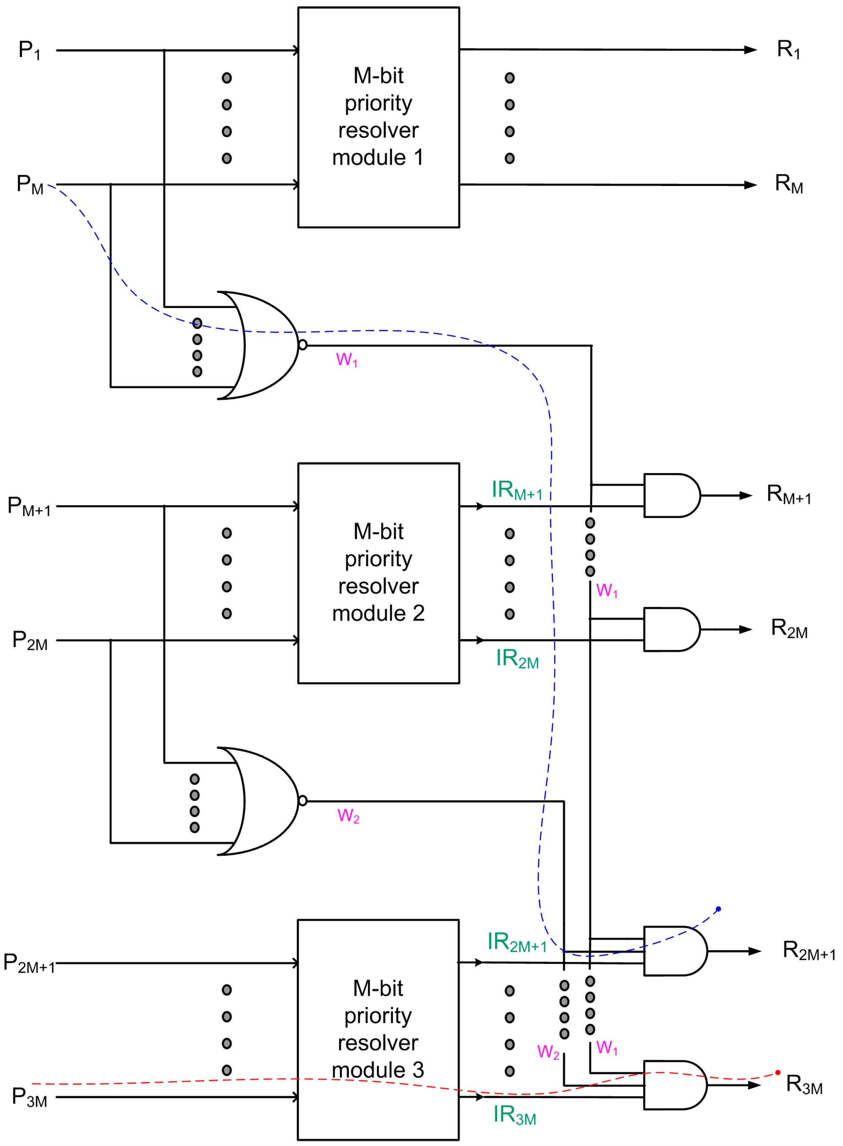
To describe our modular design approach, we now consider an M-bit priority resolver module and show how it can be used as a building block to realize an N-bit priority resolver where N > M, as depicted in Figure 3. For simplicity of discussion, in Figure 3, N and M are considered even, N is assumed to be equal to 3M, and N mod M is assumed to be 0. However, the proposed modular design architecture is generic and can be tailored to realize any N-bit priority resolver using the required number of M-bit priority resolver modules along with extra logic. Even if N mod M may not be equal to 0 and/or N is odd, a combination of different size priority resolver modules may be used to realize a modular N-bit priority resolver according to our proposition. In Figure 3, P and R represent the primary input and primary output, respectively.
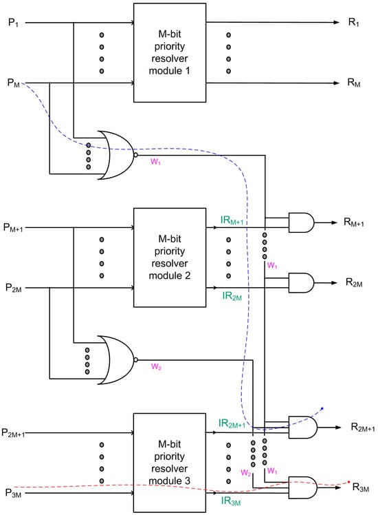
Figure 3.
Proposed modular design architecture to realize N-bit priority resolvers using M-bit priority resolver modules and extra logic. Here, N = 3M and N mod M = 0. The critical path may be traversed through an M-bit NOR gate and an (N/M)-input AND gate (which is highlighted by the blue dashed line) or an M-bit priority resolver module and an (N/M)-input AND gate (which is highlighted by the red dashed line). Internal outputs W1 and W2 are highlighted in pink, and the intermediate primary outputs IRM+1, IR2M, IR2M+1, and IR3M are highlighted in green.
Since N is assumed to be 3M for our discussion, three M-bit priority resolver modules are used, as shown in Figure 3, with module 1 having inputs P1 up to PM, module 2 having inputs PM+1 up to P2M, and module 3 having inputs P2M+1 up to P3M. In Figure 3, module 1 is assigned the highest priority while module 3 is assigned the lowest priority. In terms of the primary inputs, P1 is assigned the highest priority, and P3M is assigned the lowest priority in the modular N-bit priority resolver shown. W1 and W2 are internal outputs, which are the outputs of the M-bit NOR gates that comprise the inputs of module 2 and module 3, respectively. IRM+1 up to IR2M represents the outputs of priority resolver module 2, which are individually combined with W1 to produce the primary outputs RM+1 up to R2M. IR2M+1 up to IR3M represent the outputs of priority resolver module 3, which are individually combined with W1 and W2 to produce the primary outputs R2M+1 up to R3M.
Referring to Figure 3, to explain the modular design architecture, if any of the primary inputs of module 1 are activated, the output of the first M-bit NOR gate. viz. W1, would become 0. As a result, RM+1 up to R2M (representing the outputs of priority resolver module 2) and R2M+1 up to R3M (representing the outputs of priority resolver module 3) would become 0, regardless of whether any of their primary input(s) were activated. Supposing that none of the primary inputs of module 1 are activated, W1 would become 1, and the highest priority will now be passed to module 2. Under this condition, even if any one of the primary inputs of module 2 is activated, W2 would become 0, and hence, R2M+1 up to R3M (representing the outputs of priority resolver module 3) would become 0 regardless of whether any of its primary inputs were activated. If any module input is activated, the primary outputs belonging to modules with a lower priority would become 0 regardless of the active/inactive state of their corresponding primary inputs. This principle can be used to combine small-size priority resolver modules to realize medium- or large-size priority resolvers along with extra logic, as illustrated by the example realization shown in Figure 3.
3. Physical Implementation and Design Metrics
Priority resolvers of different sizes ranging from 4 bits to 128 bits were described in Verilog HDL according to the direct approach and the proposed modular approach and were synthesized using a 28 nm CMOS standard digital cell library [19]. For the modular design, different sizes of priority resolver modules were considered to implement larger-size priority resolvers. Specifically, 4-bit priority resolver modules were used to implement 8-, 16-, 32-, 64-, and 128-bit priority resolvers; 8-bit priority resolver modules were used to implement 16-, 32-, 64-, and 128-bit priority resolvers; 16-bit priority resolver modules were used to implement 32-, 64-, and 128-bit priority resolvers; 32-bit priority resolver modules were used to implement 64- and 128-bit priority resolvers; and 64-bit priority resolver modules were used to implement 128-bit priority resolvers along with extra logic.
A typical low-leakage standard cell library specification with a 1.05 V supply voltage and a 25 °C operating junction temperature was considered for the synthesis and simulation. Synopsys EDA tools, namely Design Compiler, was used for the synthesis and to estimate the total area (i.e., cells area + interconnect area) of the synthesized designs; VCS was used to perform the functional simulation; PrimeTime was used to estimate the (critical path) delay; and PrimePower was used to estimate the total (average) power dissipation. During the simulation and synthesis, the default wire load was used and a fanout-of-4 drive strength was assigned to all the priority resolver primary outputs. For the synthesis, the optimization goal was specified as speed. The critical path delay of the directly implemented 128-bit priority resolver was estimated to be 4.79 ns, and so the test benches corresponding to the various priority resolvers were supplied at a latency of 5 ns (@ 200 MHz) to simulate and verify their functionality. All the distinct input vectors were considered to simulate the functionality of the 4-bit and 8-bit priority resolvers. For 16-, 32-, 64-, and 128-bit priority resolvers, it would be cumbersome to consider all the distinct inputs since the number of distinct input vectors of an N-bit priority resolver is given by O[2N]. Hence, some random input vectors were considered to represent the test benches of 16-, 32-, 64-, and 128-bit priority resolvers. The same test benches were supplied to directly implemented and modular priority resolvers. The switching activity recorded during functional simulations was used to estimate the total power dissipation. A priority resolver usually forms a part of a sub-system that would be integrated into a system, and the clock is generally determined for an entire system. So, a virtual clock was used to constrain the input and output ports of the priority resolvers, and it did not form a part of the physical realization. Hence, the estimated design metrics of the various priority resolvers are entirely attributable to their corresponding logic.
The standard design metrics, viz. total area, critical path delay, and total power dissipation of directly implemented priority resolvers, are given in Table 2, and the same metrics corresponding to the modular priority resolvers are given in Table 3. In the first column of Table 3, the notation (X_Y) implies that an X-bit priority resolver module was used as the building block to construct a larger-size Y-bit priority resolver. Understandably, the 4-bit, 8-bit, 16-bit, 32-bit, and 64-bit priority resolvers that were realized directly were used as building blocks for the modular priority resolver designs.
Table 2.
Design parameters of directly implemented priority resolvers, synthesized using a 28 nm CMOS standard digital cell library.
Table 3.
Design parameters of (proposed) modular priority resolvers, synthesized using a 28 nm CMOS standard digital cell library.
From Table 2 and Table 3, it can be observed that the modular priority resolvers generally occupy more area compared to directly implemented priority resolvers. This is because, architecture-wise, modular priority resolvers, besides featuring the priority resolving logic, involve extra logic represented by the NOR and AND gates in Figure 3, which is absent in the directly implemented priority resolvers portrayed in Figure 1.
Although the area is a standard design metric, delay and power dissipation merit greater consideration than the area. From Table 2 and Table 3, it can be noted that for any given priority resolver size, the modular priority resolvers, regardless of the underlying priority resolver module used, had a reduced delay compared to the directly implemented priority resolvers. This may be reasoned theoretically as follows. The primary output of a directly implemented N-bit priority resolver that is assigned the least priority, i.e., RN in Figure 1, is produced by a final N-input AND gate. Supposing N = 128, a 128-input AND function is required to realize R128 according to the architecture shown in Figure 1. It is common knowledge that any large logic function would be decomposed by a logic synthesis tool before physical realization using a standard digital cell library. This is because modern standard digital cell libraries do not usually support AND gates with a fan-in > 4. Hence, even after logic decomposition, a 128-input AND function would give rise to multiple levels of logic in the critical path of a directly implemented 128-bit priority resolver. On the other hand, if we consider a 128-bit modular priority resolver implemented using say 16-bit priority resolver modules (referred to as a 16_128 modular priority resolver in Table 3), according to the architecture shown in Figure 3, the critical path may involve a 16-input NOR gate and an 8-input AND gate (as highlighted by the blue dashed line) or a 16-input AND gate and an 8-input AND gate (as highlighted by the red dashed line), and the high fan-in gates would be decomposed before physical synthesis. Nevertheless, either way, the critical data path of a 16_128 modular priority resolver would likely contain fewer logic gates compared to the critical path of a directly implemented 128-bit priority resolver, and this is the reason why modular priority resolvers, in general, have the potential to achieve reduced delay compared to directly implemented priority resolvers. This is substantiated by the delay metric given in Table 2 and Table 3. By comparing Table 2 and Table 3, the following observations were recorded.
- Compared to the directly implemented 8-bit priority resolver, a 4_8 modular priority resolver had a 29.3% reduced delay;
- Compared to the directly implemented 16-bit priority resolver, the 4_16 and 8_16 modular priority resolvers achieved reductions in delay of 31.5% and 38.4%, respectively;
- Compared to the directly implemented 32-bit priority resolver, the 4_32, 8_32, and 16_32 modular priority resolvers achieved similar reductions in delay of 40.2%, 41.7%, and 39.4%, respectively;
- Compared to the directly implemented 64-bit priority resolver, among the different modular priority resolvers, the 16_64 modular priority resolver achieved a maximum reduction in delay of 68.2%;
- Compared to the directly implemented 128-bit priority resolver, the 16_128 modular priority resolver achieved a maximum reduction in delay of 71.8%, and the 32_128 modular priority resolver achieved a similar delay reduction of 70.4%.
As noted earlier, the directly implemented priority resolvers occupied less area than the modular priority resolvers. Consequently, the former dissipates less power than the latter for all the priority resolver sizes considered. However, the product of power and delay, also called the power-delay product (PDP), commonly serves as a low power/low energy figure of merit for digital logic designs [20]. Therefore, we calculated the PDP of the directly implemented and modular priority resolvers for comparison, and these are given in Table 4.
Table 4.
Power-delay product (PDP) of direct and modular implementation of priority resolvers.
PDP is a useful figure of merit to quantify the energy efficiency of a digital logic design. From Table 4, it can be noted that from the PDP perspective, the modular implementation was preferable to the direct implementation for the different priority resolver sizes considered. This is mainly due to the significant delay reduction achieved by the modular implementation compared to the direct implementation. The following observations were made from Table 4:
- Compared to the directly implemented 8-bit priority resolver, a 4_8 modular 8-bit priority resolver had a 14% reduction in PDP;
- Compared to the directly implemented 16-bit priority resolver, the 4_16 and 8_16 modular 16-bit priority resolvers achieved reductions in PDP of 19% and 23%, respectively;
- Compared to the directly implemented 32-bit priority resolver, the 4_32, 8_32, and 16_32 modular 32-bit priority resolvers achieved similar reductions in PDP of 24.8%, 24.2%, and 23.1%, respectively;
- Compared to the directly implemented 64-bit priority resolver, among the different modular priority resolvers, the 16_64 modular 64-bit priority resolver achieved a maximum reduction in PDP of 56.8%;
- Compared to the directly implemented 128-bit priority resolver, among the different modular priority resolvers, the 16_128 and 32_128 modular 128-bit priority resolvers achieved similar reductions in PDP of 61.4% and 60.4%, respectively.
In general, choosing a small priority resolver module would result in the use of several such modules for a modular implementation. For example, a 4_128 modular priority resolver requires thirty-two 4-bit priority resolver modules which will increase the fan-in of the AND gates producing the primary outputs, as seen in Figure 3. This problem can be alleviated by using large priority resolver modules—for example, a 64_128 modular priority resolver requires just two 64-bit priority resolver modules and therefore, the fan-in of the final AND gates can be significantly reduced. However, a large priority resolver module would internally feature a large fan-in AND gate (evident from the logic corresponding to RN in Figure 1). Hence, the general idea is that to realize a medium- or large-size modular priority resolver, an optimally sized priority resolver module should be chosen such that the resulting modular implementation would comprise an optimum number of priority resolver modules to achieve the maximum reduction in delay and potentially the maximum reduction in PDP. For example, a 16_128 modular priority resolver was found to be optimal in Table 3 among the different 128-bit modular priority resolvers. The optimal size of a priority resolver module and the optimal number of priority resolver modules to be used to implement an optimum modular priority resolver may be determined by trial and error, as was performed in this work. Alternatively, a generalized mathematical model may be developed to guide the optimal implementation of a modular priority resolver.
From Table 2 and Table 3 concerning delay and power/PDP, we can infer that a 4_8 modular priority resolver is preferable to a directly implemented 8-bit priority resolver, 4_16 and 8_16 modular priority resolvers are preferable to a directly implemented 16-bit priority resolver, 4_32 and 16_32 modular priority resolvers are preferable to a directly implemented 32-bit priority resolver, a 16_64 modular priority resolver is preferable to a directly implemented 64-bit priority resolver, and a 16_128 modular priority resolver is preferable to a directly implemented 128-bit priority resolver.
4. Conclusions
Given that a priority resolver is a useful circuit in many embedded systems, this article presented a novel gate-level modular design strategy for the priority resolver. Compared to the existing transistor-level priority resolver designs which require considerable manual effort for both design and characterization, the proposed modular priority resolver design strategy corresponds to the gate level which makes it suitable for logic description using an HDL and subsequent synthesis using commercial/open-source EDA tools. Based on our proposition, an N-bit priority resolver can be implemented using M-bit priority resolver modules along with extra logic where N > M and N mod M may or may not be equal to 0. We considered different sizes of priority resolver modules for realizing many modular priority resolvers and compared their performance with directly implemented priority resolvers of the same size, based on a semi-custom ASIC-style implementation. It was noted that the proposed modular implementation of priority resolvers was preferable to the conventional direct implementation in terms of delay and PDP. As further work, the proposed modular priority resolver design strategy may be used to effectively realize incrementer/decrementer circuits and data comparators that utilize the priority resolver function. Also, the possibility of designing a 2D gate-level modular priority resolver may be explored as future work.
Author Contributions
Conceptualization, P.B.; methodology, P.B.; validation, P.B.; investigation, P.B. and D.L.M.; data curation, P.B.; writing—original draft preparation, P.B.; writing—review and editing, P.B.; visualization, P.B.; supervision, D.L.M.; project administration, P.B. and D.L.M.; funding acquisition, D.L.M. All authors have read and agreed to the published version of the manuscript.
Funding
This research was funded by the Singapore Ministry of Education (MOE) Academic Research Fund under grant number Tier-1 RG127/22.
Data Availability Statement
All data are available within the manuscript.
Conflicts of Interest
The authors declare no conflicts of interest. The funders had no role in the design of the study; in the collection, analyses, or interpretation of data; in the writing of the manuscript; or in the decision to publish the results.
References
- Adamides, E.D.; Iliades, P.; Argyrakis, I.; Tsalides, P.; Thanailakis, A. Cellular logic bus arbitration. IEE Proc. E Comput. Digit. Tech. 1993, 140, 289–296. [Google Scholar] [CrossRef]
- Huang, C.-H.; Wang, J.-S. High-performance and power-efficient CMOS comparators. IEEE J. Solid-State Circuits 2003, 38, 254–262. [Google Scholar] [CrossRef]
- Hennessy, J.L.; Patterson, D.A. Computer Architecture: A Quantitative Approach, 3rd ed.; Morgan Kaufmann Publishers: New York, NY, USA, 2002. [Google Scholar]
- Summerville, D.H.; Delgado-Frias, J.G.; Vassiliadis, S. A flexible bit-pattern associate router for interconnection networks. IEEE Trans. Parallel Distrib. Syst. 1996, 7, 477–485. [Google Scholar] [CrossRef]
- Huang, C.-H.; Wang, J.-S.; Huang, Y.-C. Design of high-performance CMOS priority encoders and incrementer/decrementers using multilevel lookahead and multilevel folding techniques. IEEE J. Solid-State Circuits 2002, 37, 63–76. [Google Scholar] [CrossRef]
- Mohan, N.; Fung, W.; Sachdev, M. Low-power priority encoder and multiple match detection circuit for ternary content addressable memory. In Proceedings of the IEEE International SOC Conference, Austin, TX, USA, 24–27 September 2006. [Google Scholar]
- Hashemian, R. A high speed compact priority encoder. In Proceedings of the 32nd Midwest Symposium on Circuits and Systems, Champaign, IL, USA, 14–16 August 1989. [Google Scholar]
- Delgado-Frias, J.G.; Nyathi, J. A VLSI high-performance encoder with priority lookahead. In Proceedings of the 8th Great Lakes Symposium on VLSI, Lafayette, LA, USA, 19–21 February 1998. [Google Scholar]
- Wang, J.-S.; Huang, C.-H. High-speed and low-power CMOS priority encoders. IEEE J. Solid-State Circuits 2000, 35, 1511–1514. [Google Scholar] [CrossRef]
- Kun, C.; Quan, S.; Mason, A. A power-optimized 64-bit priority encoder utilizing parallel priority look-ahead. In Proceedings of the IEEE International Symposium on Circuits and Systems, Vancouver, BC, Canada, 23–26 May 2004. [Google Scholar]
- Mohanraj, J.; Balasubramanian, P.; Prasad, K. Power, delay and area optimized 8-bit CMOS priority encoder for embedded applications. In Proceeding of the 10th International Conference on Embedded Systems and Applications, Las Vegas, NV, USA, 16–19 July 2012. [Google Scholar]
- Balobas, D.; Konofaos, N. Low-power, high-performance 64-bit CMOS priority encoder using static-dynamic parallel architecture. In Proceedings of the 5th International Conference on Modern Circuits and Systems, Thessaloniki, Greece, 12–14 May 2016. [Google Scholar]
- Balobas, D.; Konofaos, N. Ultra-low-power and compact 8-bit CMOS priority encoder. Int. J. Electron. Lett. 2017, 5, 272–278. [Google Scholar] [CrossRef]
- Balobas, D.; Konofaos, N. High-performance and energy-efficient 256-bit CMOS priority encoder. In Proceedings of the IEEE Computer Society Annual Symposium on VLSI, Bochum, Germany, 3–5 July 2017. [Google Scholar]
- Maurya, S.K.; Clark, L.T. Fast and scalable priority encoding using static CMOS. In Proceedings of the IEEE International Symposium on Circuits and Systems, Paris, France, 30 May–2 June 2010. [Google Scholar]
- Huang, S.-W.; Chang, Y.-J. A full parallel priority encoder design used in comparator. In Proceedings of the 53rd IEEE International Midwest Symposium on Circuits and Systems, Seattle, WA, USA, 1–4 August 2010. [Google Scholar]
- Panchal, P.; Vinitha, C.; Srivastava, R.; Balasubramanian, P.; Mastorakis, N.E. Design of 8-bit dynamic CMOS priority resolvers based on active-high and active-low logic. In Proceedings of the International Conference on Electronics and Communication Systems, Rhodes Island, Greece, 16–19 July 2013. [Google Scholar]
- Wang, X.; Feng, Y. Analysis and Design of 8-bit CMOS Priority Encoders. arXiv 2018, arXiv:1806.01443. [Google Scholar]
- Synopsys SAED_EDK32/28_CORE Databook, Revision 1.0.0. January 2012. Available online: https://www.synopsys.com/academic-research/university.html (accessed on 7 September 2023).
- Rabaey, J.M.; Chandrakasan, A.; Nikolic, B. Digital Integrated Circuits: A Design Perspective, 2nd ed.; Pearson Education: London, UK, 2003; ISBN 978-0130909961. [Google Scholar]
Disclaimer/Publisher’s Note: The statements, opinions and data contained in all publications are solely those of the individual author(s) and contributor(s) and not of MDPI and/or the editor(s). MDPI and/or the editor(s) disclaim responsibility for any injury to people or property resulting from any ideas, methods, instructions or products referred to in the content. |
© 2024 by the authors. Licensee MDPI, Basel, Switzerland. This article is an open access article distributed under the terms and conditions of the Creative Commons Attribution (CC BY) license (https://creativecommons.org/licenses/by/4.0/).