Article

Predicting the Performance of a 26 GHz Transconductance Modulated Downconversion Mixer as a Function of LO Drive and DC Bias

Department of Electronic & Electrical Engineering, The University of Sheffield, Sheffield S1 3JD, UK
Electronics 2022, 11(16), 2516; https://doi.org/10.3390/electronics11162516
Submission received: 6 July 2022 / Revised: 5 August 2022 / Accepted: 9 August 2022 / Published: 11 August 2022

Abstract

:
The dependency of RF performance on the local oscillator (LO) drive amplitude and DC bias is an important topic for RF mixers, especially as carrier frequency increases and generation of RF power thus becomes more complex. The prediction of mixer performance, without initial reliance on full circuit simulations, can provide important insights. In this work, mathematical models without the prior use of circuit simulation are developed, leading to a strategy to predict the conversion gain (Gc), DC current, 1 dB input compression point (IP1dB) and third order input intercept point (IIP3) for a SiGe bipolar transistor transconductance mixer. The models show the possibility to trade-off LO RF power and DC bias to achieve a desired performance. The concepts allow a prediction of the necessary DC bias required to support a chosen LO level and desired conversion transconductance or linearity. The mathematical model results, circuit simulation results, and measured hardware results from a 26 GHz prototype of a single-ended mixer are presented and compared, showing good agreement. In a lab-measured example, LO power reduction from +10 dBm to +3 dBm resulted in only a 1 dB reduction in conversion gain, by modifying the DC bias as predicted. The peak conversion gain predicted by the models is within 2.0 dB of circuit simulation and 2.5 dB of measured PCB results. The RMS error for predicted DC current, compared to circuit simulation, is 1.9 mA or better.

1. Introduction

The millimeter wave (mmWave) 5G bands at n258 (26 GHz) and n257 (28 GHz) are examples of the increasing adoption of mmWave frequencies for 5G and future 6G wireless communications [1]. A particular focus for mmWave systems is massive MIMO [2] which will require a multiplicity of low power RF hardware solutions at each antenna element. However, the operation of radios in the mmWave bands still requires power efficient and cost-effective RF circuit techniques to realize practical radio systems.
Whilst RF mixers can be designed and performance accurately predicted using CAD tools from the outset, this can lead to a loss of understanding of what affects the mixer performance. This is where mathematical models for circuit operation become valuable and allow fundamental insights into why particular effects or performance is seen.
Most mixer design strategies nowadays focus on FETs, due to their use in MMICs and CMOS designs. Such designs are well documented, with many published recent examples in CMOS at 28 GHz [3] and for 5G FR2 [4], 2.4 GHz [5], and increasingly at 60 GHz [6].
It is well known that the local oscillator (LO) drive power used for a frequency mixer can affect its gain, linearity and noise figure (NF). However, the generation of significant LO power at mmWave frequencies is today still complex, costly, and DC power inefficient. There is continued research interest in using simple, novel, and power-efficient RF architectures at mmWave, because of the generally higher DC bias currents and device costs as operational frequencies increase.

1.1. Paper Motivation

Development of mathematical models to allow the RF performance of a mmWave single-ended bipolar junction transistor (BJT) mixer design to be investigated, based on a known transistor, without the initial use of a circuit simulator. Existing published literature has focused extensively on FET mixers, with less recent attention on BJT mixers. This paper investigates the viability of trading LO RF power with DC bias in an SiGe NPN RF BJT transconductance modulated mixer, significantly expanding and improving the models and measurements developed in [7]. Mathematical models to predict the IF current generated by the mixing operation within the transistor are developed, leading to a prediction of the conversion transconductance (gmc) and conversion gain (Gc), 1 dB input compression point (IP1dB) and third order input intercept point (IIP3). The concepts are demonstrated using a commercial SiGe BJT.
Prediction of required DC bias for given LO power. A model is created for predicting the required DC base bias (Vb) to achieve a desired conversion transconductance with a chosen LO power, to allow the trading of RF performance in a predictable way. The concept can also be used to predictably control the conversion gain by adjusting Vb. Conventional mixer design approaches tend to set the DC bias and optimize the LO power for the best RF performance [8,9,10]. To the author’s best knowledge, the mathematical prediction of RF mixer performance by jointly selecting LO power and Vb has not been extensively explored previously, particularly relating to SiGe BJTs, although empirical relationship results have been observed and reported, for example [11].
Investigation into the use of low-cost commercial BJT in mmWave downconverting mixer. Although the focus of this paper is on the performance prediction of a single transistor downconversion mixer at 26 GHz, a hardware prototype was created using a commercial packaged transistor. This useful prototype has facilitated lab testing.

1.2. Background

Most recent literature for downconversion transistor-based mixer analysis and design are focused on CMOS, mainly using the Gilbert Cell architecture, (for example [12] at 24 GHz), though these can have poor performance at mmWave frequencies [13]. The related circuit analytical design often focuses on noise reduction techniques, with examples at 3.1 GHz [14] and 5G 27.5 GHz–43.5 GHz [15]. Linearity improvement techniques are also popular research topics for CMOS, such as for IIP3 in 802.15.4 at 2.4 GHz [16] or for second order input intercept point (IIP2) improvement [17]. Published works tend rely on subsequent circuit simulation for validation of trialed design techniques.
Single device (i.e., single-ended) downconverting mixers using GaAs transistors have been widely reported, for example [18] demonstrating a 6–26 GHz mixer requiring 13 dBm LO and [19] demonstrating a 5–30 GHz mixer requiring 15 dBm LO. However, SiGe devices can generally operate at lower bias current than GaAs and are readily available as discrete surface mount devices.
Only a few prior works fully develop and consider mixers with first-principles analysis techniques, such as for IIP2 and DC offset control [20], FET modelling [21], MOSFET modelling (100 MHz–1.5 GHz) [22]—generally all at carrier frequencies below 6 GHz. Where LO waveforms at the drain or collector are considered, standard models of clipped sinusoids are relied on, such as for 5G 24 GHz–40 GHz [23], leading to transconductance mixer models. For Gilbert Cell mixers, a hard switching waveform is assumed for commutation, such in WLAN 2.4 GHz [24]. However, the Gilbert Cell architecture is more complex than the mixer used in this paper, requiring three or more active devices.
Very few reported works compare the mathematical model results jointly to both circuit simulation and to a built prototype (3 steps), which makes it hard to assess the relative accuracies of approaches. They instead commonly focus on only comparisons between CAD simulation and lab measurements.
The mixer collector current is often modelled as a Taylor series in device transconductance, such as at 2.4 GHz [25], 1.7 GHz [26], 500 MHz–3.1 GHz [14] and this is the approach also taken in this paper for linearity analysis.
SiGe is an important semiconductor material for future mmWave communications systems due to its high performance and suitability for system integration [27,28,29]. Examples of its relevance to mixers are demonstrated in [30] for a 40 GHz mixer with 2 dBm LO drive. However, there are few recent works that consider BJT mixer design and analysis, even though this is relevant to SiGe BiCMOS at mmWave frequencies. This is because most mmWave designs have traditionally use GaAs PHEMTs or more recently CMOS (both using FET based models). Reported SiGe mixer designs are usually part of a larger integration, such as a front-end chip, with examples at 28 GHz for a phased array [31], IIP2 calibration techniques for 900 MHz WCDMA [32], 5G 26 GHz & 28 GHz receiver [33] and at 2 GHz [34]. However, the applicability of SiGe for higher mmWave operation is beginning to be reported in mixers, such as for 60 GHz ISM [35], a 0 dBm LO drive mixer at 60 GHz [36], and [37] presenting a 60 GHz Gilbert Cell with 3 dBm LO drive.
A design strategy for a single balanced BJT mixer in IC is provided in [38], though this uses 3 transistors. Also, like many Gilbert Cell designs, it also assumes the upper transistors act as switches with a 50% duty cycle. This is a simplification not used in this paper for the LO current model, with the whole waveform considered.
Reported results that compare modern CAD mixer circuit simulation to measured data at mmWave often show very good accuracies, often with circa 1 dB error for conversion gain, e.g.,: 77 GHz & 94 GHz mixer [39], 60 GHz [40], 5G 28 GHz [41], WIMAX [42], 5G 24 GHz–30 GHz [43], 26 GHz–40 GHz [44], though with up to 5 dB error for some designs [45]. Circa 3 dB simulator-referenced prediction errors for NF are reported, e.g., 77 GHz & 94 GHz [39], 5G 24 GHz–40 GHz [45] and 5G 28 GHz [41]. Fewer lab measurement to simulation comparisons of linearity have been published. However, [43] demonstrates IP1dB linearity measurements for a SiGe BiCMOS 5G 24 GHz–30 GHz mixer with LO operating at 20 GHz, which differs from simulations by circa 1dB.
A rare example that compares a calculated 950 MHz mixer conversion gain to measurements is reported in [46], showing a 1.5 dB overestimate from the calculation.
In general in the literature, mathematical models are used in the initial design process for selecting circuit values, with the CAD simulator then used to validate the design. The errors between models or simulations and measurements are often considered minor if circa 1 dB. However, the key requirements for a mixer (Gc, NF, IIP3) all have a great impact on the overall system performance. A difference of 1–3 dB can be significant for these parameters, hence the importance of model accuracy and a good understanding of the causes for performance, which theoretical models can provide.

1.3. Paper Contribution & Structure

The contributions of this paper are as follows: (1) new mathematical design models for predicting RF mixer IF and DC currents and hence Gc, considering both the base LO drive AL and DC base bias Vb without circuit simulation. (2) Models for predicting the IP1dB and IIP3 levels due to AL and Vb. (3) A model to guide the selection of base bias Vb, given a defined LO amplitude AL and desired conversion transconductance gmc. (4) Comparison and validation of the modelling approach to conventional circuit time-domain simulation and a measured hardware prototype single-ended 26 GHz mixer.
The paper is organized as follows: in Section 2, the models for the collector current are introduced and in Section 3, mathematical models for the IF current are developed. The hardware test prototype is introduced in Section 4. In Section 5, the mathematical models are compared to circuit simulation results and hardware lab trials. Section 6 concludes the paper.

2. Transistor Collector Current Mathematical Models

To facilitate a practical analysis, a commercial transistor was selected as the basis of the investigation and the resulting mixer design. The SiGe transistor BFP740FH6 from Infineon Ltd. was selected, with a transition frequency (FT) of 45 GHz. The first step in modeling the mixer operation is to create a representative collector current model. This requires an understanding of the device I-V characteristics at DC and at the center frequency of the LO. For the proposed mixer, an LO of 21 GHz was used. The conceptual representation of this initial test circuit for time-domain simulation is shown in Figure 1a. To allow a fully mathematical model to be created, a circuit model for the transistor’s basic operation was developed, as shown in Figure 1b, based on the Gummel Poon (GP) model [47].
The total collector current (combined AC and DC currents) caused by the base-emitter voltage, is represented by Io. Io can thus represent Ibm = Io(Vb) due to DC base bias Vb, or Ipk = Io(AL + Vb) due to the combined base AC LO signal and DC bias. The parameters of the GP model were obtained directly from vendor’s data sheets. All components shown in Figure 1b must be included to capture the AC and DC operation of the transistor.
The next step in building the mathematical model is to represent the relationship for Io at the LO as a function of an externally applied total voltage Vbe′, applied between the external base and emitter BJT pins. (Note: term Vbe is the total voltage seen between the internal base-emitter junction). Vbe can be related to Vbe′ using conventional circuit analysis techniques. Io is determined via mathematical circuit analysis and the GP BJT model, relating Vbe′ to Vbe and Io. The BJT internal collector current Ic is related to Vbe using Equation (1). In Equations (1)–(7), all terms are standard GP parameters, with values obtained from the BJT vendor’s data sheet model.
I c I s N q B ( e [ V b e N F × V T ] 1 )
The GP term NqB of Equation (2) is important for capturing the effects of current reduction due to DC bias and the LO AC drive.
N q B = q 1 s 2 ( 1 + 1 + 4 q 2 s )
The GP parameters q1s in Equation (3) represents the base-width modulation and q2s in Equation (4) represents high-level injection effects (including Kirk effect approximation).
q 1 s = 1 1 V b e V A R V b c V A F
q 2 s = I s I K F ( e [ V b e N F × V T ] 1 ) + I s I K R ( e [ V b c N R × V T ] 1 )
The GP internal capacitors Cbe of Equation (5) and Cbc of Equation (6) are also crucial in capturing the AC effects of the resulting collector current.
C b e = C J E ( 1 V b e V J E ) M J E + T F F × I s N F × V T × N q B e [ V b e N F × V T ]
C b c = C J C ( 1 V b c V J C ) M J C + T R × I s N R × V T × N q B e [ V b c N R × V T ]
The GP parameter TFF represents the transit time and is defined by Equation (7).
T F F = T F ( 1 + X T F [ I c I c + I T F ] 2 e [ V b c 1.44 V T F ] )
Parameters Cbc, Cbe, and NqB all have the effect of reducing the collector current achieved for a given Vbe for AC signals, leading to differing performance at AC and DC. The GP parameters used in the model for the BFP740F are listed in Table 1.
Figure 2 shows the equivalent AC comparison of the mathematical model compared to a Keysight ADS simulation as per Figure 1, showing a good fit over most of the range of interest for AL and Vb and so confirming the viability of the approach. This means the collector current due to LO can be accurately predicted and includes DC and AC effects, without CAD circuit simulation. It will be seen later that the LO waveform is vital to accurate mixer modelling. Figure 2 also shows the root mean square error (RMSE) between the ADS simulation and the model.
In general, let the applied external (base-emitter) voltage Vbe′ consists of three components: a base DC bias Vb, the LO signal of form A L cos ( ω L t ) and the incoming RF signal A R cos ( ω R t ) , combined for analysis as represented in Equation (8).
V b e = V b + A L cos ( ω L t ) + A R cos ( ω R t )

3. IF Current Mathematical Models

The prediction of the IF transconductance mixer current produced by the nonlinear action of the transistor is central to the calculations in this paper. This knowledge allows the proper and full consideration of base LO amplitude AL and base DC bias Vb on the creation of the IF current to be explored, supporting predictions of conversion transconductance gmc and IP1dB, etc. The mixer model uses the peak collector current Io(AL + Vb) and DC current Io(Vb) obtained using the device circuit mathematical model for the transistor described in Section 2. These current amplitudes are then applied to subsequent time-domain mathematical models representing the mixer action—this being more suitable for subsequent simple mathematical manipulation.

3.1. LO Currents

A conceptually valuable and well-known approach to modeling the operation of a transconductance mixer starts with the simple assumption that the collector current due to the LO produces a clipped sinusoidal waveform [48,49], as shown in Figure 3. Ipk is found using the model Equations (1)–(8) for Io(AL + Vb), providing the peak collector current due to the combined effect of base DC bias Vb and the AC LO signal AL, as applied to the external base-emitter. A simple time-domain sinusoidal current model, defined as i(t) = Ibm + (IpkIbm)cos(θ) is then used for subsequent mixer modeling, where θ is the phase of the LO in the cycle, Ipk is the peak collector current, and Ibm is the DC current due to Vb. Note that for all practical BJTs, there will be negligible current flowing in the period T1 to TpT1 because the collector will be off—hence the use of a clipped sinusoid model.
From Figure 3, parameter Tp is the period of the LO cycle and T1 is the time, as measured from the start of the waveform, where the collector current has fallen to a negligible value (i.e., transistor Vbe′ below knee). However, it has been found that as Vb is reduced and AL increased significantly, the collector current waveform is better modeled by ( I p k I b m ) cos(2θ). Between these states, transitional definitions are required, allowing the collector current time-domain model to better represent the actual transistor current waveform. The time-domain representation of this new fitting can be defined by Equations (9)–(11) which incorporates parameter k, which can vary from 1.0–2.0 thus representing ( I p k I b m ) cos().
I T k = I b m + ( I p k I b m ) cos ( 2 k π t T p ) ,   for   t = 0 T 1
I T k = I b m + ( I p k I b m ) cos ( 2 π [ 1 k ] + 2 k π t T p ) ,   for   t = T p T 1 T p
I T k = 0 ,   for   t = T 1 T p T 1
The Fourier coefficient for the resulting first harmonic C1 current is then represented by Equation (12) and Equation (13) for DC C0. Equation (12) defines C1k when k is not equal to 1; when k equals 1 Equation (14) should be used.
C 1 k = 2 I b m π sin ( 2 π T 1 T P ) + ( I p k I b m ) π { sin [ 2 π T 1 ( k + 1 ) T p ] k + 1 + sin [ 2 π T 1 ( k 1 ) T p ] k 1 }
C 0 k = 2 I b m T 1 T p + ( I p k I b m ) k π [ sin ( 2 k π T 1 T p ) ]
C 11 = 2 I b m π sin ( 2 π T 1 T P ) + 2 ( I p k I b m ) T 1 T p + ( I p k I b m ) 2 π [ sin ( 4 π T 1 T p ) ]
Parameter T1 can be defined by the simple geometry of the collector current waveform or the applied base voltage waveform Vbe′. Considering Equation (8) and ignoring the negligible contribution from AR, the point where Vbe′ intercepts BJT DC knee voltage Vtt (circa 0.75 V) can be used to define T1, using Equation (15). Although Vtt can be hard to predict in a real device, for the purposes of the simple model here it can be predicted as required from Equation (1).
T 1 = T p 2 π arccos ( V t t V b A L )
The equivalent steady-state DC current Ibm, the middle of the collector current amplitude cycle in Figure 3, is determined from Equation (1) by considering only Vb, without an AC AL signal applied. The value of k for a particular time T1 and Tp is determined using Equation (16), where m and f are linear parameters for a straight-line approximation, dependent only on Vb.
k = V b × m + f
The values for m and f are found via time domain comparison over one LO period, using BJT instantaneous current Io using Equations (1)–(8) when compared to Equations (9) and (10) over the Vb and AL ranges of interest. They do not require circuit simulation and only need evaluating once for a design. The BFP740F extracted values are m = −1.75 V−1 and f = 2.6.

3.2. Relating AL to Required Port LO Power

The mathematical models are driven by the LO amplitude AL and DC bias Vb, both applied directly at the base. In practice, the LO power will be applied to a port away from the transistor, passing through various LO/RF combining networks and RF matching, before reaching the base. An approximation of the actual LO power required at the port can be calculated using the following steps:
  • Select a target AL and Vb and let the mathematical model Equation (13) produce the resulting equivalent DC current draw C0k.
  • Use C0k and the BJT small-signal S parameters to estimate the base input reflection coefficient Γ i Equation (17), with Γ L set to −1, representing a collector short circuit to ground at the LO, as required for good mixer operation.
    Γ i ( C 0 k ) = S 11 + S 12 S 21 Γ L 1 S 22 Γ L
Then, convert from Γ i to the equivalent base input impedance Zi(C0k) and then to the equivalent base shunt input resistance Rp.
  • Use AL as applied to Rp to calculate the RF LO power LOP_b, as would be seen at the base.
  • Translate the power LOP_b back to the connector port, accounting for any expected intermediate RF stage insertion losses, due to combiners, etc.
The above approach has been used in this study and shows good agreement with Keysight ADS simulations for AL vs. applied port LO power.

3.3. Extracting the Transconductance Mixing Current

The C1k Fourier component Equation (12) can be converted to a transconductance at the LO using Equation (18). C1k and AL are both ‘large signals’, however they both properly capture the transistor operation in the large signal regime and so (18) is a valid approach for the time varying transconductance due to the LO in the BJT.
g m L O = C 1 k A L
The product of the LO modulated transconductance, Equation (18), and the RF signal entering the mixer at the carrier, A R cos ( ω R t ) , will result in an IF current, due to the conversion transconductance. This product of the RF input voltage and the time varying transconductance is fundamental to the mixer’s operation [48,50]. The conversion transconductance at one of the resulting sidebands can then be represented by Equation (19).
g m C _ m a x = g m L O 2
Note that g m C is a function of both AL and Ipk (itself a function of AL and Vb) and as such the transistor is not operating in a class-A linear bias due solely to Vb.
The resulting IF current is then the product of Equation (19) and the applied RF voltage AR. The resulting DC current C0k may result in the BJT’s effective input and output match changing from the initial design target (used to create the matching networks). Therefore, the BJT input and output match change, due to a change in the effective bias, must be considered when evaluating the resulting conversion gain. A simple strategy for this is to consider the effect of the impedance change at the base (RF) and collector (IF) and represent it as a reduction in effective conversion gain, with respect to the target design value, which would usually be a conjugate match. This effect is incorporated into the model using Equations (20)–(22).
g m c = g m c _ m a x × M B ( C 0 k ) × M C ( C 0 k )
M B ( C 0 k ) = R b ( C 0 k ) ( R b t a r g e t + R b ( C 0 k ) ) 2 + ( X b t a r g e t + X b ( C 0 k ) ) 2
M C ( C 0 k ) = R c t a r g e t ( R c t a r g e t + R c ( C 0 k ) ) 2 + ( X c t a r g e t + X c ( C 0 k ) ) 2
Parameter Rb is the real part of the base impedance, Xb is the imaginary part and with the target assumed to be the conjugate of the base impedance at the target design DC current. Similarly, parameter Rc is the real part of the collector impedance, Xc is the imaginary part, and the target is collector conjugate impedance at the DC operating target.

3.4. IP1dB & IIP3 Prediction Models

The IP1dB for the mixer can be predicted as a function of AL and Vb, using the LO currents for the fundamental (C1k) and third harmonic (C3k) and then relating them, as will now be introduced. A conventional approach is to define the IF current using derivatives of the conversion transconductance using a Taylor series [51,52], represented at the IF frequency by Equation (23). This model assumes there are no memory effects present.
I c I F = I C 0 + A r × g m 1 + A r 2 × g m 2 + A r 3 × g m 3 +
where, conversion transconductance g m 1 = d ( I c L O ) d ( V A L ) , g m 2 = d 2 ( I c L O ) d ( V A L ) 2 , g m 3 = d 3 ( I c L O ) d ( V A L ) 3 are evaluated from the collector current due to the LO. Once the conversion transconductances are known, the IP1dB Equation (24) and IIP3 Equation (25) can be obtained directly for the equivalent base RF voltages.
A R I P 1 d B = g m 1 g m 3 ( 10 [ 1 20 ] 1 )
A R I I P 3 = g m 1 g m 3 4 3
A technique will now be introduced that relates the magnitudes of the found Fourier LO harmonics C1k, C3k to the currents that would be produced by a simple Taylor exponential expansion and hence leading to the required gm1 and gm3. The technique starts by defining the IF collector current from only the LO, as passed through the simple BJT AC model Equation (26) and then expanding into a Taylor series using Equation (27).
I c L O = I D C × e A cos ( ω L O ) V T
I c L O = 1 + A cos ( ω L O ) + A 2 2 cos ( ω L O ) 2 + A 3 6 cos ( ω L O ) 3 +
Expanding Equation (27) and collecting terms produces Equation (28).
I c L O = ( 1 + A 2 4 ) + ( A + 3 A 3 24 ) cos ( ω L O ) + A 2 4 cos ( 2 ω L O ) + A 3 24 cos ( 3 ω L O )
Considering the fundamental LO term means we can immediately state that C1k = A and considering the third harmonic term C3k = A 3 24 . We can then find parameter A by evaluating the ratio of C3k/C1k, using Equation (29).
A = 24 C 3 k C 1 k
The magnitude of the third-harmonic collector current component C3k can be determined using Equation (30), based on the techniques from Section 3.1.
C 3 k = 2 I b m 3 π sin ( 6 π T 1 T P ) + ( I p k I b m ) π { sin [ 2 π T 1 ( k + 3 ) T p ] k + 3 + sin [ 2 π T 1 ( k 3 ) T p ] k 3 }
By considering the current generation action of Equation (28), we can now also directly state Equations (31) and (32) to relate the current components in terms of required transconductance.
g m 1 A L = A
g m 3 A L 3 = 3 A 2 24
As a penultimate step, the required ratio of gm1/gm3 can be found using Equations (29) and (33).
g m 1 g m 3 = 8 A L 2 A 2
The base-referred IP1dB equivalent voltage amplitude is then determined by Equation (24). The base RF voltage corresponding to the third order input intercept point can also now be predicted using Equation (25).

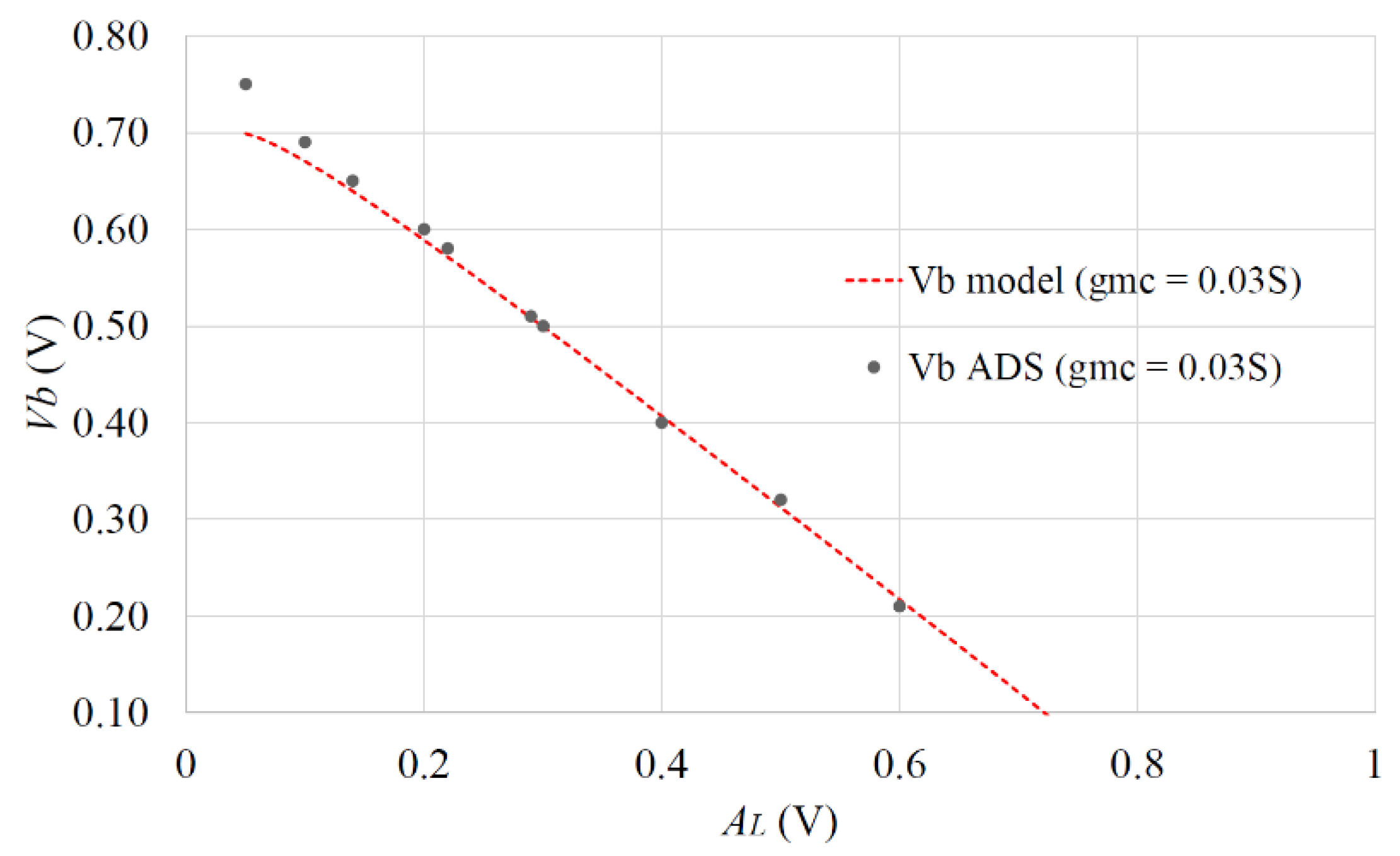
3.5. Selecting Vb for a Fixed AL and Conversion Transconductance

A key aim of the research was to identify the Vb required to support a particular desired conversion transconductance with a defined LO power. To lead to this, the expressions for k = 1 and k = 2 versions of Equation (12) using Equation (15) were derived. Applying the simplifying approximation of Ipk > Ibm and Vb < Vtt for practical mixers, allows usable simple expressions to emerge. However, in general we will not know early in a design whether to use k = 1 or k = 2 variants, so for a pragmatic approach an average is used. In addition, knowing that 0 < (Vtt-Vb) < AL allows a further simplification. We also know from Equations (18) and (19) that C1k = 2ALgmc. The above strategy leads to Equation (34) to define a simple relationship between Vb and a given AL and the desired gmc. (To further simplify Equation (34) NqB can reasonably be approximated to 1).
V b m = V T log e [ 2 π g m c × A L × N q B I s { 2 + [ π 4 + 11 12 ] e ( A L V T ) } ]
It may be tempting to rearrange Equation (34) to obtain gmc for a given Vb and AL but this should be avoided. (The applied simplifications would lead to an overestimate of gmc if used in this way. Accurate prediction of gmc requires full use of models as described in Section 3.1, Section 3.2 and Section 3.3).
Once proposed input and output matching circuits are known, the conversion gain can be predicted and thus converted to a trial gmc, following the architecture of Figure 4.

4. Trial Mixer Hardware for Model Validation

To evaluate the accuracy of the proposed IF current model (and subsequent conversion gain) required a BFP740F mixer prototype. The key requirement to ensure relevance to the mathematical model is that the mixer is base-driven for both the LO and RF signals and the IF current is extracted from the collector. A Keysight ADS circuit and planar EM simulation was created for the single-ended transistor mixer, as shown Figure 5, designed using conventional RF techniques.
The mixer LO range was 19–23 GHz and the RF range was 24–28 GHz. Rogers RO4003C substrate was used (0.5 mm thick, εr of 3.55, loss tangent of 0.0027). The input RF and LO signals are combined using a rat-race and then passed through a base conjugate matching network.
The output matching network is particularly important for transconductance mixers. Figure 6a shows the architecture used, with radial stub short circuits (S/C) at the collector port for the LO fundamental and its second harmonic, followed by an IF matching circuit and low pass filter (LPF). The collector network was biased at 3 V. To fully evaluate the mixer concepts, a 26 GHz PCB prototype was created from the developed ADS design. The assembled single-ended mixer PCB is presented in Figure 6b.

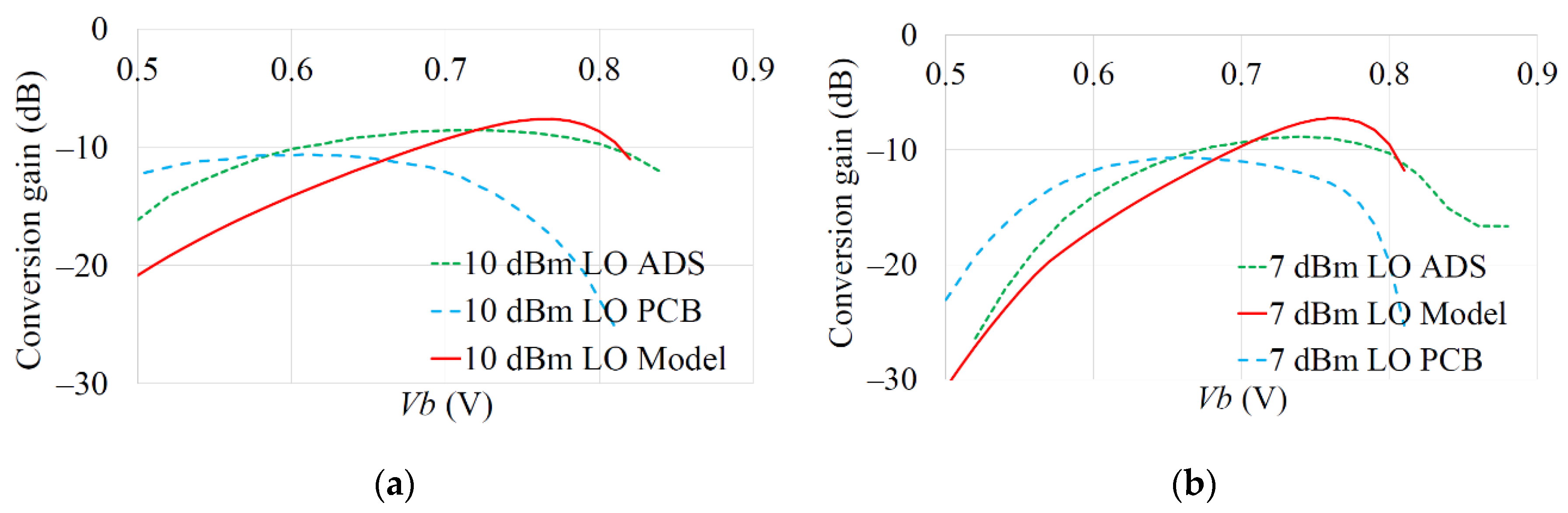
5. Comparison between Mathematical Models, Circuit Simulations and Measured PCB

The achievable RF performance and ALVb trade-offs were explored using the PCB protype mixer with 3 V collector bias. Unless stated, single frequency lab tests used a 21 GHz LO with port LO drive powers of 10, 7, 3 and 0 dBm. Unless stated, the RF signal was set to 26 GHz at −20 dBm, resulting in a 5 GHz IF. The RF signal generator was an Agilent E8247C and the LO signal generator was a Gigatronix 2540B. IF signals were measured using a Rohde & Schwarz FSV40N spectrum analyser.

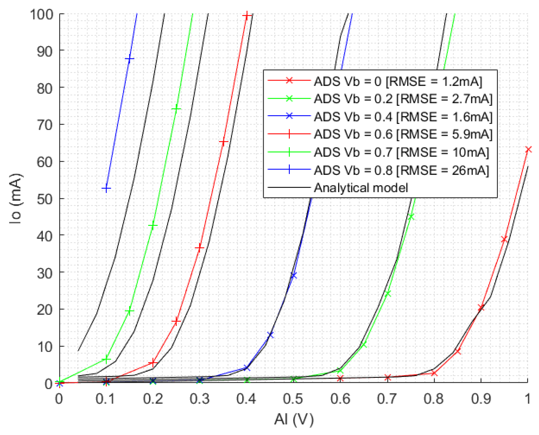
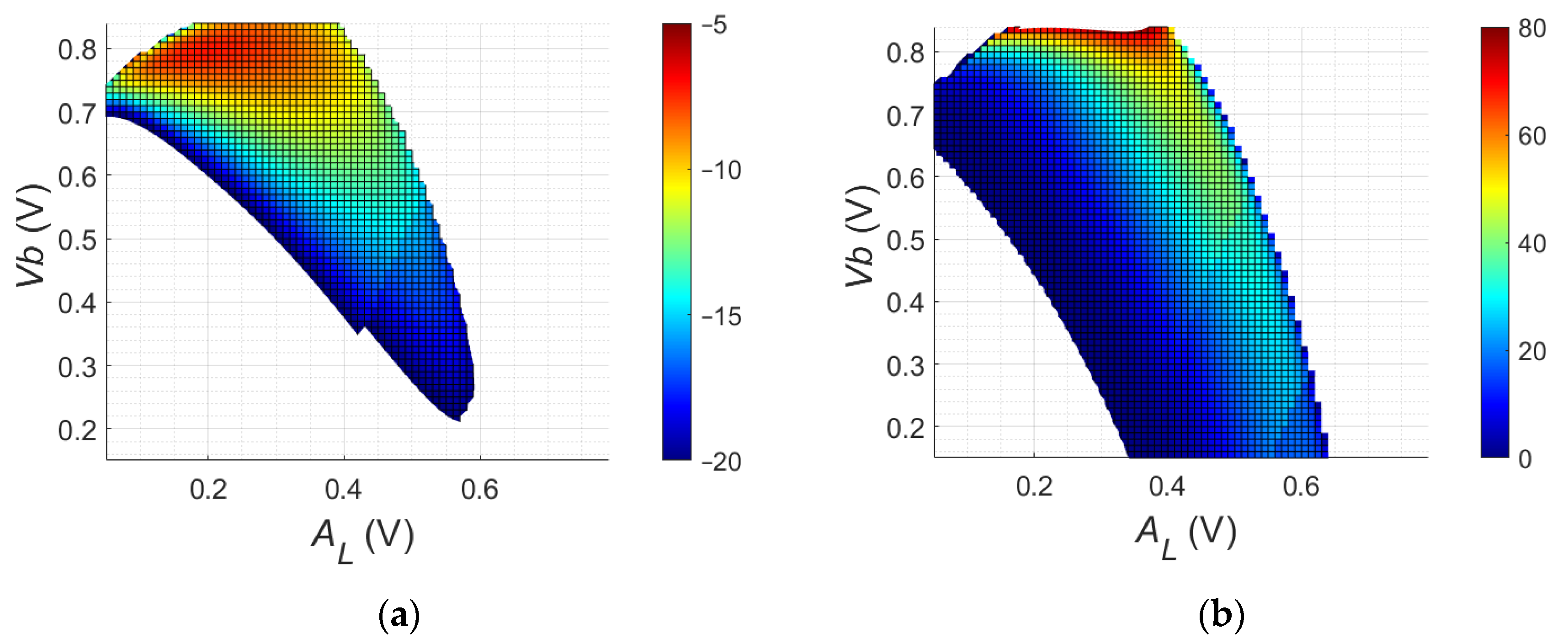
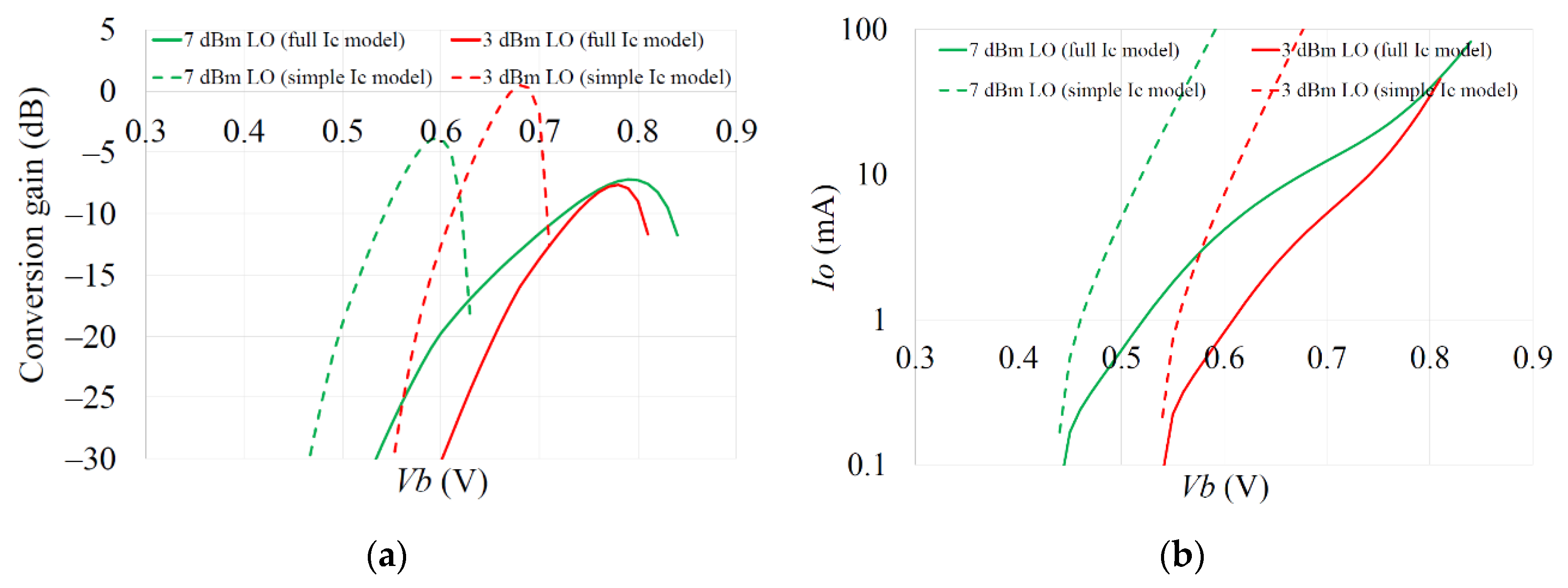
5.1. Initial Insights from Mathematical Model

The mathematical models based on Equations (1)–(22) were first used to explore the choice of Vb and AL on the produced IF current magnitude, resulting conversion gains and DC current draw. DC bias Vb was swept from 0 to 0.9 V and amplitude AL swept from 0 to 0.9 V, with RF input amplitude AR fixed. The resulting mixer IF conversion gains are shown in Figure 7a and the DC current draw in Figure 7b. A ridge for local optimum conversion gain can be seen in Figure 7a, starting at low Vb/high AL and showing a relationship between Vb and AL pairings for local optimum gain over the surface. There is also a clear upper peak gain area centered near Vb ~ Vtt. The region adjacent to the peak gain also shows further possible tradeoff between AL and Vb for a desired conversion gain near to peak.
The DC current consumption predicted by the mathematical model in Figure 7b highlights a rapid increase associated with increasing conversion gain towards maximum. Figure 7a shows that for a given fixed value of AL and simply adjusting Vb, a wide range of conversion gains can be achieved. It is proposed that in many systems it will be easier to vary Vb to control performance, whilst AL (LO power) will be fixed due to practical circuit implementation issues. By considering Figure 7a it can be seen that by adjusting Vb for a given AL, the gain can be peaked, confirming what has been reported experimentally by others [11]. By jointly considering Figure 7a,b allows operational points to be found for AL and Vb that give close to peak conversion gain but allow DC current to be minimized.
An example of predicting Vb for a given AL using model Equation (34), compared to the ADS circuit time-domain simulation, is presented in Figure 8. This shows good agreement between the model Equation (34) and the ADS circuit simulation, for achieving a 30 mS conversion transconductance.
Figure 9a shows the simulation using Equation (24) to calculate IP1dB is sensitive to both Vb and AL (LO power), with higher AL and higher Vb generally improving the achieved IP1dB, as might be expected. The input RF voltage corresponding to IIP3 can also now be predicted, using Equation (25), and is shown in Figure 9b, showing a similar trend. The P1dBI and IIP3 can also be seen to be more sensitive to Vb for lower LO powers.
The collector current full model consisting of Equations (1)–(7) and Figure 1b are necessarily complex to sufficiently represent the current. Figure 10a shows conversion gain and Figure 10b DC current at 7 dBm and 3 dBm LO powers, when comparing the results for the full collector current model and a simpler version just using Equation (1). The simple collector current model leads to a significant overestimate of collector current so cannot be used. Thus, comparisons using the full model are shown in Section 5.2.

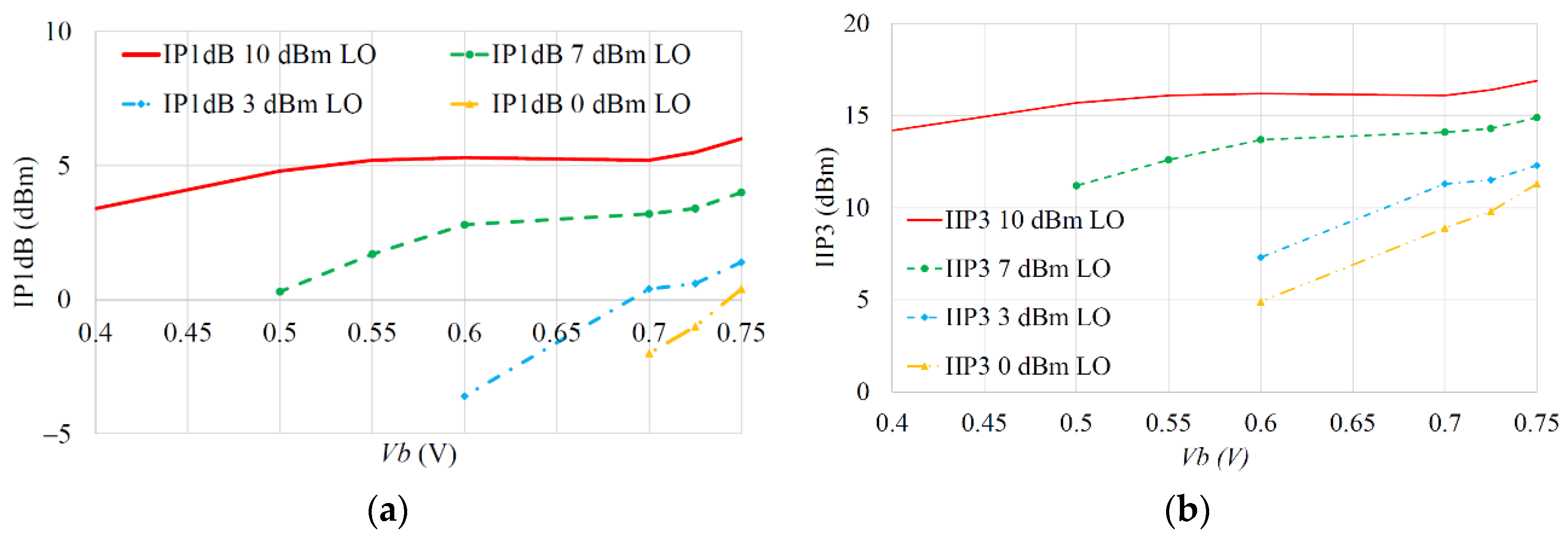
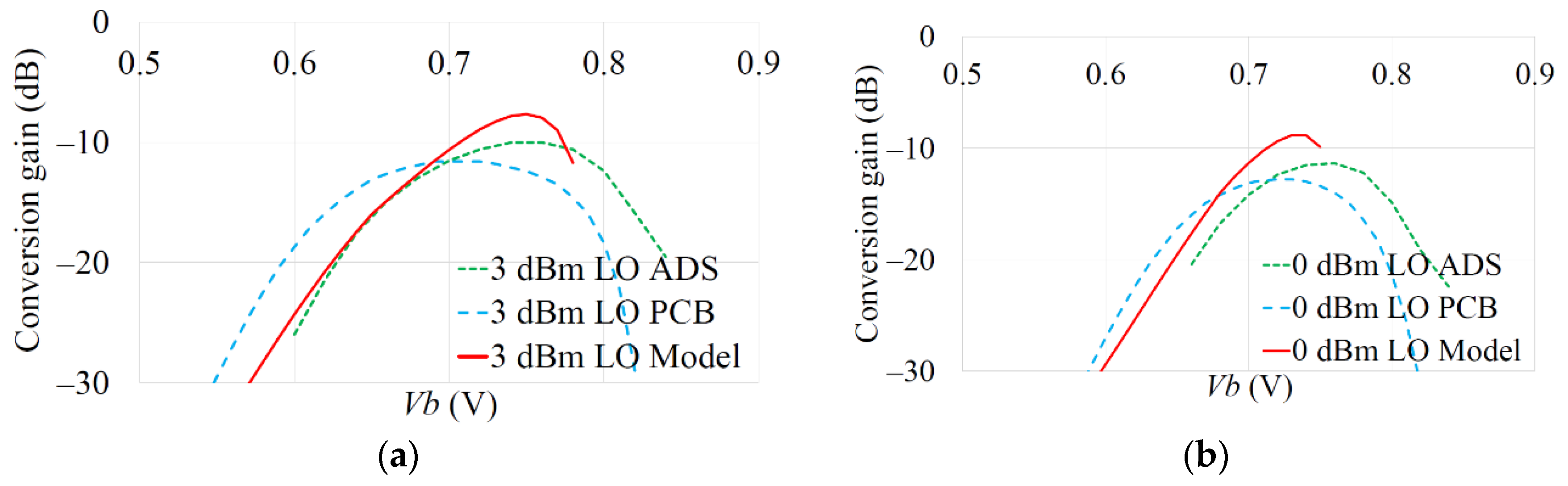
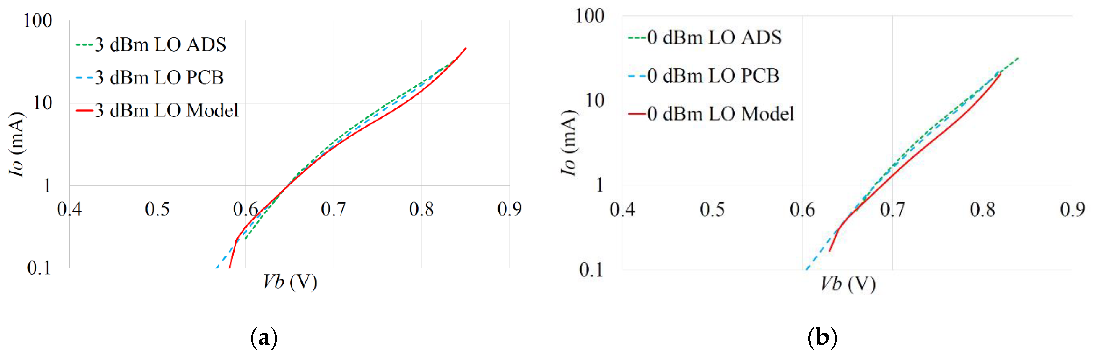
5.2. Lab Comparison Measurements of Hardware Mixer Prototype

The input rat-race combiner was tested within the implemented mixer, giving an LO to RF port isolation of 10 dB from 19 GHz to 25 GHz and 21 dB from 20 GHz to 23 GHz. The results of [7] show that simply defining a fixed consumed DC current and then adjusting Vb and AL to achieve the DC current will not result in constant gain. Thus, lab tests for this paper swept Vb for each LO drive level and measured the resulting conversion gain.
The resulting trade-off between the LO drive AL and bias Vb for a desired conversion gain can be observed in Figure 11 and Figure 12, comparing the mathematical model, Keysight ADS simulation and measured results. The DC current draw was also measured for the mixer configurations and is presented in Figure 13 and Figure 14. The various RMSE for the conversion gain and DC current are presented in Table 2. The errors in predicting the peak conversion gain are presented in Table 3. The DC currents show good agreement between the mathematical model, circuit simulations and measured PCB results, with RMSE errors better than 2 mA between the model and circuit simulations.
The general shape of the gain curves from the model, ADS simulation and PCB results show reasonable trend agreement. From Table 3, the model predicted peak Gc is within 2.0 dB of circuit simulation results and within 2.5 dB of measured PCB results. From Table 2, the RMSE of the model Gc compared to the measured PCB is similar to that due to full circuit simulation. The remaining error is possibly because, for simplicity, the model does not include all BJT current limiting aspects (which may require use of much more complex transistor models, such as Mextram and thus losing the convenience of the simple GP model). The FT of the BFP740F is 45 GHz (typical) so the relatively close operational frequency of the mixer and tolerancing of the real device may have also led to some of the differences seen compared to the measured data. An increased sensitivity to LO power on conversion gain, for operation close to FT, is seen in [53] for a Gilbert Cell architecture and this could also be an issue.
The published works discussed in Section 1.2 typically report a measurement to simulation error of circa 1 dB. However, there are very few published works that provide results of theoretical predictions of conversion gain or linearity as a function of base/gate DC bias and LO power. There are also very few works that have investigated the relationship between LO power and base/gate bias, which was a key motivator for this paper. In [8] the authors report conversion gain for an indium–phosphide (InP) double heterojunction BJT mixer with fixed bias operating in fundamental mode at 140 GHz, with an error in predicted Gc ranging from 0 dB to circa 10 dB over a range of LO powers. Table 2 shows a better prediction accuracy over a range of biases and powers (though at a lower carrier frequency). In [9] the authors show a InP High Electron Mobility Transistor acting as a mixer at 85 GHz and showing a decreasing conversion loss as LO power is increased, for two gate bias voltages. For high LO powers the conversion loss converges, as also seen in this work in Figure 11 and Figure 12. In [9] a 5 dB reduction in Gc is seen as the bias is reduced, a trend also predicted and seen in this paper. The authors of [10] present results for a GaAs (FET) mixer at 7.8 GHz, showing Gc measurements and theoretical predictions agreeing within circa 0.5 dB. This is notably better than the results in this work, but are at a lower frequency and with a FET technology rather than BJT. In [11] an E band SiGe BJT ring mixer is reported, with circuit simulation results showing that bias and LO amplitude can be traded (e.g., 0.3 V LO amplitude & 0.7 V bias give similar Gc to 0.7 V LO & 0.5 V bias)—as also proposed in this work and seen in Figure 11 and Figure 12. However, no theoretical calculation prediction of gain is provided. The authors of [11] report the measured conversion gain differs by circa 3 dB from that simulated. In [21] the gmc of a FET VHF mixer is seen to increase for increasing bias and increasing LO amplitude—as also seen here with the BJT.
By adjusting the base DC bias Vb, the single-ended mixer LO power was reduced from +10 dBm to +3 dBm, while suffering only a 1 dB drop in the conversion gain and benefitting from a 2 mA drop in DC draw. The accuracy of predicting Vb using Equation (34) was assessed, compared to the Vb required for the test PCB, in the lab for a desired gain and LO power. The error in predicting the required Vb over the range of LO powers was found to be less than 10%.
The measured PCB mixer conversion gain is negative largely owing to losses in the input combiner rat-race and network feeding the transistor base and choice of transistor. However, it should be noted that a negative conversion gain is common in simple single-device mixers operating at frequencies in the tens of gigahertz. Whilst it would be theoretically possible to de-embed the active part of the mixer so that it can be considered in isolation from passive circuits, it would still be necessary to include the effect of these losses when measuring and comparing to the test PCB. Therefore, the measurements reported here are compared to the RF ports of the built PCB and include the effect of all losses, allowing a direct comparison.
Figure 15 shows results from lab measurements of the mixer’s Gc across the RF input range 24 GHz–28 GHz with a 3 dBm LO and with various applied Vb (results are normalized to the Gc at 26 GHz). This shows the mixer’s measured conversion gain dependency on Vb is not a strong function of frequency—suggesting the single mathematical model can be used over the band.
A comparison of IP1dB for the prototype mixer and the model Equation (24) is presented in Figure 16a, showing good agreement between the mathematical model and laboratory measurements for all tested LO powers, with a model error of circa 1 dB. Figure 16b shows the comparison between the measured IIP3, an ADS harmonic balance (HB) simulation and Equation (25). Since the model underestimates the IP1dB, it could be expected to also underestimate the IIP3 by a similar amount. In practice, the model underestimates IIP3 by circa 5 dB. It is interesting to note that whereas the model tends to underestimate the IIP3 by 5 dB (or less) the ADS HB simulation tends to overestimate it by 5 dB. These results point to a general difficulty in modeling mixer nonlinearity, which can be sensitive to DC bias as also seen in [21], or possibly due to memory effects. However, the predicted IIP3 trend is correct and a ~5 dB uncertainty may be acceptable in early-stage designs. The authors of [20] show that IIP2 increases as LO power increases, to a certain point, as also seen in Figure 16b though for IIP3. This improvement in linearity for increasing LO power and sensitivity to Vb is also predicted in Figure 9a,b. Additionally [21] confirms the third order products reduce as LO drive increases, leading to an increased IIP3.
The RF input 3 dB bandwidth of the mixer was measured for an IF at 5 GHz and found to be 1.4 GHz (+10 dBm LO power). The IF 3 dB bandwidth of the mixer was also measured, and found to be 900 MHz, with an LO of 21 GHz and +10 dBm LO power.

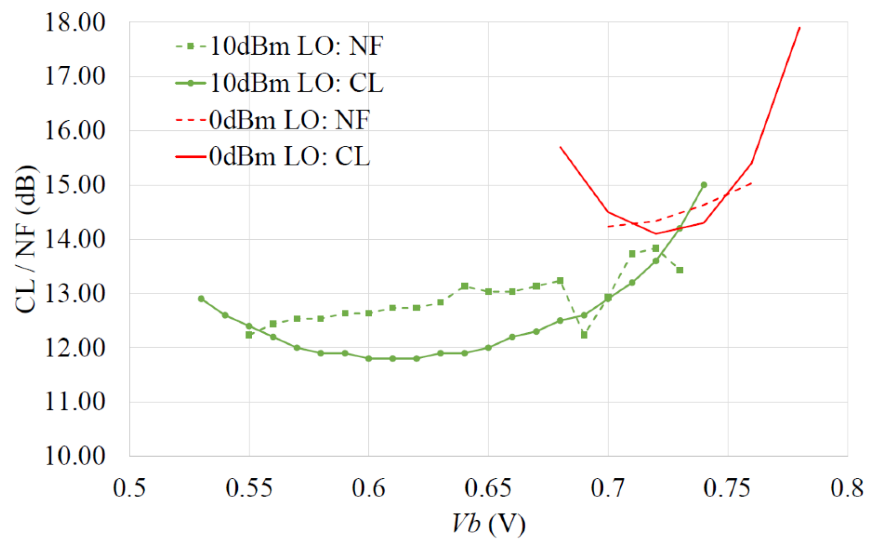
5.3. Noise Figure Measurements

Since the mixer has circa 10 dB conversion loss (CL), this will dominate any noise figure (NF) results. This was confirmed by measuring the single sideband (SSB) NF and associated conversion loss on the protype for 10 dBm and 0 dBm LO powers, as shown in Figure 17. The NF was measured using a noise diode (Keysight 346CK01) and spectrum analyzer with LNA (Keysight PXA N9030B) and evaluating the added noise from the mixer. The SSB NF of the mixer can be seen to be within 1 dB of the conversion loss, as expected. It is also worth noting from Figure 17 that if Vb is carefully selected (based on maximizing Gc), only a 2 dB degradation in NF will be suffered yet the LO power can be reduced by 10 dB.

6. Conclusions

It is shown that Gc, DC draw, IP1dB and IIP3 that can be achieved from a SiGe bipolar transistor downconverting mixer can be predicted to useful accuracy using the developed, simple mathematical models without recourse to full circuit simulation. Furthermore, an equation to predict the required Vb, for a base LO drive AL, to achieve a desired conversion transconductance is presented. The transconductance mixer mathematical models were compared to Keysight ADS circuit simulations and prototype hardware.
During tests, the mathematical model predicts peak conversion gain within 2.0 dB of circuit simulation results and within 2.5 dB of measured PCB results. The conversion gain RMSE between the model and circuit simulation is 3 dB worst-case, 1.3 dB best-case. The RMSE between predicted DC current and circuit simulation is below 2 mA. The model predicts IP1dB to 1 dB and IIP3 to circa 5 dB accuracies, with respect to the measured PCB.
Another key finding is that for operation below the peak Gc, the LO drive power can be traded for Vb bias while maintaining a defined conversion gain. An equally important finding is that conversion gain can be optimized by Vb as LO power is reduced and this can be predicted. This is an important finding because LO power is often challenging to generate at mmWave frequencies and impacts battery life of portable products. This also allows system designers using front-end mixers to configure them for a particular operational gain scenario, dynamically degrading gain and linearity where acceptable, to save power.
Although the model agrees well with simulation and measured results, some of the differences between the measured results and the mathematical models are likely due to the use of standard commercial uncharacterized surface-mount packaged transistors. The lab prototype used to validate the models also serves to demonstrate that a practical 26 GHz mixer can be realized using a low cost packaged transistor and conventional PCB design.
In general, mixer use-cases will likely have a primary design criterion based on NF/Gc or IIP3/P1dBi or obtaining best overall RF performance for a given available LO power. Hence, using the developed mathematical models, the following mixer scenarios can be investigated early in a design before embarking on a full circuit design:
  • NF/Gc: best settings for AL, Vb can be found and resulting IIP3/P1dBI predicted;
  • IIP3/P1dBI: best settings for AL, Vb can be found and resulting NF/Gc predicted;
  • Fixed LO power: Achievable NF, Gc, IIP3, P1dBi and DC power as function of Vb can be predicted;
  • Fixed DC power: Achievable NF, Gc, IIP3, P1dBi as function of LO power can be predicted.

Funding

This research was funded by UKRI, grant number MR/T043164/1. The APC was funded by the UKRI.

Conflicts of Interest

The author declares no conflict of interest.

References

  1. Hong, W.; Jiang, Z.H.; Yu, C.; Hou, D.; Wang, H.; Guo, C.; Hu, Y.; Kuai, L.; Yu, Y.; Jiang, Z.; et al. The Role of Millimeter-Wave Technologies in 5G/6G Wireless Communications. IEEE J. Microw. 2021, 1, 101–122. [Google Scholar] [CrossRef]
  2. Chataut, R.; Akl, R. Massive MIMO Systems for 5G and beyond Networks—Overview, Recent Trends, Challenges, and Future Research Direction. Sensors 2020, 20, 2753. [Google Scholar] [CrossRef] [PubMed]
  3. Yang, T.Y.; Chiou, H.K. A 28 GHz Sub-Harmonic Mixer Using LO Doubler in 0.18-Μm CMOS Technology. In Proceedings of the Digest of Papers—IEEE Radio Frequency Integrated Circuits Symposium, San Francisco, CA, USA, 10–13 June 2006; Volume 2006, pp. 209–212. [Google Scholar]
  4. Chang, Y.T.; Lin, K.Y. A 28-GHz Bidirectional Active Gilbert-Cell Mixer in 90-Nm CMOS. IEEE Microw. Wirel. Compon. Lett. 2021, 31, 473–476. [Google Scholar] [CrossRef]
  5. Kumar, S.; Saraiyan, S.; Dubey, S.K.; Pal, S.; Islam, A. A 2.4 GHz Double Balanced Downconversion Mixer with Improved Conversion Gain in 180-Nm Technology. Microsyst. Technol. 2020, 26, 1721–1731. [Google Scholar] [CrossRef]
  6. Varonen, M.; Kärkkäinen, M.; Kantanen, M.; Halonen, K.A.I. Millimeter-Wave Integrated Circuits in 65-Nm CMOS. IEEE J. Solid-State Circuits 2008, 43, 1991–2002. [Google Scholar] [CrossRef]
  7. Ball, E.A. Investigation into the Relationship Between Conversion Gain, Local Oscillator Drive Level and DC bias in a SiGe Transistor Transconductance Modulated Mixer at 24–28 GHz. In Proceedings of the IEEE Texas Symposium on Wireless & Microwave Circuits and Systems, Waco, TX, USA, 18 May 2021. [Google Scholar] [CrossRef]
  8. Yan, Y.; Bao, M.; Gunnarsson, S.E.; Zirath, H. A 110-170-GHz Multi-Mode Transconductance Mixer in 250-nm InP DHBT Technology. IEEE Trans. Microw. Theory Tech. 2015, 63, 2897–2904. [Google Scholar] [CrossRef]
  9. Ning, X.; Yao, H.; Wang, X.; Jin, Z. A W-Band Single-Ended Downconversion/Upconversion Gate Mixer in InP HEMT Technology. In Proceedings of the 2013 IEEE International Conference on Microwave Technology and Computational Electromagnetics, Qingdao, China, 25 August 2013. [Google Scholar] [CrossRef]
  10. Pucel, R.A.; Masse, D.; Bera, R. Performance of GaAs MESFET Mixers at X Band. IEEE Trans. Microw. Theory Tech. 1976, 24, 351–360. [Google Scholar] [CrossRef]
  11. Del Rio, D.; Gurutzeaga, I.; Rezola, A.; Sevillano, J.F.; Velez, I.; Gunnarsson, S.E.; Tamir, N.; Saavedra, C.E.; Gonzalez-Jimenez, J.L.; Siligaris, A.; et al. A Wideband and High-Linearity E-Band Transmitter Integrated in a 55-nm SiGe Technology for Backhaul Point-to-Point 10-Gb/s Links. IEEE Trans. Microw. Theory Tech. 2017, 65, 2990–3001. [Google Scholar] [CrossRef]
  12. Chen, J.D.; Wang, W.J. A K-Band Low-Noise and High-Gain Down-Conversion Active Mixer Using 0.18-Μm CMOS Technology. Wirel. Pers. Commun. 2019, 104, 407–421. [Google Scholar] [CrossRef]
  13. Beigizadeh, M.; Nabavi, A. Design of a High Gain and Highly Linear Common-Gate UWB Mixer in K-Band. Analog. Integr. Circuits Signal Process. 2014, 78, 501–509. [Google Scholar] [CrossRef]
  14. Solati, P.; Yavari, M. A Wideband High Linearity and Low-Noise CMOS Active Mixer Using the Derivative Superposition and Noise Cancellation Techniques. Circuits Syst. Signal Process. 2019, 38, 2910–2930. [Google Scholar] [CrossRef]
  15. Heidari, T.; Nabavi, A. Design and Analysis of a Wideband Compact LNA-Mixer in Millimeter Wave Frequency. Analog. Integr. Circuits Signal Process. 2020, 105, 371–383. [Google Scholar] [CrossRef]
  16. Gladson, S.C.; Bhaskar, M. A Low-Power RF Mixer with Harmonic Cancellation for IEEE 802.15.4 Portable, Wearable Wireless Applications. AEU-Int. J. Electron. Commun. 2020, 124, 153335. [Google Scholar] [CrossRef]
  17. Sivonen, P.; Vilander, A.; Pärssinen, A. Cancellation of Second-Order Intermodulation Distortion and Enhancement of IIP2 in Common-Source and Common-Emitter RF Transconductors. IEEE Trans. Circuits Syst. I Regul. Pap. 2005, 52, 305–317. [Google Scholar] [CrossRef]
  18. Nguyen, T.T.; Fujii, K.; Pham, A.-V. Highly Linear Distributed Mixer in 0.25-μm Enhancement-Mode GaAs pHEMT Technology. IEEE Microw. Wirel. Compon. Lett. 2017, 27, 1116–1118. [Google Scholar] [CrossRef]
  19. Nguyen, T.T.; Riddle, A.; Fujii, K.; Pham, A.-V. Development of Wideband and High IIP3 Millimeter-Wave Mixers. IEEE Trans. Microw. Theory Tech. 2017, 65, 3071–3079. [Google Scholar] [CrossRef]
  20. Kivekäs, K.; Pärssinen, A.; Halonen, K.A.I. Characterization of IIP2 and DC-Offsets in Transconductance Mixers. IEEE Trans. Circuits Syst. II Analog. Digit. Signal Process. 2001, 48, 1028–1038. [Google Scholar] [CrossRef]
  21. Surana, D.C.; Gardiner, J.G. Gain and Distortion Properties of FET Mixers and Modulators. IEEE Trans. Electromagn. Compat. 1974, EMC-16, 29–38. [Google Scholar] [CrossRef]
  22. Korotkov, A.S. Double-Balanced Mixer Based on MOSFETs. Russ. Microelectron. 2011, 40, 128–140. [Google Scholar] [CrossRef]
  23. Bae, B.; Han, J. 24-40 GHz Gain-Boosted Wideband CMOS Down-Conversion Mixer Employing Body-Effect Control for 5G NR Applications. IEEE Trans. Circuits Syst. II Express Briefs 2022, 69, 1034–1038. [Google Scholar] [CrossRef]
  24. Amirabadizadeh, S.; Bijari, A.; Alizadeh, H.; Mehrshad, N. Performance Improvement of a Down-Conversion Active Mixer Using Negative Admittance. Circuits Syst. Signal Process. 2021, 40, 22–49. [Google Scholar] [CrossRef]
  25. Bidi, A.A.S.; Karimi, G. Design of High Linearity Inductor-Less Active CMOS Mixer Based on Volterra Series Analysis. Circuits Syst. Signal Process. 2020, 39, 4810–4828. [Google Scholar] [CrossRef]
  26. García, J.A.; de La Fuente, M.L.; Zamanillo, J.M.; Mediavilla, A.; Tazón, A.; Pedro, J.C.; Carvalho, N.B. Intermodulation Distortion Analysis of FET Mixers under Multitone Excitation. In Proceedings of the 2000 30th European Microwave Conference, EuMC 2000, Paris, France, 2–5 October 2000; pp. 1–4. [Google Scholar]
  27. Xu, H.; Chen, J.; Wu, X.; Peng, C.; Yu, J.; Yuan, B.; Xie, Z. A 32–40 GHz 4-Channel Transceiver with 6-bit Amplitude and Phase Control. AEU Int. J. Electron. Commun. 2021, 139, 153925. [Google Scholar] [CrossRef]
  28. Avenier, G.; Diop, M.; Chevalier, P.; Troillard, G.; Loubet, N.; Bouvier, J.; Depoyan, L.; Derrier, N.; Buczko, M.; Leyris, C.; et al. 0.13 μ m SiGe BiCMOS Technology Fully Dedicated to Mm-Wave Applications. IEEE J. Solid-State Circuits 2009, 44, 2312–2321. [Google Scholar] [CrossRef]
  29. Wietstruck, M.; Marschmeyer, S.; Schulze, S.; Wipf, S.T.; Wipf, C.; Kaynak, M. Recent Developments on SiGe BiCMOS Technologies for Mm-Wave and THz Applications. In Proceedings of the 2019 IEEE MTT-S International Microwave Symposium (IMS), Boston, MA, USA, 2 June 2019; pp. 1126–1129. [Google Scholar]
  30. Pruvost, S.; Telliez, I.; Danneville, F.; Dambrine, G.; Rolland, N.; Pourchon, F. A 40 GHz Single-Ended Down-Conversion Mixer in 0.13 μm SiGeC BiCMOS HBT. IEEE Microw. Wirel. Compon. Lett. 2005, 15, 496–498. [Google Scholar] [CrossRef]
  31. Wang, X.; Guo, B.; Wu, J.; Gong, J. A 28 GHz Front-End for Phased Array Receivers Simulated in 180 Nm CMOS. In Proceedings of the 2020 IEEE International Conference on Semiconductor Electronics (ICSE), Kuala Lumpur, Malaysia, 28 July 2020; pp. 1–4. [Google Scholar]
  32. Kivekäs, K.; Pärssinen, A.; Ryynänen, J.; Jussila, J.; Halonen, K. Calibration Techniques of Active BiCMOS Mixers. IEEE J. Solid-State Circuits 2002, 37, 766–769. [Google Scholar] [CrossRef]
  33. Fonte, A.; Plutino, F.; Moquillon, L.; Razafimandimby, S.; Pruvost, S. 5G 26 GHz and 28 GHz Bands SiGe:C Receiver with Very High-Linearity and 56 DB Dynamic Range. In Proceedings of the 2018 13th European Microwave Integrated Circuits Conference (EuMIC), Madrid, Spain, 23 September 2018; pp. 57–60. [Google Scholar]
  34. Kivekas, K.; Parssinen, A.; Jussila, J.; Ryynanen, J.; Halonen, K. Design of Low-Voltage Active Mixer for Direct Conversion Receivers. In Proceedings of the ISCAS 2001—2001 IEEE International Symposium on Circuits and Systems, Conference Proceedings, Sydney, NSW, Australia, 6–9 May 2001; Volume 4, pp. 382–385. [Google Scholar]
  35. Reynolds, S.K. A 60-GHz Superheterodyne Downconversion Mixer in Silicon-Germanium Bipolar Technology. IEEE J. Solid-State Circuits 2004, 39, 2065–2068. [Google Scholar] [CrossRef]
  36. Mazor, N.; Sheinman, B.; Katz, O.; Levinger, R.; Bloch, E.; Carmon, R.; Ben-Yishay, R.; Elad, D. Highly Linear 60-GHz SiGe Downconversion/Upconversion Mixers. IEEE Microw. Wirel. Compon. Lett. 2017, 27, 401–403. [Google Scholar] [CrossRef]
  37. Qayyum, J.A.; Albrecht, J.D.; Ulusoy, A.C. A Compact V-Band Upconversion Mixer with -1.4-dBm OP1dB in SiGe HBT Technology. IEEE Microw. Wirel. Compon. Lett. 2019, 29, 276–278. [Google Scholar] [CrossRef]
  38. Sweet, A.A. Designing Bipolar Transistor Radio Frequency Integrated Circuits, 1st ed.; Artech House: Norwood, MA, USA, 2008; pp. 200–205. [Google Scholar]
  39. Reynolds, S.K.; Powell, J.D. 77 and 94-GHz Downconversion Mixers in SiGe BiCMOS. In Proceedings of the 2006 IEEE Asian Solid-State Circuits Conference, ASSCC 2006, Hangzhou, China, 13–15 November 2006; pp. 191–194. [Google Scholar]
  40. Choi, C.; Son, J.H.; Lee, O.; Nam, I. A +12dBm OIP3 60-GHz RF Downconversion Mixer with an Output-Matching, Noise- and Distortion-Canceling Active Balun for 5G Applications. IEEE Microw. Wirel. Compon. Lett. 2017, 27, 284–286. [Google Scholar] [CrossRef]
  41. Testa, P.V.; Szilagyi, L.; Xu, X.; Carta, C.; Ellinger, F. A Low-Power Low-Voltage Down-Conversion Mixer for 5G Applications at 28 GHz in 22-Nm FD-SOI CMOS Technology. In Proceedings of the Asia-Pacific Microwave Conference Proceedings, APMC, Hong Kong, 8–11 December 2020; pp. 911–913. [Google Scholar]
  42. Bhatt, D.; Mukherjee, J.; Redouté, J.M. Low-Power Switched Transconductance Mixer and LNA Design for Wi-Fi and WiMAX Applications in 65 Nm CMOS. IET Microw. Antennas Propag. 2018, 12, 1736–1744. [Google Scholar] [CrossRef]
  43. Yang, S.; Hu, K.; Fu, H.; Ma, K.; Lu, M. A 24-to-30 GHz Ultra-High-Linearity Down-Conversion Mixer for 5G Applications Using a New Linearization Method. Sensors 2022, 22, 3802. [Google Scholar] [CrossRef]
  44. Xu, L.; Wang, Z.; Li, Q. Design of a Broadband Millimeter-Wave Monolithic IQ Mixer. J. Infrared Millim. Terahertz Waves 2010, 31, 593–600. [Google Scholar] [CrossRef]
  45. Lee, D.; Lee, M.; Park, B.; Song, E.; Lee, K.; Lee, J.; Han, J.; Kwon, K. 24–40 GHz MmWave Down-Conversion Mixer with Broadband Capacitor-Tuned Coupled Resonators for 5G New Radio Cellular Applications. IEEE Access 2022, 10, 16782–16792. [Google Scholar] [CrossRef]
  46. Xavier, B.A.; Aitchison, C.S. Simulation and Modelling of a Heterojunction Bipolar Transistor Mixer. In Proceedings of the IEEE MTT-S International Microwave Symposium Digest, Albuquerque, NM, USA, 1–5 June 1992; Volume 1, pp. 333–336. [Google Scholar]
  47. Antognetti, P.; Massobrio, G. Semiconductor Device Modeling with SPICE, 2nd ed.; McGraw Hill: New York, NY, USA, 1993. [Google Scholar]
  48. Pozar, D.M. Microwave Engineering, 4th ed.; Wiley: Hoboken, NJ, USA, 2012; pp. 637–655. [Google Scholar]
  49. Maas, S.A. Nonlinear Microwave and RF Circuits, 2nd ed.; Artech House: Norwood, MA, USA, 2003; pp. 497–514. [Google Scholar]
  50. Robertson, I.D.; Lucyszyn, S. RFIC and MMIC Design and Technology, 1st ed.; The IET: London, UK, 2001; pp. 316–321. [Google Scholar]
  51. Kang, S.; Choi, B.; Kim, B. Linearity Analysis of CMOS for RF Applications. IEEE Trans. Microw. Theory Tech. 2003, 51, 972–977. [Google Scholar] [CrossRef]
  52. Liu, Z.; Dong, J.; Chen, Z.; Jiang, Z.; Liu, P.; Wu, Y.; Zhao, C.; Kang, K. A 62–90 GHz High Linearity and Low Noise CMOS Mixer Using Transformer-Coupling Cascode Topology. IEEE Access 2018, 6, 19338–19344. [Google Scholar] [CrossRef]
  53. Syu, J.S.; Meng, C.; Wang, C.L. 2.4-GHz Low-Noise Direct-Conversion Receiver with Deep N-Well Vertical-NPN BJT Operating near Cutoff Frequency. IEEE Trans. Microw. Theory Tech. 2011, 59, 3195–3205. [Google Scholar] [CrossRef]
Figure 1. BJT model used: (a) Initial simulation circuit to extract Io vs. Vb and AL; (b) Mathematical model for transistor operation, using Gummel Poon BJT parameters.
Electronics 11 02516 g001
Figure 2. Comparison of peak AC Io vs. AL for test ADS circuit simulation and GP mathematical model, showing good agreement.
Electronics 11 02516 g002
Figure 3. BJT collector LO current Io approximated by Ibm + Io(AL + Vb)cos(θ).
Electronics 11 02516 g003
Figure 4. Mixer signal locations.
Electronics 11 02516 g004
Figure 5. Single-ended 26 GHz mixer schematic.
Electronics 11 02516 g005
Figure 6. Single-ended 26 GHz mixer: (a) output network; (b) Built PCB (LO port on left and RF port on lower left, IF on right).
Electronics 11 02516 g006
Figure 7. Mathematical model: (a) conversion gain (dB); (b) DC current draw (mA).
Electronics 11 02516 g007
Figure 8. Comparison of Equation (34) vs. ADS simulation for Vb & AL to obtain 30 ms gmc.
Electronics 11 02516 g008
Figure 9. Linearity models as function of Vb and LO power: (a) IP1dB; (b) IIP3.
Electronics 11 02516 g009
Figure 10. Comparison of effect of simple and full model for collector current, as function of Vb and LO power on: (a) Conversion gain; (b) DC current.
Electronics 11 02516 g010
Figure 11. Model, ADS and measured PCB comparisons of mixer conversion gain as a function of Vb at: (a) 10 dBm LO drive; (b) 7 dBm LO drive.
Electronics 11 02516 g011
Figure 12. Model, ADS and measured PCB comparisons of mixer conversion gain as a function of Vb: (a) 3 dBm LO drive; (b) 0 dBm LO drive.
Electronics 11 02516 g012
Figure 13. Model, ADS and PCB comparison of mixer DC draw as a function of Vb and LO drive at: (a) 10 dBm; (b) 7 dBm.
Electronics 11 02516 g013
Figure 14. Model, ADS and PCB comparison of mixer DC draw as a function of Vb and LO drive at: (a) 3 dBm; (b) 0 dBm.
Electronics 11 02516 g014
Figure 15. Measured gain (normalized to gain at 26 GHz) across range 24–28 GHz as function of Vb (3 dBm LO drive).
Electronics 11 02516 g015
Figure 16. Measured and mathematical model comparison for IP1dB & IIP3 as function of LO drive level (Vb chosen to achieve peak gain for each tested LO drive power): (a) IP1dB; (b) IIP3.
Electronics 11 02516 g016
Figure 17. Measured mixer SSB NF and conversion loss (CL) for 10 dBm and 0 dBm LO drive.
Electronics 11 02516 g017
Table 1. Gummel Poon Model Parameters for BFP740F.
BJT Model ParameterValueUnitDescription
Is1.249 × 10−15ATransport saturation current
NF1.002-Forward current emission coefficient
NR1.01-Reverse current emission coefficient
VT25.9mVkT/q (25.9mV at 300K)
VAR1.229VReverse Early voltage
VAF380.1VForward Early voltage
IKF0.1898AForward Beta high current roll-off
IKR0.02753AReverse Beta high current roll-off
CJE0.2531pFBase-emitter zero-bias depletion cap
VJE0.9286VBase-emitter built-in potential
MJE0.06125-Base-emitter junction exponential factor
TF2.331pSIdeal forward transit time
XTF1.159-TF bias dependence coefficient
ITF0.3991ATF high current parameter
VTF0.5242VTF dependency on Vbc
CJC54.52fFBase-collector zero-bias depletion cap
VJC0.4808VBase-collector built-in potential
MJC0.5812-Base-collector junction exponential factor
TR1.532nSIdeal reverse transit time
RC4.1OhmInternal collector resistance
RE0.18OhmInternal emitter resistance
RB7.0OhmZero bias internal base resistance
RoVAF/IcOhmOutput resistance
BF987.1-Forward max Beta
Table 2. RMSE fitting error for conversion gain & DC current.
10 dBm LO7 dBm LO3 dBm LO0 dBm LO
Gc: Model-PCB8.06.04.32.7dB
Gc: ADS-PCB5.25.55.35.2dB
Gc: Model-ADS3.01.81.32.7dB
DC Draw: Model-PCB2.4-1.11.2mA
DC Draw: ADS-PCB3.4-0.70.6mA
DC Draw: Model-ADS1.61.61.91.7mA
Table 3. Error in peak conversion gain prediction.
10 dBm LO7 dBm LO3 dBm LO0 dBm LO
Gc: Model-PCB0.91.62.42.5dB
Gc: ADS-PCB3.03.53.94.0dB
Gc: Model-ADS2.01.81.61.4dB
Publisher’s Note: MDPI stays neutral with regard to jurisdictional claims in published maps and institutional affiliations.

