Article

Evaluation of Solder Joint Reliability in 3D Packaging Memory Devices under Thermal Shock

1
School of Microelectronics, Tianjin University, Tianjin 300072, China
2
China Electronic Product Reliability and Environmental Testing Research Institute, Guangzhou 510006, China
3
The State Key Laboratory of Precision Electronic Manufacturing Technology and Equipment, Guangdong University of Technology, Guangzhou 510006, China
4
Mechanical & Electrical Engineering College, Guangdong University of Technology, Guangzhou 510006, China
5
School of Information Engineering, Guangdong University of Technology, Guangzhou 510006, China
*
Authors to whom correspondence should be addressed.
These authors contributed equally to this work.
Electronics 2022, 11(16), 2556; https://doi.org/10.3390/electronics11162556
Submission received: 5 July 2022 / Revised: 10 August 2022 / Accepted: 11 August 2022 / Published: 16 August 2022

Abstract

:
In 3D packaging memory devices, solder joints are critical links between the chip and the printed circuit board (PCB). Under severe working conditions, cracks inevitably occur due to thermal shock. If cracks grow in the solder joint, the chip will be disconnected with the PCB, causing its function failure. In this paper, the reliability of solder joints under thermal shock are evaluated for 3D packaging memory devices by means of the SEM and finite element analysis. As microscopically studied by the SEM, it is found out that the main failure mechanism of solder joints in such test is the thermal fatigue failure of solder joints. Finite element analysis shows that cracks are caused by the accumulation of plastic work and creep strain. The initiation and growth of cracks are mainly influenced by the inelastic strain accumulation. The trends of cracks are influenced by the difference between the coefficient of thermal expansion (CTE) of epoxy resin and that of the chip.

1. Introduction

In the past decades, the equipment has higher and higher requirements for high-performance integrated circuit devices [1]. How to build a more functional chip system in a smaller space has become a challenging problem in the field of electronics. With the development of the integration technology of logic circuits and chips [2,3], 3D packaging memory device has become a promising choice of memory devices in more and more electronic industries [4,5], having the advantages of integration of many different functions and compact structures [6,7].
When the circuit is functioning, the 3D packaging memory device in the circuit will be subjected to various loads, such as mechanical stress and thermal stress [8]. Statistically, thermal fatigue failure and mechanical fatigue failure account for about 55% and 20% in its failures, respectively [9,10]. In order to ensure that the high-performance electronic device has a longer service life in extreme environments, many researchers have conducted extensive researches via various failure analysis models, such as thermal cycle model (low cycle fatigue, N f < 104) [11,12]. Compared with the 2D packaging device, the 3D packaging device has the advanges of smaller sizes, lower power consumption, and larger bandwidth [13]. However, it has serious problems with heat radiation since several chips are stacked in its small package, which will influece its long-term reliability [14]. Specically, the 3D packaging memory device adopts epoxy resin for filling to protect the device, which can excellently avoid the damage of vibration to the device [15]. However, the coefficient of thermal expansion (CTE) mismatch between the epoxy resin and various interfaces of the chip will lead to delamination or fracture between the epoxy resin layer and the substrate [16], which will further result in internal connection failure and the failure of the device. When the temperature exceeds 0.5 times of the melting point of the metal material, the metal material will be subjected to continuous stress, which will result in its slow plastic deformation. This phenomenon is called metal creep [17]. When the solder joint material creeps, plastic stress and strain will appear in the solder joint material, resulting in cracks and cavities in the solder joint [18].
Many researchers have employed the scanning electron microscope (SEM) and finite element analysis to study the interface fracture and fatigue cracking behavior of solder joints of chips [19,20,21]. Their results show that the chip has delamination failure behavior and solder joint creep under thermal shock. In this paper, we study the failure behavior of 3D packaging memory devices under thermal shock and evaluate their thermal reliability by means of experimental analysis and finite element analysis. Additionally, the relevant failure mechanism under thermal shock is discussed.

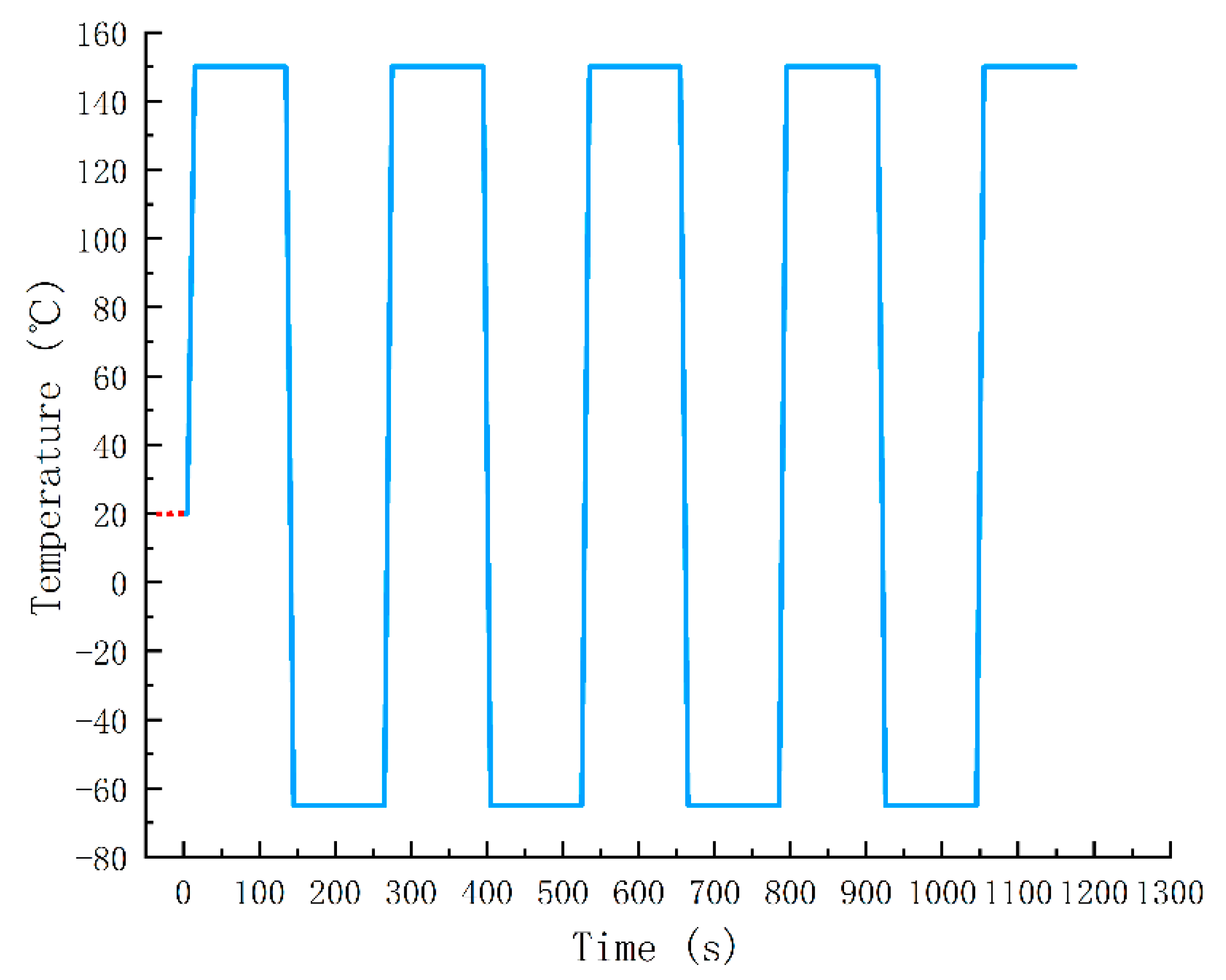
2. Experimental Procedure

The 3D packaging memory device is a double-sided molded ball grid array (DSMBGA) device, in which the components are arranged on the top and bottom of the substrate to reduce the package size and to shorten the signal path of the device [22]. It is composed of BGA flip chip, resistor, capacitor, PCB board, epoxy resin, etc., in which SAC305 is used as the solder. Figure 1 illustrates an example of the 3D packaging memory device.
As shown in Figure 2, according to the standard GJB548B, the high and the low temperatures in the thermal shock test are set to 150 °C and −65 °C, respectively. The switch time and the residence time are 10 s and 2 min, respectively. This means that one fatigue cycle is 250 s. After 800 cycles, the 3D packaging memory device is electrically tested at the room temperature. If the failure occurs, sample preparation will be carried out. Otherwise, the thermal shock test is repeated for 100 times, and then the electrical test is subsequently carried out until the device fails.
After the thermal shock test, the surface of the device sample is inspected by the metallographic microscope to observe whether there is deformation. According to the IPC-TM-650 test method, the sample is polished by a polishing machine to remove its surface coating and internal epoxy resin until the defective solder joint is exposed. The number of polished meshes ranges from 500 to 1000. Then, the sample is further polished by the soft polishing cloth and the diamond abrasive, in which the rotating speed is controlled at the speed of 100–200 RPM and the downward pressure is controlled below 351.5 g/cm2. After polishing, we dried the sample and observed its cross-section by means of a metallographic microscope (Nikon LV150). To protect and store the sample for a long period and to prevent external factors from damaging the sample (especially its solder joints), the sample is cast and inlaid by a metallographic sample inlaying machine. The sample is fixed by the epoxy resin. After the epoxy resin cures, the epoxy resin layer of the sample is polished by the above operations. To improve the picture definition acquired by the electron microscope, its surface is gilt to improve its electroconductivity. Finally, the micromorphology of the cross-section of the sample is observed by the SEM (EM-30 plus, COXEM). The accelerating voltage of the electron microscope is set to 15 kV and the distance between the lens and the sample is 13.5 mm.

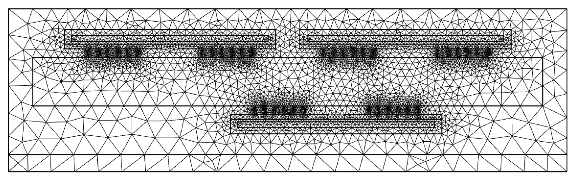
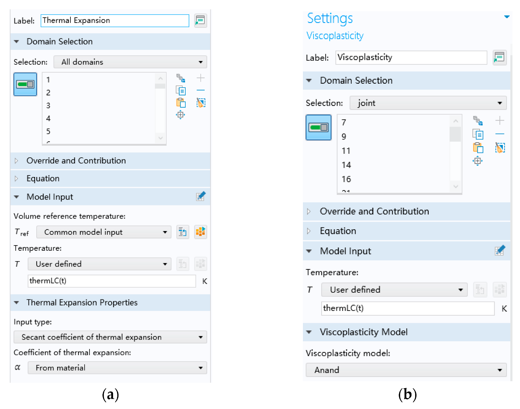
3. Finite Element Analysis

In order to analyze the failure mechanism of the sample under thermal shock, finite element analysis was performed on the 3D packaging memory device to simulate its stress-strain behavior under thermal shock.
In the thermal shock test, the SAC305 solder material follows the nonlinear behavior of the Anand material, whose model is defined as [23]:
ε p = A e x p Q R T sin h ζ σ S 1 / m
S a = S 0 ε p e x p Q R T n
S a = h 0 1 S a S a a s i g n 1 S a S a ε p  
In (1), ε p is inelastic strain rate, σ is equivalent stress, T is absolute temperature, A is viscoplastic rate coefficient (Pre-exponential factor), Q is activation energy, R is gas constant, ζ is stress multiplier, S is deformation impedance, and m is stress sensitivity. In (2) and (3), h 0 is hardening constant, S 0 is coefficient for deformation resistance saturation, S a is coefficient for deformation resistance saturation, and n is sensitivity for deformation resistance.
Because of the complex structure of the 3D packaging memory device, a simplified two-dimensional finite element model is used to speed up the calculation. Figure 3a shows the cross-section of the device observed by the metallographic microscope. Figure 3b shows the finite element model of the device.
As illustrated in Figure 4, the model of the device is meshed, in which the physics-controlled mesh is selected as the sequence type and the mesh size is fine so as to balance the calculation speed and accuracy.
To simulate the deformation of the device under thermal shock, the thermal expansion module is involved in its finite element model. In the thermal expansion simulation, all domains are selected for Domain Selection and the temperature function shown in Figure 2 is imported into the temperature model. In addition, the viscoplastic module is involved in the model, in which the Anand model is selected. Additionally, solder joints are selected for Domain Selection in the viscoplastic module, and the temperature function shown in Figure 2 is imported into the temperature model. These settings of the thermal expansion module and the viscoplasticity module are shown in Figure 5.
As illustrated in Figure 6, the constraint of the roller is imposed on the lowest layer of the device. After the settings of finite element model are completed, the finite element analysis is conducted with the time dependent. Specifically, the range (0, 5, 1185) is selected for Output times. That is, the calculation starts from 0 s, the results are output after each 5 s, and the calculation ends after 1185 s.
Figure 7a,b shows the distributions of von Mises stress for the solder joints of the device at the temperatures of −55 °C and 125 °C, respectively. Figure 7c shows the creep strain distribution after three simulated thermal shocks. In Figure 7, the chip at the upper left corner is labelled as Chip A, with the three solder joints on the left denoted as A1 and those on the right denoted as A2. Similarly, Chip B with B1 and B2 solder joints and Chip C with C1 and C2 solder joints are denoted in Figure 7. As illustrated in Figure 7, the plastic work and the creep strain are mostly distributed at the corner solder bump of the device. This means that the first crack initiation and the growth possibly occur at the solder corner of the device, because the thermomechanical failure of the solder joint is mainly caused by the accumulation of elastic strain. Figure 7c shows the cumulative equivalent creep strain after 5 thermal loading cycles. As shown in Figure 7c, plastic work and creep strain are accumulated at the chip side interface of the corner solder bump, which indicates that the locations near the chip side solder bump have the highest possibility of crack initiation and growth. Especially, the rightmost solder joint in C2 is imposed by the maximal stress and creep, which is located at the area with the maximal strain. Thus, it is regarded as a critical solder joint. The points at the upper right corner and the lower left corner are taken as critical point 1 and critical point 2, respectively. This is consistent with the experimental results. Therefore, it can be inferred that the main factors affecting the thermal reliability of the 3D packaging memory device are similar to those for typical electronic devices. The thermal stress is introduced into the device due to the differences of elastic and CTE between the components. Although the thermal stress is not high, the solder undergoes significant inelastic strain. The highest solder strain occurs in the solder of the lower chip since the shear stress plays an important role in the equivalent creep strain in this layer. Due to acute corner modeling, the edges of the solder joint have slightly high stresses. If the fillet corner modeling is substituted for acute corner modeling, the corresponding stresses will be slightly low. It is noted that the location of the maximum stress is consistent with the crack path in practical application.
Figure 8 shows the equivalent creep strain and shear creep strain components at the two critical points of the device. As indicated in Figure 8, the creep of the solder joint increases with time. When the temperature changes sharply, the creep increase rate of the solder joint becomes fast. When the temperature remains unchanged, the creep of the solder joint increases slowly.

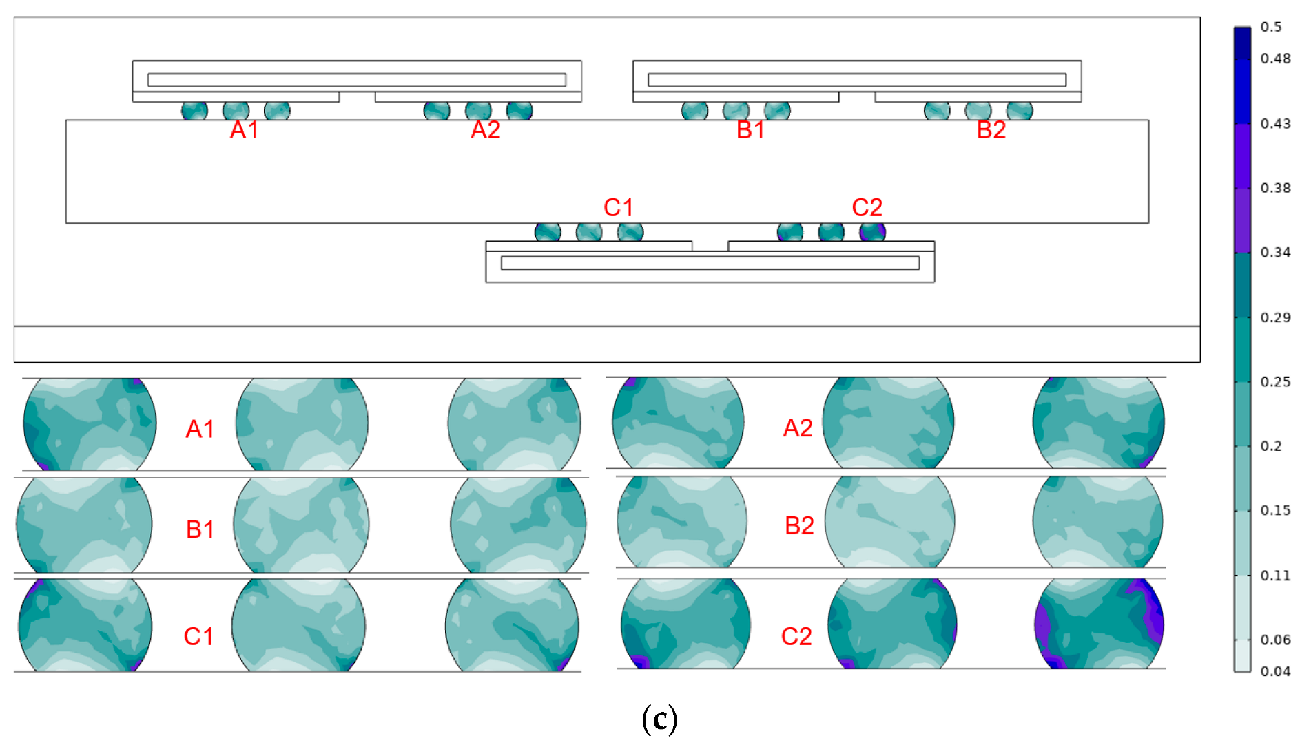
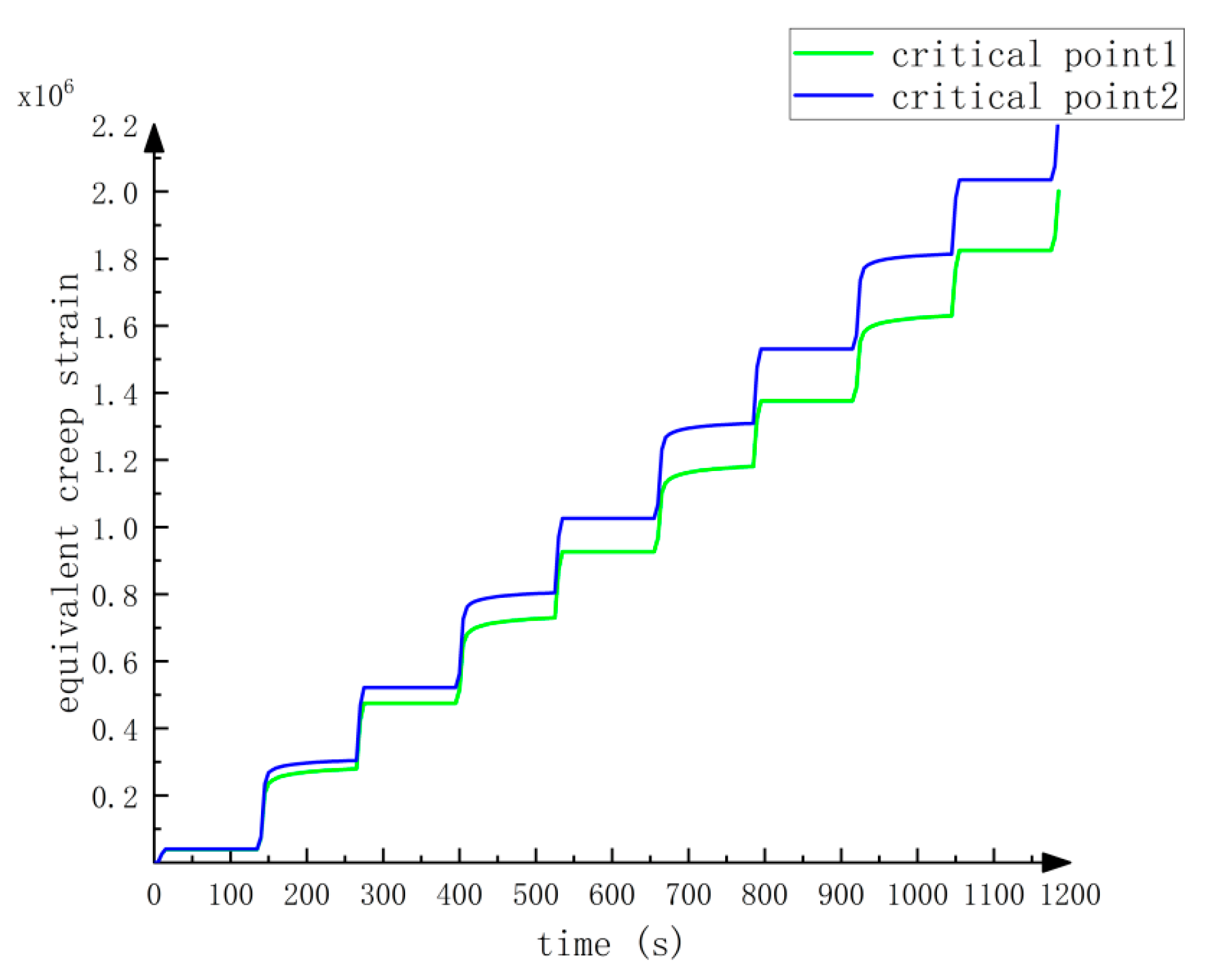
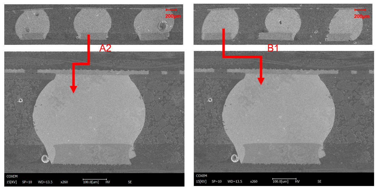
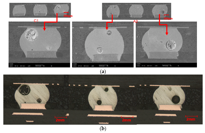
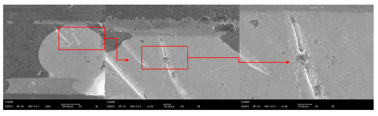
4. Results and Discussions

In order to study the microstructure changes during the thermal shock test, a cross-sectional study is carried out inside the 3D packaging memory device. Figure 9 shows the SEM micrographs of cross-sections of the solder joints among A2 and B1 solder joints, which are not damaged or subtly damaged after 1400 thermal shocks. It can be seen that parts of solder bumps have good shapes and are firmly bonded to the metallized PCB side of the bumps and the chip coating. There are some small defects on the edge of the solder joint. Additionally, a small number of cracks or crack initiation emerge on the edge of the solder joint, while there is no large void inside the solder joint.
Figure 10 illustrates the SEM micrographs of cross-sections of the solder joints among A2 and C1 solder joints, which are damaged after 1400 thermal shocks. As shown in Figure 10, there is a void in each solder joint, whose diameter is 120–140 μm. Voids are caused by the amount of outgassing flux entrapped in the solder joint during reflow [24]. Voids larger than 50% of the solder joint area will lead to potential reliability problems, resulting in a 25–50% reduction of the solder joint life in the mechanical test [25]. Notably, when several small voids emerge on one side, they will affect the reliability of the solder joint. Additionally, the location of the void influences the life of the solder joint. Specifically, if the void is located on the component side of the solder joint, it may accelerate the failure due to the reduction of the crack growth distance. With the increase of the number of thermal shock tests, the crack will grow inward in various directions.
The soldering position shift occurs at the inner edge of the C2 area in the device, resulting in a small contact area between the solder joint and the copper sheet. As observed by the electron microscope, many large cracks emerge in the solder joint, which are distributed at the corner solder bumps between the chip side and the packaging side. As shown in Figure 11, cracks or dents emerge on both sides of the solder joint. The cracks can be found near the interface between the solder joint and the PCB and grow to almost the entire cross-section of the solder joint through the void inside the solder joint. The maximal length of the crack exceeds 0.3 mm.
During thermal shock, β-Sn particles and Ag3Sn particles inside the SAC305 recrystallize and continuously coarsen, respectively [26]. When these particles appear in the recovery phase to form β-Sn sub-grain boundary, crack initiation possibly occurs. β-Sn particles expand to the whole solder joint under the stress, which provides a favorable path for crack growth [27,28]. During the procedure of thermal shock, the solder will creep through atomic diffusion and lattice slippage, which results in defects (such as voids and crack) at the solder [29]. Repeated stresses eventually lead to the formation and growth of interfacial cracks due to the combined damage mechanism of fatigue and creep [30]. Additionally, since the solder joint is affected by both shear stress and temperature, the plastic deformation gradually accumulates inside the solder alloy until the cracks appear [31]. Furthermore, there is a large difference between the CTEs of the epoxy resin and plastic encapsulant inside the chip and the solder joint (the solder joint CTE is 21 × 10−6 1/K, epoxy resin CTE is 67.1 × 10⁻⁶ 1/K and plastic encapsulant CTE is 17.68 × 10⁻⁶ 1/K) [32], which results in the solder enduring a large stress to accelerate crack growth for eventual crack [33]. It is found out that the crack grows earlier in the solder alloy than in the SAC305/Cu interface. The fact indicates that the solder alloy is prone to damage. Although cracks in the solder joint usually grow along the intermetallic compound layer, the cracks in epoxy filled chips grow in the oblique rather than horizontal directions due to the stress imposed by the epoxy on the solder joint during thermal shock. The fact is consistent with the simulations.

5. Conclusions

In this paper, we evaluate the reliability of 3D packaging memory devices under thermal shock by means of experimental observation and finite element analysis. In the thermal shock test, voids and cracks are the main factors to induce the fatigue failure of the solder joint, although the interface delamination failure possibly emerges. We simulate the 3D packaging memory device by means of finite element analysis to study its thermal behavior and its thermal performance. A simplified equivalent model is employed to speed up the simulation calculation. The simulated results indicate that cracks and voids are caused by the accumulation of plastic work and creep strain. The CTE difference between the epoxy resin and the solder joint speeds up the time of crack failure. Experimental results indicate that thermal fatigue failure will occur when the 3D packaging memory device encounters a sharp temperature change. Additionally, the non-elastic strain accumulation mainly affects the crack initiation and growth time. Although the structure of the 3D packaging memory device ensures its working ability in extreme environments, some failure behaviors of the 3D packaging memory device are different from those of 2D IC packaging devices. These failure behaviors involve larger voids and less cracks compared to those of 2D IC packaging devices. Our work introduces an experimental and simulated method to evaluate the reliability of the 3D packaging memory device under thermal shock, which can provide practical advice to guide optimizing the structure of the 3D packaging memory device and provides preventive maintenance suggestions. Additionally, our work is beneficial for the reduction of the design cycle of the device.

Author Contributions

Conceptualization, S.Z. and Z.L.; methodology, S.Z., Z.L. and H.W.; software, Z.L.; validation, S.Z. and Z.L.; formal analysis, S.Z. and Z.L.; investigation, S.Z. and Z.L.; resources, S.Z.; data curation, S.Z. and Z.L.; writing—original draft preparation, Z.L.; writing—review and editing, S.Z., Z.L., J.X., B.Z., Y.P., R.H., Y.B. and C.H.; visualization, S.Z. and Z.L.; supervision, S.Z., H.W., B.Q. and N.C.; project administration, S.Z., B.Q. and N.C.; funding acquisition, S.Z., B.Q. and N.C. All authors have read and agreed to the published version of the manuscript.

Funding

This work was in part supported by the National Natural Science Foundation of China (No. 62171142 and 61901123), the Key Laboratory Construction Projects in Guangdong (No. 2017B030314178), the Research Fund for Colleges and Universities in Huizhou (No. 2019HZKY003), the Project of Jihua Laboratory (No. X190071UZ190) and the National Natural Science Foundation of Guangdong Province, China (No. 2021A1515011908).

Conflicts of Interest

The authors declare no conflict of interest.

References

  1. Tian, W.; Ma, T.; Liu, X. TSV Technology and high-energy heavy ions radiation impact review. Electronics 2018, 7, 112. [Google Scholar] [CrossRef]
  2. Li, T.; Hou, J.; Yan, J.; Liu, R.; Yang, H.; Sun, Z. Chiplet heterogeneous integration technology—Status and challenges. Electronics 2020, 9, 670. [Google Scholar] [CrossRef]
  3. Hao, Y.; Xiang, S.; Han, G.; Zhang, J.; Ma, X.; Zhu, Z.; Guo, X.; Zhang, Y.; Han, Y.; Song, Z. Recent progress of integrated circuits and optoelectronic chips. Sci. China Inf. Sci. 2021, 64, 201401. [Google Scholar] [CrossRef]
  4. Lau, J.H. 3D IC Integration and 3D IC Packaging. In Semiconductor Advanced Packaging; Springer: Berlin/Heidelberg, Germany, 2021; pp. 343–378. [Google Scholar]
  5. Hu, X.; Stow, D.; Xie, Y. Die stacking is happening. IEEE Micro 2018, 38, 22–28. [Google Scholar] [CrossRef]
  6. Yu, M.; Fang, Y.; Wang, Z.; Chen, G.; Pan, Y.; Yang, X.; Yin, M.; Yang, Y.; Li, M.; Cai, Y. Encapsulation layer design and scalability in encapsulated vertical 3D RRAM. Nanotechnology 2016, 27, 205202. [Google Scholar] [CrossRef]
  7. Chakravarthi, V.S.; Koteshwar, S.R. Introduction to Design of System on Chips and Future Trends in VLSI. In SoC Physical Design; Springer: Berlin/Heidelberg, Germany, 2022; pp. 1–20. [Google Scholar]
  8. Jiao, J.; De, X.; Chen, Z.; Zhao, T. Integrated circuit failure analysis and reliability prediction based on physics of failure. Eng. Fail. Anal. 2019, 104, 714–726. [Google Scholar] [CrossRef]
  9. Yang, B.; Li, D.; Yang, H.; Hu, Y.; Yang, P. Vibrational fatigue and reliability of package-on-package stacked chip assembly. Microelectron. J. 2019, 92, 104609. [Google Scholar] [CrossRef]
  10. Qiu, B.; Xiong, J.; Wang, H.; Zhou, S.; Yang, X.; Lin, Z.; Liu, M.; Cai, N. Survey on Fatigue Life Prediction of BGA Solder Joints. Electronics 2022, 11, 542. [Google Scholar] [CrossRef]
  11. Depiver, J.A.; Mallik, S.; Amalu, E.H. Thermal fatigue life of ball grid array (BGA) solder joints made from different alloy compositions. Eng. Fail. Anal. 2021, 125, 105447. [Google Scholar] [CrossRef]
  12. Clech, J.-P.M.; Coyle, R.J.; Arfaei, B. Pb-free solder joint thermo-mechanical modeling: State of the art and challenges. JOM 2019, 71, 143–157. [Google Scholar] [CrossRef]
  13. Zhang, S.; Li, Z.; Zhou, H.; Li, R.; Wang, S.; Paik, K.-W.; He, P. Recent Prospectives and Challenges of 3D Heterogeneous Integration. e-Prime-Adv. Electr. Eng. Electron. Energy 2022, 2, 100052. [Google Scholar]
  14. Wang, C.; Huang, X.-J.; Vafai, K. Analysis of hotspots and cooling strategy for multilayer three-dimensional integrated circuits. Appl. Therm. Eng. 2021, 186, 116336. [Google Scholar] [CrossRef]
  15. Wen, Y.; Chen, C.; Ye, Y.; Xue, Z.; Liu, H.; Zhou, X.; Zhang, Y.; Li, D.; Xie, X.; Mai, Y.W. Advances on thermal conductive epoxy-based composites as electronic packaging underfill materials—A review. Adv. Mater. 2022, 2201023. [Google Scholar] [CrossRef] [PubMed]
  16. Jeong, H.; Jung, K.-H.; Lee, C.-J.; Min, K.D.; Myung, W.-R.; Jung, S.-B. Effect of epoxy mold compound and package dimensions on the thermomechanical properties of a fan-out package. J. Mater. Sci. Mater. Electron. 2020, 31, 6835–6842. [Google Scholar] [CrossRef]
  17. Deshpande, A.; Jiang, Q.; Dasgupta, A.; Becker, U. Impact of Interfacial Roughness on Tensile vs. Shear Creep Rupture of Solder Joints. In Proceedings of the 2021 20th IEEE Intersociety Conference on Thermal and Thermomechanical Phenomena in Electronic Systems (iTherm), San Diego, CA, USA, 1–4 June 2021; pp. 968–971. [Google Scholar]
  18. Schwerz, R.; Roellig, M.; Wolter, K.-J. Reliability analysis of encapsulated components in 3D-circuit board integration. In Proceedings of the 2018 19th International Conference on Thermal, Mechanical and Multi-Physics Simulation and Experiments in Microelectronics and Microsystems (EuroSimE), Toulouse, France, 15–18 April 2018; pp. 1–12. [Google Scholar]
  19. Chen, Y.; Jing, B.; Li, J.; Jiao, X.; Hu, J.; Wang, Y. Failure analysis and modeling of solder joints in BGA packaged electronic chips. IEEE Trans. Compon. Packag. Manuf. Technol. 2020, 11, 43–50. [Google Scholar] [CrossRef]
  20. Fan, J.; Wu, J.; Jiang, C.; Zhang, H.; Ibrahim, M.; Deng, L. Random voids generation and effect of thermal shock load on mechanical reliability of light-emitting diode flip chip solder joints. Materials 2019, 13, 94. [Google Scholar] [CrossRef]
  21. Han, Z.; Huang, X. GA-BP in thermal fatigue failure prediction of microelectronic chips. Electronics 2019, 8, 542. [Google Scholar] [CrossRef]
  22. Ghaffarian, R. Assembly Reliability of 3D Stacks under Thermal Cycles. In Proceedings of the 2020 19th IEEE Intersociety Conference on Thermal and Thermomechanical Phenomena in Electronic Systems (ITherm), Orlando, FL, USA, 26–29 May 2020; pp. 1152–1159. [Google Scholar]
  23. Xu, Y.; Zeng, Q.; Wang, Y.; Wu, M.; Chen, X.; Chen, G. The Discussion About the Identification of the Anand Model Parameters and Two Alternative Identification Methods. J. Electron. Packag. 2022, 145, 011205. [Google Scholar] [CrossRef]
  24. Yeo, S.M.; Yow, H.K.; Yeoh, K.H. Solder void size reduction in semiconductor package by vacuum reflow and pressure cure processes. Solder. Surf. Mt. Technol. 2022, 34, 239–254. [Google Scholar] [CrossRef]
  25. Pin, S.; Gracia, A.; Delétage, J.-Y.; Fouquet, J.; Fremont, H. Robustness of BGAs: Parametric study of voids’ distribution in SAC solder joints. Microelectron. Reliab. 2019, 102, 113484. [Google Scholar] [CrossRef]
  26. Belyakov, S.; Coyle, R.; Arfaei, B.; Xian, J.; Gourlay, C. Microstructure and damage evolution during thermal cycling of Sn-Ag-Cu solders containing antimony. J. Electron. Mater. 2021, 50, 825–841. [Google Scholar] [CrossRef]
  27. Gu, J.; Lin, J.; Lei, Y.; Fu, H. Experimental analysis of Sn-3.0 Ag-0.5 Cu solder joint board-level drop/vibration impact failure models after thermal/isothermal cycling. Microelectron. Reliab. 2018, 80, 29–36. [Google Scholar] [CrossRef]
  28. Gain, A.K.; Zhang, L. Thermal aging effects on microstructure, elastic property and damping characteristic of a eutectic Sn–3.5 Ag solder. J. Mater. Sci. Mater. Electron. 2018, 29, 14519–14527. [Google Scholar] [CrossRef]
  29. Wu, P.; Wang, P.; Chiang, K. Empirical solutions and reliability assessment of thermal induced creep failure for wafer level packaging. IEEE Trans. Device Mater. Reliab. 2018, 19, 126–132. [Google Scholar] [CrossRef]
  30. Li, Q.-H.; Li, C.-F.; Zhang, W.; Chen, W.-W.; Liu, Z.-Q. Microstructural evolution and failure mechanism of 62Sn36Pb2Ag/Cu solder joint during thermal cycling. Microelectron. Reliab. 2019, 99, 12–18. [Google Scholar] [CrossRef]
  31. Chen, Y.; Wang, C.; Gao, Y.; Gao, Z.; Liu, Z.-Q. Microstructural evolution and failure analysis of Sn–Bi57–Ag0. 7 solder joints during thermal cycling. J. Mater. Sci. Mater. Electron. 2022, 33, 1942–1952. [Google Scholar] [CrossRef]
  32. Depiver, J.A.; Mallik, S.; Harmanto, D. Solder joint failures under thermo-mechanical loading conditions—A review. Adv. Mater. Process. Technol. 2021, 7, 1–26. [Google Scholar] [CrossRef]
  33. Liu, D.; Pons, D.J. Crack propagation mechanisms for creep fatigue: A consolidated explanation of fundamental behaviours from initiation to failure. Metals 2018, 8, 623. [Google Scholar] [CrossRef]
Figure 1. 3D packaging memory device.
Electronics 11 02556 g001
Figure 2. Schematic representation of the thermal cycling.
Electronics 11 02556 g002
Figure 3. 3D packaging memory device under thermal shock. (a) Its cross-section observed by the metallographic microscope; (b) its finite element model.
Electronics 11 02556 g003
Figure 4. Meshing of 3D packaging memory.
Electronics 11 02556 g004
Figure 5. The settings of (a) thermal expansion module; (b) viscoplasticity module.
Electronics 11 02556 g005
Figure 6. The settings of (a) boundary constraint; (b) finite element analysis.
Electronics 11 02556 g006
Figure 7. Contour maps of the von Mises stress and Creep strain of the solder joint under thermal shock. (a) von Mises stress at −55 °C; (b) von Mises stress at 125 °C; (c) creep strain.
Electronics 11 02556 g007aElectronics 11 02556 g007b
Figure 8. Creep strain development at a critical point.
Electronics 11 02556 g008
Figure 9. Diagonal cross-sectional SEM images of the solder joints after thermal shocks.
Electronics 11 02556 g009
Figure 10. Diagonal cross-sectional (a) SEM and (b) metallographic microscope images of the solder joints after thermal shocks.
Electronics 11 02556 g010
Figure 11. Diagonal cross-sectional 260×,1000× and 2000× SEM images of the solder joint which has large cracks after thermal shocks.
Electronics 11 02556 g011
Publisher’s Note: MDPI stays neutral with regard to jurisdictional claims in published maps and institutional affiliations.

