Article

Oxide Electric Field-Induced Degradation of SiC MOSFET for Heavy-Ion Irradiation

1
Key Laboratory of Functional Materials and Devices for Special Environments, Xinjiang Technical Institute of Physics and Chemistry, Chinese Academy of Sciences, Urumqi 830011, China
2
University of Chinese Academy of Sciences, Beijing 100049, China
*
Authors to whom correspondence should be addressed.
Electronics 2023, 12(13), 2886; https://doi.org/10.3390/electronics12132886
Submission received: 31 May 2023 / Revised: 19 June 2023 / Accepted: 27 June 2023 / Published: 29 June 2023
(This article belongs to the Special Issue Radiation Effects of Advanced Electronic Devices and Circuits)

Abstract

:
This work presents an experimental study of heavy-ion irradiation with different particle linear energy transfer (LET), gate biases, and drain biases. The results reveal that when the irradiation biases are low, the SiC MOSFET does not experience single event effect (SEE) and the electrical properties remain unchanged (the devices are in the safe operating area (SOA)). However, the oxide breakdown voltage of the device is significantly decreased due to the latent damage generated by the irradiation. The experimental results, along with TCAD simulations, suggest that the latent damage induced by the irradiation in the gate oxide is closely related to the peak electric field in the gate oxide at the time of particle incidence. This peak electric field is determined by the potential difference between the two sides of the gate oxide, which is affected by the particle LET, gate biases, and drain biases together. The high potential is determined by the combined effect of the LET and the drain-source voltage. The impact ionization of the particle by the applied electric field causes the accumulation of holes in the JFET oxide, which leads to a decrease in the doping of the N epitaxial layer and eventually causes a rise in the high potential near the JFET oxide. The low potential is determined by the gate bias, and the negative bias applied to the gate can further increase the potential difference between the two sides of the oxide, causing an increase in the peak electric field in the gate oxide and aggravating the gate oxide damage.

1. Introduction

Silicon carbide (SiC) MOSFETs are a new generation of power devices based on wide bandgap semiconductor materials with excellent high-voltage, high-temperature, and high-frequency characteristics. SiC MOSFETs can significantly improve system efficiency and power density while reducing system size and weight and have gained widespread attention and application in various fields, including for electric vehicles, high-voltage power grids, photovoltaic inverters, and railroad traction [1,2,3]. Furthermore, there is a growing demand for new power devices with high performance and high reliability in aerospace, nuclear power, and other radiation fields [4,5]. However, the performance of Si-based power devices has reached its physical limit and cannot be further enhanced; thus, researchers have also turned their attention to SiC power devices. Rays and particles in the radiation environment can affect the characteristics of SiC power devices and pose a threat to the performance and reliability of the devices; therefore, there is an urgent need to investigate the radiation effect and reliability degradation mechanisms of SiC MOSFETs in the radiation environment [6].
Because of the thick gate oxide, power MOSFETs are susceptible to the total ionizing dose (TID) effects in the space radiation environment, causing the degradation of electrical parameters such as the threshold and blocking voltages [7,8]. In addition, the power devices are sensitive to single-event effects due to the high-rated drain voltage and ease of particles passing through the sensitive region of the device. The most severe challenges currently faced by SiC MOSFETs in the space radiation environment are single-event burnout (SEB) and single-event gate rupture (SEGR) caused by high-energy particles [9,10,11,12,13,14,15,16]. Single-event effects can lead to the instantaneous catastrophic failure of the device, impacting the reliability of the spacecraft. To ensure the reliability of SiC MOSFETs in space applications, high-energy particle irradiation experiments are conducted on the devices to determine their failure threshold voltage and establish the SEE safe operating area for devices [6,17]. It has been demonstrated that the safe operating area of SiC MOSFETs under heavy-ion irradiation is closely correlated to VDS, as illustrated in Figure 1 [18,19]. In Region 3, high VDS was applied during heavy-ion irradiation, and SEB occurred in the device [11]. At this stage, the PN junction between the source and drain burnt out, and the device lost the blocking characteristics. In Region 2, with medium VDS, damage or latent damage occurred in the source-drain PN junction and gate oxide of the SiC MOSFET. These damages caused a significant increase in the leakage current of the device, resulting in the degradation of the characteristics. It is worth noting that the increased gate-source leakage current IGSS in this region indicated that the device had undergone the SEGR effect. It was concluded that the oxide damage induced by heavy-ion irradiation could be attributed to multiple particle impacts [14,20], high electric fields generated by accumulated holes [21], or localized high-power density [15,19,22]. In Region 1, devices were irradiated at low VDS, the electrical parameters of the device did not change significantly, and the devices were considered to be in the safe operating area [6].
The above study found that the determination of the safe operating area for SiC MOSFETs in the space environment pertains to the effect of drain bias. However, SiC MOSFETs are high-voltage, high-power devices that typically require the application of negative gate voltage to prevent improper conductivity during operation. Therefore, the effect of gate bias (VGS) must also be considered when determining the safe operating area of the device through experiments. Moreover, the long-term reliability of devices in the safe operating area must be taken into account. The gate oxide reliability of SiC MOSFETs has been a significant concern [23,24]. Although the gate oxide reliability of SiC MOSFETs in conventional environments has been largely solved [25], the damage in the gate oxide caused by heavy-ion irradiation in region 2 has raised concerns regarding the long-term reliability of SiC MOSFETs in space radiation environments. Therefore, the variation of oxide reliability in the safe operating region must be further investigated.
In this study, heavy-ion irradiation experiments were conducted at low biases (both the VDS and VGS) to ensure that the devices operated within the safe operating area. The irradiated devices were subjected to accelerated stress experiments on gate oxide to obtain the changes in oxide reliability. Based on the experimental results, the effect of gate and drain bias on the oxide reliability is summarized, and the mechanism of the oxide damage is analyzed by combining the experimental results and TCAD simulation.

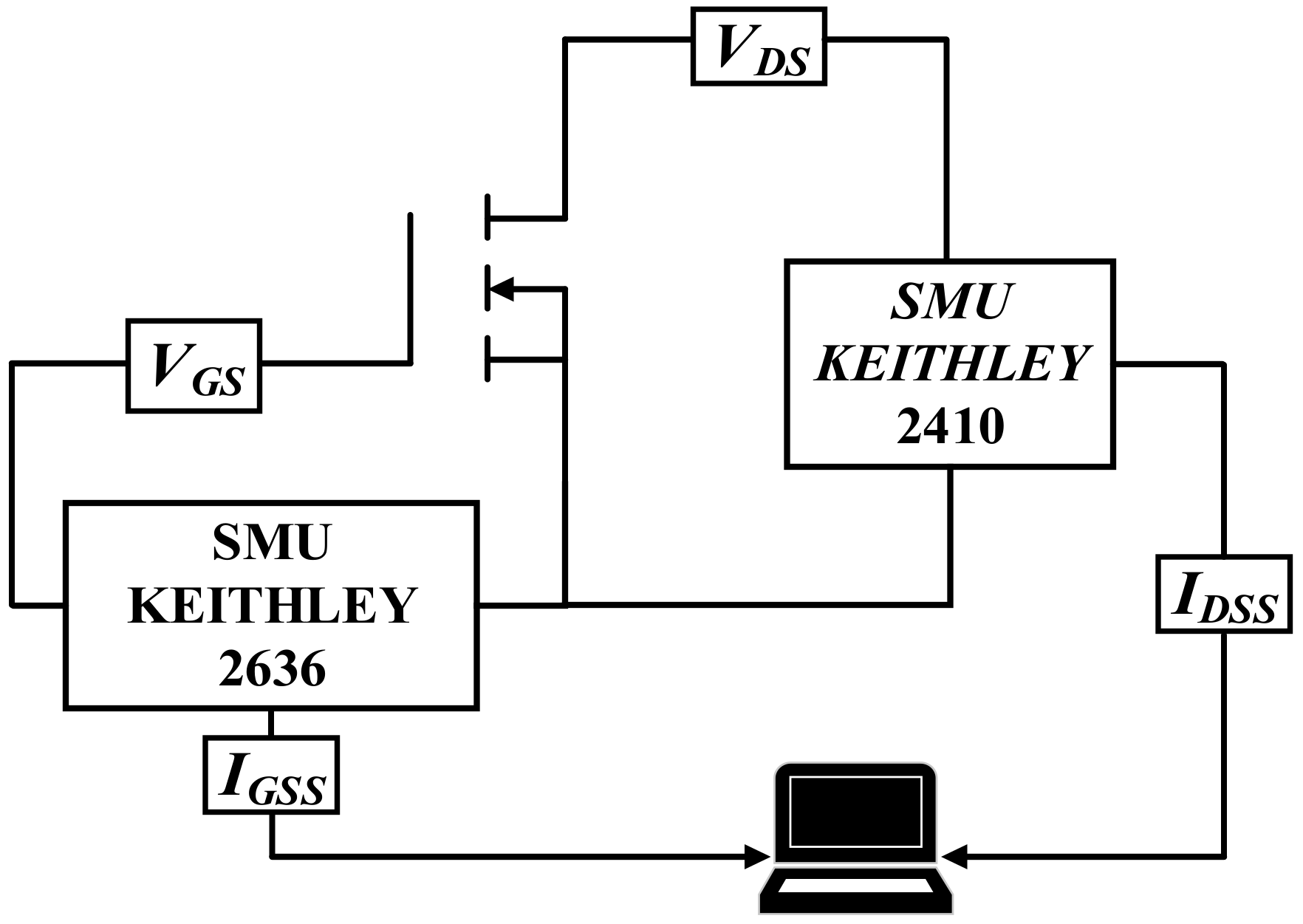
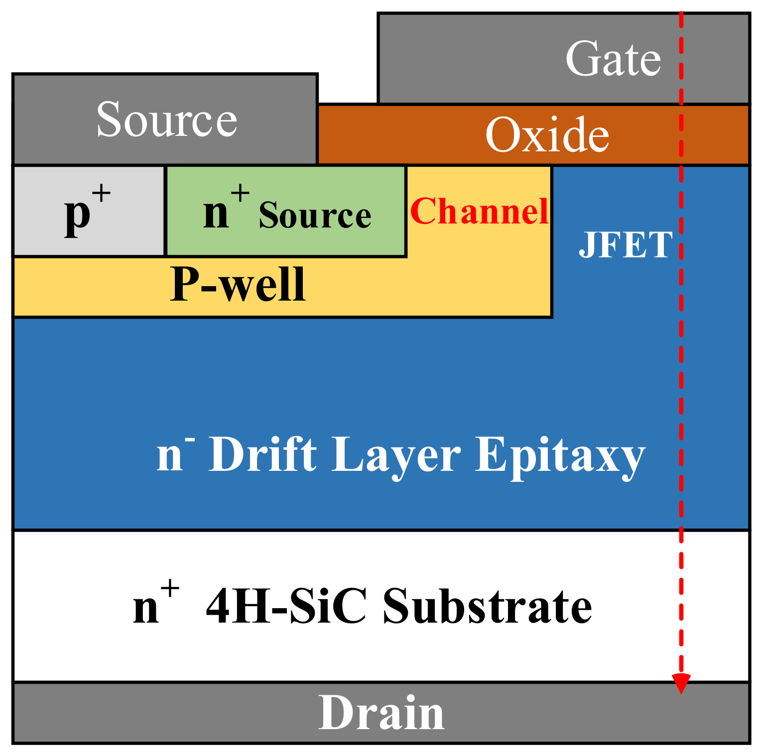
2. Experimental Setup

The devices under test (DUT) used in this study were commercial 1200 V, 60 mΩ N-channel SiC MOSFETs (CGE1M120060). The recommended gate-source voltage of the device was −5/+20 V and the measured drain-source breakdown voltage V(BR)DSS was approximately 1500 V (test condition was IDS = 1 mA). The thickness of the oxide layer was approximately 50 nm, and the thickness of the epitaxial layer was approximately 10 μm. The die of this device was selected to allow heavy ions to penetrate the sensitive region of the device. The die was encapsulated for the bias experiments. Heavy-ion irradiation experiments were conducted at the China Institute of Atomic Energy and the Lanzhou Heavy Ion Accelerator National Laboratory. The irradiated heavy ions were 35Cl, 73Ge, and 181Ta, and the corresponding LETs in SiC were 15.89, 39.6, and 78.7 MeV/(mg/cm2), respectively. The flux in the experiments was 1 × 10⁴ ions/cm2/s, and the fluence was 1 × 10⁶ ions/cm2. Low drain and gate biases were used to ensure that no single-event effect occurred in the device. The experimental configurations are shown in Table 1. The incidence depths of three ions in the device were greater than 20 μm, indicating that all could pass through the sensitive region (10 μm epitaxial layer); thus, the effect of incidence depth could be excluded in the subsequent analysis.
The Keithley Source Measure Unit models 2636 and 2410 were connected to a PC to record the changes in the gate-source leakage current (IGS) and drain-source leakage current (IDS) during irradiation in real time, and the connection is shown in Figure 2. In the test, the high-voltage Source Measure Unit model 2410 applied a drain-source voltage and monitored the leakage current at this voltage; the Source Measure Unit model 2636 applied a negative gate-source voltage to ensure channel shutdown and monitored the leakage current corresponding to this negative gate voltage in real-time. In order to ensure that the source meter would not be damaged during the experiment, the current limit of the source meter was set to 1 μA. Only one device could be irradiated at a time with this system, and to ensure the accuracy of the experimental results, three devices were irradiated for each bias condition (see Table 1).
The change in the subthreshold transfer characteristic curve of the SiC MOSFET was measured before and after irradiation using a Keithley 4200-SCS semiconductor parametric instrument. The I–V curve was tested with the drain voltage VDS = 50 mV, and the gate voltage swept from −5 V to 10 V. The blocking voltage of the device was measured using BC3193 at IDS = 1 mA. Heavy-ion irradiation can induce latent damage in the gate oxide as a precursor to oxide breakdown [14]. Some of the latent damage in oxide can be easily activated by the applied gate stress and cause oxide breakdown. Therefore, post-irradiation gate stress (PIGS) tests were conducted on the devices using Keithley 4200-SCS after irradiation. In the PIGS test, the gate-source voltage VGS was scanned from 0 V to 20 V, and the variation of the gate oxide leakage current IGSS was monitored.
Since the activation energy of the latent damage in the oxide is unknown, the PIGS test from 0 to 20 V did not guarantee the activation of the gate oxide latent damage to fully characterize the change in gate oxide reliability. Therefore, a ramp voltage stress (RVS) test with higher gate voltage was performed on the device. In the RVS test, the gate voltage started from 20 V and increased by 200 mV every 20 s until oxide breakdown occurred, and the gate voltage at the time of oxide breakdown was recorded. Both irradiation and tests were performed at room temperature.

3. Results and Analysis

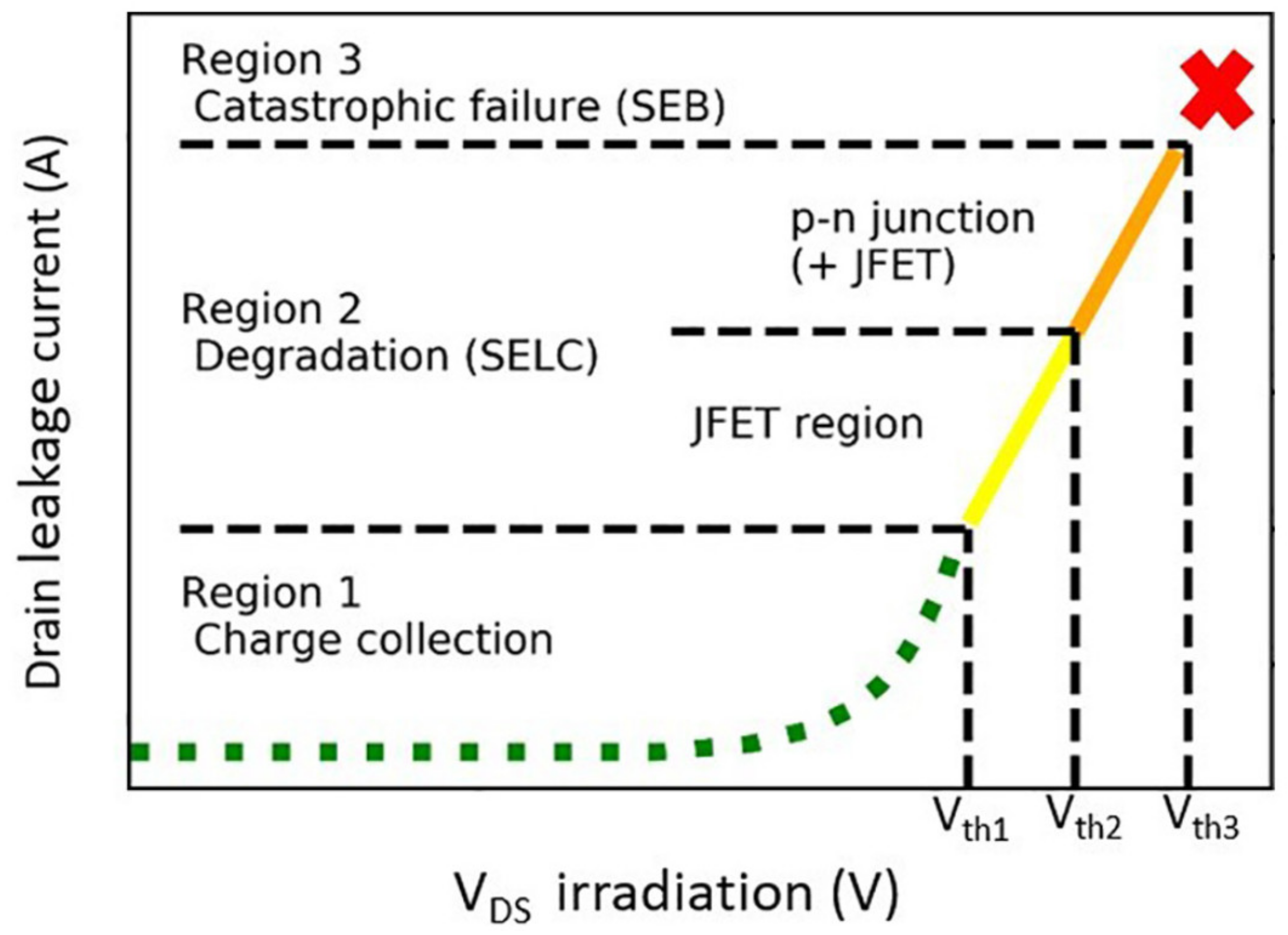
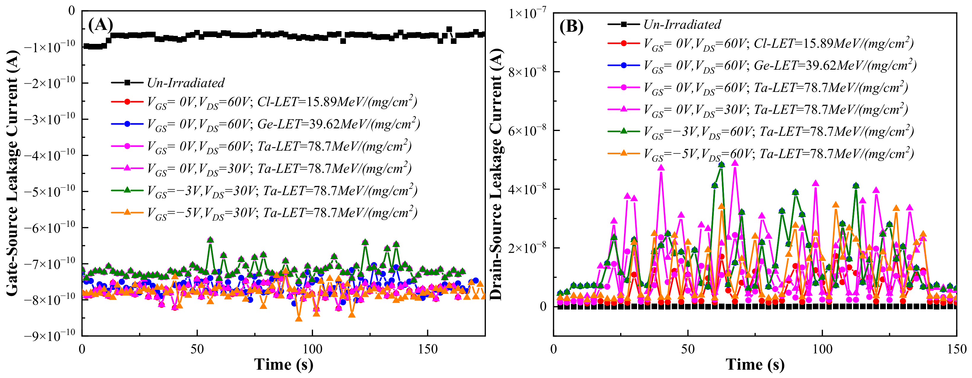
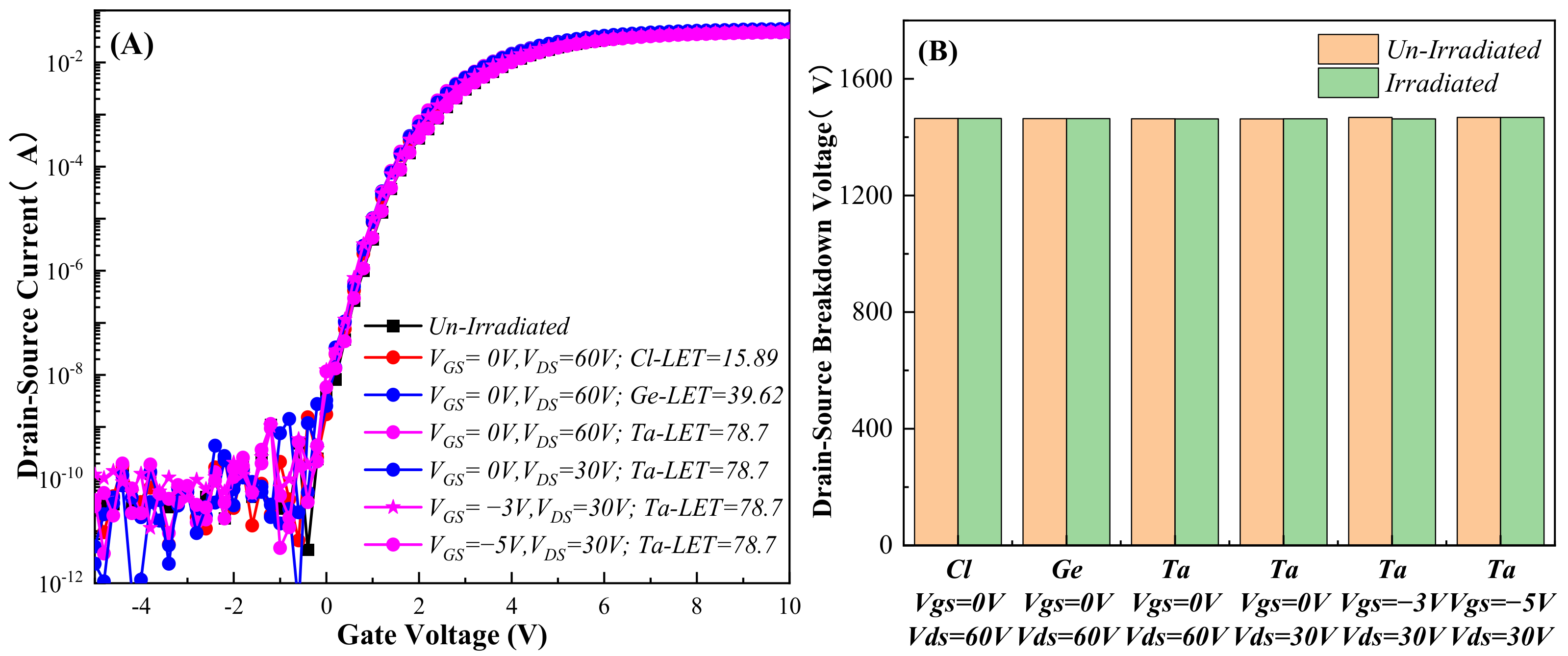
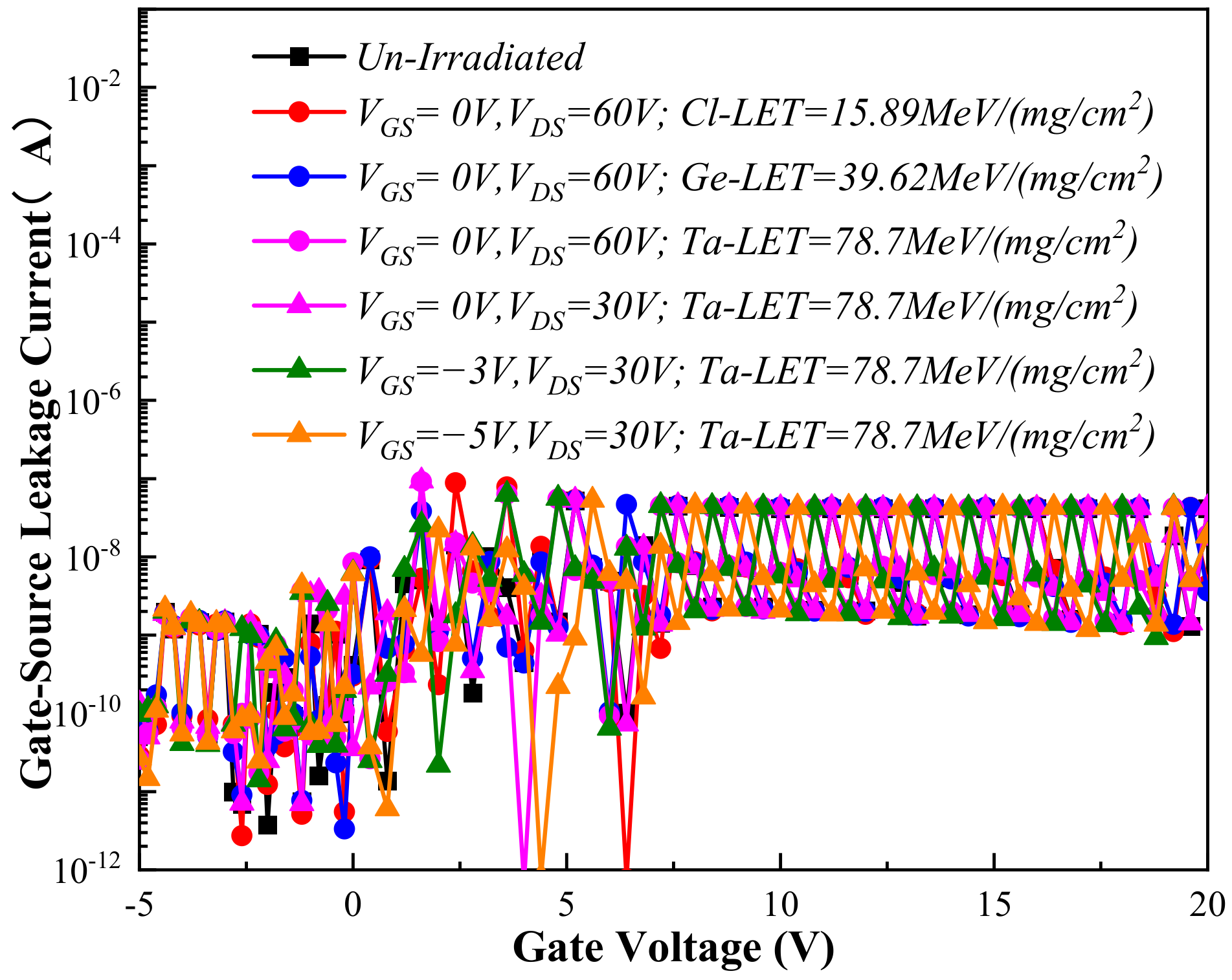
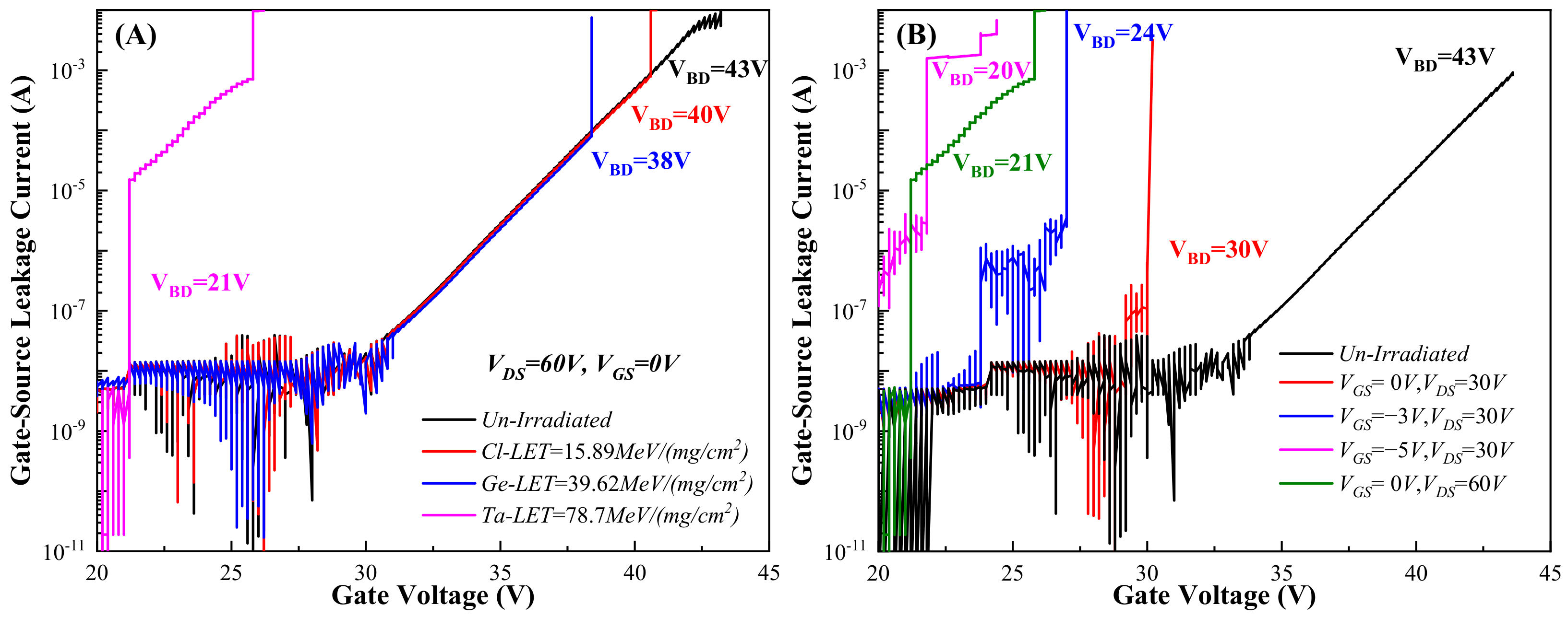
3.1. Heavy-Ion Experiment Results

During the heavy-ion irradiation test, biases were applied to the gate-source and drain-source terminals simultaneously. The variations of the gate-source leakage current (corresponding to VGS = 0 V, −3 V, and −5 V) and drain-source leakage current (corresponding to VDS = 30 V and 60 V) of the devices are shown in Figure 3. During the irradiation period, the leakage current jumped significantly, while after the irradiation ceased, the current no longer displayed significant jumps, and only minor fluctuations were observed. The analysis suggested that the jump in leakage current during irradiation was caused by the interaction between heavy ions and the extranuclear electron of the material. The high flux of heavy ions during irradiation generated a large number of electron-hole pairs within the material, leading to carrier fluctuations inside the material, which were ultimately manifested as jumps in the leakage current. This effect ceased after the irradiation was terminated, resulting in the current returning to its initial value.
The transfer characteristic curves of the SiC MOSFETs did not exhibit significant drift after irradiation, as depicted in Figure 4A. According to the maximum transconductance method, the threshold voltage of the device was extracted in the I–V curve, and the VTH of the device was approximately 2.4 V before and after irradiation, without significant changes. This indicated that the equivalent total ionizing dose produced by heavy-ion irradiation was low and did not accumulate trapped charges in the oxide of the device, causing a change in the threshold voltage. The change in the blocking voltage of the device before and after irradiation is shown in Figure 4B. The blocking voltage was approximately 1500 V, and no degradation occurred. This result indicates that heavy-ion irradiation does not produce significant defects in the SiC material that causes degradation of the reverse blocking characteristics of the PN junction composed of N-epitaxy and P-well.
The results of the PIGS test (0–20 V) of the irradiated devices under different conditions are depicted in Figure 5. The oxide leakage current of the irradiated device did not exhibit significant changes in comparison to the unirradiated device. This suggests that the irradiation biases used in the test were within the SEE SOA of the device. Although no SEGR occurred in the gate oxide of the device under these irradiation biases, the heavy-ion irradiation may have produced latent damage in the gate oxide that was difficult to activate. Therefore, the RVS experiments with higher gate voltage were continued for the device.
Figure 6A illustrates the changes in the oxide breakdown voltage of the device after heavy-ion irradiation with different LET at VGS = 0 V and VDS = 60 V. Figure 6B presents the degradation of the oxide breakdown voltage of SiC MOSFETs after irradiation with different gate and drain biases. It can be observed that as the LET, drain voltage, and gate voltage increased, the oxide breakdown voltage of the device degraded drastically.
The degradation of the oxide breakdown voltage in irradiated devices is suggested to be closely associated with the transient high electric field in the oxide during irradiation. The high electric field can cause a rapid rise in the generation rate of defects in SiO2 [26], resulting in a higher density of latent damage in the oxide. The latent damage does not affect the characteristics when it is not activated but can seriously affect the oxide reliability once activated.

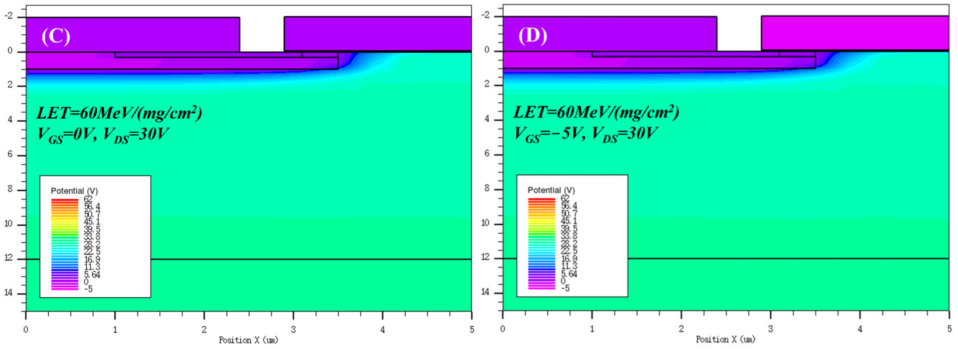
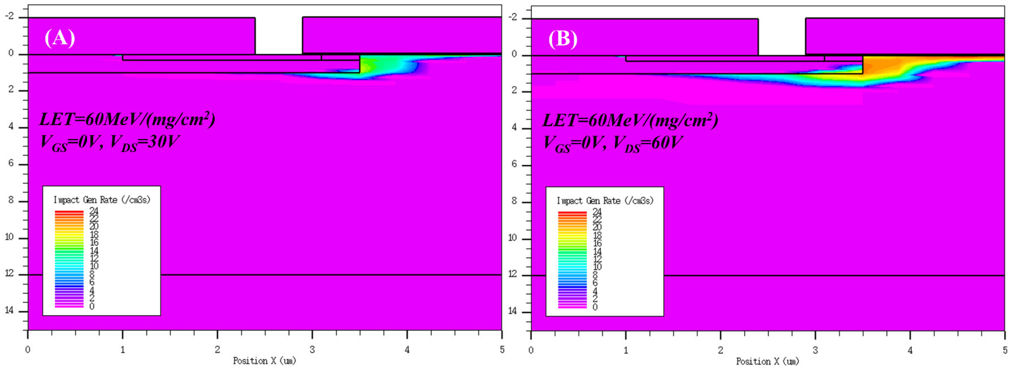
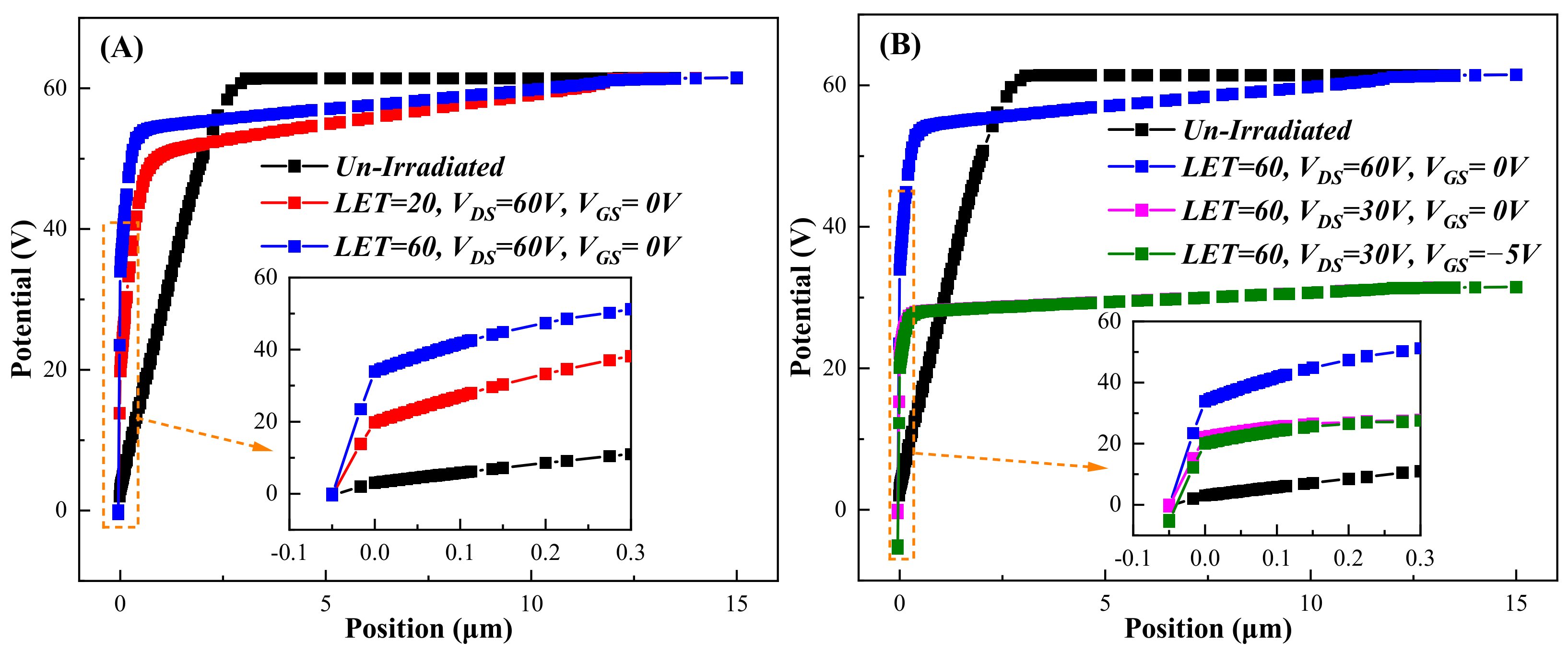
3.2. Degradation Mechanism of Oxide Reliability

The experimental results discussed above reveal that heavy-ion irradiation leads to a decrease in oxide breakdown voltage, influenced by the LET, gate bias, and drain bias. When heavy ions penetrate the device, a significant number of electron-hole pairs can be generated along its traces, affecting the carrier concentration in the device and, consequently, altering the potential distribution. Due to the extremely short response time of heavy-ion incidence, the instantaneous potential and field changes in the oxide could not be monitored experimentally using the equipment in the experiment. Therefore, TCAD simulations were used to analyze the electrical parameters at the moment of particle incidence.
The irradiated device used in this study was a planar gate SiC MOSFET, and the cross-section of the devices is depicted in Figure 7. Based on this structure, a two-dimensional model was constructed in TCAD. The simulation parameters were obtained from previously published papers [11,12,27,28], as shown in Table 2. In the simulation, the incident position of the heavy ions was located above the JFET region, which is the most sensitive area of the oxide. The heavy-ion incidence path is shown as the red dashed line in Figure 7, which penetrated through the gate oxide and epitaxial layer. The number of electron-hole pairs generated by the particle along its incident path was related to the LET, and unit conversion was required in the simulation: 1 pC/μm(SiC) = 151 MeV/mg/cm2. The electric field in the oxide reached its peak value of approximately 10 ps of ion incidence, followed by a rapid decrease in the electric field in the gate oxide. Hence, the distribution of potential barriers and electric fields at 10 ps for the irradiated device under different conditions was extracted during the simulation. The models used in the simulations included the drift-diffusion model for transport, the Shockley–Read–Hall model for generation-recombination, the doping dependence model, and a high field saturation model for mobility.
Heavy ions generate electron-hole pairs along their incident traces. The applied voltage during irradiation induces an electric field in the device, and the collisional ionization of carriers under the electric field produces a lot of electron-hole pairs. At the same time, the electrons and holes move in opposite directions under the action of the electric field. The electrons are more mobile than the holes in SiC [29]; this causes holes to move and accumulate at the SiC/SiO2 interface. As shown in Figure 8, the concentration of holes inside the device varies with LETs. Heavy ions with high LET result in a much higher hole concentration inside the device than the low LET particle. The analysis suggested that the irradiation bias was the same in both figures, indicating that the electric field inside the device was the same. However, the incident particle with high LET produced a higher number of electron-hole pairs along its path, leading to more intense carrier collision ionization, which, ultimately, makes a higher density of accumulated holes.
In general, SiC MOSFETs have low doping in the N-type epitaxial region to increase the blocking voltage. Therefore, the accumulated holes from heavy-ion irradiation can severely reduce the doping in the N-type epitaxial region near the incident path. The change in doping concentration further affects the potential distribution inside the device.
The simulations of potential distributions inside the device for different LETs are given in Figure 9A,B. The potential distribution near the JFET oxide is more intensive with high LET heavy ions. The analysis suggested that this was due to the high density of holes generated by the high LET heavy ions causing a reduction in N epitaxial doping near the JFET oxide. The doping of the N epitaxial region is closely related to the blocking characteristics of the device, and the drain voltage drops mainly in the depletion layer of the lower-doped N epitaxial region during the blocking state. Therefore, the reduced N doping near the JFET oxide led to a more intensive potential distribution near it.
Figure 9B,C show the simulated potential distribution in the device when irradiated at different VDS. The potential near the JFET oxide increased remarkably when irradiated with heavy ions at high VDS. The analysis suggested that the increase in high potential was closely related to the high electric field generated by the VDS. At the high electric field, the impact generation rate of the carriers increased, which generated more electron-hole pairs in the device. The simulations of the impact generation rate in irradiated devices at different VDS are depicted in Figure 10. The impact generation rate near the JFET oxide of the devices irradiated at high VDS was significantly higher than those irradiated at low VDS. The high impact generation rate could generate more electrons and holes. The accumulation of holes further decreased N doping near the JFET oxide, which also increased the potential.
A comprehensive analysis of the influence mechanisms of LET and VDS suggested that they jointly determine the high potential value on the SiC side of the JFET gate oxide layer at heavy-ion incidence.
Comparing Figure 9C,D, it is found that the potential distribution near the JFET oxide was approximately the same when irradiated at the same LET and drain bias. However, the negative gate bias could affect the low potential of the metal oxide. As the negative gate bias voltage increased, the low potential value on the metal side of the gate oxide decreased. The difference between the high and low potential values on both sides of the gate oxide determined the peak electric field in the oxide.
In order to provide a more intuitive analysis of the effects of LET, VDS, and VGS on the peak electric field in the gate oxide, the potential distribution along the particle trace was extracted in the simulation, and the results are shown in Figure 10. For the unirradiated device, the high voltage applied at the drain uniformly dropped in the epitaxial layer of approximately 3 μm. However, for the irradiated device, the drain bias experienced a significant drop near the gate oxide. By examining the enlarged plot in Figure 11A, it is evident that the LET mainly affected the high potential value on the SiC side of the gate oxide. The proportion of the drain voltage coupled to the oxide increased continuously with the increase in the LET. The simulation of the potential distributions in the irradiated device at different VDS and VGS are given in Figure 11B. The high potential of the gate oxide in the irradiated device at different VDS was significantly different, and the potential in the irradiated device at high VDS was much higher than that at low VDS. This discrepancy is mainly attributed to the intensified collisional ionization resulting from the high electric field at high VDS. The VDS and LET jointly affected the high potential of the gate oxide. There was no significant difference in the high potential of irradiated devices under different VGS, but the low potential varied with VGS. The potential difference between the high and low potentials determined the peak electric field in the gate oxide.
The gate oxide thickness of the device in the simulation was 50 nm, and, as can be concluded from Figure 11, the potential difference between the two sides of the gate oxide reached more than 20 V, even at a lower bias. Therefore, it can be calculated that the instantaneous peak electric field in the gate oxide was greater than 4 MV/cm, which was even close to the critical breakdown electric field of SiO2 (10 MV/cm) at higher VDS. The increase in the transient peak electric field greatly increased the defect generation rate, thus creating more defects in the gate oxide and affecting the reliability of the gate oxide.

4. Conclusions

This study investigated the effect of the peak electric field in the gate oxide on the generation of oxide latent damage during heavy-ion irradiation. The irradiated SiC MOSFETs were found to have no single-event effect and good functional characteristics, but the oxide reliability was degraded. The experimental results show that the degree of oxide reliability degradation is affected by a combination of LET, VGS, and, VDS.
The analysis and simulation concluded that the degradation of the oxide reliability of SiC MOSFETs is caused by the defects generated by the peak electric field during heavy-ion irradiation. The particle LET and VDS can affect the high potential coupled to one side of the gate oxide during irradiation, while the applied VGS affects the low potential on the other side of the oxide. The potential difference between the two determines the peak electric field in the gate oxide.
The results of this study suggest that even if irradiation biases are in the SEE safe operating area, heavy-ion irradiation can severely limit the reliability and lifetime of the device, which poses a new challenge for the space application of SiC MOSFETs. In summary, for the study of the adaptability of SiC MOSFETs in the space environment, in addition to the tricky SEE study of SiC MOSFETs, the gate oxide reliability must be considered.

Author Contributions

Methodology, X.L. and J.F.; Software, Y.W.; Validation, Y.L.; Investigation, D.Z.; Resources, X.Y. and Q.G.; Data curation, H.F. and Y.X.; Funding acquisition, J.S., J.F. and Y.W. All authors have read and agreed to the published version of the manuscript.

Funding

This work was partially funded by the National Natural Science Foundation of China (Grant no. 11975305 and 12175307) and Young Scholars in Western China, the Chinese Academy of Sciences (Grant no. 2021-XBQNXZ-021).

Data Availability Statement

Not applicable.

Acknowledgments

This work acknowledges the support of the Institute of modern physics, Chinese Academy of Sciences and the China institute of atomic energy in the heavy ion experiment.

Conflicts of Interest

The authors declare no conflict of interest.

References

  1. She, X.; Huang, A.Q.; Lucia, O.; Ozpineci, B. Review of Silicon Carbide Power Devices and Their Applications. IEEE Trans. Ind. Electron. 2017, 64, 8193–8205. [Google Scholar] [CrossRef]
  2. Roccaforte, F.; Fiorenza, P.; Greco, G.; Nigro, R.L.; Giannazzo, F.; Iucolano, F.; Saggio, M. Emerging Trends in Wide Band Gap Semiconductors (SiC and GaN) Technology for Power Devices. Microelectron. Eng. 2018, 187–188, 66–77. [Google Scholar] [CrossRef]
  3. Li, J.; Igarashi, S.; Fujishima, N. SiC Power Devices and Application to Power Electronics. In Proceedings of the PCIM Asia 2022, International Exhibition and Conference for Power Electronics, Intelligent Motion, Renewable Energy and Energy Management, Shanghai, China, 26–27 October 2022. [Google Scholar]
  4. Boomer, K.; Lauenstein, J.M.; Hammoud, A. Body of Knowledge for Silicon Carbide Power Electronics; NASA: Washington, DC, USA, 2016. [Google Scholar]
  5. Jie, X.; Qing, K.; Xuan, Z.; Feng, L. Application Prospect of SiC Power Semiconductor Devices in Spacecraft Power Systems. In Proceedings of the 2017 IEEE 13th International Conference on Electronic Measurement & Instruments (ICEMI), Yangzhou, China, 20–22 October 2017; IEEE: Piscataway, NJ, USA, 2017. [Google Scholar]
  6. Lauenstein, J.M. Wide Bandgap Power SiC, GaN Radiation Reliability. In Proceedings of the IEEE Nuclear and Space Radiation Effects Conference (NSREC), Santa Fe, NM, USA, 30 November 2020; IEEE: Piscataway, NJ, USA, 2020. [Google Scholar]
  7. Akturk, A.; McGarrity, J.M.; Potbhare, S.; Goldsman, N. Radiation Effects in Commercial 1200 V 24 A Silicon Carbide Power MOSFETs. IEEE Trans. Nucl. Sci. 2012, 59, 3258–3264. [Google Scholar] [CrossRef]
  8. Schwank, J.R.; Shaneyfelt, M.R.; Fleetwood, D.M.; Felix, J.A.; Dodd, P.E.; Paillet, P.; Ferlet-Cavrois, V. Radiation Effects in MOS Oxides. IEEE Trans. Nucl. Sci. 2008, 55, 1833–1853. [Google Scholar] [CrossRef]
  9. Asai, H.; Nashiyama, I.; Sugimoto, K.; Shiba, K.; Sakaide, Y.; Ishimaru, Y.; Okazaki, Y.; Noguchi, K.; Morimura, T. Tolerance Against Terrestrial Neutron-Induced Single-Event Burnout in SiC MOSFETs. IEEE Trans. Nucl. Sci. 2014, 61, 3109–3114. [Google Scholar] [CrossRef]
  10. Shoji, T.; Nishida, S.; Hamada, K.; Tadano, H. Analysis of neutron-induced single-event burnout in SiC power MOSFETs. Microelectron. Reliab. 2015, 55, 1517–1521. [Google Scholar] [CrossRef]
  11. Witulski, A.F.; Ball, D.R.; Galloway, K.F.; Javanainen, A.; Lauenstein, J.-M.; Sternberg, A.L.; Schrimpf, R.D. Single-Event Burnout Mechanisms in SiC Power MOSFETs. IEEE Trans. Nucl. Sci. 2018, 65, 1951–1955. [Google Scholar] [CrossRef]
  12. Ball, D.R.; Galloway, K.F.; Johnson, R.A.; Alles, M.L.; Sternberg, A.L.; Sierawski, B.D.; Witulski, A.F.; Reed, R.A.; Schrimpf, R.D.; Hutson, J.M.; et al. Ion-Induced Energy Pulse Mechanism for Single-Event Burnout in High-Voltage SiC Power MOSFETs and Junction Barrier Schottky Diodes. IEEE Trans. Nucl. Sci. 2020, 67, 22–28. [Google Scholar] [CrossRef] [Green Version]
  13. Peng, C.; Lei, Z.; Chen, Z.; Yue, S.; Zhang, Z.; He, Y.; Huang, Y. Experimental and Simulation Studies of Radiation-Induced Single Event Burnout in SiC-Based Power MOSFETs. IET Power Electron. 2020, 14, 1700–1712. [Google Scholar] [CrossRef]
  14. Abbate, C.; Busatto, G.; Tedesco, D.; Sanseverino, A.; Silvestrin, L.; Velardi, F.; Wyss, J. Gate Damages Induced in SiC Power MOSFETs During Heavy-Ion Irradiation—Part Ⅰ. IEEE Trans. Electron. Devices 2019, 66, 4235–4242. [Google Scholar] [CrossRef]
  15. Busatto, G.; Di Pasquale, A.; Marciano, D.; Palazzo, S.; Sanseverino, A.; Velardi, F. Physical mechanisms for gate damage induced by heavy ions in SiC power MOSFET. Microelectron. Reliab. 2020, 114, 113903. [Google Scholar] [CrossRef]
  16. Lauenstein, J.M.; Casey, M.C.; Ladbury, R.L.; Kim, H.S.; Phan, A.M.; Topper, A.D. Space Radiation Effects on SiC Power Device Reliability. In Proceedings of the 2021 IEEE International Reliability Physics Symposium (IRPS), Monterey, CA, USA, 21–25 March 2021; IEEE: Piscataway, NJ, USA, 2021. [Google Scholar]
  17. Single-Event Burnout and Single-Event Gate Rupture, Mil-Std-750e, Method 1080 [S]. 2006. Available online: http://everyspec.com/MIL-STD/MIL-STD-0700-0799/MIL-STD-750E_15413/ (accessed on 18 June 2023).
  18. Martinella, C.; Ziemann, T.; Stark, R.; Tsibizov, A.; Voss, K.O.; Alia, R.G.; Kadi, Y.; Grossner, U.; Javanainen, A. Heavy-Ion Microbeam Studies of Single-Event Leakage Current Mechanism in SiC VD-MOSFETs. IEEE Trans. Nucl. Sci. 2020, 67, 1381–1389. [Google Scholar] [CrossRef]
  19. Martinella, C.; Natzke, P.; Alia, R.; Kadi, Y.; Niskanen, K.; Rossi, M.; Jaatinen, J.; Kettunen, H.; Tsibizov, A.; Grossner, U.; et al. Heavy-ion induced single event effects and latent damages in SiC power MOSFETs. Microelectron. Reliab. 2022, 128, 114423. [Google Scholar] [CrossRef]
  20. Abbate, C.; Busatto, G.; Tedesco, D.; Sanseverino, A.; Silvestrin, L.; Velardi, F.; Wyss, J. Gate Damages Induced in SiC Power MOSFETs During Heavy-Ion Irradiation—Part Ⅱ. IEEE Trans. Electron. Devices 2019, 66, 4243–4250. [Google Scholar] [CrossRef]
  21. Zhou, X.; Pang, H.; Jia, Y.; Hu, D.; Wu, Y.; Zhang, S.; Li, Y.; Li, X.; Wang, L.; Fang, X.; et al. Gate Oxide Damage of SiC MOSFETs Induced by Heavy-Ion Strike. IEEE Trans. Electron. Devices 2021, 68, 4010–4015. [Google Scholar] [CrossRef]
  22. Pintacuda, F.; Massett, S.; Vitanza, E.; Muschitiello, M.; Cantarella, V. SEGR and PIGS Failure Analysis of SiC MOSFET. In Proceedings of the IEEE 2019 European Space Power Conference (ESPC), Juan-les-Pins, France, 30 September–4 October 2019; IEEE: Piscataway, NJ, USA, 2019. [Google Scholar]
  23. Cheung, K.P. SiC Power MOSFET Gate Oxide Breakdown Reliability—Current Status. In Proceedings of the 2018 IEEE International Reliability Physics Symposium (IRPS), Burlingame, CA, USA, 11–15 March 2018; IEEE: Piscataway, NJ, USA, 2018. [Google Scholar]
  24. Matocha, K.; Ji, I.H.; Zhang, X.; Chowdhury, S. SiC Power MOSFETs: Designing for Reliability in Wide-Bandgap Semiconductors. In Proceedings of the 2019 IEEE International Reliability Physics Symposium (IRPS), Monterey, CA, USA, 31 March–4 April 2019; IEEE: Piscataway, NJ, USA, 2019. [Google Scholar]
  25. Lichtenwalner, D.J.; Hull, B.; Van Brunt, E.; Sabri, S.; Gajewski, D.A.; Grider, D.; Allen, S.; Palmour, J.W.; Akturk, A.; McGarrity, J. Reliability Studies of SiC Vertical Power MOSFETs. In Proceedings of the 2018 IEEE International Reliability Physics Symposium (IRPS), Burlingame, CA, USA, 11–15 March 2018; IEEE: Piscataway, NJ, USA, 2018. [Google Scholar]
  26. Stathis, J.H. Physical and Predictive Models of Ultra Thin Oxide Reliability in CMOS Devices Circuits. IEEE Trans. Device Mater. Reliab. 2001, 1, 43–59. [Google Scholar] [CrossRef]
  27. Zhou, X.; Jia, Y.; Hu, D.; Wu, Y. A Simulation-Based Comparison between Si and SiC MOSFETs on Single-Event Burnout Susceptibility. IEEE Trans. Electron. Devices 2019, 66, 2551–2556. [Google Scholar] [CrossRef]
  28. Li, Q.; Chen, X.; Luo, H.; Li, X.; Ma, X.; Tao, L.; Qian, J.; Tan, C. Study on Single-Event Burnout of SiC VDMOSFET Failure Mechanism and Influence Factors. In Proceedings of the 2019 20th International Conference on Electronic Packaging Technology (ICEPT), Hong Kong, China, 12–15 August 2019; IEEE: Piscataway, NJ, USA, 2019. [Google Scholar]
  29. Kimoto, T.; Cooper, J.A. Fundamentals of Silicon Carbide Technology: Growth, Characterization, Devices and Applications; Wiley: Hoboken, NJ, USA, 2014. [Google Scholar]
Figure 1. Current response at different VDS during heavy-ion irradiation.
Electronics 12 02886 g001
Figure 2. Online current monitoring system for SiC MOSFETs during irradiation.
Electronics 12 02886 g002
Figure 3. Variation of SiC MOSFET leakage current during irradiation: (A) IGSS; (B) IDSS.
Electronics 12 02886 g003
Figure 4. Changes in the electrical parameters of SiC MOSFETs after heavy-ion irradiation: (A) subthreshold transfer characteristic curves; (B) blocking voltage (BVDSS).
Electronics 12 02886 g004
Figure 5. Experimental results of post-irradiation gate stress.
Electronics 12 02886 g005
Figure 6. Variation of oxide breakdown voltage after heavy-ion irradiation: (A) Different LETs; (B) Different irradiation biases.
Electronics 12 02886 g006
Figure 7. Cross-sectional view of the device.
Electronics 12 02886 g007
Figure 8. Concentration of holes in the device after the incidence of heavy ions with different LETs: (A) LET = 20 MeV/(mg/cm2); (B) LET = 60 MeV/(mg/cm2).
Electronics 12 02886 g008
Figure 9. The potential distribution in the device when irradiated under different conditions: (A) LET = 20 MeV/(mg/cm2), VDS = 60 V, VGS = 0 V; (B) LET = 60 MeV/(mg/cm2), VDS = 60 V, VGS = 0 V; (C) LET = 60 MeV/(mg/cm2), VDS = 30 V, VGS = 0 V; (D) LET = 60 MeV/(mg/cm2), VDS = 30 V, VGS = −5 V.
Electronics 12 02886 g009aElectronics 12 02886 g009b
Figure 10. Variation of impact generation rate due to particle incidence at different VDS: (A) VDS = 30 V; (B) VDS = 60 V.
Electronics 12 02886 g010
Figure 11. Changes in potential along the particle traces when irradiated with heavy ions under different conditions: (A) Different LETs; (B) Different irradiation biases.
Electronics 12 02886 g011
Table 1. Particle information and irradiation bias.
IonsEnergy
MeV
LET in SiC
MeV/(mg/cm2)
Depth in SiC
μm
Flux
ions/cm2/s
Fluence
ions/cm2
Irradiation Bias
Cl11015.8920.31104106VGS = 0 V, VDS = 60 V
Ge21039.620.19VGS = 0 V, VDS = 60 V
181Ta2005.578.779.29VGS = 0 V, VDS = 60 V
VGS = 0 V, VDS = 30 V
VGS = −3 V, VDS = 30 V
VGS = −5 V, VDS = 30 V
Table 2. Parameters used in TCAD simulations.
ParameterValue
N-Epi Doping/Depth1 × 1016 cm−3, 10 μm
N+ Substrate1 × 1019 cm−3
Body Doping/Depth2 × 1017 cm−3, 1.5 μm
N+ Drain Doping1019 cm−3
Oxide Thickness50 nm
Ion Track Radius/Length50 nm, 15 μm
Disclaimer/Publisher’s Note: The statements, opinions and data contained in all publications are solely those of the individual author(s) and contributor(s) and not of MDPI and/or the editor(s). MDPI and/or the editor(s) disclaim responsibility for any injury to people or property resulting from any ideas, methods, instructions or products referred to in the content.

