Communication

Comparison of Gamma Irradiation Effects on Short Circuit Characteristics of SiC MOSFET Power Devices between Planar and Trench Structures

1
School of Integrated Circuit, Peking University, Beijing 100871, China
2
Beijing Microelectronics Technology Institute, Beijing 100076, China
3
Laboratory of Science and Technology on Radiation Hardened Integrated Circuits, China Aerospace Science and Technology Corporation (CASC) Fengtai, Beijing 100076, China
4
College of Electrical and Information Engineering, Hunan University, Changsha 410082, China
*
Author to whom correspondence should be addressed.
Electronics 2023, 12(13), 2891; https://doi.org/10.3390/electronics12132891
Submission received: 18 May 2023 / Revised: 26 June 2023 / Accepted: 27 June 2023 / Published: 30 June 2023
(This article belongs to the Section Electronic Materials)

Abstract

:
The short circuit withstand energy (SCWE) variations, and short circuit withstand time (SCWT) variations, of planar and trench silicon carbide (SiC) metal-oxide-semiconductor field-effect transistor (MOSFET) power devices are studied after exposure to a total ionizing dose (TID). The results for ON bias are explored. The SCWE and SCWT are studied for planar and trench SiC MOSFET power devices tested for TID with gamma irradiation. A higher degradation phenomenon for the SCWE and SCWT are observed for the planar SiC MOSFET. The physical mechanisms for these variations are analyzed and confirmed by technology computer-aided design (TCAD) simulation.

1. Introduction

For its superior material and device properties, SiC MOSFET power devices have higher efficiency and power density of power electronic systems than silicon IGBTs, making them one the most promising power switches in space power systems [1,2,3,4]. However, radiation particles in the space environment generates trapped charges in the oxide, which, in turn, leads to device electrical characteristic variations [5]. When SiC MOSFET power devices operate in earth, the short circuit (SC) is already a very important issue [6]. In addition, the SC robustness of SiC MOSFET power devices is weaker than silicon devices in earth (before being exposed to a radiation environment) [7,8,9,10,11]. However, when SiC MOSFET power devices operate in space, radiation in space causes a TID effect on the devices. The TID produces defects on their gate oxide and, when the devices experience a SC, it can also cause damage to the gate oxide. Therefore, compared to the devices before irradiation, the SC problems that have been exposed to the radiation environment are more severe. Therefore, it is very important to study the TID effects on the SC characteristics of SiC MOSFET power devices for their application in space. Currently, most of the published literature focuses on the TID effect on the static characteristics of SiC MOSFET power devices, and no published papers have investigated the TID effects on the SC characteristics [12,13,14].
This paper investigates the TID effects on SC characteristics of 1200 V commercial planar and trench SiC MOSFET power devices. The mechanisms of the studied devices are simulated through experiment and technology computer-aided design (TCAD). The description of the SiC MOSFET power devices under test and experimental setups will be introduced in Section 2. The experimental results are given in Section 3. The analysis and TCAD simulation of the physical mechanisms are given in Section 4, followed by the conclusions in Section 5.

2. Device Structure and Experimental Method

Figure 1 shows the cross-sectional views of the studied planar and trench SiC MOSFET power devices. Figure 1a–c are the planar, trench and double trench schematic cross-sectional view, respectively. The studied devices are commercial SiC MOSFETs from CREE (C3M0075120D), Infineon (IMW120R090M1H) and Rohm (SCT3080KR) Corporation, respectively. The rated voltage of these devices is 1200 V.
The TID experiment was performed at the National Institute of Metrology, China. Co-60 gamma rays were sourced at a dose rate of 50 rad (Si)/s. The device samples were irradiated under on-bias condition. The on-bias condition was VGS = 15 V and VDS = 0 V. The planar devices were irradiated to a total dose of 600 krad(Si) and the trench and double trench devices were irradiated to a total dose of 150 krad(Si).
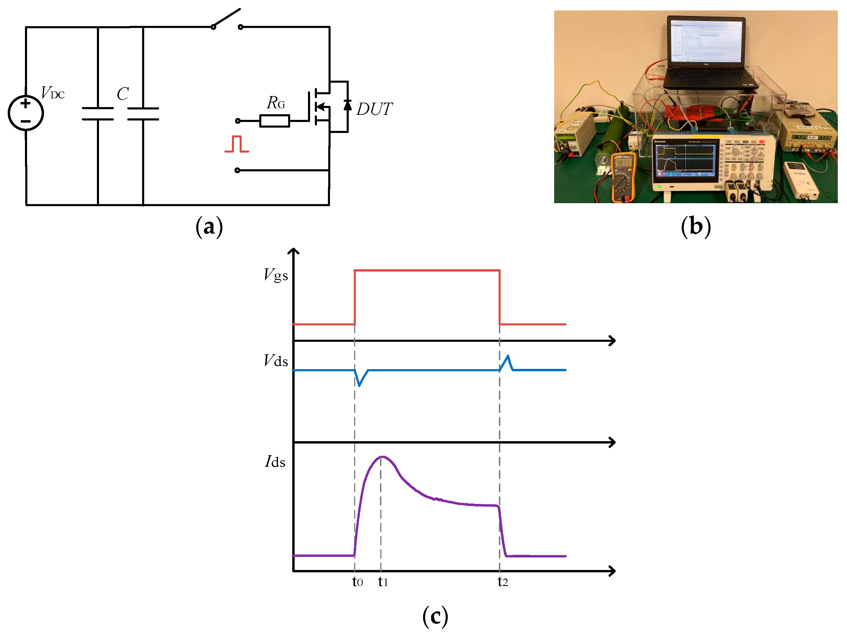
The studied SC characteristics were needed for characterization by a SC test platform. The SC characteristics test platform is shown in Figure 2. Figure 2a shows the schematic of SC test circuit. Figure 2b is the picture of the SC test platform. Figure 2c is the theoretical waveforms of SC.

3. Experimental Results

3.1. Measured Threshold Voltage after Irradiation

The measured threshold voltages (VTH) for the planar and trench SiC MOSFET at different dose levels are shown in Figure 3. The VTH decreases with dose for the planar and trench SiC MOSFET but with different rates of degradation. For the planar SiC MOSFET, the VTH degraded only about −1 V as the dose accumulated to 600 krad(Si). However, for the trench SiC MOSFET, the VTH shifts of approximately −2.5 V and −4.5 V for cool trench and double trench with dose accumulated to 150 krad(Si), respectively.

3.2. Measured SC Characteristics of Planar SiC MOSFET after Irradiation

Figure 4 shows the measured typical SC waveforms of the planar SiC MOSFET with a DC voltage as high as 600 V, which corresponds to 50% of the rated breakdown voltage. From Figure 4, it can be seen that, at the SC time reaches about 5.5 µs, the gate voltage drops rapidly to gate turn-off voltage. At this time, the drain current rapidly drops, but the device is not completely turned off, and the drain current slowly drops from about 28 A. However, as the SC time reaches about 8.2 µs, the gate voltage suddenly increases, and the device encounters a gate source failure. By testing the SC waveforms of the twelve planar SiC MOSFET samples, these devices’ SC failures before and after irradiation are all gate source failures, and the measured equivalent resistance of the gate source is several Ω to thousands of Ω.
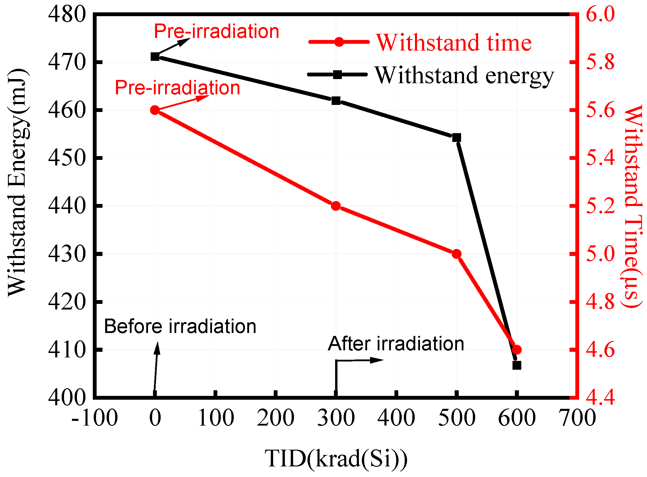
The SCWE and SCWT of the planar SiC MOSFET can be calculated by the SC waveforms of Figure 4, as shown in Figure 5. Figure 5 shows the SCWE and SCWT of the planar SiC MOSFET before and after irradiation. From Figure 5, it can be seen that, as the dose is accumulated to 300 krad(Si), SCWE and SCWT decrease to about 462 mJ and 5.2 µs from rated SCWE 471 mJ and rated SCWT 5.6 µs for fresh devices, respectively. The reduction rates of SCWE and SCWT are 1.9% and 7.1%, respectively. However, as the dose accumulates to 600 krad(Si), SCWE and SCWT decrease sharply to about 406 mJ and 4.6 µs, respectively. Their reduction rates are 13.8% and 17.9%, respectively. By comparing the degradation rates of SCWE and SCET at lower doses (TID = 300 krad(Si)) and higher doses (TID = 600 krad(Si)), we can know that the SC characteristics of planar SiC MOSFET are less affected by lower TID. For the abrupt reduction in SCWT at TID = 600 krad(Si), we guess that higher doses caused some defects inside the device.

3.3. Measured SC Characteristics of Trench SiC MOSFET after Irradiation

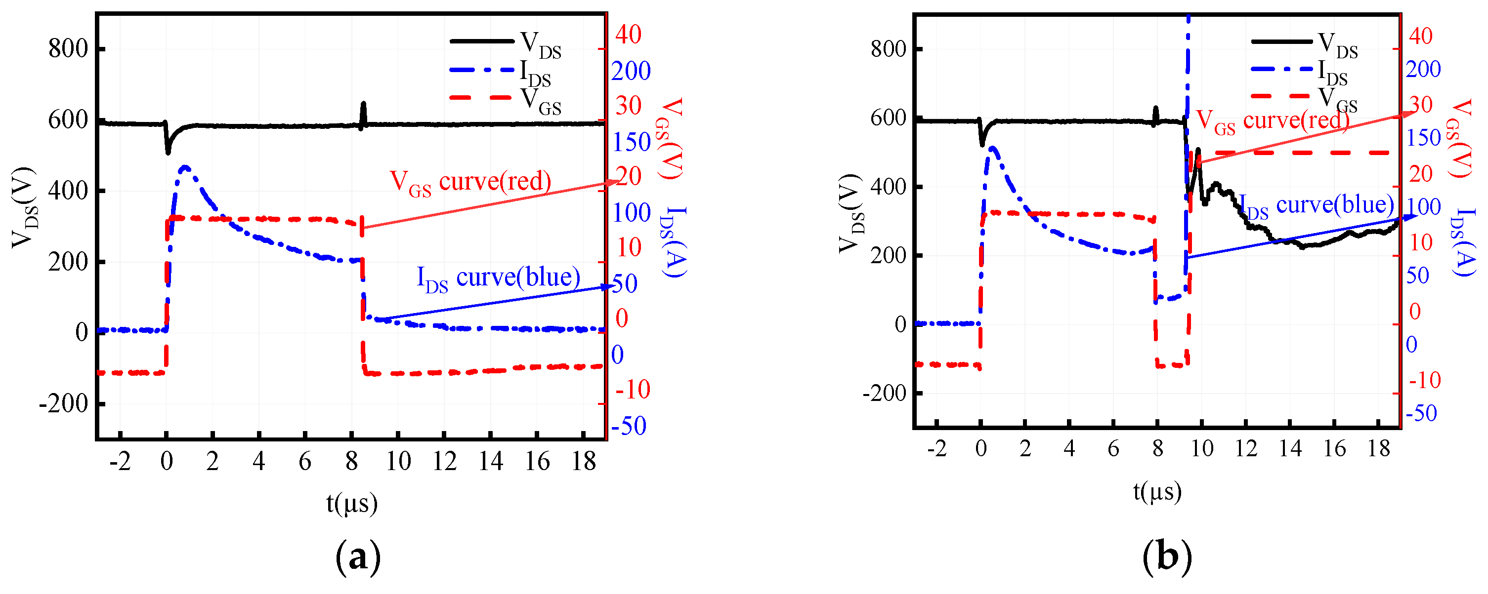
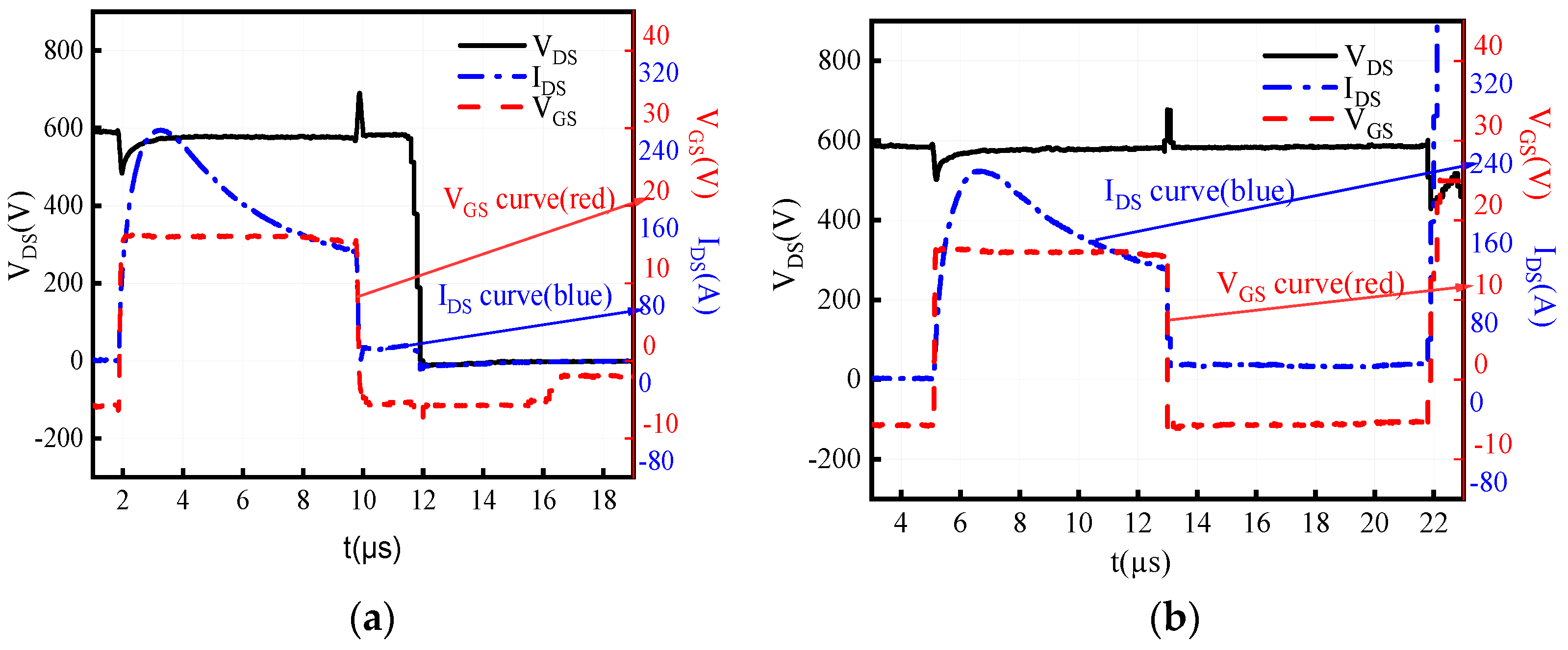
Figure 6 and Figure 7 are the typical SC waveforms of the cool trench and double trench SiC MOSFET with a DC voltage as high as 600 V, respectively. From Figure 6a and Figure 7a, we can see that the drain current of the cool trench and double trench SiC MOSFET drops slowly, while the gate voltage is turned off and then suddenly increases, and the devices encounter gate source failure. Figure 6b and Figure 7b show that the drain current of cool trench and double trench SiC MOSFET drops slowly, while the gate voltage is turned off and then the drain current and the gate voltage suddenly increase, and the devices encounter thermal runaway failure.
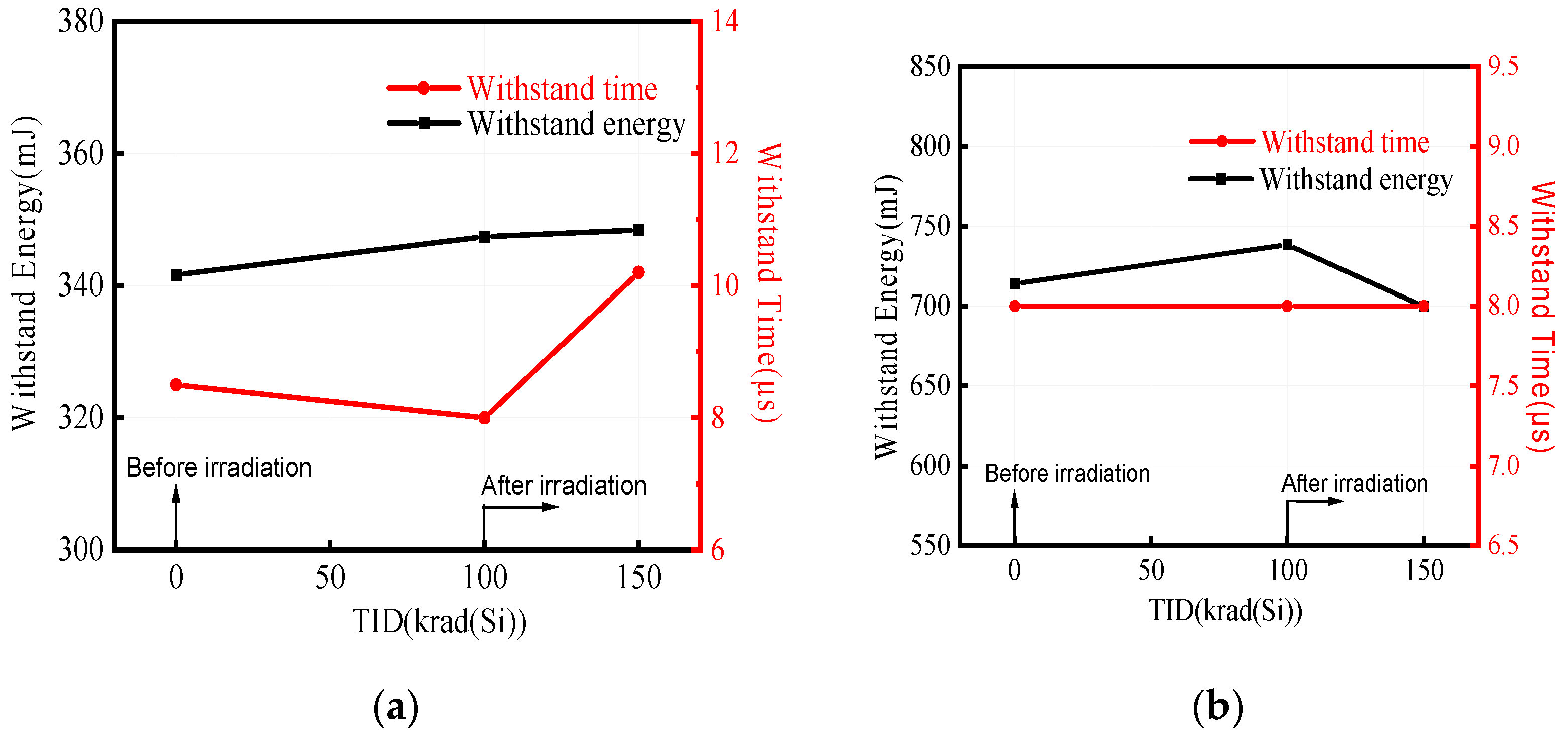
The SCWE and SCWT of the cool and double trench SiC MOSFET can be calculated by the SC waveforms of Figure 6 and Figure 7, as shown in Figure 8. Figure 8a,b shows the SCWE and SCWT of the cool and double trench SiC MOSFET before and after irradiation, respectively. From Figure 8a, it can be seen that, as the dose accumulated to 150 krad(Si), the SCWE and SCWT of the cool trench SiC MOSFET are improved, but these variations are very small. In addition, Figure 8b shows that, as the dose accumulated to 150 krad(Si), the SCWE and SCWT of the double trench SiC MOSFET did not change.

4. Analysis and Simulations

TID caused oxide-trapped charges and interface charges in the gate oxide (GOX) [15]. In contrast to the interface charges, TID caused substantial oxide-trapped charges in GOX. The trapped positive charge is the main cause of the threshold voltage shifting negatively. The radiation-induced trapped charges will influence the robustness of the device, and then affect the SC withstand. For example, the SCWT of the device decreases after irradiation, and the lattice temperature of the device after irradiation is significantly higher than that of the device before irradiation under the same SCWT conditions. Based on the above analysis, the reason for the SCWE and SCWT rapidly decreasing during higher dose levels is perhaps that the device works in a radiation environment for a long time, and the radiation-induced trapped charges will produce serious defects inside the device. In this analysis, although the VTH variation of the planar SiC MOSFET is much smaller than that of the trench SiC MOSFET under the higher dose levels, the SCWE and SCWT variation of the planar SiC MOSFET is larger.
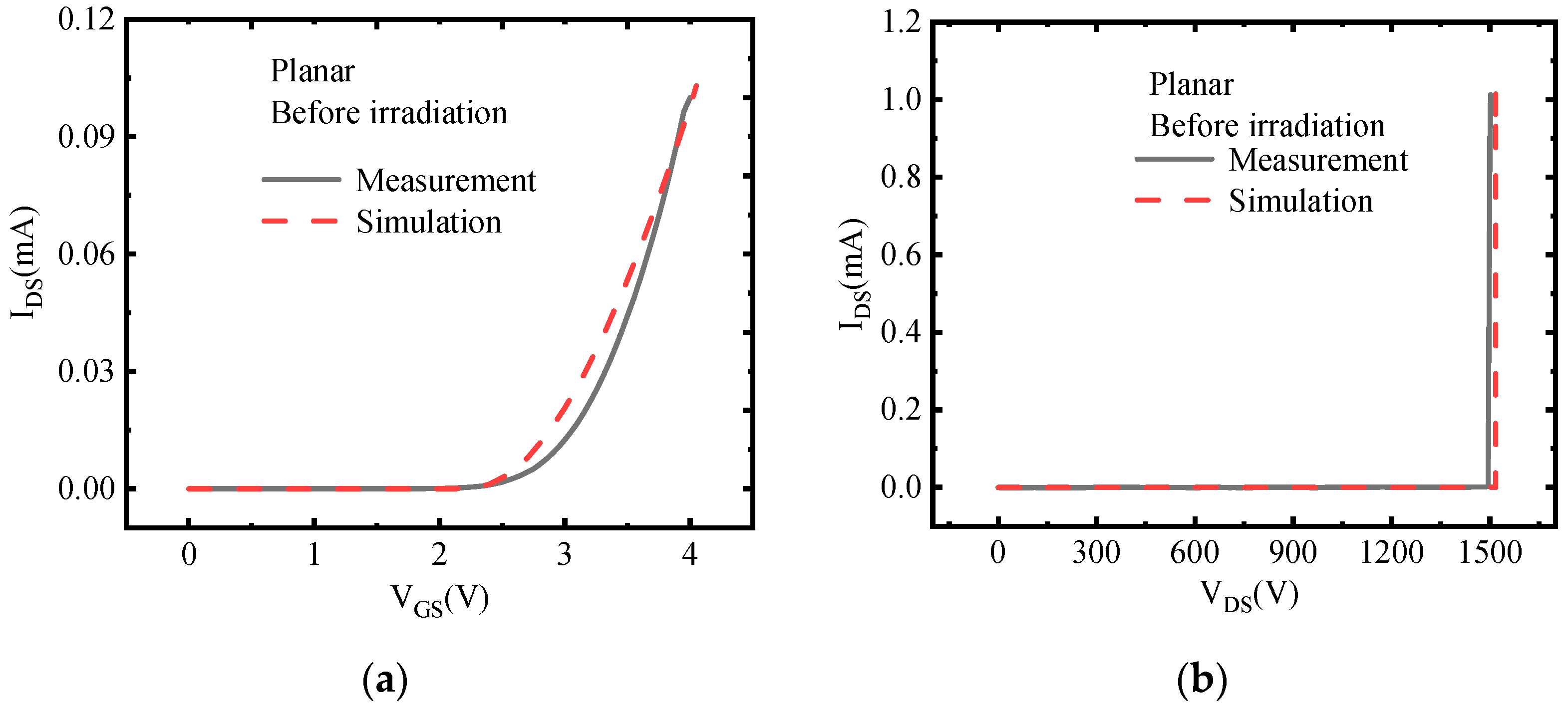
To further explore the mechanisms of the SCWE and SCWT variations before and after irradiation, 2D TCAD models are developed. We chose the SiC MOSFET of planar structure as an example for simulation studies. Standard SiC device physical models were used, including the Shockley–Read–Hall (SRH) recombination, mobility as a function of doping, and bandgap narrowing. The models were built based on the known structures (similar to those in Figure 1a) and parameters calibrated by fitting simulation results to measurement data for the fresh SiC MOSFET. Figure 9 shows the transfer characteristics (shown in Figure 9a) and breakdown characteristics (shown in Figure 9b) of the measured device and the simulation model. From Figure 9, it can be seen that the simulation results fit relatively well with the test results. To imitate the TID effect, charges are placed inside the GOX, 5 nm from the SiC-SiO2.
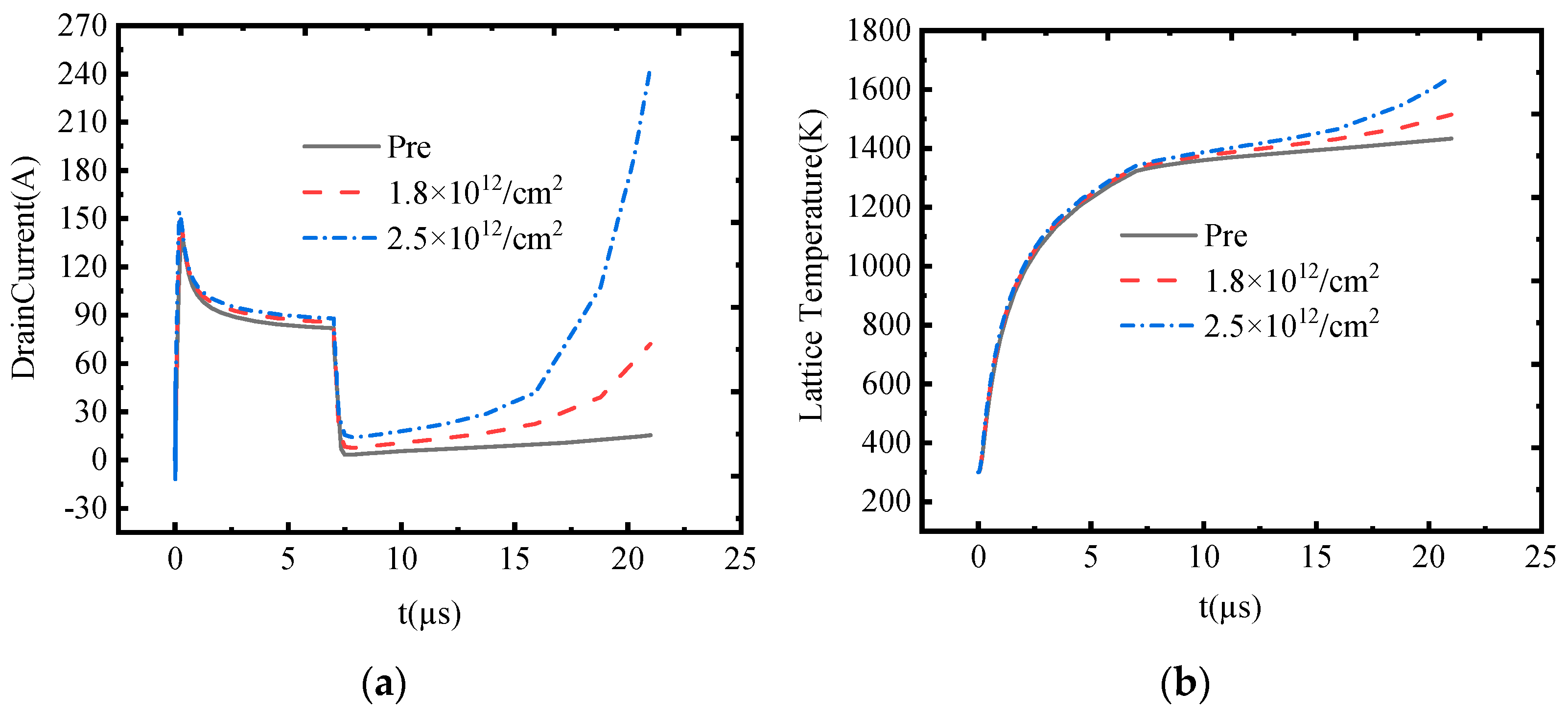
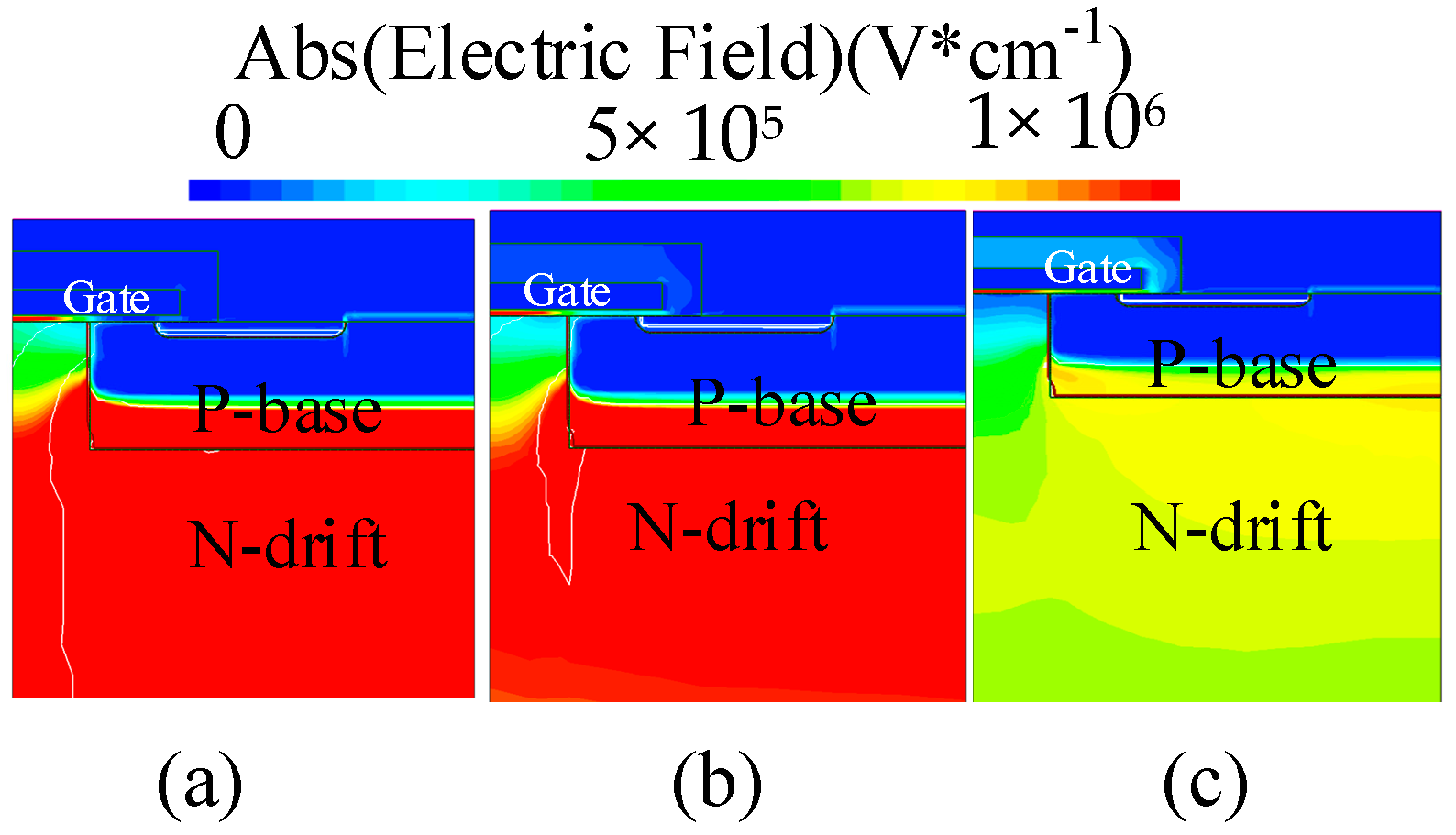
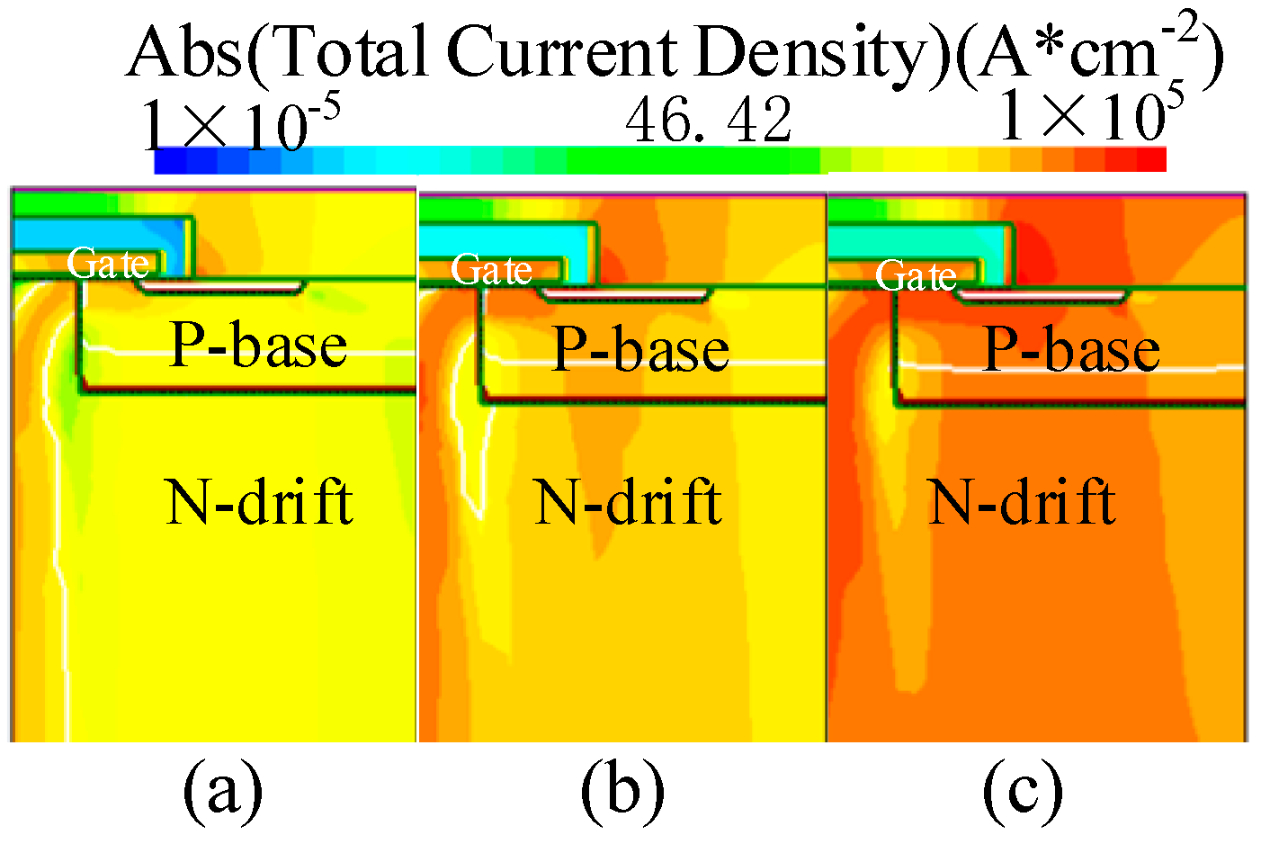
Figure 10a,b shows the simulation results of drain current and maximum lattice temperature for a fresh model and an irradiation model, respectively. From Figure 10a, we can see that the device failure at short-circuit time (tsc) is equal to about 7 µs after irradiation, while the device does not fail at tsc = 7 µs before irradiation. And, as the accumulated dose increases, the device failure is more serious. Figure 10b shows the lattice temperature of the device during SC states before and after irradiation. For the increase in the device lattice temperature, we speculate that this is due to the trapped charges in the GOX by the TID, which leads to the degradation of the VTH (as shown in Figure 3) of the device and generates damage inside the device. When the devices experience a SC, the damage caused by the TID inside the devices become more severe, resulting in an increase in the lattice temperature of the devices. The lattice temperature of the device increases continuously as the dose accumulates after tsc = 7 µs, as shown in Figure 11. Figure 11a–c shows the lattice temperature distribution of the device with tsc = 20 µs before and after irradiation, respectively. From Figure 11, it can be seen that the lattice temperature of the device is the highest at higher dose levels. A higher temperature will cause the device to heat up, causing the device to fail. When the device fails after a SC process, the physical phenomenon of the device after the failure shows that the electric field distribution around the drifting area and p-base decreases, as shown in Figure 12. In addition, the impact ionization distribution in these regions is also reduced, as shown in Figure 13. However, the total current density increases in these regions, as shown in Figure 14.

5. Conclusions

This paper experimentally measured the SCWE and SCWT variations for 1200 V commercial planar and trench SiC MOSFET power devices induced by TID. The SCWE and SCWT variations of planar and trench SiC MOSFET power devices behave differently before and after irradiation. Compared with the SCWE and SCWT variations of the planar and trench, the SCWE and SCWT of the planar changes greatly before and after irradiation, while the SCWE and SCWT of the trench are almost unchanged. These behaviors indicate that the SCWE and SCWT of different structural devices are greatly affected by the dose level. The higher dose level will make the SCWE and SCWT of these devices change greatly. The SCWE and SCWT variations of the planar SiC MOSFET can be attributed to radiation-induced charges in the GOX. These results provide some insights for the SiC MOSFET to be used in space radiation environments.

Author Contributions

Conceptualization, L.S.; methodology, S.-W.L.; software, X.-Y.F.; validation, T.-D.L. and L.W.; formal analysis, L.S.; investigation, L.S. and Y.-Y.L.; resources, J.W.; data curation, Z.-Y.W.; writing—original draft preparation, L.S.; writing—review and editing, Y.-F.Z.; visualization, Z.-Y.W.; supervision, H.-L.L.; project administration, Y.-F.Z.; funding acquisition, L.S. All authors have read and agreed to the published version of the manuscript.

Funding

This work was supported, in part, by the National Natural Science Foundation of China under Grant 62204019 and 52207199, and in part, by the Science and Technology Innovation Program of Hunan Province under Grant 2021RC2044.

Data Availability Statement

Not applicable.

Conflicts of Interest

The authors declare no conflict of interest.

References

  1. Lauenstein, J.-M.; Casey, M.C.; Ladbury, R.L.; Kim, H.S.; Phan, A.M.; Topper, A.D. Space Radiation Effects on SiC Power Device Reliability. In Proceedings of the International Reliability Physics Symposium IEEE, Monterey, CA, USA, 21–25 March 2021; IEEE: Piscataway, NJ, USA, 2021. [Google Scholar]
  2. Na, J.; Kim, K. A Novel 4H-SiC Double Trench MOSFET with Built-In MOS Channel Diode for Improved Switching Performance. Electronics 2023, 12, 92. [Google Scholar] [CrossRef]
  3. Sun, Y.; Wan, X.; Liu, Z.; Jin, H.; Yan, J.; Li, X.; Shi, Y. Investigation of total ionizing dose effects in 4H–SiC power MOSFET under gamma ray radiation. Radiat. Phys. Chem. 2022, 197, 110219. [Google Scholar] [CrossRef]
  4. Sun, J.; Wei, J.; Zheng, Z.; Wang, Y.; Chen, K.J. Short circuit capacity and short circuit induced VTH instability of a 1.2 kV SiC power MOSFET. IEEE J. Emerg. Sel. Top. Power Electron. 2019, 7, 1539–1546. [Google Scholar] [CrossRef]
  5. Luo, Z.; Chen, T.; Cressler, J.D.; Sheridan, D.C.; Williams, J.R.; Reed, R.A.; Marshall, P.W. Impact of proton irradiation on the static and dynamic characteristics of high-voltage 4H-SiC JBS switching diodes. IEEE Trans. Nucl. Sci. 2003, 50, 1821–1826. [Google Scholar]
  6. Pappis, D.; de Menezes, L.; Zacharias, P. Comparison of the Short Circuit Capability of Planar and Trench SiC MOSFETs. In Proceedings of the PCIM Europe 2017; International Exhibition and Conference for Power Electronics, Intelligent Motion, Renewable Energy and Energy Management, Nuremberg, Germany, 16–18 May 2017; Volume 2017, pp. 854–862. [Google Scholar]
  7. Okawa, M.; Aiba, R.; Kanamori, T.; Yano, H.; Iwamuro, N.; Harada, S. Experimental and numerical investigations of short-circuit failure mechanisms for state-of-the-art 1.2 kV SiC trench MOSFETs. In Proceedings of the 2019 31st International Symposium on Power Semiconductor Devices and ICs (ISPSD), Shanghai, China, 19–23 May 2019; pp. 167–170. [Google Scholar]
  8. Lin, C.; Wu, J.; Xu, H.; Ren, N.; Guo, Q.; Sheng, K. Comparison and Analysis of Short Circuit Performance of 1200 V SiC MOSFETs. In Proceedings of the 2020 17th China International Forum on Solid State Lighting & 2020 International Forum on Wide Bandgap Semiconductors China (SSLChina: IFWS), Shenzhen, China, 23–25 November 2020; pp. 81–84. [Google Scholar]
  9. Gonzalez, J.O.; Deb, A.; Bashar, E.; Agbo, S.; Jahdi, S.; Alatise, O. Benchmarking the robustness of Si and SiC MOSFETs: Unclamped inductive switching and short-circuit performance. Microelectron. Reliab. 2022, 138, 114719. [Google Scholar] [CrossRef]
  10. Bashar, E.; Agbo, N.; Wu, R.; Mendy, S.; Jahdi, S.; Jennings, M.; Withey, A.; Evans, S.; Davies, G.; Demitrova, J.; et al. A Review of Short Circuit Performance in 650 V Power Devices: SiC MOSFETs, Silicon Super-junction MOSFETs, SiC Cascode JFETs, Silicon MOSFETs and Silicon IGBTs. In Proceedings of the International Exhibition and Conference for Power Electronics, Intelligent Motion, Renewable Energy and Energy Management, Nuremberg, Germany, 10–12 May 2022; pp. 1–8. [Google Scholar]
  11. Kakarla, B.; Tsibizov, A.; Stark, R.; Badstübner, I.K.; Grossner, U. Short circuit robustness and carrier lifetime in silicon carbide MOSFETs. In Proceedings of the 32nd International Symposium on Power Semiconductor Devices and ICs (ISPSD), Vienna, Austria, 13–18 September 2020; pp. 234–237. [Google Scholar]
  12. Hazdra, P.; Popelka, S. Displacement damage and total ionization dose effects on 4H-SiC power devices. IET Power Electron 2019, 12, 3910–3918. [Google Scholar] [CrossRef]
  13. Hu, D.; Zhang, J.; Jia, Y.; Wu, Y.; Peng, L.; Tang, Y. Impact of different gate biases on irradiation and annealing responses of SiC MOSFETs. IEEE Trans. Electron Devices 2018, 65, 3719–3724. [Google Scholar] [CrossRef]
  14. Akturk, A.; McGarrity, J.M.; Potbhare, S.; Goldsman, N. Radiation Effects in Commercial 1200 V 24 A Silicon Carbide Power MOSFETs. IEEE Trans. Nucl. Sci. 2012, 59, 3258–3264. [Google Scholar] [CrossRef]
  15. Schwank, J.R.; Shaneyfelt, M.R.; Fleetwood, D.M.; Felix, J.A.; Dodd, P.E.; Paillet, P.; Ferlet-Cavrois, V. Radiation effects in MOS oxides. IEEE Trans. Nucl. Sci. 2008, 55, 1833–1853. [Google Scholar] [CrossRef]
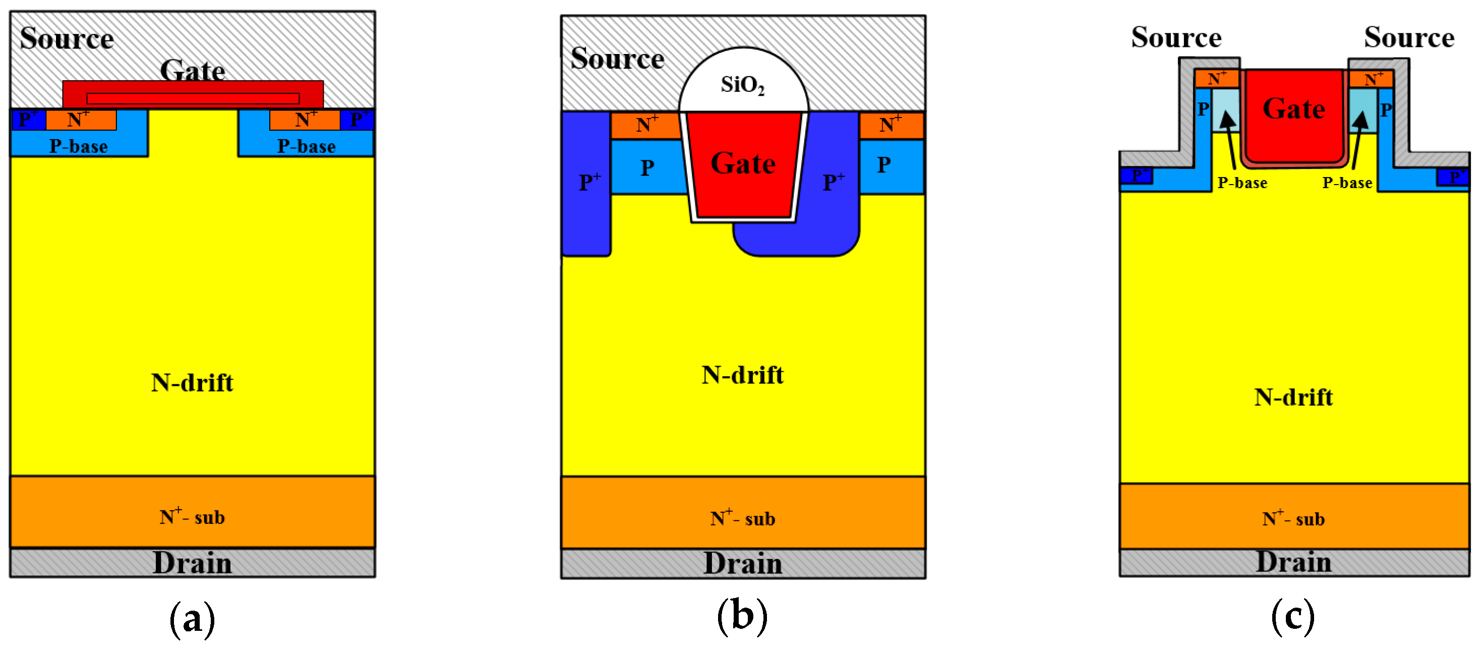
Figure 1. Schematic cross-sectional view of (a) planar structure, (b) trench structure and (c) double trench structure of SiC MOSFET power devices.
Electronics 12 02891 g001
Figure 2. SC test platform. (a) The schematic of SC test circuit, (b) a picture of the SC test platform and (c) SC theoretical waveforms.
Electronics 12 02891 g002
Figure 3. Measured VTH variations of planar and trench SiC MOSFET with different accumulated doses.
Electronics 12 02891 g003
Figure 4. Measured SC waveforms of planar SiC MOSFET.
Electronics 12 02891 g004
Figure 5. Calculated SCWE and SCWT of planar SiC MOSFET before and after irradiation.
Electronics 12 02891 g005
Figure 6. Measured SC waveforms of trench SiC MOSFET. (a) Gate-source failure and (b) thermal runaway failure.
Electronics 12 02891 g006
Figure 7. Measured SC waveforms of double trench SiC MOSFET. (a) Gate-source failure and (b) thermal failure.
Electronics 12 02891 g007
Figure 8. Calculated SCWE and SCWT of SiC MOSFET before and after irradiation. (a) Cool trench SiC MOSFET and (b) double trench SiC MOSFET.
Electronics 12 02891 g008
Figure 9. Simulation and measured non-irradiated (a) threshold characteristics and (b) breakdown characteristics curves for SiC MOSFET power devices with planar structure.
Electronics 12 02891 g009
Figure 10. Simulated (a) drain current and (b) maximum lattice temperature of SiC MOSFET during SC test before and after irradiation with Not_GOX = 1.8 × 10¹²/cm2 and Not_GOX = 2.5 × 10¹²/cm2.
Electronics 12 02891 g010
Figure 11. Simulated lattice temperature distribution of the SiC MOSFET with tsc equal to 20 µs (a) before irradiation and after irradiation with (b) Not_GOX = 1.8 × 10¹²/cm2 and (c) Not_GOX = 2.5 × 10¹²/cm2.
Electronics 12 02891 g011
Figure 12. Simulation results of electric field distribution under the short-circuit state of tsc equal to 20 µs (a) before irradiation and after irradiation with (b) Not_GOX = 1.8 × 10¹²/cm2 and (c) Not_GOX = 2.5 × 10¹²/cm2.
Electronics 12 02891 g012
Figure 13. Simulated impact ionization distribution of the SiC MOSFET with tsc equal to 20 µs (a) before irradiation and after irradiation with (b) Not_GOX = 1.8 × 10¹²/cm2 and (c) Not_GOX = 2.5 × 10¹²/cm2.
Electronics 12 02891 g013
Figure 14. Simulated total current density distribution of the SiC MOSFET with tsc equal to 20 µs (a) before irradiation and after irradiation with (b) Not_GOX = 1.8 × 10¹²/cm2 and (c) Not_GOX = 2.5 × 10¹²/cm2.
Electronics 12 02891 g014
Disclaimer/Publisher’s Note: The statements, opinions and data contained in all publications are solely those of the individual author(s) and contributor(s) and not of MDPI and/or the editor(s). MDPI and/or the editor(s) disclaim responsibility for any injury to people or property resulting from any ideas, methods, instructions or products referred to in the content.