Article

A H-Bridge-Multiplexing-Based Novel Power Electronic Transformer

National Engineering Research Center for Rare Earth Permanent Magnet Machine, Shenyang University of Technology, Shenyang 110870, China
*
Author to whom correspondence should be addressed.
Electronics 2024, 13(1), 22; https://doi.org/10.3390/electronics13010022
Submission received: 6 November 2023 / Revised: 17 December 2023 / Accepted: 18 December 2023 / Published: 20 December 2023

Abstract

:
Cascaded H-bridge power electronic transformers (CHB-PET) play a pivotal role in distribution grids and their efficient operation. The input series and output parallel (ISOP) configurations result in a huge number of power switching devices, high-frequency transformers (HFT), and capacitors in high-voltage, high-capacity CHB-PET, leading to the need for high hardware costs and huge-sized CHB-PET, which further poses a significant challenge to the engineering feasibility and marketability of the CHB-PET. To address these issues, a CHB-PET topology is proposed in this paper. The novel topology exploits the concept of multi-frequency modulation to achieve power decoupling and power unit multiplexing through reasonable LC resonant frequency selection, which optimizes the ISOP structure and ultimately reduces the hardware cost and size of the CHB-PET. In this study, the effectiveness of reducing the number of power switching devices and HFT is firstly analyzed, and after describing its working principle, the control strategy of each power conversion link of PET is discussed before the correctness and effectiveness of the CHB-PET topology and control strategy proposed in this paper are verified via simulation.

1. Introduction

In the pursuit of “carbon neutrality”, there is a global expansion in the scale and utilization of renewable energy sources such as solar energy and wind energy. As the development and utilization of new energy forms emerge, the deployment of smart grids [1,2,3] has emerged as a powerful strategy to achieve “carbon neutrality.” Within the framework of the smart grid, the power electronic transformer assumes a pivotal role in facilitating the bidirectional flow of electrical energy and providing interfaces for various forms of new energy [4,5]. Consequently, extensive research is being conducted to explore the topology and control strategies of power electronic transformers, owing to their significant implications.
Presently, in the design of power electronic transformers (PET), various universities and institutes [6,7,8,9,10,11,12] have widely adopted the topology depicted in Figure 1. When a PET is employed in distribution networks, the H-bridge can be cascaded to enhance the voltage level of the rectifier when the power semiconductor device’s voltage capability is limited. This cascaded structure, known as Cascade H-bridge PET (CHB-PET), incorporates a number of high-frequency transformers (HFT) aligned with the cascaded units. Among the multiple cascaded cells, an input series output parallel (ISOP) configuration is adopted. Each individual cascaded cell, referred to as a submodule, consists of an AC/DC converter connected in series with a dual active bridge DC/DC converter. While this structure improves the performance of the PET, it necessitates the use of a larger number of power switching devices and HFTs. Consequently, this increased hardware demand directly results in higher costs and larger volumes, which hampers the engineering implementation and marketability of PETs [13,14,15].
One of the developmental directions of CHB-PET focuses on improving the power density of the entire PET system by reducing the number of power conversion stages, power switching devices, and HFTs [16,17,18,19,20]. In addressing the limitations of CHB-PET in distribution networks, the topology can be enhanced by multiplexing the bridge arm of the H-bridge configuration. In a previous study [16], a high-power-density PET suitable for medium and high voltage distribution networks was designed. The frequency selection functionality of series resonance was employed to effectively reduce the usage of power devices and HFTs. Furthermore, in another study [17], the concept of mixing modulation was introduced, leading to the design of two novel cascaded PET topologies. Additionally, in a different research work [18], a full-bridge compensation module was introduced to devise a single-phase cascaded PET topology.
H-bridge multiplexing is one idea for developing a new CHB-PET, and one study [21] designed a PET based on time-sharing multiplexing by analogy with the time-sharing multiplexing of channels through communication collars. In this paper, under the same idea, a new three-phase CHB-PET topology is proposed, which is shown in Figure 2. Compared with the topology in [21], the novel structure designed in this paper adopts the idea of frequency division multiplexing and uses a passive network for demodulation, which reduces the difficulty of control.
The novel topology of Figure 2 adopts the full bridge as the submodule, enabling the input-side converter to transmit both power frequency and high-frequency power by multiplexing the H-bridge arm. In comparison to the traditional three-stage PET [22,23,24,25,26,27,28,29,30], this novel topology retains the DC bus port while eliminating the H-bridge on the input side of the dual active bridge (DAB) converter. Compared with the ISOP structure, the number of power devices and HFTs is reduced, effectively lowering the hardware cost and overall machine volume, while simultaneously improving the power density and compactness of the PET.
The subsequent section provides a detailed description of this novel topology and elucidates its operational principles. The control structure design and main circuit parameter considerations are discussed extensively in Section 3 and Section 4, respectively. Finally, according to the topologies shown in Figure 1 and Figure 2, the corresponding simulation models are built in PLECS, respectively, and an in-depth simulation analysis is carried out via comparison.
By comprehensively evaluating the performance of the proposed topology and verifying its effectiveness through simulation analysis, this study contributes to the advancement of CHB-PET technology. The results obtained from this research will facilitate the deployment of more efficient and compact power electronic transformers, fostering their wider adoption in practical applications.

2. Proposing a Novel Topology

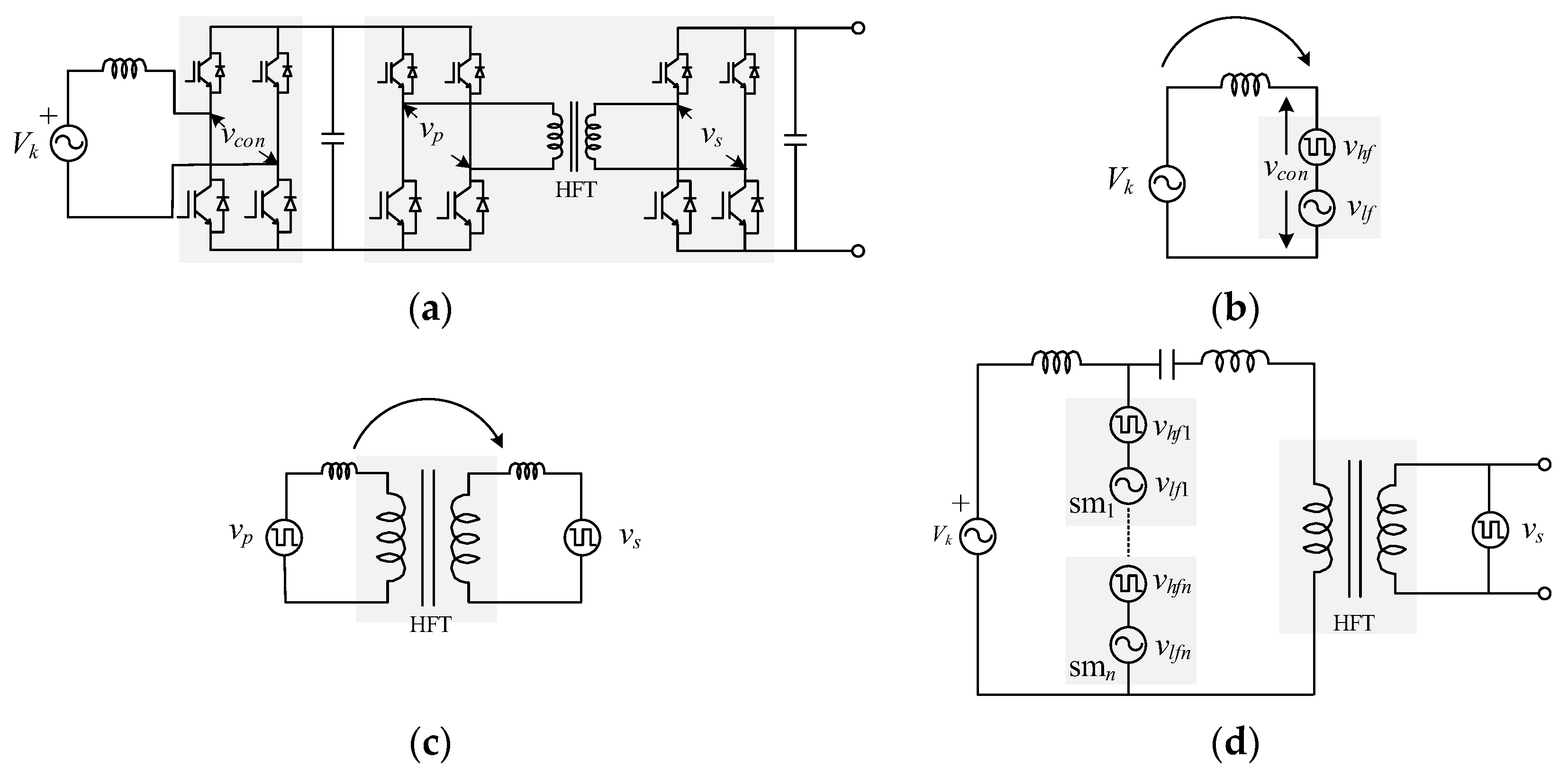
2.1. Description of Topology

The proposed novel topology, depicted in Figure 2, showcases the isolation of the power grid and the load through the utilization of high-frequency transformers. In phase A, the primary side of the HFT comprises a cascade of n full-bridge modules, while the secondary side consists of a single full-bridge configuration (S5–S8). The filter inductor Lsa acts as a low-pass filter, effectively attenuating high-frequency currents and providing reactive connection. The resonant capacitor Cr and resonant inductor Lr form a band-pass filter, which effectively suppresses power frequency currents while offering a low-impedance pathway for high-frequency currents. The structure of phases B and C mirrors that of phase A. Upon parallel connection of the DC bus, the full bridge configuration (S9–S14) is employed for AC output inversion. For the sake of convenience, the circuit preceding the DC bus is collectively referred to as the front circuit, whereas the inverter and load form the back circuit. Considering the positioning of the high-frequency transformer, the front circuit is further categorized into the primary side circuit and the secondary side circuit. By establishing a clear and well-defined circuit distinction between the front and back circuits and the primary and secondary side circuits, the proposed topology facilitates a comprehensive understanding and analysis of the system’s operation and performance. The subsequent sections will delve into a detailed discussion of each circuit’s control strategy, ensuring a holistic exploration of the proposed topology’s effectiveness and functionality.

2.2. Topology Evolution and Working Principle

The proposed topology in this study is a conceptual integration of the PWM voltage source rectifier (VSR), DAB DC-DC converter, and PWM voltage source inverter (VSI). Figure 3a shows the internal structure of the cascade unit in Figure 1, including the AC/DC conversion and DAB links. In the AC/DC link, when PWM modulation is used, the H-bridge arm voltage is a superposition of multiple frequency voltages when two and more frequency signal waves are used as modulating waves. As shown in Figure 3b, the superposition of signal waves with frequencies of flf and fhf can drive the H-bridge to output voltages of two frequencies, vlf and vhf. In the DAB link, the equivalent circuits on both sides of the HFT are shown in Figure 3c, which transform the high-frequency voltage vp into vk.
The combination of VSR and DAB is the key aspect of the novel topology, as depicted in Figure 3d. According to the previous analysis, the bridge arm of the AC/DC link can be connected to the mains via the low-pass filter Lsa and at the same time to the HFT via the LC resonant circuit. The joint action of the low-pass filter and the LC resonant circuit allows the AC voltage components vlf and vhf to be transmitted to the power supply vs. and the HFT, respectively. Zero current switching can be achieved when the frequency of vhf matches the resonant frequency of the LC circuit and the switching frequency of the full-bridge (S5–S8). At this point, the AC square wave nature of vhf aids in reducing losses and improving the efficiency of PET energy conversion. Ultimately, the topology accomplishes power decoupling and enables the reuse of power units.
By establishing this novel topology, this study significantly advances the state of the art in power electronic transformer design and offers enhanced power decoupling capabilities and power unit reuse. The subsequent sections will provide in-depth analyses of the proposed topology’s performance, control strategies, and efficiency evaluation to validate its effectiveness in practical applications.

2.3. Mathematical Models and Switching Signals

Regarding the three-phase PET topology depicted in Figure 2, the rear circuit is associated with a resistive load connected to the low-voltage DC bus. Since the control strategy of the front circuit remains unaffected, the focus of this paper is solely on the analysis of the front circuit. Recognizing that the correlation analysis of three-phase inverters has reached a mature stage, this study exclusively examines the front circuit, which can be represented by its equivalent circuit illustrated in Figure 4.
In this, the AC side inductance Lsk (k = a,b,c) includes the inductance of the external reactor and the internal inductance of the power supply; the resistance rsk includes the resistance of the external reactor and the internal resistance of the power supply; inductance Lrk comprises an external reactor inductance and a high-frequency transformer leakage inductance; capacitor Crk and inductance Lrk form the LC filter.
To facilitate analysis, it is assumed that the parameters of each phase inductor, LC filter, high-frequency transformer, and submodule are identical. Additionally, the subharmonic component of the switching frequency is neglected.
Following a comprehensive examination of the equivalent circuit depicted in Figure 4, equations based on KVL can be derived as follows:
L s d i k d t = v k r s i k v con , k v NO ,
where voltage vk is the three-phase power grid voltage on the AC side and current ik is the input current on the AC side. vcon,k is the mid-point voltage of the bridge arm, which can be decomposed into the components vk,lf and vk,hf whose frequencies are 50 Hz and fh, respectively, and satisfying vcon,k = vk,lf + vk,hf.
Equation (1) can be expressed as follows:
L s d i k d t = v k r s i k v k , lf v k , hf v NO ,
Then, after a simple operation, the following equation can be obtained:
L s d d t i a i b + r s i a i b = i a i b v a , lf v b , lf ( v a , hf v b , hf ) ,
where the voltage quantities va, vb, va,lf, and vb,lf are all of industrial frequency. When va,hf = vb,hf, there are only industrial frequency components in ia and ib.
Similarly, when va,hf = vc,hf, there are only industrial frequency components in ia and ic. Therefore, if the three-phase grid current is not required to contain high-frequency harmonics, it is necessary to satisfy the equation va,hf = vb,hf = vc,hf, and for ease of representation, the voltage is noted as vhf.
For the CHB in Figure 2, the total bridge arm current iarm,k can be decomposed into the components ik and ipk whose frequencies are 50 Hz and fh, respectively. Since the LC filter resonant frequency is fh, then the voltages of the filter should be vk,lf, and the voltage at the primary side of the HFT is vk,hf. Meanwhile, the current at the primary side of the HFT is ipk, and ipk is in phase with vk,hf. The previous analysis found that the voltage components of each phase should meet va,hf = vb,hf = vc,hf. Since the same load is used in each phase, the transformer primary current should meet ipa = ipb = ipc, and for ease of representation, the current is recorded as ip.
According to Equation (2), the following equations can be written as follows:
L s d d t k = a , b , c i k + r s k = a , b , c i k = k = a , b , c v k k = a , b , c v k , lf k = a , b , c v k , hf 3 v NO ,
The expansion module depicted in Figure 4 adopts a PWM control strategy. When a power frequency sinusoidal signal wave is employed as the modulated waveform, the condition va,lf + vb,lf + vc,lf = 0 is satisfied. Additionally, owing to the three-phase symmetry of the AC power supply on the input side, it satisfies, va + vb + vc = 0, ia + ib + ic = 0. The following relationship can be derived:
v NO = 1 3 k = a , b , c v k , hf ,
Equation (1) can be resolved:
L s d i k d t = v k r s i k v k , lf ,
If the voltage across a single H-bridge shunt capacitor is vsm, the AC side of a single H-bridge can exhibit three voltage states when the H-bridge is modulated with unipolar modulation: “vsm”, “−vsm”, and “0”. The A-phase circuit is analyzed below: the high-voltage side cascades n sub-modules as a whole, numbering the switches within the nth sub-module as Sn,1, Sn,2, Sn,3, and Sn,4. Assuming that the circuit parameters of the n sub-modules are the same, when Sn,1 and Sn,4 are switched on, the ac side voltage vcon,a is given by vcon,a = n vsm; when Sn,2 and Sn,3 are switched on, vcon,a = −n vsm; when either Sn,1 and Sn,3 or Sn,2 and Sn,4 are switched on, vcon,a = 0. To simplify the analysis, the switching function sk is introduced. When the switch is on, the device state is denoted as 1; otherwise it is denoted as 0. Thus, sk = Sn,1 − Sn,3 or sk = Sn,4 − Sn,2.
For the structure presented in Figure 2, the input-side cascade unit undergoes PWM modulation. The modulating waveforms with frequencies flf and fhf, respectively, are overlaid to create the new modulating waveform. As a result of the multi-frequency frequency modulation, the H-bridge bridge arm voltage is a coupling of two voltage components. The first component is the voltage vlf with a frequency of flf, and the corresponding switching function that generates this voltage is denoted as sk,lf. The other component is the voltage vhf at the frequency of fhf, and the corresponding switching function that generates this voltage is denoted as sk,hf. In simpler terms, it is possible to separate the switching function sk into sk,lf and sk,hf. To ensure the equality of the high-frequency voltage components across all phase bridge arm voltages, it is required that sa,hf = sb,hf = sc,hf = shf. The voltage of the AC side bridge arm and the current flowing through the submodule capacitor can be expressed as follows:
v k , lf = i = 1 n s k , lf v sm i , k = s k , lf n v sm v hf = i = 1 n s hf n v sm i , k = s hf n v sm i sm = s k i arm , k = ( s k , lf + s hf ) ( i k i p ) ,
where vsmi,k is the voltage across the i-th submodule capacitor in a k-phase cascade. When the hardware parameters of each submodule are the same, it satisfies vsmi,k = vsm.
Within a switching cycle Ts, the DC voltage vsm at the capacitor terminals experiences minimal variation and can be considered constant. The switching functions sk,lf can be represented by the duty ratio dk,lf. Consequently, the average model can be derived from Equation (6) as follows:
L s d i k d t = v k r s i k d k , lf n v sm ,
The AC-side variables are characterized by time-varying AC quantities, which poses challenges for subsequent controller design. To facilitate the design of the control system, the average mathematical model in the abc coordinate system is transformed into the dq coordinate system. This transformation allows for the conversion of all sinusoidal variables into relative DC variables. By applying the Park transformation to both sides of Equation (8), the average mathematical model is expressed in the rotating coordinate system of dq as follows:
L s d d t i d i q = V d V q r s ω g L s ω g L s r s i d i q n v sm d d , lf d q , lf ,
where Yd and Yq represent variables Y in the static coordinate system and corresponding variables in the dq coordinate system.
Within a switching cycle Ts, the average model of submodules can be obtained from Equation (6) as follows:
C sm d d t v sm = d k , lf i k + d hf i k d k , lf i p d hf i p ,
Equation (10) reveals that the current passing through the submodule capacitor encompasses both high-frequency square wave and power frequency sine components. Considering that the switching period Th is significantly smaller than Ts, the variables ik and dk,lf experience minimal changes within Th and can be treated as constants. Moreover, the mean values of variables ip and dhf within Th are determined to be zero. Consequently, the capacitance current of the submodule can be represented as follows:
C sm d d t v sm = 1 3 k = a , b , c d k , lf i k d hf i p ,
Since ip and dhf have the same frequency and phase, Equation (11) can be expressed as follows:
C sm d d t v sm = 1 3 k = a , b , c d k , lf i k 1 λ m i p ,
where m is the modulation ratio, which can be obtained by Equation (13). λ is the sinusoidal voltage amplitude output by the submodule, which can be obtained by Equation (14).
m = v a , lf , max + v hf , max n v sm , ref ,
λ = v a , lf , max v a , lf , max + v hf , max ,
Park transformation is applied to both sides of Equation (12), and the average mathematical model under the dq coordinate system can be written as follows:
C sm d d t v sm = 1 2 ( i d d d , lf + i q d q , lf ) 1 λ m i p ,
Assuming the turns ratio of the high-frequency transformer is denoted as kT, the secondary side voltage of the high-frequency transformer satisfies the relationship vsa = vsb = vsc = vh/kT, while the secondary side current is given by isa = isb = isc = kT ip.
Regarding the H-bridge configuration on the secondary side of the A-phase, the upper and lower switches of each bridge arm exhibit complementary on and off states, whereas the switches positioned diagonally are synchronized in their on and off states. When S5 and S8 are turned on, the AC side voltage corresponds to vsa = vdc. Conversely, when S6 and S7 are activated, vsa takes the value of −vdc. To simplify the analysis, we introduce the switch function sh, which assumes a value of 1 when the switch is on and 0 when it is off. Therefore, we can express sh as sh = S5–S7. Within a switching cycle Th, the switching function can be equivalently represented using the duty ratio, given by the following expression:
v hf = k T d h v dc C dc d d t v dc = k T d h i p v dc 3 R L ,
The switching function sh is in the same frequency and phase as the high-frequency square wave voltage vhf and the high-frequency sinusoidal current ip, giving the following:
C dc d d t v dc = k T i p v dc 3 R L ,
Figure 5 illustrates the average model of the preceding circuit stage in the dq coordinate system, which is derived based on Equations (9), (15) and (17).

3. Control Structure

Equation (9) presents the mathematical model in the dq coordinate system, revealing the interdependence between the d-axis and q-axis variables. This coupling hinders the controller design process. To address this issue, a feedforward decoupling control strategy for id and iq is introduced, enabling the compensation of vd,lf and vq,lf. By employing a PI regulator in the current control loop, the governing equation can be expressed as follows:
v d , lf * = k p 1 + k i 1 s i d * i d + ω L s i q + V d v q , lf * = k p 1 + k i 1 s i q * i q ω L s i d + V q ,
where kp1 and ki1 are proportional and integral adjustment gains of the current loop, respectively. id* and iq* are the current commands of axis d and axis q, respectively.
Equation (15) elucidates the mathematical model in the dq coordinate system. By setting the reactive current to zero, the system operates at a per-unit power factor, enabling the grid-side current to track the voltage without any static error. When employing a PI regulator for the voltage regulation, the governing equation can be expressed as follows:
i d * = k p 2 + k i 2 s v smref v sm i q * = 0 ,
where kp2 and ki2 are proportional and integral regulation gains of the submodule voltage loop, respectively. vsmref is the reference value of the capacitor voltage of the submodule.
By substituting Equations (18) and (19) into Equations (9) and (15), respectively, we can derive the system equation for the primary side circuit.
L s d d t i d + r s i d = k p 1 + k i 1 s i d * i d L s d d t i q + r s i q = k p 1 + k i 1 s i q * i q 2 C sm d d t v sm = k p 2 + k i 2 s v sm * v sm 1 λ m i p ,
When the output voltage regulator uses a PI regulator, the governing equation can be expressed as follows:
v hf , max * = k p 3 + k i 3 s v dcref v dc ,
where kp3 and ki3 are proportional and integral control gains of the output voltage loop, respectively. vdcref is the reference value of the output DC voltage.
The control block diagram of the three-phase CHB-PET can be constructed based on Equations (18)–(21). Figure 6 illustrates the control structure of the preceding circuit. The first control loop generates a sinusoidal AC signal wave uk,lf, operating as follows:
Equation (20) demonstrates the complete decoupling of active and reactive currents. Due to the small value of rsid, when the active current id is less than the reference current id*, Lsdid/dt > 0, resulting in a gradual increase in active current. Conversely, the active current gradually decreases. The principle of reactive current control is analogous. Both active and reactive power instruction currents are continuous flows. The given value of the active current is derived from the output of the voltage loop, while the corresponding value of the reactive current can be set as desired. The voltage loop employs a PI controller to regulate the average value of the DC capacitor voltage of the cascade submodule, which serves as the reference value to obtain the active current instruction value for the current loop. When the reactive current is set to zero, the system operates at unity power factor, enabling the current on the grid side to track the voltage without static deviation.
The second part of the control loop focuses on controlling the H-bridge to generate a square wave voltage with the same frequency and phase as the high-frequency voltage signal vhf. By utilizing a PI controller to adjust the output DC voltage vdc as a reference value, the reference value for the vhf peak is obtained. This leads to the generation of a bipolar square wave signal, which is superimposed with the sine wave uk,lf to form a new signal wave.
It should be noted that the cascade link consists of n H-bridge submodules. In this study, the CPS-PWM modulation method is employed, which sequentially shifts the triangular carrier of each power unit by 1/n carrier period. The shifted triangular carrier is then compared with the same signal wave to obtain the PWM control signal for each power unit. This modulation scheme enhances the high-frequency harmonic components in the output voltage spectrum and significantly reduces the size of the filter inductance. Since Lr and Cr form a series resonant circuit, the H-bridge switch tube can operate in the zero current switching state. The detailed design of the controller loop will be discussed in the following sections.

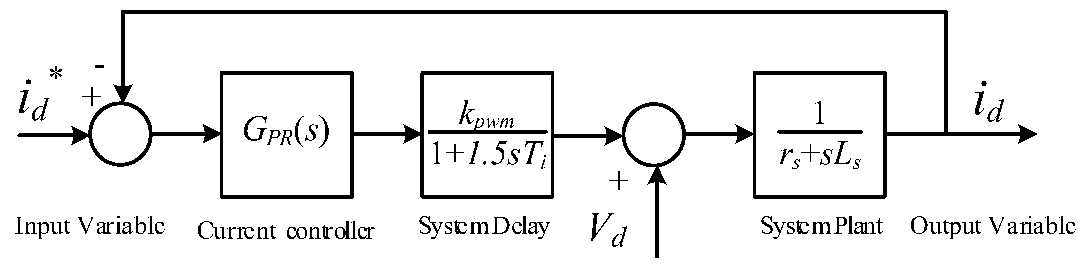
3.1. Current Loop Design on the Input Side

Equation (20) reveals the symmetry between the id current loop and the iq current loop. The same design methodology can be applied when designing the current loop. Considering that the command signal for the current control loop originates from the voltage control loop, it is essential to prevent current distortion caused by grid voltage fluctuations. Therefore, the current controller adopts a quasi-proportional resonance controller. The current loop operates with a sampling period denoted as Ti. It takes into account the characteristics of calculation delay and zero-order hold, and the PWM control is treated as a low-inertia component. Consequently, the structure of the id current loop in the dq coordinate system is depicted in Figure 7.
Neglecting the influence of power supply disturbances, we can derive the open-loop transfer function of the id current loop as follows:
i d * = k p 2 + k i 2 s v smref v sm i q * = 0 ,
where the equivalent gain of PWM control kpwm = 1, GPR (s) can be expressed as follows:
G PR ( s ) = k p + 2 k r ω c s s 2 + 2 ω c s + ω g 2 ,

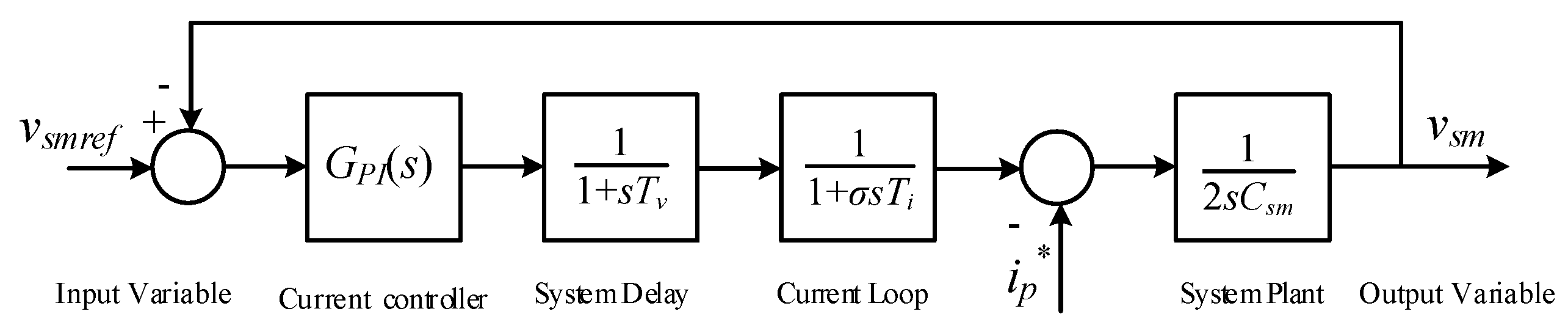
3.2. Submodule Voltage Loop Design on the Input Side

Equation (20) highlights the direct correlation between the transfer of active energy and the voltage across the capacitors. In the overall control perspective, the design of the voltage loop aims to determine the required current to stabilize the average submodule capacitance voltage at the desired value. Assuming the sampling period of the voltage loop as Tv, the voltage controller adopts a PI controller, and the current loop can be represented as a first-order inertia link, denoted as Gi(s). Figure 8 illustrates the structure of the voltage loop in the dq coordinate system.
Neglecting disturbances, the open-loop transfer function of the submodule voltage loop can be expressed as follows:
G 2 ( s ) = G PI ( s ) 2 s C sm 1 + s ( T v + σ T s ) ,

4. Design and Simulation

4.1. Input-Side Inductance Value Selection

The filter inductance value on the input side plays a crucial role in enabling the four-quadrant operation of the converter while ensuring satisfactory tracking performance of transient currents and effective suppression of harmonic currents. Specifically, for the A-phase circuit, neglecting the network-side resistance rs, Equation (1) can be simplified to a more concise form:
L s d d t i a = v a v a , lf ,
Figure 9 illustrates the vector relationship diagram under steady-state conditions. It reveals that by precisely controlling the amplitude and phase of the voltage component va,lf of the bridge arm, the converter can achieve four-phase limited operation.
Taking into account the phase relationships among the vectors depicted in Figure 9, the cosine theorem is employed to derive the following equation:
v a , lf 2 = v a 2 + ω 2 L s 2 i a 2 2 ω L s v a i a cos θ = v a 2 + ω 2 L s 2 i a 2 2 ω L s v a i a sin φ ,
After arithmetic operations, one can obtain the following:
L s = V a sin φ + V a 2 sin 2 φ + v a , lf 2 V a 2 ω i a = V m sin φ + V m 2 sin 2 φ + V a , lf , m 2 V m 2 ω I m ,
The maximum utilization rate of phase voltage is represented as M (M = 1/2 when SPWM is employed). Therefore, the voltage component va,lf and vsm must satisfy the condition Va,lf,max ≤ M n vsm. Based on this constraint, the value of Ls can be determined as follows:
L s V m sin φ + V m 2 sin 2 φ + M 2 n 2 v sm 2 V m 2 ω I m ,
When the inductor current is at its zero crossing point, it exhibits the highest rate of change, necessitating a sufficiently small inductance value to ensure fast current tracking. Figure 10a illustrates the waveform during a switching period near the zero crossing point of the inductive current. Throughout the entire period, the value of va is zero. For the interval 0 ≤ t ≤ T1, where Ls dia/dt > 0 and sa,lf = −1, the change in current is denoted as Δi1. During the period T1 ≤ t ≤ Ts, where Ls dia/dt < 0 and sa,lf = 1, the duration is labeled as T2, and the change in current is represented as Δi2.
L s Δ i 1 T 1 = n v sm , L s Δ i 2 T 2 = n v sm ,
The conditions that satisfy the current tracking rapidity are as follows:
Δ i 1 Δ i 2 T s I m s i n ω g T s T s ,
By using the above equation, the range of values of inductance Ls can be obtained as
L s n v sm 2 T 1 T s I m ω 0 T s ,
When the inductor current reaches its peak, the pulsation of harmonic current is most pronounced. Therefore, the inductance value should be sufficiently large to effectively suppress harmonic current. Figure 10b illustrates the waveform of the inductor current during a switching period near its peak value. Throughout the entire period, the value of va is Vm. For the interval 0 ≤ t ≤ T3, where Ls dia/dt > 0 and sa,lf = −1, the change in current is denoted as Δi3. During the period T3 ≤ t ≤ Ts, where Ls dia/dt < 0 and sa,lf =1, the duration is labeled as T4, and the change in current is represented as Δi4.
L s Δ i 3 T 3 = V m + n v sm L s Δ i 4 T 4 = V m n v sm ,
By applying the equation Δi3 + Δi4 = 0, the value of T3 can be expressed as follows:
T 3 = n v sm V m 2 n v sm T s ,
If the peak value of harmonic current is set as Δimax, the value range of Ls can be obtained by the inequality Δi3 ≤ Δimax.
L s n v sm 2 V m 2 2 n v sm Δ i max T s ,

4.2. Current Loop Design on the Input Side

The voltage range of the A-phase bridge arm is [−n vsm n vsm], where vsm represents the nominal voltage of the submodule. The total number of submodules in the cascade link is denoted as n.
n v a , lf , max + v hf , max v sm , ref ,
where vhf,max = kT vdc. va,lf,max can be obtained with the following:
v a , lf , max = V m 2 + ω g 2 L s 2 I m 2 = V m 2 + ω g 2 L s 2 2 P a V a , RMS 2 ,
Let the network-side current be the following:
i a = I m cos ( ω g t ) i b = I m cos ( ω g t 2 π / 3 ) i c = I m cos ( ω g t + 2 π / 3 ) ,
When the switching frequency significantly exceeds the fundamental frequency of the grid electromotive force, the harmonic components introduced by pulse width modulation (PWM) can be neglected. In this case, the duty ratio dk,lf can be expressed as follows:
d a , lf = λ m cos ( ω g t θ ) d b , lf = λ m cos ( ω g t θ 2 π 3 ) d c , lf = λ m cos ( ω g t θ + 2 π 3 ) ,
For phase A, neglecting the high-frequency component, the fundamental frequency double component and DC component of the capacitor current in the cascade submodule can be derived from Equation (9).
i sm = d a , lf i a = λ m I m 2 cos ( 2 ω g t θ ) + cos ( θ ) ,
Then, the maximum frequency doubling fluctuation of capacitor voltage caused by fundamental AC output is as follows:
Δ v sm , max = λ m I m 2 C sm cos ( 2 ω g t θ ) d t max = λ m I m 4 ω 0 C sm ,
The value range of Csm can be obtained.
C sm λ m I m 4 Δ v sm , max ω g

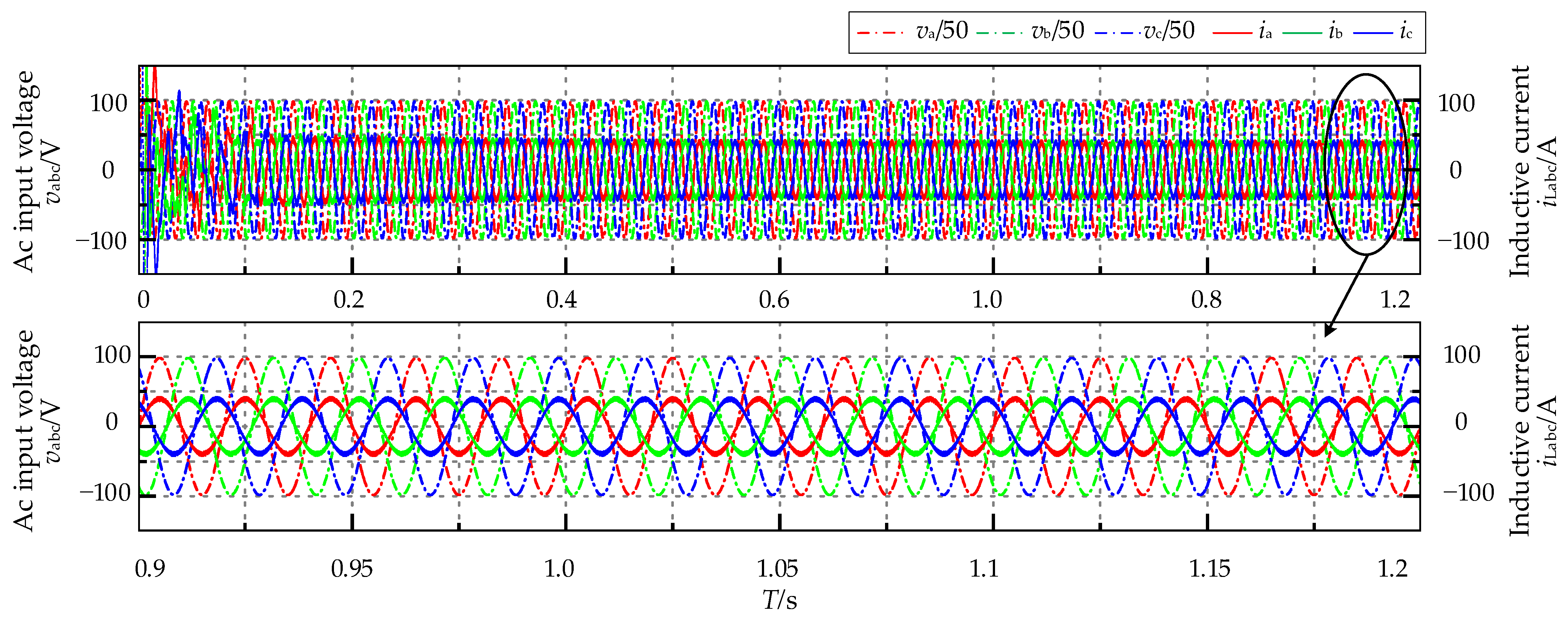
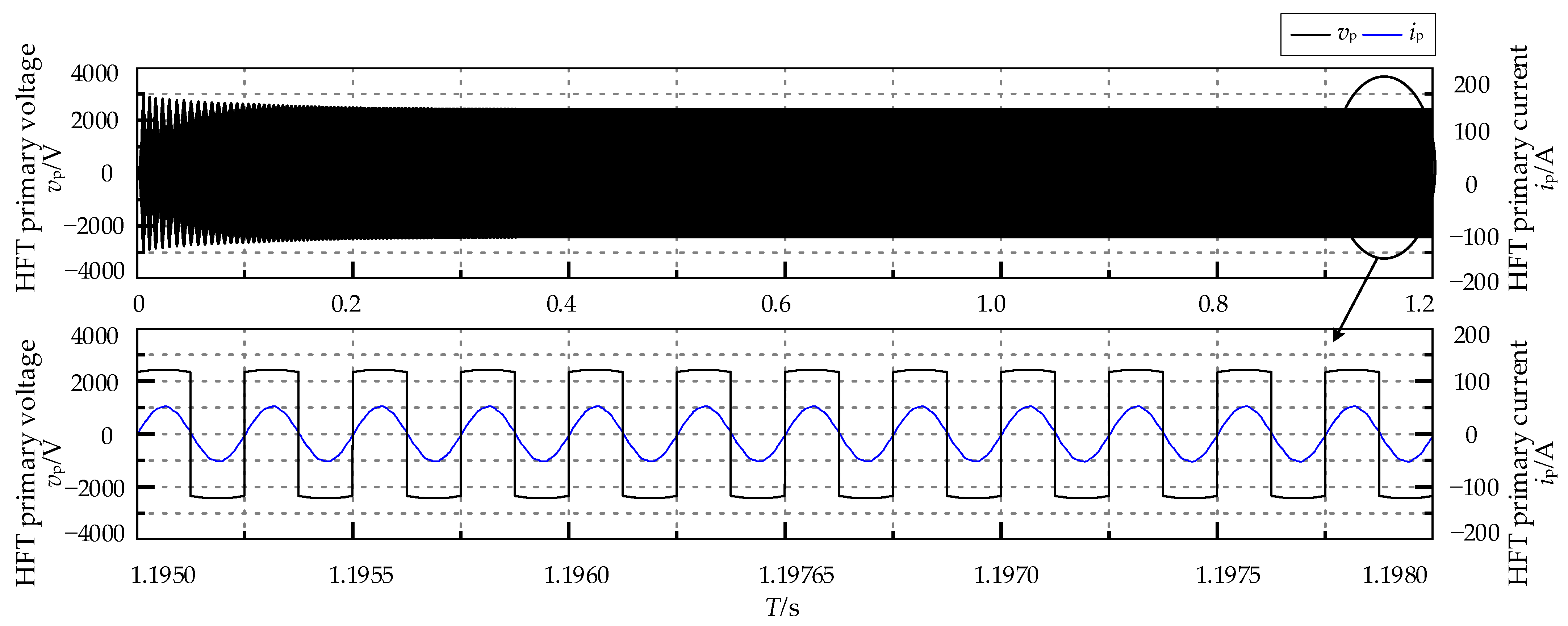
4.3. Simulation Analysis

In order to evaluate the effectiveness of the new topology in 6 kV (50 Hz) distribution networks, simulation models of CHB-PET, including PET-I based on the new topology and PET-II based on the conventional topology, are designed in this paper, and the corresponding simulation models are built using PLECS 4.1 software. Some parameters of the simulation models are shown in Table 1.
Figure 11, Figure 12, Figure 13, Figure 14 and Figure 15 depict the simulation results for some physical quantities on the primary and secondary sides of PET-I and PET-II. Specifically, Figure 11 gives the waveforms of the three-phase currents and voltages on the AC side of the PET-I. It is clear that the peak value of the current is 40.8 A and the power factor is kept at 1. An FFT analysis of the AC side current was also performed, and the results show that the THD is 4.6%.
The capacitor voltages in PET-I and PET-II are given in Figure 12 and Figure 13. Figure 12 shows the capacitor voltage waveforms of the input-side sub-module of PET-I and the input-side capacitor voltage of PET-II, and the simulation results show that the input-side capacitor voltages of both PET-I and PET-II are maintained at the design value of 750 V, which satisfies the design requirements. Figure 13 shows the output-side capacitor voltages of PET-I and PET-II, and the simulation results show that the output-side voltages of PET-I and PET-II are kept at the design value of 750 V, which meets the design requirements. The maximum voltage fluctuation of the input-side capacitor voltage of PET-I can be seen from the local zoomed-in figure to be 20 V, and the maximum ripple of the output-side capacitor voltage to be 10 V, which both satisfy the design requirements, so the new structure of PET-I can be considered to have practical value. It can also be seen that compared with PET-II, the control method in PET-I has deficiencies in robustness and stabilization speed. Therefore, the control method of PET-I needs to be further optimized, which will be the next research direction.
Figure 14 gives the voltage and current waveforms and local amplification waveforms of the primary side of the A-phase HFT in PET-I. The voltage and current have the same frequency, and the h-bridge switching tube at the output side is in a zero-current switching state. It was determined through the previous analysis that the high-frequency component vhf of the h-bridge arm voltage at the input side is equivalent to the HFT primary voltage. From Figure 14, the maximum value of the voltage vhf can be seen to be 2400 V. The modulation ratio of the PET is calculated to be 0.81.
Lastly, Figure 15 shows the duty cycle waveform of the h-bridge on the input side in PET-I. The duty cycle of the a-phase circuit can be divided into da,lf and dhf, where da,lf have a frequency of 50 Hz and dhf has a frequency of 4 kHz. In this phase, the bridge arm voltage can be divided into two components: a sinusoidal waveform va,lf and a square waveform vhf. The frequency of these voltages corresponds to the frequency of the da,lf and dhf frequencies.

5. Conclusions

This paper introduces a novel three-phase power electronic transformer (PET) topology. Building upon the existing cascaded H-Bridge PET (CHB-PET) structure, this topology enhances the input series output parallel (ISOP) configuration through the efficient reuse of H-bridges. Consequently, it significantly reduces the number of power switch tubes and high-frequency transformers employed in the entire system. The proposed topology not only maintains the DC bus port of the PET machine but also lowers hardware costs and minimizes the overall volume. Moreover, it effectively enhances the power density and compactness of the PET system. The unit power operation on the input side is achieved through power feedforward decoupling control. By employing series resonance, the H-bridge zero current switching (ZCS) operation on the output side can be realized with straightforward control techniques. As a result, the control strategy of the novel PET topology is simplified, making it highly suitable for widespread application.
Future research efforts will focus on exploring voltage equalization strategies in scenarios where there are discrepancies in submodule circuit parameters. Additionally, circuit analysis will be conducted to examine the impact of phase loss on the input side of the grid and non-resistive loads on the output side. These investigations will further enhance the understanding and performance of the proposed PET topology.

Author Contributions

Conceptualization, B.H., Y.L., Z.Y. and Y.T.; methodology, B.H. and Y.L.; software, B.H.; validation, B.H.; formal analysis, B.H.; investigation, B.H.; resources, B.H.; data curation, B.H.; writing, B.H.; visualization, Z.Y. and Y.L.; supervision, Z.Y.; project administration, Y.L. and Y.T. All authors have read and agreed to the published version of the manuscript.

Funding

This research received no external funding.

Data Availability Statement

The data used to support the findings of this study are included in the article.

Conflicts of Interest

The authors declare no conflict of interest.

References

  1. Chen, X.; Liu, Y.; Zhang, Y. Pathway toward carbon-neutral power systems in China. iEnergy 2022, 1, 9–10. [Google Scholar] [CrossRef]
  2. Khazaei, J.; Nguyen, D.H. Multi-Agent Consensus Design for Heterogeneous Energy Storage Devices With Droop Control in Smart Grids. IEEE Trans. Smart Grid 2019, 10, 1395–1404. [Google Scholar] [CrossRef]
  3. Huang, A.; Crow, M.; Heydt, G.; Zheng, J.; Dale, S. The Future Renewable Electric Energy Delivery and Management (FREEDM) System: The Energy Internet. Proc. IEEE 2011, 99, 133–148. [Google Scholar] [CrossRef]
  4. Huang, A.Q. Medium-voltage solid-state transformer: Technology for a smarter and resilient grid. IEEE Ind. Electron. Mag. 2016, 10, 29–42. [Google Scholar] [CrossRef]
  5. She, X.; Huang, A.Q.; Burgos, R. Review of Solid-State Transformer Technologies and Their Application in Power Distribution Systems. Emerg. Sel. Top. Circuits Syst. 2013, 1, 186–198. [Google Scholar]
  6. Huang, A.Q.; Zhu, Q.; Wang, L.; Zhang, L. 15 kV SiC MOSFET: An enabling technology for medium voltage solid state transformers. CPSS Trans. Power Electron. Appl. 2017, 2, 118–130. [Google Scholar] [CrossRef]
  7. Briz, F.; Lopez, M.; Rodriguze, A.; Arias, M. Modular power electronic transformers: Modular multilevel converter versus cascaded H-bridge solutions. IEEE Ind. Electron. Mag. 2016, 10, 6–19. [Google Scholar] [CrossRef]
  8. Vasiladiotis, M.; Rufer, A. A Modular Multiport Power Electronic Transformer With Integrated Split Battery Energy Storage for Versatile Ultrafast EV Charging Stations. IEEE Trans. Ind. Electron. 2014, 62, 3213–3222. [Google Scholar] [CrossRef]
  9. Deswal, D.; De León, F. Distributed Dual Model for High-Frequency Transformer Windings: Electromagnetic Transients and Solid State Transformers. IEEE Open Access J. Power Energy 2022, 9, 549–559. [Google Scholar] [CrossRef]
  10. Dujic, D.; Zhao, C.; Mester, A.; Steinke, J.; Weiss, M.; Lewdeni, S.; Chaudhuri, T.; Stefanutti, P. Power Electronic Traction Transformer-Low Voltage Prototype. IEEE Trans. Power Electron. 2013, 28, 5522–5534. [Google Scholar] [CrossRef]
  11. Madhusoodhanan, S.; Tripathi, A.; Patel, D.; Mainali, K.; Kadavelugu, A.; Hazra, S.; Bhattacharya, S.; Hatua, K. Solid State Transformer and MV grid tie applications enabled by 15 kV SiC IGBTs and 10 kV SiC MOSFETs based multilevel converters. IEEE Trans. Ind. Appl. 2015, 51, 3343–3360. [Google Scholar] [CrossRef]
  12. Wang, J.; Luo, F.; Duan, Q.; Ji, Z.; Gu, B.; You, J.; Gu, W.; Zhao, J. Power electronic transformer with adaptive PLL technique for voltage-disturbance ride through. J. Mod. Power Syst. Clean Energy 2018, 6, 1090–1102. [Google Scholar] [CrossRef]
  13. Wang, D.; Tian, J.; Mao, C.; Lu, J.; Duan, Y.; Qiu, J.; Cai, H. A 10-kV/400-V 500-kVA Electronic Power Transformer. IEEE Trans. Ind. Electron. 2016, 63, 6653–6663. [Google Scholar] [CrossRef]
  14. Zheng, G.; Chen, Y.; Kang, Y. Modeling and control of the modular multilevel converter (MMC) based solid state transformer (SST) with magnetic integration. CES Trans. Electr. Mach. Syst. 2020, 4, 309–318. [Google Scholar] [CrossRef]
  15. Wang, L.; Zhang, D.; Wang, Y.; Wu, B.; Athab, H.S. Power and Voltage Balance Control of a Novel Three-Phase Solid-State Transformer Using Multilevel Cascaded H-Bridge Inverters for Microgrid Applications. IEEE Trans. Power Electron. 2016, 31, 3289–3301. [Google Scholar] [CrossRef]
  16. Zhang, X.; Xu, Y.; Xiao, X. A High Power Density Resonance Cascaded H-Bridge Solid-State Transformer for Medium and High Voltage Distribution Network. Trans. China Electrotech. Soc. 2018, 33, 310–321. [Google Scholar] [CrossRef]
  17. Zhang, G.; Chen, J.; Zhang, B.; Zhang, Y. A critical topology review of power electronic transformers: In view of efficiency. Chin. J. Electr. Eng. 2018, 4, 90–95. [Google Scholar]
  18. Shu, L.; Chen, W.; Zhang, C. Power Electronic Transformer Based on Mixed-Frequency Modulation Strategy. In Proceedings of the 2019 10th International Conference on Power Electronics and ECCE Asia, Busan, Republic of Korea, 27–30 May 2019; pp. 1559–1564. [Google Scholar]
  19. Ma, D.; Chen, W.; Shu, L. A Multiport Three-stage Power Electronic Transformer. In Proceedings of the 2020 IEEE Applied Power Electronics Conference and Exposition, New Orleans, LA, USA, 15–19 March 2020; pp. 2285–2290. [Google Scholar]
  20. Zhang, J.; Liu, J.; Zhong, S.; Yang, J.; Zhao, N.; Zheng, T.Q. A Power Electronic Traction Transformer Configuration With Low-Voltage IGBTs for Onboard Traction Application. IEEE Trans. Power Electron. 2019, 34, 8453–8467. [Google Scholar] [CrossRef]
  21. Zhao, C.; Zhang, C.; Jiang, Q. An H-Bridge Time-Sharing Multiplexing-Based Power Electronic Transformer. IEEE J. Emerg. Sel. Top. Power Electron. 2023, 11, 4831–4840. [Google Scholar] [CrossRef]
  22. Mou, D.; Dai, Y.; Yuan, L.; Luo, Q.; Wang, H.; Wei, S.; Zhao, Z. Reactive Power Minimization for Modular Multi-Active-Bridge Converter With Whole Operating Range. IEEE Trans. Power Electron. 2023, 38, 8011–8015. [Google Scholar] [CrossRef]
  23. Velazquez-Ibañez, A.; Rodríguez-Rodríguez, J.R.; Santoyo-Anaya, M.A.; Arrieta-Paternina, M.R.; Torres-García, V.; Moreno-Goytia, E.L. Advanced PET Control for Voltage Sags Unbalanced Conditions Using Phase-Independent VSC-Rectification. IEEE Trans. Power Electron. 2021, 36, 11934–11943. [Google Scholar] [CrossRef]
  24. Feng, M.; Gao, C.; Ding, J.; Ding, H.; Xu, J.; Zhao, C. Hierarchical Modeling Scheme for High-Speed Electromagnetic Transient Simulations of Power Electronic Transformers. IEEE Trans. Power Electron. 2021, 36, 9994–10004. [Google Scholar] [CrossRef]
  25. Liu, H.; Ma, L.; Song, W.; Peng, L. An Internal Model Direct Power Control With Improved Voltage Balancing Strategy for Single-Phase Cascaded H-Bridge Rectifiers. IEEE Trans. Power Electron. 2022, 37, 9241–9253. [Google Scholar] [CrossRef]
  26. Pan, Y.; Teng, J.; Yang, C.; Bu, Z.; Wang, B.; Lin, X.; Sun, X. Capacitance Minimization and Constraint of CHB Power Electronic Transformer Based on Switching Synchronization Hybrid Phase-Shift Modulation Method of High Frequency Link. IEEE Trans. Power Electron. 2023, 38, 6224–6242. [Google Scholar] [CrossRef]
  27. Li, X.; Cheng, L.; He, L.; Wang, C.; Zhu, Z. Decoupling Control of an LLC-Quad-Active-Bridge Cascaded Power Electronic Transformer Based on Accurate Small-Signal Modeling. IEEE J. Emerg. Sel. Top. Power Electron. 2022, 10, 4115–4127. [Google Scholar] [CrossRef]
  28. Sun, Y.; Zhu, J.; Fu, C.; Chen, Z. Decoupling Control of Cascaded Power Electronic Transformer Based on Feedback Exact Linearization. IEEE J. Emerg. Sel. Top. Power Electron. 2022, 10, 3662–3676. [Google Scholar] [CrossRef]
  29. Zheng, L.; Marellapudi, A.; Chowdhury, V.; Kandula, R.; Saeedifard, M.; Grijalva, S.; Divan, D. Solid-State Transformer and Hybrid Transformer With Integrated Energy Storage in Active Distribution Grids: Technical and Economic Comparison, Dispatch, and Control. IEEE J. Emerg. Sel. Top. Power Electron. 2022, 10, 3771–3787. [Google Scholar] [CrossRef]
  30. Atkar, D.; Chaturvedi, P.; Suryawanshi, H.; Nachankar, P.; Yadeo, D.; Saketi, S. Three-Phase Integrated-Optimized Power Electronic Transformer for Electric Vehicle Charging Infrastructure. IEEE Trans. Ind. Appl. 2022, 58, 5198–5213. [Google Scholar] [CrossRef]
Figure 1. Traditional three-phase CHB-PET topology.
Electronics 13 00022 g001
Figure 2. Novel three-phase cascade PET topology.
Electronics 13 00022 g002
Figure 3. Evolution of the novel CHB-PET topologies. (a) The internal structure of the cascade unit; (b) sub-module equivalent circuit. (c) DAB equivalent circuit; (d) novel AC/DC converter structure combining (b,c).
Electronics 13 00022 g003
Figure 4. Equivalent circuit of the front stage of CHB-PET.
Electronics 13 00022 g004
Figure 5. The average model of the preceding circuit in the dq coordinate system.
Electronics 13 00022 g005
Figure 6. Control block diagram and control flow chart of the new CHB-PET.
Electronics 13 00022 g006
Figure 7. Current control loop structure.
Electronics 13 00022 g007
Figure 8. Voltage control loop structure.
Electronics 13 00022 g008
Figure 9. Input-side vector relationship under steady state condition.
Electronics 13 00022 g009
Figure 10. Inductive current waveform in a switching period. (a) Near zero current crossing; (b) near the peak of the current.
Electronics 13 00022 g010
Figure 11. AC-side input voltage waveform and inductive current waveform of the PET-I and local amplification.
Electronics 13 00022 g011
Figure 12. Output-side capacitor voltage waveform of the PET-I and PET-II and local amplification.
Electronics 13 00022 g012
Figure 13. Output-side capacitor voltage waveform of the PET-I and PET-II.
Electronics 13 00022 g013
Figure 14. HFT primary voltage and current waveform of the PET-I.
Electronics 13 00022 g014
Figure 15. The duty cycle waveform of the input-side H-bridge of the PET-I.
Electronics 13 00022 g015
Table 1. Parameters of the simulation models.
TypeParameterValues (Units)ParameterValues (Units)
PET-IGrid line voltage rms6 kVOutput-side DC voltage750 V
Input-side filter inductance9 mHOutput-side Capacitance15 mF
Ratio of HFT3.2LC filter inductance3.166 mH
Sub-module capacitance2 mFLC filter capacitance0.5 μF
Sub-module capacitance voltage750 VNumber of sub-modules on A phase12
PET-IIGrid line voltage rms6 kVOutput-side DC voltage750 V
Input-side filter inductance5 mHRatio of HFT1
Output-side capacitance2 mFNumber of HFT on A phase12
Output-side capacitance voltage750 VNumber of sub-modules on A phase12
Disclaimer/Publisher’s Note: The statements, opinions and data contained in all publications are solely those of the individual author(s) and contributor(s) and not of MDPI and/or the editor(s). MDPI and/or the editor(s) disclaim responsibility for any injury to people or property resulting from any ideas, methods, instructions or products referred to in the content.

