Article

Modeling and Experimental Validation of Dual-Output Flyback Converters with Capacitive Coupling for Improved Cross-Regulation

School of Aerospace Engineering, Sapienza, University of Rome, Via Salaria 851, 00138 Rome, Italy
*
Author to whom correspondence should be addressed.
Electronics 2024, 13(17), 3503; https://doi.org/10.3390/electronics13173503
Submission received: 29 July 2024 / Revised: 28 August 2024 / Accepted: 2 September 2024 / Published: 3 September 2024
(This article belongs to the Special Issue New Insights in Power Electronics: Prospects and Challenges)

Abstract

:
This paper addresses cross-regulation in dual-output flyback converters. An original analytical framework is developed to model the impact of a balancing capacitor connected among a transformer’s secondary windings in order to mitigate the cross-regulation among different outputs. To validate the proposed model, a prototype dual-output flyback converter was built and tested for a wide range of load unbalances. The measured cross-regulation error was compared with the theoretical predictions provided by the proposed model, obtaining a tight fit, which confirms the validity of the proposed approach.

1. Introduction

In the evolving domain of industrial electronics, the flyback converter stands out as a prominent topology for low-power applications, renowned for its galvanic isolation, minimal component count, wide output voltage range, ease of control, and cost-effectiveness [1,2,3,4,5,6,7]. The inherent isolation significantly contributes to the development of multi-output DC-DC power converters, which are essential for a variety of applications, including computing, television, telecommunications, and battery charging systems. Despite their widespread adoption [8,9], multi-output flyback converters face significant challenges in achieving effective cross-regulation, attributed to their complex dynamics and component non-idealities [10]. This phenomenon implies that variations in the load current of any output terminal result in corresponding changes in the output voltage of other terminals [11,12,13]. The leading factors contributing to cross-regulation include leakage inductances, along with transformer winding resistances and diode voltage drops. These elements collectively result in deviations in output voltages when load unbalances occur across different outputs [13,14,15,16].
A wide range of strategies, from post-regulation to active and passive solutions, was explored to mitigate the cross-regulation issue [10,12]. However, while post-regulation approaches may offer a straightforward solution for achieving tightly regulated outputs, they come with significant drawbacks. Linear post-regulators, even when employing low-dropout technology, are subject to considerable power losses that adversely affect overall system efficiency. On the other hand, switching post-regulators, despite their potential for higher efficiency, contribute to increased component count and system complexity, presenting challenges in design and integration [11,17]. Alternatively, active strategies use advanced techniques, such as replacing or augmenting output diodes with active switching devices for improved regulation [18,19]. Several configurations using multiple transformers have also been proposed to improve cross-regulation [20,21,22]. However, active approaches significantly increase complexity and component count, challenging the balance between regulation, efficiency, and power density.
Conversely, passive methods aim to enhance regulation without increasing complexity, by transformer winding optimization [23] or by using stacked transformer windings and stacked outputs [24,25]. While these methods can reduce cross-regulation, they may complicate the implementation of synchronous rectification. The weighted-feedback method spreads the error across all outputs, trading off precision for reduced cross-regulation [26,27].
Capacitive coupling, a straightforward passive technique involving capacitors connected across output pairs, has found application in multi-output flyback converters, where the output voltages are equal in magnitude [28].
Despite its common usage, there is a notable absence of a detailed analytical framework in the literature that directly links the amplitude of cross-regulation with load imbalances. Addressing this gap, this study aims to establish a comprehensive model of a dual-output flyback converter featuring capacitive coupling under unbalanced output current loads. The interplay between leakage inductances, bridging capacitors, and their impact on output cross-regulation is thoroughly analyzed.
Section 2 details an analytical approach for deriving the converter model, elucidating the inherent mechanism for cross-regulation in flyback converters and examining its critical factors. Section 3 presents the experimental results obtained by characterizing a prototype built to validate the derived key points.

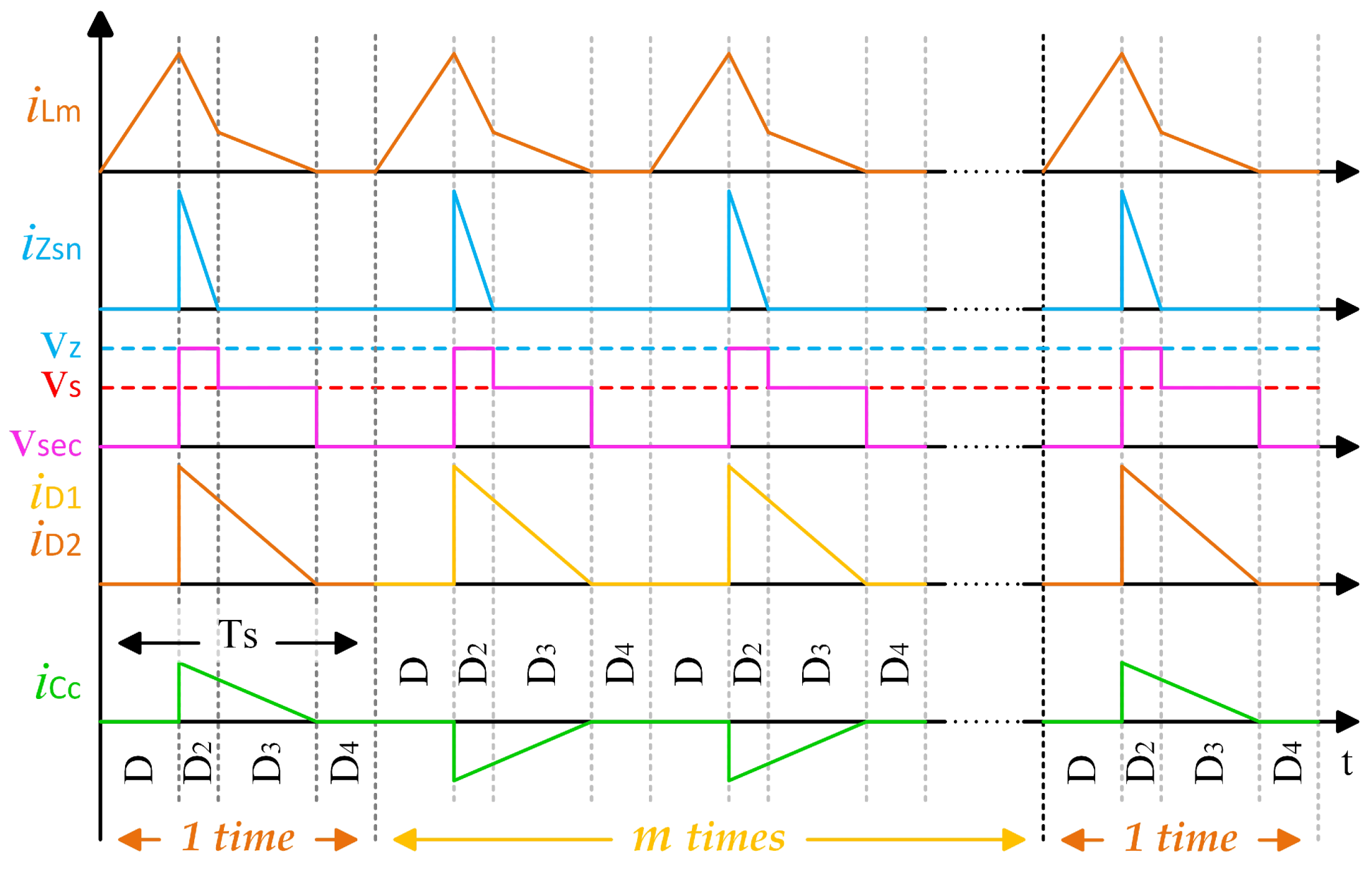
2. Dual-Output Flyback Converter

A flyback converter cyclically stores energy in its transformer from the input DC source when its switch is on and subsequently delivers this stored energy to its outputs after the switch is turned off. By adjusting the amount of energy stored and released per cycle, the output voltage can be regulated. Figure 1 illustrates a typical two-output flyback converter topology featuring a zener-diode.
In Figure 1 is represented the transformer model with a magnetizing inductance, L m ; and equivalent leakage inductances L k p , L k 1 , and L k 2 ; along with winding resistances R w p , R w 1 , and R w 2 , corresponding to those of the primary and secondary windings, respectively. The turns ratios of the secondary windings with respect to the primary winding are n 1 and n 2 values, respectively. In standard flyback converters, when the load on output 2 of the converter is different from that on output 1, a voltage mismatch arises, mainly due to the transformer’s output leakage inductances [12,13]. To address this issue, a balancing capacitor, C C , is introduced between the two transformers’ output windings [28]. This capacitor provides an alternative discharge path for excess current from the lightly loaded output’s secondary winding to the more heavily loaded output. For this solution to effectively enhance cross-regulation, it is crucial that the C C capacitor’s terminals are connected between secondary windings exhibiting similar waveforms. This requirement specifies equal turns on both output windings. Additionally, a balanced dual-output voltage topology can be achieved by connecting the positive terminal of one output to the ground and keeping the balancing capacitor across the anodes of both output rectifying diodes.
In the analytical modeling, the forward voltage of the output rectifier diodes D O 1 and D O 2 is initially neglected. Furthermore, to simplify the analysis, the primary winding leakage inductance L k p is neglected in calculations, as its primary effect lies in the energy transferred to the secondary side [29]. Its impact on output cross-regulation is thus minimal, and can eventually be reintroduced at a later stage for converter gain calculation. Conversely, the coupling between the output windings significantly influences the output voltage, as it is determined by the current through different windings and the leakage inductances [24,30]. Consequently, leakage inductance in the secondary sides of the transformer directly affects the cross-regulation under unbalanced load conditions.

Analytical Modeling

The load current ratio between the two outputs can be expressed as m = I O 2 I O 1 . In a steady state, circuit currents and voltages remain constant, allowing us to estimate their averages over multiple switching periods. Specifically, we find it convenient to consider m + 1 periods. Due to the presence of the C C capacitor, it is convenient to model the operation of the circuit by assuming that for m periods current flows towards the output 1 through diode D O 1 , and for one period towards the lightly loaded output 2 through diode D O 2 . It is important to note that this model can be deemed valid if the balancing capacitor C C is selected to be sufficiently large, ensuring that the resonance frequency of the series equivalent circuit comprising the leakage inductances L k 1 , L k 2 , and C C is significantly lower than the switching frequency f s . This prerequisite is essential for enabling the series circuit to act as a capacitive impedance, thereby establishing a low-impedance pathway for the flow of the balancing current.
f r = 1 2 π ( L k 1 + 1 m L k 2 ) · C C f s
Under this condition, the current waveforms of this model can be plotted for m + 1 switching cycles, as illustrated in Figure 2, when operating in discontinuous conduction mode (DCM), without loss of generality. Likewise, the various subintervals can be identified as illustrated in Figure 3.
During the first subinterval of duration D T S , as illustrated in Figure 3a, the switch S 1 is closed and the magnetizing current is increasing according to
i L m ( t ) = V i n L m t
During this period, while the output rectifying diodes remain open, the output capacitors C O 1 and C O 2 discharge to supply respective outputs. Simultaneously, the balancing capacitor C C discharges through both secondary windings of the transformer. Given that the ratio between the two transformer secondary sides is ideally equal ( n 1 = n 2 = n ), the voltages on the secondary windings have identical amplitudes equal to the input voltage. Consequently, the C C balancing capacitor undergoes a discharge, which can be described as
i C c ( t ) = i L k 2 ( t ) = i L k 1 ( t ) = v C c ( t ) L k 1 + L k 2 t
During the second subinterval of duration D 2 T S , as shown in Figure 3b, the switch S 1 opens, and the zener diode Z S N clamps the voltage on the transformer’s primary side to the zener voltage V Z . Consequently, the magnetizing current decreases according to
i L m ( t ) = V Z n L m t
During this subinterval, we can distinguish between the times when the output diode D O 1 is in conduction ( m m + 1 times) and when the output diode D O 2 is in conduction ( 1 m + 1 times). When D O 1 conducts, the balancing capacitor C C redirects the current from the secondary winding of output 2 to output 1. Both windings reflect the clamped voltage V Z multiplied by the turn ratio n. The current through C C can be expressed as a function of the output voltages and the voltage across C C itself.
i C c ( t ) = i L k 2 ( t ) = n V Z V O 1 + v C c ( t ) L k 2 t
Meanwhile, the leakage inductance on the secondary winding of output 1 charges according to
i L k 1 ( t ) = n V Z V O 1 L k 1 t
Moreover, the capacitor on output 2 sustains the output current I O 2 by itself, whereas the capacitor on output 1 also receives the current flowing through the output diode D O 2 .
i C O 1 ( t ) = [ n V Z V O 1 L k 1 + n V Z V O 1 + v C c ( t ) L k 2 I O 1 ] t
When the output diode D O 2 conducts, the balancing capacitor C C redirects the current from the secondary winding of output 1 to output 2. The current through C C can now be expressed as
i C c ( t ) = i L k 1 ( t ) = n V Z V O 2 v C c ( t ) L k 1 t
Meanwhile, the leakage inductance on the secondary winding of output 2 charges according to
i L k 2 ( t ) = n V Z V O 2 L k 2 t
This time, the capacitor on output 1 sustains the output current entirely by itself, while the capacitor on output 2 also receives the current flowing through the output diode D O 2 .
i C O 2 ( t ) = [ n V Z V O 2 L k 2 + n V Z V O 2 v C c ( t ) L k 1 I O 2 ] t
This subinterval ends when the current through the zener clamping diode drops to zero, after a decrease that equals the current reached by the magnetizing inductance during its charging, according to Equation (2). This can be expressed as
V I N L m D T S [ V Z n L m + n V Z V O 1 L k 1 + n V Z V O 2 L k 2 ] D 2 T S = 0
During the third subinterval of duration D 3 T S , the primary side of the transformer is no longer clamped to the zener voltage. Consequently, a voltage V S is established across both the transformer secondary windings until the magnetizing inductance is completely discharged. Hence, the magnetizing current discharges according to
i L m ( t ) = V S n L m t
During this subinterval, the behavior of the converter is the same as in the second subinterval for both 1 m + 1 and m m + 1 periods. Accordingly, the equations for i L k 1 , i L k 2 , i C C , i C O 1 , and i C O 2 , written for the second subinterval, still hold by replacing V Z with V S .
Finally, during the fourth subinterval of duration D 4 T S , the magnetizing inductance L m is completely discharged, and no current flows through the primary side of the transformer. Similar to the first subinterval, the output capacitors C O 1 and C O 2 supply the load currents, while the balancing capacitor C C discharges through both secondary windings of the transformer, as described in Equation (3).
By considering the average values of all variables over m + 1 switching periods, and making some simplifying assumptions, such as L k 1 = L k 2 = L k and n = 1 , it is possible to write the system of Equation (13).
I L k 1 = V C c 2 L k ( D + D 4 ) + [ m V Z V O 1 L k + V Z V O 2 V C c L k ] D 2 m + 1 + [ m V S V O 1 L k + V S V O 2 V C c L k ] D 3 m + 1 = 0 I L k 2 = V C c 2 L k ( D + D 4 ) + [ m V Z V O 1 + V C c L k + V Z V O 2 L k ] D 2 m + 1 + [ m V S V O 1 + V C c L k + V S V O 2 L k ] D 3 m + 1 = 0 I C O 1 = I O 1 + m m + 1 [ V Z V O 1 L k + V Z V O 1 + V C c L k ] D 2 + m m + 1 [ V S V O 1 L k + V S V O 1 + V C c L k ] D 3 = 0 I C O 2 = I O 2 + [ V Z V O 2 L k + V Z V O 2 V C c L k ] D 2 m + 1 + [ V S V O 2 L k + V S V O 2 V C C L k ] D 3 m + 1 = 0 I C C = V C c 2 L k ( D + D 4 ) + [ V Z V O 2 V C c L k m V Z V O 1 + V C c L k ] D 2 m + 1 + [ V S V O 2 V C c L k m V S V O 1 + V C c L k ] D 3 m + 1 = 0 I Z S N = V i n L m D [ V Z L m + V Z V O 1 L k + V Z V O 2 L k ] D 2 = 0 I L m = V i n L m D V Z n L m D 2 V S n L m D 3 T S = 0
By calculating I L k 2 I L k 1 , we obtain
V C c L k ( D + D 4 ) + V C c L k ( D 2 + D 3 ) = 0
and by taking into account that D + D 2 + D 3 + D 4 = 1 , it is determined that the average of v C C ( t ) is
V C c = 0
By deriving D 2 from Equation (13), substituting it into the other equations, and considering Equation (15), we can simplify the system of Equation (13) to obtain the system of Equation (16).
I L k 1 = V i n D ( V O 1 m m + 1 + V O 2 1 m + 1 ) ( D 3 + V i n V Z D V S V Z D 3 ) = 0 I C O 1 = I O 1 m + 1 m L k 2 + V i n D V O 1 ( D 3 + V i n V Z D V S V Z D 3 ) = 0 I C O 2 = I O 2 ( m + 1 ) L k 2 + V i n D V O 2 ( D 3 + V i n V Z D V S V Z D 3 ) = 0 I Z S N = V i n D [ 1 L m + 2 L k V O 1 V Z L k V O 2 V Z L k ] ( V i n D V S D 3 ) = 0 I C C = ( 1 m ) V i n D + ( m V O 1 V O 2 ) ( D 3 + V i n V Z D V S V Z D 3 ) = 0
By computing I C C + m I C O 1 , we obtain
I O 1 ( m + 1 ) L k 2 V i n D + V O 2 ( D 3 + V i n V Z D V S V Z D 3 ) = 0
from which the expression for V O 2 can be derived.
V O 2 = V i n D I O 1 ( m + 1 ) L k 2 D 3 + V i n V Z D V S V Z D 3
By substituting the obtained expression for V O 2 into I C C , we obtain
I O 1 ( m + 1 ) L k 2 m V i n D + m V O 1 ( D 3 + V i n V Z D V S V Z D 3 ) = 0
from which the expression for V O 1 can also be derived.
V O 1 = m V i n D I O 1 ( m + 1 ) L k 2 m ( D 3 + V i n V Z D V S V Z D 3 )
Provided that the second terms in the numerators of expressions for V O 1 and V O 2 are negligible, for the sake of solving the system equations, we can neglect their difference and assume that V O 1 V O 2 = V O 1 , 2 . Hence, we can write
V O 1 , 2 = V i n D D 3 + V i n V Z D V S V Z D 3
By substituting the obtained values for D 2 , V O 1 , and V O 2 into the I Z S N equation, we can derive the expression for D 3 .
D 3 = V i n D [ 2 V Z L m V S ( L k + 2 L m ) ] V S ( V Z V S ) ( L k + 2 L m )
Thus, by substituting the derived expression for D 3 back into the derived expression for V O 1 (Equation (20)), we can obtain the expression for V S .
V S = 2 V O 1 L m L k + 2 L m
P i n = V i n i i n ( t ) = V i n Q i n T S = V i n 1 2 D T S V i n D T S L m T S = V i n 2 D 2 T S 2 L m P Z S N = V Z i Z S N ( t ) = V Z Q Z T S = V Z 1 2 D 2 T S V i n D T S L m T S = V i n V Z D D 2 T S 2 L m P o u t = V O 1 I O 1 + V O 2 I O 2 = V O 1 , 2 ( I O 1 + I O 2 )
By imposing the power balance P i n = P Z S N + P o u t , and expressing the averaged values for input and zener currents in terms of the overall charge Q flowing along an entire switching period T S , we can achieve the set of Equation (24).
By substituting the obtained values for D 2 and D 3 , it is finally possible to derive the expression for the duty cycle D as a function of all specified design parameters, which include the output voltages V O 1 , 2 , output currents I O 1 and I O 2 , the zener diode clamping voltage V Z , input voltage V i n , the switching frequency f s = 1 T S , and the magnetizing and leakage inductances L m and L k , respectively.
D = V O 1 , 2 ( I O 1 + I O 2 ) ( V Z ( L k + 2 L m ) 2 V O 1 , 2 L m ) ( V Z V O 1 , 2 ) V i n 2 T S
In the general case where L k 1 L k 2 , the set of equations can be similarly derived as in the system of Equation (2).
V O 2 = V i n D I O 1 ( m + 1 ) L k 1 L k 2 L k 1 + L k 2 D 3 + V i n V Z D V S V Z D 3 V O 1 = m V i n D I O 1 ( m + 1 ) L k 1 L k 2 L k 1 + L k 2 m ( D 3 + V i n V Z D V S V Z D 3 ) D 3 = V i n D [ V Z L m V S ( L k 1 L k 2 L k 1 + L k 2 + L m ) ] V S ( V Z V S ) ( L k 1 L k 2 L k 1 + L k 2 + L m ) V S = V O 1 , 2 L m L k 1 L k 2 L k 1 + L k 2 + L m D = V O 1 , 2 ( I O 1 + I O 2 ) ( V Z ( L k 1 L k 2 L k 1 + L k 2 + 2 L m ) 2 V O 1 , 2 L m ) ( V Z V O 1 , 2 ) V i n 2 T S
Since the balancing capacitor has a zero-mean voltage over a switching period (Equation (15)), the two output voltages can be considered equal, as shown in Equation (21). However, if the voltage drops V D O 1 ( I O 1 ) and V D O 2 ( I O 2 ) across the output rectifying diodes are taken into account, even with a null average voltage on the balancing capacitor C C , a voltage difference is actually expected to appear on the output nodes, due to the unbalanced currents on rectifying diodes. Accordingly, it is possible to write
V O 1 = v x ( t ) V D O 1 ( I O 1 ) V O 2 = v y ( t ) V D O 2 ( I O 2 )
Since v x ( t ) = v y ( t ) owing to the zero average voltage across the C C balancing capacitor, we can write
V O 2 = V O 1 + V D O 1 ( I O 1 ) V D O 2 ( I O 2 )
Hence, the discrepancy in output voltages can be attributed directly to the voltage drops across the output rectifying diodes.

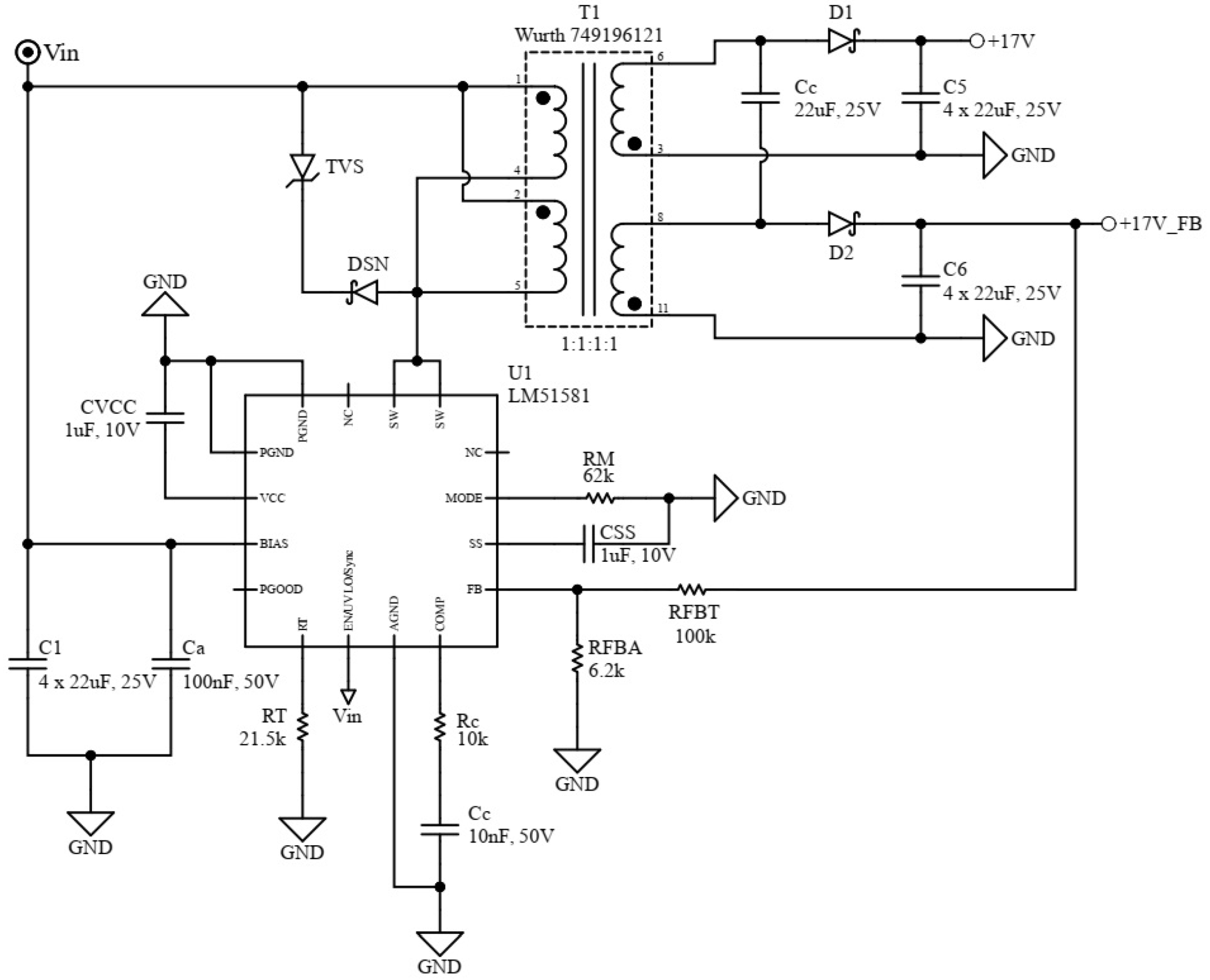
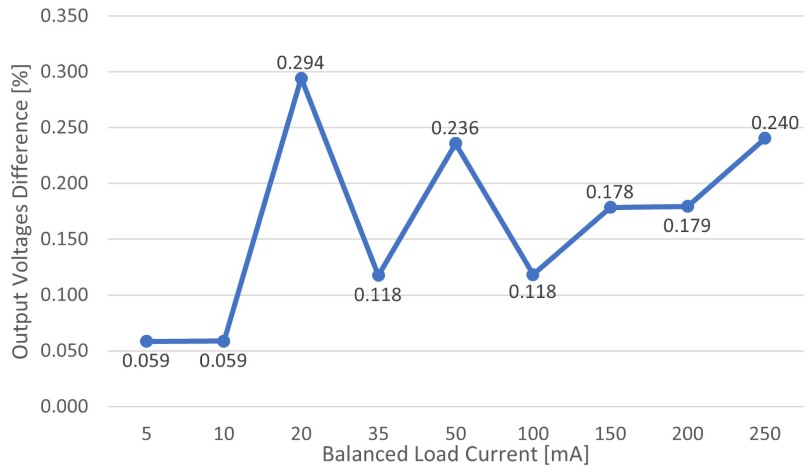
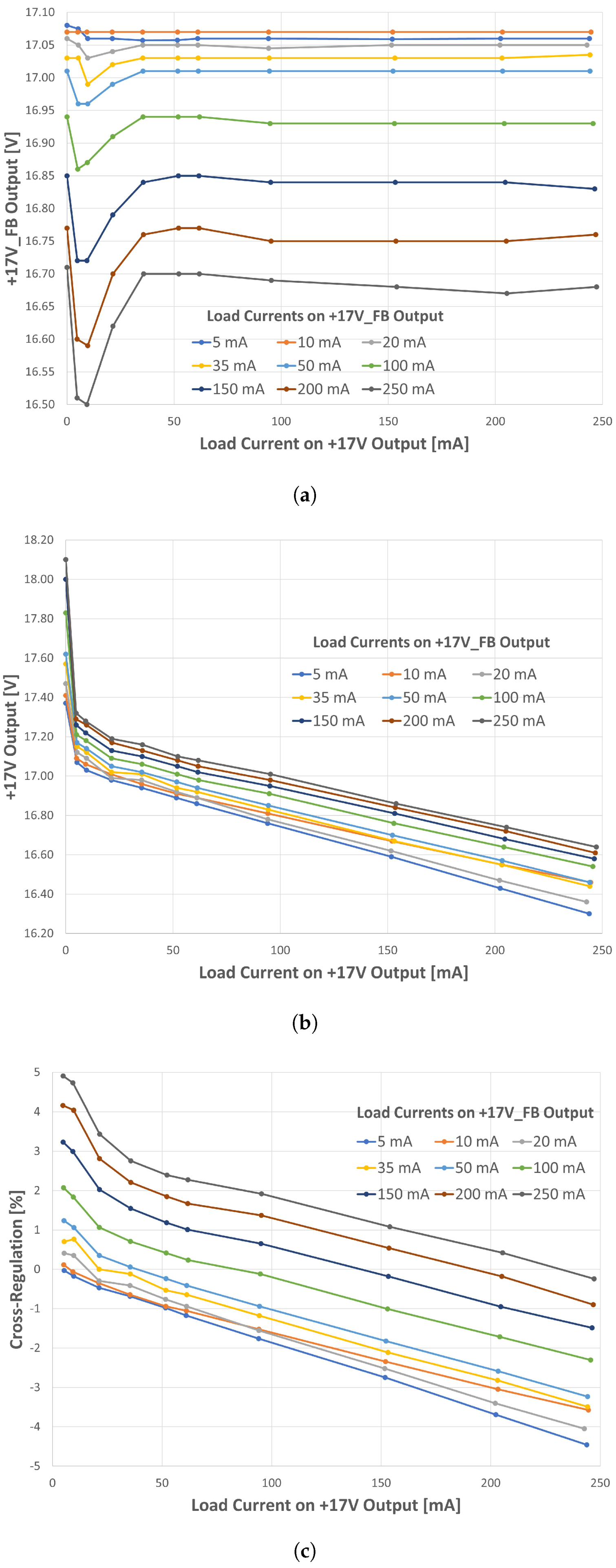
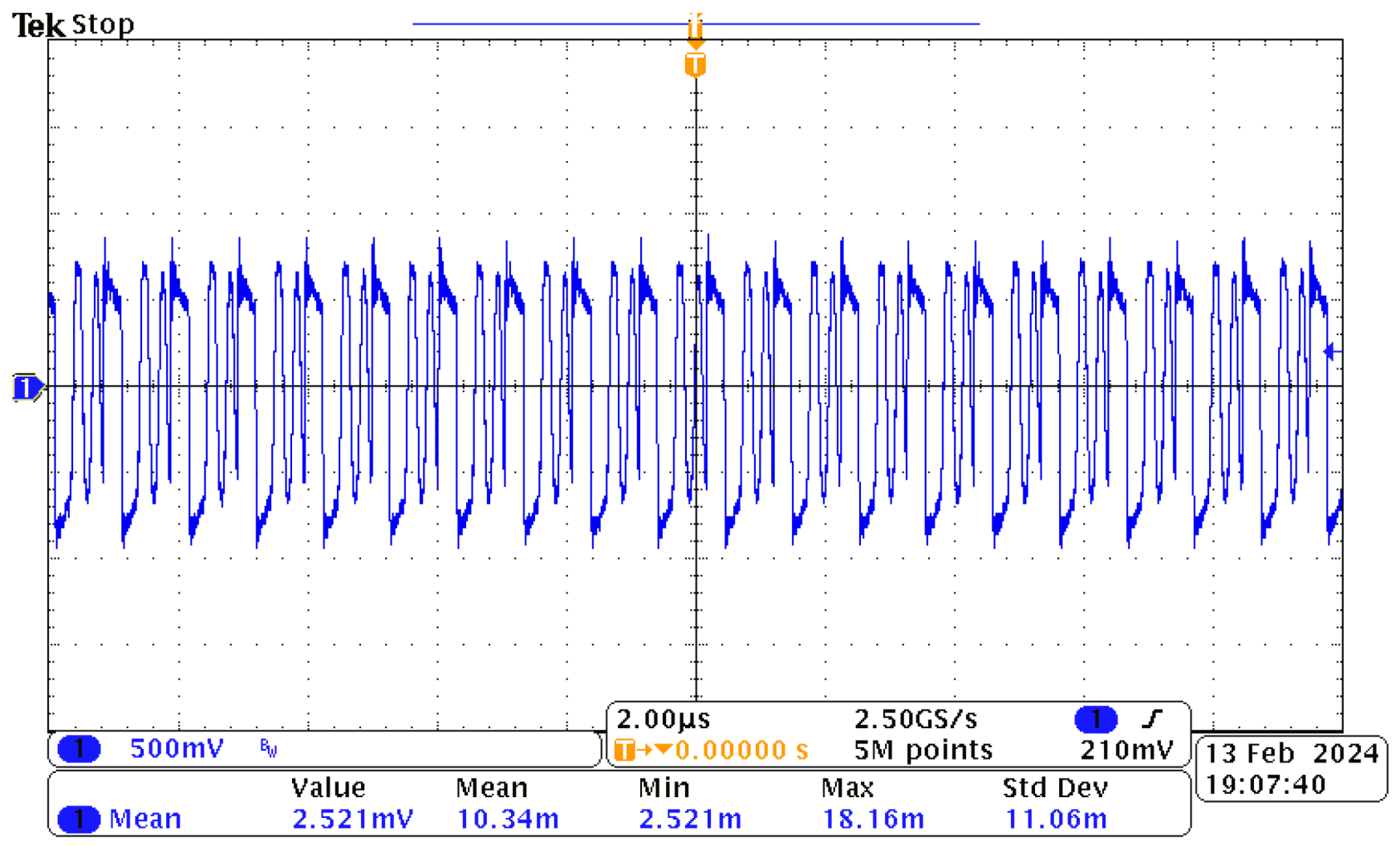
3. Experimental Section

The model outlined in Section 2 is assessed in this section by means of a prototype converter, providing double output at 17 V. The circuit schematic is depicted in Figure 4: a dual-positive output is obtained by a multi-winding transformer. One of the outputs, 17 V_FB, is regulated by means of a PMIC, whereas the other is left unregulated and is connected to the first one via a capacitor across the transformer secondary windings. A list of the main components utilized is reported in Table 1.
The selected transformer features a base winding inductance of 14.7 μ H, a typical leakage winding inductance of 210 nH, and a maximum winding DC resistance of 344 m Ω . Under full load conditions, when both outputs provide +17 V at 250 mA, and the input voltage is +15 V, the primary DC current stabilizes at 0.72 A. To adhere to the specified maximum DC current rating of 0.55 A for each winding, two primary side windings are connected in parallel. This configuration ensures a maximum of 0.36 A on each winding, maintaining compliance with the winding DC current rating. The top and bottom sides of the experimental prototype are shown in Figure 5. Figure 5c assesses that the transformer temperature settles around 58.5 °C under full current load conditions.
Since two windings in parallel are used to drive the input of the transformer, its saturation current results to be 1.62 A. Consequently, an LM51581 from Texas Instruments was selected to close the loop and regulate the +17 V_FB output. This PMIC features a 1.63 A integrated power switch with a voltage rating of up to 85 V. The switching frequency was set close to 1 MHz to match the transformer’s maximum operating frequency. To limit the voltage on the drain of the LM51581’s integrated power switch within safe limits, a TVS diode clamp was implemented. Consequently, a TPSMP24AHM3_A/H TVS diode ensured that a maximum voltage smaller than 50 V was applied to the drain during switching intervals. Additionally, V2PM10LHM3/H Schottky diodes, boasting a rating of 100 V, 2 A, and a peak forward surge current of 50 A, were employed for both the clamping diode, D S N , and the rectifying diodes, D O 1 and D O 2 . Finally, the input, output, and balancing capacitors were 22 μ F, 25 V, and XR5 ceramic capacitors. A total capacitance of 88 μ F, achieved by connecting four capacitors in parallel, was placed on each output and on the input. Additionally, to filter out high-frequency spikes, two 100 nF capacitors were placed close to the input. The main circuit parameters are summarized in Table 2.
This circuit with the parameters values discussed above and without the balancing capacitor C C exhibits a cross-regulation error that can exceed 20%, as shown in Figure 6.
The balancing capacitor C C mitigates this effect provided that it is chosen large enough to ensure that the resonance frequency of the series equivalent circuit comprising the leakage inductances L k 1 , L k 2 and the balancing capacitor C C is significantly smaller than the switching frequency, as stated in Equation (1) in Section 2. This is necessary to enable the series circuit to operate as a capacitive impedance, thereby providing a low-impedance current path for forwarding the balancing current. Accordingly, a C C capacitance value of 22 μ F was used for establishing a frequency of approximately 74 kHz in the worst-case unbalanced scenario, corresponding to less than 1/10 of the switching frequency. The voltage rating of the capacitor was chosen to match the output voltages. In this case study, we used capacitors with the same voltage ratings for both the outputs and C C .
It should be noted that for the circuit to operate properly, a minimum load must always be provided on the regulated output. Otherwise, the PMIC exhibits a random switching behavior. Consequently, no current is forced to flow through the balancing C C capacitor during the no-switching times, which invalidates the proposed model, as the unregulated output can no longer be balanced. Accordingly, the prototype tests are carried out with a minimum load of 5 mA applied on the regulated output, equivalent to the 2% of its maximum capability.
If both circuit outputs are loaded with the same current, the output voltages are balanced, as expected. The observed voltage difference between the +17 V and +17 V_FB outputs, as depicted in Figure 7, remains within a very small window, specifically between 0.059 % and 0.294 % .
On the contrary, if the output currents are unbalanced, a small cross-regulation is observed, as shown in Figure 8c. The +17 V_FB voltage is regulated by the feedback loop of the PMIC LM51581 and remains constant for different load currents, except for some small drift, as shown in Figure 8a. In contrast, the voltage on the unregulated output decreases linearly with increasing output currents, as depicted in Figure 8b. To evaluate the cross-regulation regardless of the DC error on the regulated +17 V_FB output, it is useful to plot the offset between the two outputs, normalized to the voltage on the regulated output, as shown in Figure 8c. It is evident that the offset changes linearly with the load, according to the behavior depicted in Figure 8b. In particular, it becomes positive when the current on the unbalanced output is smaller than that on the regulated output, and vice versa. Notably, when the output currents are equal, the offset settles close to 0% for the different load points, as previously described in Figure 7.
In Section 2, the average voltage drop across the balancing capacitor C C was derived to be zero in a steady state. Experimentally, its voltage drop was measured with a 100 mA load on the regulated output and 50 mA on the unregulated one, and the acquired scope waveform is shown in Figure 9. The measured average voltage is smaller than 3 mV, which is negligible compared to the measured voltage offset of 210 mV observed in the results presented in Figure 8.
Accordingly, given that the C C capacitor keeps the circuital nodes (as depicted in Figure 1) at the same voltage, the offset observed between outputs in the presence of unbalanced loads can be directly related to the difference between the forward voltage drops of the output rectifying diodes, in the specific operating conditions (Equation (28)).
The circuit was simulated for the same load currents used for the experimental tests reported in Figure 8, solely considering output rectifying and snubber diodes, along with magnetizing and leakage inductances. The primary switch is the internal switch of the LM51581 PMIC, and was modeled as an ideal switch with a series resistance R D S , o n of 150 m Ω . A linearized model was considered for the diodes D 1 , D 2 , and D S N with a forward voltage drop of 0.6 V and a series resistance of 500 m Ω ; An ESR of 5 m Ω was considered for each 22 μ F capacitor. The simulation was carried out in an open loop with fixed duty cycles that were adjusted on the basis of the load conditions to achieve the desired output voltage.
The results are shown in Figure 10, where the dashed lines representing the simulation results are compared with the continuous lines representing the experimental points in Figure 8c. It can be observed that the simulation results are quite close with the measurements, which confirms the accuracy of the developed model.

4. Conclusions

This study introduces an original analytical framework to model a dual-output flyback converter with capacitive coupling to address the challenge of improving cross-regulation. The proposed model demonstrates that the voltage across the balancing capacitor can be considered null if its capacitance is properly chosen. Under these conditions, the cross-regulation directly relates to the different voltage drops of output diodes when different currents are flowing through them.
A prototype for a dual-output flyback was built, with only one output regulated and the other connected to the first by means of a capacitor across the secondary windings of the transformer. Measurements for the output voltages were carried out under various load conditions.
Comparison of the measured results with the simulated ones demonstrated a tight correlation. This assessed the validity of the proposed model and the conclusions drawn regarding the balancing mechanism and the factors affecting the residual cross-regulation.

Author Contributions

Conceptualization, P.G.; methodology, P.G.; software, P.G.; validation, P.G. and L.S.; formal analysis, P.G.; investigation, P.G.; resources, P.G. and L.S.; data curation, P.G. and L.S.; writing—original draft preparation, P.G. and L.S.; writing—review and editing, P.G. and L.S.; visualization, P.G.; supervision, P.G. and L.S.; funding acquisition, P.G. All authors have read and agreed to the published version of the manuscript.

Funding

This research received no external funding.

Data Availability Statement

Data are contained within the article.

Conflicts of Interest

The authors declare no conflicts of interest.

References

  1. Schlesinger, K. Magnetic Deflection of Kinescopes. Proc. IRE 1947, 35, 813–821. [Google Scholar] [CrossRef]
  2. Dimitrov, B.; Krishna, M.; Cruden, A.; Sharkh, S.; Elkhateb, A. Analysis, Design, and Experimental Validation of a Primary Side Current-Sensing Flyback Converter for Use in a Battery Management System. Electronics 2018, 7, 43. [Google Scholar] [CrossRef]
  3. Yang, C.; Xie, F.; Chen, Y.; Xiao, W.; Zhang, B. Modeling and Analysis of the Fractional-Order Flyback Converter in Continuous Conduction Mode by Caputo Fractional Calculus. Electronics 2020, 9, 1544. [Google Scholar] [CrossRef]
  4. Shi, F.; Song, D. A Novel High-Efficiency Double-Input Bidirectional DC/DC Converter for Battery Cell-Voltage Equalizer with Flyback Transformer. Electronics 2019, 8, 1426. [Google Scholar] [CrossRef]
  5. Xue, L.; Zhang, J. Highly Efficient Secondary-Resonant Active Clamp Flyback Converter. IEEE Trans. Ind. Electron. 2018, 65, 1235–1243. [Google Scholar] [CrossRef]
  6. Gao, S.; Song, H.; Wang, Y.; Xu, R.; Xu, D. A Secondary-Resonance MHz Active-Clamp Flyback Converter with Partial Power Processing. IEEE Trans. Ind. Appl. 2022, 58, 7988–7997. [Google Scholar] [CrossRef]
  7. Granello, P.; Soeiro, T.B.; van der Blij, N.H.; Bauer, P. Revisiting the Partial Power Processing Concept: Case Study of a 5-kW 99.11% Efficient Flyback Converter-Based Battery Charger. IEEE Trans. Transp. Electrif. 2022, 8, 3934–3945. [Google Scholar] [CrossRef]
  8. Özen, S.H.; Doğru, U.E.; Yaşar, R.Ö.; Akboy, E. Multiple Output Application of Quasi-Resonant Flybacks on TV Applications. In Proceedings of the 2023 14th International Conference on Electrical and Electronics Engineering (ELECO), Bursa, Turkey, 30 November–2 December 2023; pp. 1–6. [Google Scholar] [CrossRef]
  9. Duzgun, R.; Parlak, M.; Yilmazlar, I. Design of Multiple-Output Flyback Converter with Independently Controlled Outputs for TV Power Supply. In Proceedings of the 2023 18th Conference on Electrical Machines, Drives and Power Systems (ELMA), Varna, Bulgaria, 29 June–1 July 2023; pp. 1–4. [Google Scholar] [CrossRef]
  10. Sarkar, A.; Vankayalapati, B.T.; Anand, S. GaN-Based Multiple Output Flyback Converter with Independently Controlled Outputs. IEEE Trans. Ind. Electron. 2022, 69, 2565–2576. [Google Scholar] [CrossRef]
  11. Kim, J.-K.; Lee, J.-B.; Moon, G.-W. Zero-Voltage Switching Multioutput Flyback Converter with Integrated Auxiliary Buck Converter. IEEE Trans. Power Electron. 2014, 29, 3001–3010. [Google Scholar] [CrossRef]
  12. Ji, C.; Smith, K.M.; Smedley, K.M. Cross regulation in flyback converters: Solutions. In Proceedings of the IECON’99. Conference Proceedings. 25th Annual Conference of the IEEE Industrial Electronics Society (Cat. No.99CH37029), San Jose, CA, USA, 29 November–3 December 1999; Volume 1, pp. 174–179. [Google Scholar] [CrossRef]
  13. Ji, C.; Smith, M.; Smedley, K.M.; King, K. Cross regulation in flyback converters: Analytic model and solution. IEEE Trans. Power Electron. 2001, 16, 231–239. [Google Scholar] [CrossRef]
  14. Maksimovic, D.; Erickson, R.W.; Griesbach, C. Modeling of cross-regulation in converters containing coupled inductors. IEEE Trans. Power Electron. 2000, 15, 607–615. [Google Scholar] [CrossRef]
  15. Hu, Y.; Zhang, J.; Chen, W.; Wen, C. Mathematical modeling of cross-regulation problem in flyback converters. In Proceedings of the 2001 IEEE 32nd Annual Power Electronics Specialists Conference (IEEE Cat. No.01CH37230), Vancouver, BC, Canada, 17–21 June 2001; Volume 4, pp. 2072–2077. [Google Scholar] [CrossRef]
  16. Guo, X.; Wu, S.; Zhang, Y.; Dou, C.; Chi, Y. Optimal Design of High Frequency Transformer for High Power Density Flyback Converter. IEEE Trans. Circuits Syst. II Express Briefs 2022, 69, 4399–4403. [Google Scholar] [CrossRef]
  17. Kim, J.-W.; Ha, J.-I. Dual voltage regulations of single switch flyback converter using variable switching frequency. In Proceedings of the 2016 IEEE Applied Power Electronics Conference and Exposition (APEC), Long Beach, CA, USA, 20–24 March 2016; pp. 1398–1402. [Google Scholar] [CrossRef]
  18. Jung, J.-H.; Ahmed, S. Flyback converter with novel active clamp control and secondary side post regulator for low standby power consumption under high-efficiency operation. IET Power Electron. 2011, 4, 1058–1067. [Google Scholar] [CrossRef]
  19. Tahan, M.; Bamgboje, D.; Hu, T. Flyback-Based Multiple Output dc-dc Converter with Independent Voltage Regulation. In Proceedings of the 2018 9th IEEE International Symposium on Power Electronics for Distributed Generation Systems (PEDG), Charlotte, NC, USA, 25–28 June 2018; pp. 1–8. [Google Scholar] [CrossRef]
  20. Kolincio, M.; Chrzan, P.J.; Musznicki, P. Multitransformer Primary-Side Regulated Flyback Converter for Supplying Isolated IGBT and MOSFET Drivers. IEEE Trans. Ind. Electron. 2020, 67, 1005–1012. [Google Scholar] [CrossRef]
  21. Wen, C.-C.; Chen, C.-L. Magamp application and limitation for multiwinding flyback converter. IEE Proc. Electr. Power Appl. 2005, 152, 517–525. [Google Scholar] [CrossRef]
  22. Chalermyanont, K.; Sangampai, P.; Prasertsit, A.; Theinmontri, S. High Frequency Transformer Designs for Improving Cross Regulation in Multiple-Output Flyback Converters. In Proceedings of the 2007 7th International Conference on Power Electronics and Drive Systems, Bangkok, Thailand, 27–30 November 2007; pp. 53–56. [Google Scholar] [CrossRef]
  23. Xu, Y.; An, S.; An, S.; Wu, Y.; Wu, Q.; Zhang, Q. A High-Efficiency Multiple Output Flyback Converter Based on Variable Width Winding Planar Magnetics. In Proceedings of the 2023 IEEE 14th International Symposium on Power Electronics for Distributed Generation Systems (PEDG), Shanghai, China, 9–12 June 2023; pp. 773–779. [Google Scholar] [CrossRef]
  24. Guo, X.; Luan, F.; Liu, J.; Liu, M. Analysis and improvement of cross-regulation effect in the primary side-regulated multi-output flyback converter. Int. J. Circ. Theor. Appl. 2017, 45, 1299–1312. [Google Scholar] [CrossRef]
  25. Zhu, G.; Liu, X.; Qin, Z.; Zhang, Q.; Liu, S.; Fang, W. Research on Low Cross Regulation Multiple High Voltage Output Converter Based on Magnetic Decoupling. In Proceedings of the 2023 IEEE 2nd International Power Electronics and Application Symposium (PEAS), Guangzhou, China, 10–13 November 2023; pp. 1222–1227. [Google Scholar] [CrossRef]
  26. Lee, M.; Lio, J.; Chen, D.Y.; Chen, Y.; Wu, Y. Small-signal modeling of multiple-output flyback converters in continuous conduction mode with weighted feedback. IEEE Trans. Ind. Electron. 1998, 45, 236–248. [Google Scholar] [CrossRef]
  27. Leng, C.-M.; Chiu, H.-J. Three-Output Flyback Converter with Synchronous Rectification for Improving Cross-Regulation and Efficiency. Electronics 2021, 10, 430. [Google Scholar] [CrossRef]
  28. Mullett, C.; Cathell, F. Improving the Regulation of Multi-Output Flyback Converters. In Proceedings of the 2009 Twenty-Fourth Annual IEEE Applied Power Electronics Conference and Exposition, Washington, DC, USA, 15–19 February 2009; pp. 1923–1926. [Google Scholar] [CrossRef]
  29. Halder, T. An elimination technique of cross regulations in the flyback converters. In Proceedings of the 2014 IEEE 6th India International Conference on Power Electronics (IICPE), Kurukshetra, India, 8–10 December 2014; pp. 1–6. [Google Scholar] [CrossRef]
  30. Wilson, T.G., Jr. Cross regulation in a two-output DC-to-DC converter with application to testing of energy-storage transformers. In Proceedings of the 1978 IEEE Power Electronics Specialists Conference, Syracuse, NY, USA, 13–15 June 1978; pp. 124–134. [Google Scholar] [CrossRef]
Figure 1. Flyback converter with C C balancing capacitor.
Electronics 13 03503 g001
Figure 2. Modeling of voltage and current waveforms in DCM.
Electronics 13 03503 g002
Figure 3. Equivalent circuits during different subintervals. (a) Subinterval 1; (b) Subinterval 2; (c) Subinterval 3; (d) Subinterval 4.
Electronics 13 03503 g003
Figure 4. Prototype circuital schematic with a single regulated output.
Electronics 13 03503 g004
Figure 5. Experimental prototype. (a) Top side; (b) Bottom side; (c) Thermal image under full load conditions.
Electronics 13 03503 g005
Figure 6. Output voltage cross-regulation without balancing capacitor.
Electronics 13 03503 g006
Figure 7. Difference in output voltages with balanced load currents.
Electronics 13 03503 g007
Figure 8. Measurements with unbalanced output current loads. (a) Voltage on regulated output (+17 V_FB); (b) Voltage on unregulated output (+17 V); (c) Cross-regulation error.
Electronics 13 03503 g008
Figure 9. Measured voltage across balancing C C capacitor.
Electronics 13 03503 g009
Figure 10. Comparison between measured and simulated results.
Electronics 13 03503 g010
Table 1. Circuit components.
ComponentManufacturerValue
T1Würth Elektronik749196121
U1Texas InstrumentsLM51581
D3, D4, DSNVishayV2PM10LHM3/H
TVSVishayTPSMP24AHM3_A/H
C C , C1, C5, C6SamsungCL21A226MAYNNNE
Table 2. Main circuit parameters.
ParameterValueParameterValue
f S 1 MHz L B A S E 14.7 μ H
V I N 15 V L k 1 210 nH
V O U T _ F B 17 V L k 2 210 nH
Disclaimer/Publisher’s Note: The statements, opinions and data contained in all publications are solely those of the individual author(s) and contributor(s) and not of MDPI and/or the editor(s). MDPI and/or the editor(s) disclaim responsibility for any injury to people or property resulting from any ideas, methods, instructions or products referred to in the content.

