Article

Development of a Wafer Defect Pattern Classifier Using Polar Coordinate System Transformed Inputs and Convolutional Neural Networks

School of Information, Communications and Electronics Engineering, The Catholic University of Korea, Bucheon 14662, Republic of Korea
*
Author to whom correspondence should be addressed.
Electronics 2024, 13(7), 1360; https://doi.org/10.3390/electronics13071360
Submission received: 12 March 2024 / Revised: 1 April 2024 / Accepted: 2 April 2024 / Published: 4 April 2024
(This article belongs to the Special Issue Feature Papers in Semiconductor Devices)

Abstract

:
Defect pattern analysis of wafer bin maps (WBMs) is an important means of identifying process problems. Recently, automated analysis methods using machine learning or deep learning have been studied as alternatives to manual classification by engineers. In this paper, we propose a method to improve the feature extraction performance of defect patterns by transforming the polar coordinate system instead of the existing WBM image input. To reduce the variability of the location representation, defect patterns in the Cartesian coordinate system, where the location of the distributed defect die is not constant, were converted to a polar coordinate system. The CNN classifier, which uses polar coordinate transformed input, achieved a classification accuracy of 91.3%, which is 4.8% better than the existing WBM image-based CNN classifier. Additionally, a tree-structured classifier model that sequentially connects binary classifiers achieved a classification accuracy of 94%. The method proposed in this paper is also applicable to the defect pattern classification of WBMs consisting of different die sizes than the training data. Finally, the paper proposes an automated pattern classification method that uses individual classifiers to learn defect types and then applies ensemble techniques for multiple defect pattern classification. This method is expected to reduce labor, time, and cost and enable objective labeling instead of relying on subjective judgments of engineers.

1. Introduction

Integrated circuit (IC) chips are manufactured by hundreds of steps of continuous and complex chemical, optical, and mechanical processing on a semiconductor wafer. A single wafer may contain tens or hundreds of chips (or dies) that are manufactured to have uniform performance. Semiconductor companies are continuously developing miniaturization processes to produce more dies from a single wafer, reducing costs and enhancing integration. This complex semiconductor manufacturing process and miniaturization process make the chips on the wafer susceptible to various types of defects. To detect the defects during the manufacturing process and analyze their causes, the wafer test steps are essential [1]. A typical wafer level test method is electrical die sorting (EDS), which is used to test the electrical characteristics of the chip. EDS tests focus on sorting chips or wafers through AC and DC parameter tests. Additionally, EDS can provide information on fabrication yield and chip functionality. Each die is assigned a bin code or bin code number based on the test results to identify the cause of the defect. Through this process, the defective dies on the wafer are visually represented according to the cause of the defect, forming a wafer image called a wafer bin map (WBM) as shown in Figure 1. Each die is normally represented by a binary logical value of ‘0’ or ‘1’ when a WBM determines only whether a die is failed or not. When the test results require a more detailed distinction between defect types, predetermined symbols or values are assigned to represent them. These values can be used to classify the type of wafer defect as a two-dimensional pattern, which can be categorized into typical pattern types such as ‘Center’, ‘Donut’, ‘Edge-Loc’, ‘Edge-Ring’, ‘Loc’, ‘Near-Full’, ‘Random’, ‘Scratch’, or ‘none’, depending on the spatial characteristics of the defect pattern [2,3,4].
The ultimate goal of this research is to develop a system that can automatically diagnose process problems quickly and accurately using WBM data acquired in the semiconductor manufacturing process. For this, objective of this paper is to develop a system that classifies the type of WBM pattern based on data from eight types of defect patterns. Conventionally, experienced failure analysis engineers view WBM images and manually classify failure patterns. However, manual classification methods are inefficient in terms of time and cost and rely on subjective judgment of engineers, which limits the repeatability of measurements. These issues significantly reduce the accuracy and efficiency of WBM analysis and defect cause identification. For this reason, many semiconductor companies are continuously researching to automate defect pattern classification using machine learning and deep learning techniques. Existing studies show that efforts have been made to improve the classification accuracy of defect patterns by using WBM images as training data for CNNs [5,6,7]. Upon analyzing each defect pattern on the WBM image used here, we can see that there are positional and geometric features in the distribution of defect dies for each defect pattern class. Figure 2a shows the defect pattern where the defect die group is distributed in the center of the WBM, which belongs to the ‘Center’ class. The ‘Donut’ class is defined by the defect pattern where the defect die is distributed in a donut shape. The ‘Edge-Ring’ pattern is characterized by the distribution of defect dies along the edge of the WBM. For patterns such as ‘Center’, ‘Donut’, and ‘Edge-Ring’, the images belonging to these classes exhibit almost identical defect die distributions based on the in-plane position of each wafer. However, as depicted in Figure 2b, in the case of ‘Edge-Loc’, ‘Loc’, and ‘Scratch’ patterns, the defect die clusters do not appear at a constant location. Rather, the spatial location of the defect die clusters varies from image to image. Therefore, even if they belong to the same class, the location information of the defect dies in the space represented by the Cartesian coordinate system makes the images look quite different depending on their distribution. As a result, it is necessary to learn how to transform the WBM image data to better represent their positional features, rather than using the WBM image itself as the input of the classifier as in existing methods.
In this paper, we construct six models, including a comparison model, and evaluate their performance based on input data conversion, pre-processing method, and classifier structure. Section 4 describes the specific configuration of these models. We evaluated and compared the performance of the proposed method using the real-world WM-811K dataset through training and testing on 26 × 26-sized WBMs. Experiments were conducted to classify the defect patterns of different-sized WBMs from the trained data to confirm the model’s general applicability. First, the defect die information on the WBM is converted to the polar coordinate system to enhance the characteristics of the distribution of defect dies by wafer defect class, rather than using the WBM image as input. To clarify, instead of using Cartesian coordinates (x, y) to express position information, the distance information was expressed as r, and the rotation information was expressed as θ, centered on the center of the circular wafer, so that the position characteristics of the defect pattern could be easily defined. If the transformed information from the polar coordinates is used, the amount of information from the points corresponding to the defective dies will be quite small compared to the entire space consisting of the radii and angles. To solve this problem, the space of the polar coordinate system is divided into a certain range, and the number of defective dies belonging to that area is measured and pre-processed to be used as input. In summary, the location information is resolved to the necessary level for defect pattern classification. The degree of defect at that location is expressed by the number of defect dies, allowing for robust classification of various types of WBM. Three different classification models were used for classification and their performance was compared. A single CNN and a binary tree-structured classifier were used for single failure pattern classification, while a CNN-based ensemble classifier was used for mixed defect pattern classification. The binary classifier-based tree structure classification model trained on polar coordinate system data is a sequentially connected structure of binary classifiers to classify defect patterns with relatively clear distribution compared to other defect patterns first. In this way, we aimed to improve the classification accuracy compared to the existing model that classifies eight patterns at a time. Finally, we designed individual classifiers for each class to classify mixed defect patterns. These classifiers were trained on polar coordinate data, and an ensemble defect pattern classification model was presented. Based on the engineer’s judgment, we found that many WBMs contain multiple defect patterns rather than single defect patterns, although the dataset we used does not have accurate labeling information for multiple defect patterns.
The paper presents three novel contributions. Firstly, the use of a polar coordinate system transformation enhances the ability to classify patterns that are difficult to define as similar defect patterns in the conventional Cartesian coordinate system plane. Second, we showed that WBMs with different die sizes or wafer dimensions can be classified by the proposed system without additional training. Finally, we demonstrated the possibility of identifying WBMs with mixed defect patterns to comprehend the limitations of the original dataset, which was labeled with only a single failure pattern. The proposed method in this paper clarifies the location information of the defect pattern through the polar coordinate space representation, rather than relying on the location and shape information of the defect pattern represented in the WBM image or Cartesian coordinate system. Additionally, we were able to evaluate performance differences based on the pre-processing method and classifier model. Furthermore, we verified the labeling results of the WM-811K dataset using the mixed defect pattern classification model. Most previous papers using this dataset approached it as a pattern recognition problem to improve classification accuracy. However, in this paper, we were able to identify the limitations of the labeling defined in the dataset through mixed defect pattern classification to provide information necessary for actual semiconductor manufacturing.

2. Related Work

2.1. Single-Failure Pattern Classification

With the growth of the semiconductor industry, many techniques have been studied to effectively classify defect patterns on wafers. Li and Huang proposed a method that combines self-organizing maps (SOMs) and support vector machines (SVMs) for binary bin map classification [5]. They emphasized that the combination of unsupervised SOM-based clustering and supervised SVM-based classification methods has computational advantages for solving large-scale problems, and the classification performance is better than the existing BP. However, it is to be considered that the optimal number of clusters for classifying defect types or defect patterns varies depending on the type of data. Wu et al. extracted rotation- and scale-invariant wafer-specific features based on geometry from wafer map images and used them for failure pattern classification of wafers with different die sizes [8]. The authors applied the features to large-scale real-world wafer map data and demonstrated their efficient processing in wafer map failure pattern recognition (WMFPR) and wafer map similarity ranking (WMSR). Furthermore, Piao et al. [9] utilized the radon transform and interpolated projection to generate max, min, average, and standard deviation values and classified failure patterns using a decision tree. While their proposed method demonstrated superior failure pattern recognition performance compared to many existing algorithms, it was found to be insufficient in describing the spatial information of defects on the wafer when multiple failure patterns exist, thus limiting its overall performance. Several methods have been studied to classify single-defect patterns. Conventional classification methods, such as SVM, were applied in the beginning [10]. More recently, researchers have employed deep learning methods, mostly based on convolutional neural network (CNN) models [5,6,7]. CNNs possess translational invariance, which ensures that the absolute position of any image does not affect the classification performance of the model. Well-known models include ResNet and VGG16, and several studies have shown that these CNNs have strong image classification performance [11,12]. Nakazawa and Kulkarni [5] generated 28,600 synthetic wafer maps containing 22 different defect patterns and used them as training data for a CNN to perform defect pattern classification, resulting in a retrieval error rate of 3.7%. Wang and Tsai [13] also attempted classification using the MobileNet V2 algorithm to reduce the computational complexity compared to a typical CNN. Koo and Ko [14] used vectors encoding topological features as input to CNNs based on topological data analysis (TDA). Using TDA is a very different approach than traditional methods, and it allowed them to outperform traditional CNN-based models in experiments with small amounts of data and imbalanced data. Shin and Yoo [15] applied lightweight models such as EfficientNetV2, ShuffleNetV2, and MobileNetV3 to wafer map classification and compared them in terms of classification performance, hardware resource utilization, and execution time. They showed that fast inference is possible without high-performance hardware, making their proposed method applicable to real-world manufacturing. Wang et al. [16] proposed a two-stage classifier model with self-supervised pre-training using unlabeled WBMs followed by a few-shot fine tuning. They showed that it can classify effectively even with a small amount of labeled data. However, the proposed model is a single-defect classification model, but since real WBMs often have multiple defects, further research is needed to develop a multi-defect classification model.
While the selection of an appropriate pattern classifier is very important, for datasets with unbalanced data per class, such as semiconductor defect pattern classification, additional operations such as data augmentation are often required in the data pre-processing stage to improve classification performance. Nakazawa et al. and Shim et al. balanced the data by using a small amount of real wafer data and additional synthesized data [5,17]. To address the imbalance in the dataset, Theodoros Tziolas et al. [18] independently processed each class in proportion to the number of samples. Abu Ebayyeh et al. [19] augmented the data in a balanced manner using a deep convolutional generative adversarial network (DCGAN) and then utilized a capsule network for classification. Park and You [20] also used a DCGAN-based data augmentation method to improve the performance of a defect pattern classifier with extremely imbalanced data. They also presented a metric called polymorphic generative index (PGI) to quantitatively evaluate the performance of the augmented model intuitively, although with some performance limitations.
Given that semiconductor mass production systems require continuous process optimization and new process technologies are being introduced, analysis methods that only consider previously defined defect patterns may not be sufficient. Additionally, manually labeling defect patterns for products with varying die sizes is a laborious task. Considering this, research has been conducted using unsupervised learning methods, which are useful for handling large amounts of unlabeled data. Shon et al. presented a methodology to train a convolution-based variational autoencoder (CVAE) in an unsupervised manner [21], and Qiao Xu et al. used unlabeled data to learn common defect patterns using an unsupervised method [22]. However, only a few studies have used pure unsupervised learning. Recently, many studies have utilized the concept of semisupervised learning, which applies supervised learning to a small amount of labeled data and unsupervised learning to a large amount of unlabeled data. Niu et al. proposed a semisupervised fault detection method using GANs [23]. Li et al. also employed semisupervised learning by training a predictive model with labeled data and sending suspicious samples to an unsupervised learning algorithm [24]. These works have stimulated research on defect wafer image classification, leading to the problem of classifying mixed defect patterns, which will be discussed in the next section.

2.2. Mixed Failure Pattern Classification

In semiconductor chip mass production, it is common for multiple defect patterns to appear on a wafer simultaneously. However, there is limited research on the classification of mixed defect patterns compared to single defect patterns. The most common methodology for classifying mixed defect patterns is to separate them into multiple single patterns on a wafer map. Various methods can be used to combine multiple defect patterns into a single pattern, including hierarchical clustering, spectral clustering, support vector clustering, and density-based spatial clustering of applications with noise (DBSCAN). Among them, Wang et al. [25] showed that the single linkage method provides the best separation performance for unlinked mixed patterns. When dealing with mixed defect patterns, it is common for multiple patterns to be stuck together, making it difficult to separate them into a single pattern. Kim et al. [26] proposed a methodology that utilizes connectivity path filtering and an infinite warped mixture model (iWMM) to separate clusters of complex shapes. Remya et al. also attempted to classify mixed patterns by training several of them using ResNet50 [11].
In general, studies on defect pattern classification aim to separate outlier detection and defect pattern detection into independent steps. However, Jin et al. [27] presented a methodology that trains the DBSCAN algorithm using polar coordinate system data and performs both defect pattern and outlier removal simultaneously. After setting the appropriate parameters using DBSCAN, a set of defective dies that are successfully clustered is considered as a defect pattern. Dies that do not belong to the cluster are considered as outliers and removed. If multiple clusters of defect patterns are obtained from a single wafer map, they are classified as mixed patterns. The clusters extracted using this method can be referred to as mixed patterns. This approach proves useful when the algorithm parameters are adjusted based on the distribution of defect dies in each wafer map. However, this study only presents the classification results for Near-Full patterns. Therefore, it is unclear whether the same method is valid for the remaining pattern types, and further research is required.
Kyeong and Kim [28] proposed a methodology to solve the mixed-type defect pattern classification problem and the data imbalance problem by creating separate classifiers for each class using the ensemble method. In this study, a multi-pattern classifier to distinguish the presence and absence of the corresponding patterns for the four classification models was implemented by creating classifiers for four pattern classes (Scratch, Ring, Circle, and Zone). Liu and Tang [29] addressed the mixed-type defect pattern classification problem by transforming it into a single defect classification problem using a triplet CNN model instead of a binary CNN. They utilized a weakly supervised learning approach to acquire highly imbalanced defect data without additional manual labeling, which is beneficial for practical applications. Wang and Chen [30] proposed a noise-robust composite defect pattern classification model by separating mixed-type defect patterns into clusters using a method called tensor voting. Tensor voting is a perceptual grouping method used to obtain continuous smooth curves, junctions, and regions in two- or three-dimensional (2D/3D) space. The extracted patterns were recognized as 16 types of failure patterns on the basis of a simple decision tree, and the performance was better than the results of the combination of the existing clustering method and a CNN.
Furthermore, X-ray computed tomography has been recently utilized for defect analysis in various engineering fields [31,32]. If high-resolution 3D images of semiconductor chips can be acquired through this method, physical defect analysis will be possible. As described above, the models for classifying defect patterns in WBM are mainly based on CNNs and focus on developing CNN architectures and algorithms to improve the classification accuracy of defect patterns. However, these studies are mainly aimed at improving the pattern recognition accuracy based on the dataset without considering the error of the original data’s label. Therefore, it is necessary to verify the dataset in addition to developing classification algorithms to accurately determine the type of defective pattern and diagnose process problems quickly. In this paper, the training data were filtered to exclude data with label values that do not clearly express the characteristics of WBM due to subjective judgments of engineers or the label method that can only express a single-defect pattern. To enhance pattern classification accuracy, the WBM information was represented as a polar coordinate system. Additionally, the number of defective dies per block was used as input to improve defect classification performance. Further details are explained in the next section.

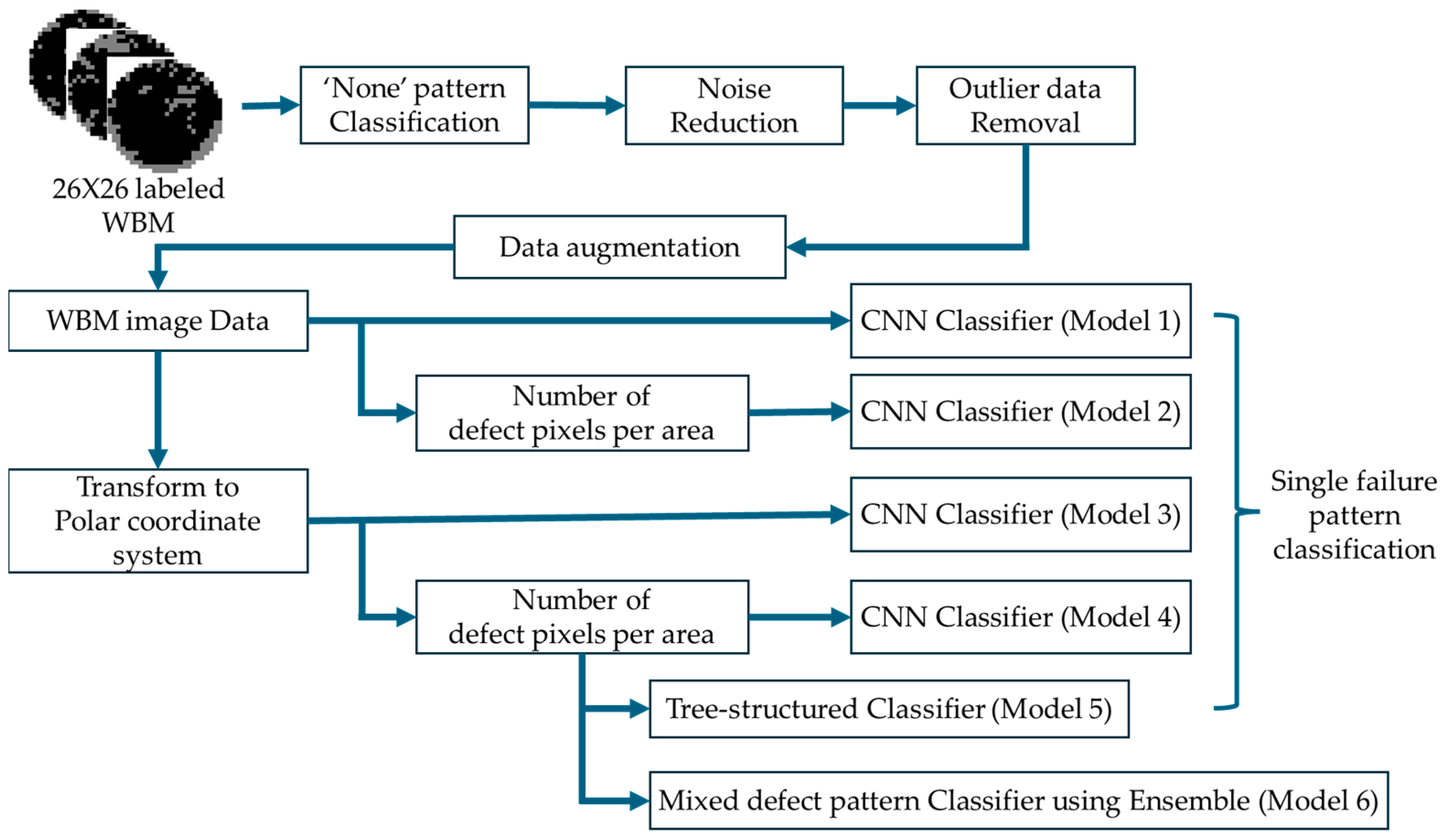
3. Materials and Methods
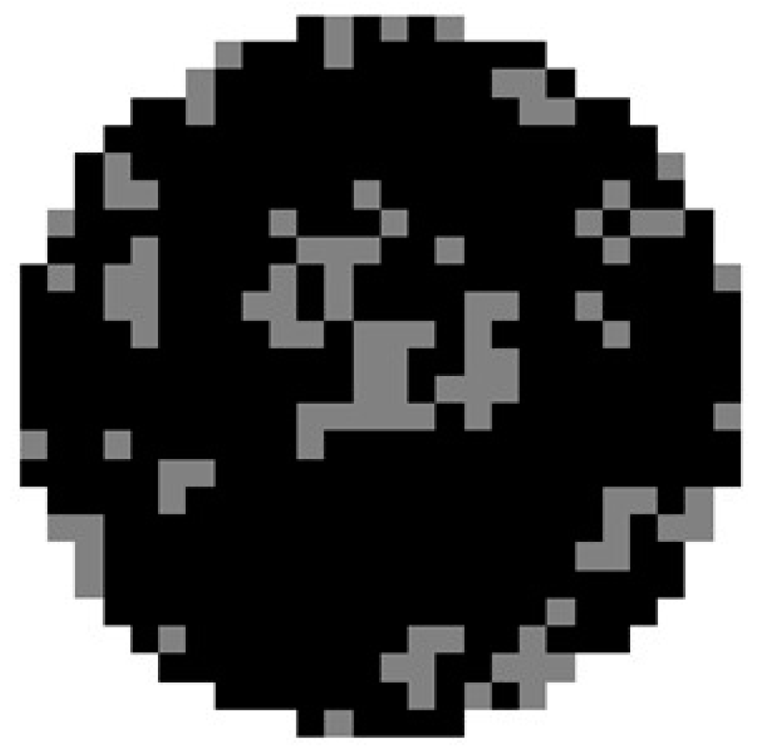
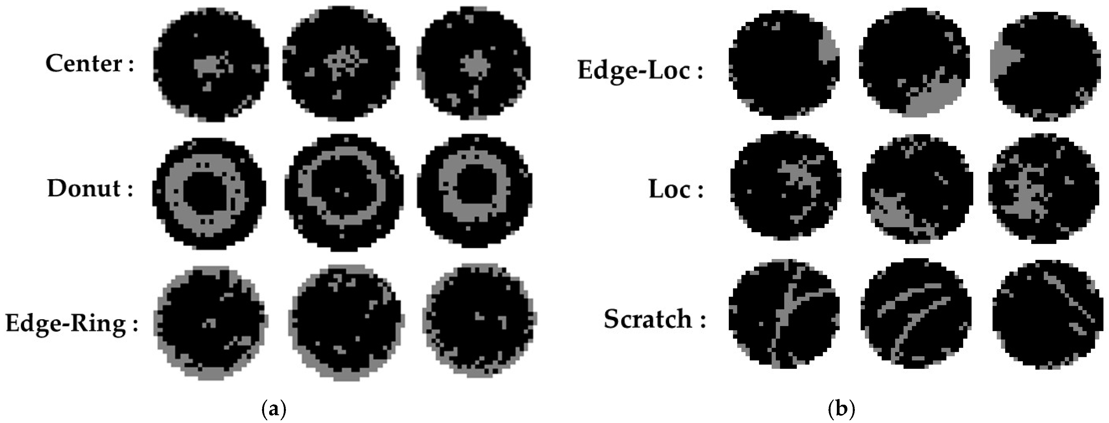
In this paper, we present a methodology for classifying wafer defect patterns using class-based defect distribution features. In this paper, instead of using image data as input for WBM defect pattern classification, we proposed a framework to enhance the spatial features of defect dies by converting the polar coordinate system to improve the classification accuracy and detect mixed defect patterns based on these data. Figure 3 illustrates the overall flowchart of the proposed process. In this paper, we use WM-811K, a real-world open dataset that is commonly used for WBM pattern classification, as the original data [8]. At first, we extract 26 × 26 images from different sizes of WBM images and store only labeled data separately. In WM-811K, each wafer is labeled with 9 types of defect patterns, including ‘none’ (no defect pattern) and 8 defect patterns. We employed SVM to identify the presence or absence of defect patterns. For the remaining 8 classes of defect pattern images, any defect die that exists randomly, regardless of the typical pattern of a specific defect, is considered as noise and removed. Data augmentation is then performed to compensate for the imbalance between the WBM data labeled by defect type.
The data generated by the WBM is divided into two types of inputs, and each type of input is fed into the classifier for evaluation of its performance. The first input has a structure in which the defective die and the normal die are divided into binary codes and the values are listed sequentially according to the (x, y) values in the Cartesian coordinate system. In other words, the WBM image is represented as a bitmap to provide WBM information to the CNN. To evaluate the pre-processing performance for the method that used WBM images as training data, we compared the classification performance of the model that trained the image data itself and the model that used the number of defect dies in the specified area as training data. The second method involves classifying defect patterns using data generated by a polar coordinate system-based conversion. First, the WBM data are denoised and augmented and then converted to polar coordinate system data. Each defect die on the WBM is assigned a polar coordinate system value consisting of the distance from the origin and the angle (r, θ) away from the baseline. At this point, the distance and angle are divided into specific ranges, and defect images within each range are extracted and used as training data for the CNN (the detailed description is presented in Section 3.2). Subsequently, we compared the classification performance of the CNN classifier trained using WBM image data with the CNN classifier trained using polar coordinate system data.
Next, we present a defect pattern classifier that applies polar coordinate data and a tree structure. The defect pattern classifier that applied the tree structure classified eight types of defect patterns through a binary classification model using the CNN algorithm. To enhance the accuracy of defect pattern classification, we first classified patterns with consistent defect distribution features of WBMs belonging to the class, as shown in Figure 2a, by placing them close to the root node. Later, patterns with high randomness of defect distribution were classified, as shown in Figure 2b.
We constructed a CNN-based ensemble model using polar coordinate system data to classify mixed defect patterns. A binary classification model was trained for each of the eight defect patterns (Center, Donut, Edge-Loc, Edge-Ring, Loc, Near-Full, Random, and Scratch) by re-labeling the polar coordinate system data into the corresponding defect pattern or other patterns. The models trained for each class were then ensembled to produce eight classification results. Additionally, a model capable of identifying two mixed defect patterns was presented.

3.1. Dataset

The dataset used in this paper, WM-811K, is open data consisting of WBMs of various die sizes collected from actual semiconductor manufacturing, with about 20% of the WBMs in the dataset labeled by domain experts [8]. Out of the 811,457 WBMs in WM-811K, 638,507 are unlabeled, and only 172,950 are labeled with ‘none’ and 8 types of defect patterns (Center, Donut, Edge-Loc, Edge-Ring, Loc, Near-Full, Random, Scratch). However, out of the 172,950 labeled data, only 25,519 (3.1%) are labeled with a defect pattern, while the remaining 147,431 are labeled as ‘none’. The WM-811K dataset includes 1266 wafers with varying die sizes, and the WBM contains 632 datasets with different die distributions on the wafer, depending on the wafer and die size.
To develop a robust defect pattern classifier by machine learning or deep learning, the data must be accurately labeled and a sufficient number of data must be acquired to learn the features of each defect pattern. As previously stated, the WM-811K dataset contains a relatively small number of labeled data, and the number of dies on the wafer and the area occupied by the die vary. Therefore, it is not appropriate to use the original data directly. To address this issue, a data selection process was applied in this paper, and we have taken 26 × 26 WBMs among various sizes of WBMs. Table 1 lists the number of data by defect type for the 26 × 26 WBMs. The data show a high number of ‘none’ pattern defects compared to other types, which is consistent with the overall imbalance in semiconductor production data. To solve this data imbalance problem, this paper uses a two-step classification method that first determines the presence or absence of defect patterns, and then classifies the defect types for WBMs containing defect patterns.
Upon reviewing the 26 × 26 WBM images, as shown in Figure 4, it is evident that the shape of the WBM is not always well matched to the defined label, or there are cases where two or more defect types are combined and only one label is labeled. Specifically, we observed numerous instances in the ‘Edge-Loc’, ‘Loc’, and ‘Scratch’ categories where pattern classification is subject to the engineer’s subjective evaluation. If the labeled results are not objective or if it is difficult to determine that the labeled WBM is representative of the pattern, it can be difficult to extract the spatial features of each class and become a major factor in reducing the classification accuracy if the training data of the classifier contain data that are not representative of the pattern. Therefore, we considered these images as outliers and removed them from the training data.
However, as shown in Table 1, there is only one ‘Donut’ pattern among the 26 × 26 size WBM data. Therefore, we artificially generated a pattern that can represent the ‘Donut’ pattern and added it to the original data. We added 12 images to the existing data to match the number of ‘Near-Full’ patterns, which have the least amount of data except for the ‘Donut’ pattern. Table 2 shows the amount of data for each class after removing outliers from the 26 × 26 WBM and adding the randomly generated ‘Donut’ pattern.

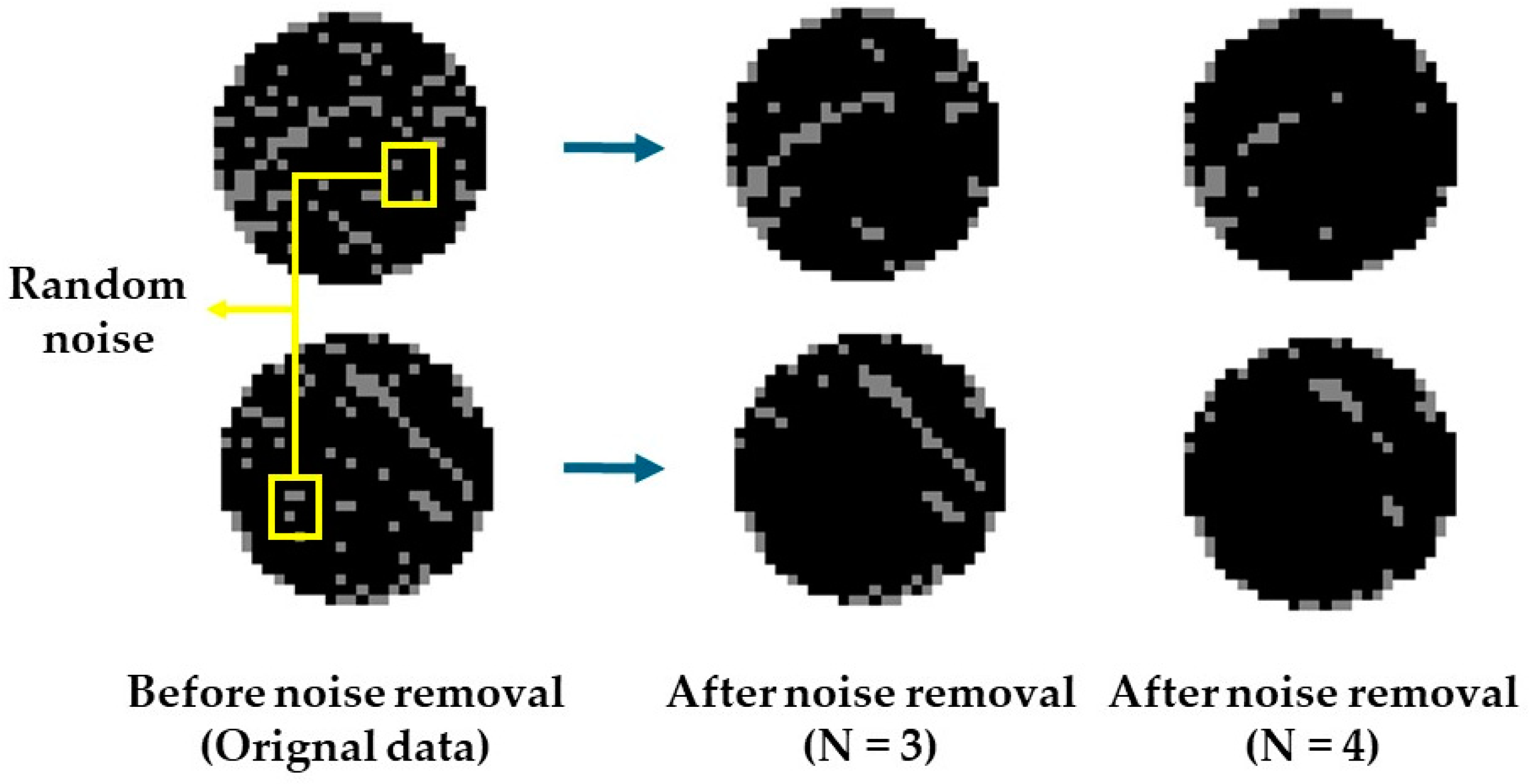
3.2. Random Noise Filtering and Data Augmentation

Figure 1, Figure 2a,b and Figure 4 show that there are randomly located defect dies on the WBM called random noise, in addition to the defect dies that match the typical trend of the defect pattern. In this paper, the term ‘randomly located defect die’ refers to defective dies that are located independently of the characteristics of the typical defect types. These defect dies act as noisy data in the defect pattern classification process. The patterned defect die populations are mainly influenced by controllable factors in the wafer production process, such as process parameters, equipment defects, and improper operation. However, the presence of random noise in wafer production is often due to a lack of process environment management or factors that are difficult to control directly. To reduce random noise, gradual improvement of the process environment or replacement of expensive equipment over a long period of time is necessary [33]. As a result, there are always defect dies corresponding to noise in the WBM. In this case, the number of noise defects degrades the geometric and spatial characteristics of the defect pattern. Therefore, it is necessary to remove random noise before using wafer defect patterns as training data. It is difficult to determine with certainty whether each die is a ‘randomly located defect die’ or not. However, they are typically distributed uniformly across the wafer, similar to salt noise in an image.
In this study, we denoise the center pixel of a 3 × 3 region by converting it to a normal die if there are less than N pixels in the 3 × 3 region that correspond to defective dies. In other words, if the number of defect dies in a 3 × 3 region as shown in Figure 5 is lower than a threshold value, we consider the defect die to be a ‘randomly located defect die’ and define it as ‘random noise’. Figure 5 displays the denoising outcomes based on the threshold N value. In Figure 5, the defect dies in the yellow box are an example of random noise. The image labeled ‘N = 3’ shows an image where noise was removed by setting the N value to 3. Similarly, the image labeled ‘N = 4’ shows an image where noise was removed by setting the N value to 4. The distribution of the ‘Scratch’ defect pattern which has the thinnest defect pattern lost its shape due to excessive denoising when N = 4, as shown in the figure. Therefore, this paper selected N = 3 to eliminate random noise while preserving the defect pattern’s characteristics.
Table 2 shows a significant deviation in the number of data between the ‘none’ type of data and the remaining defect patterns, except for outliers. This data imbalance issue is prevalent in many fields that require training data, not just WBMs. Moreover, it is challenging to rely on the performance of a classification model trained with unbalanced data by class. In this study, we augmented the data using the method of rotating WBM images to balance the number of WBM data by defect type to 250, as shown in Table 3. To achieve this, we sequentially rotated the original data from 15 degrees to 360 degrees, resulting in a total of 24 different angles. The augmented data were then saved separately. If the number of original data presented in Table 2 was insufficient to create 250 datasets, we randomly added augmented data from the separately stored augmented data to create 250 data for each class. Table 3 shows the number of labeled WBMs after outlier removal and augmentation.

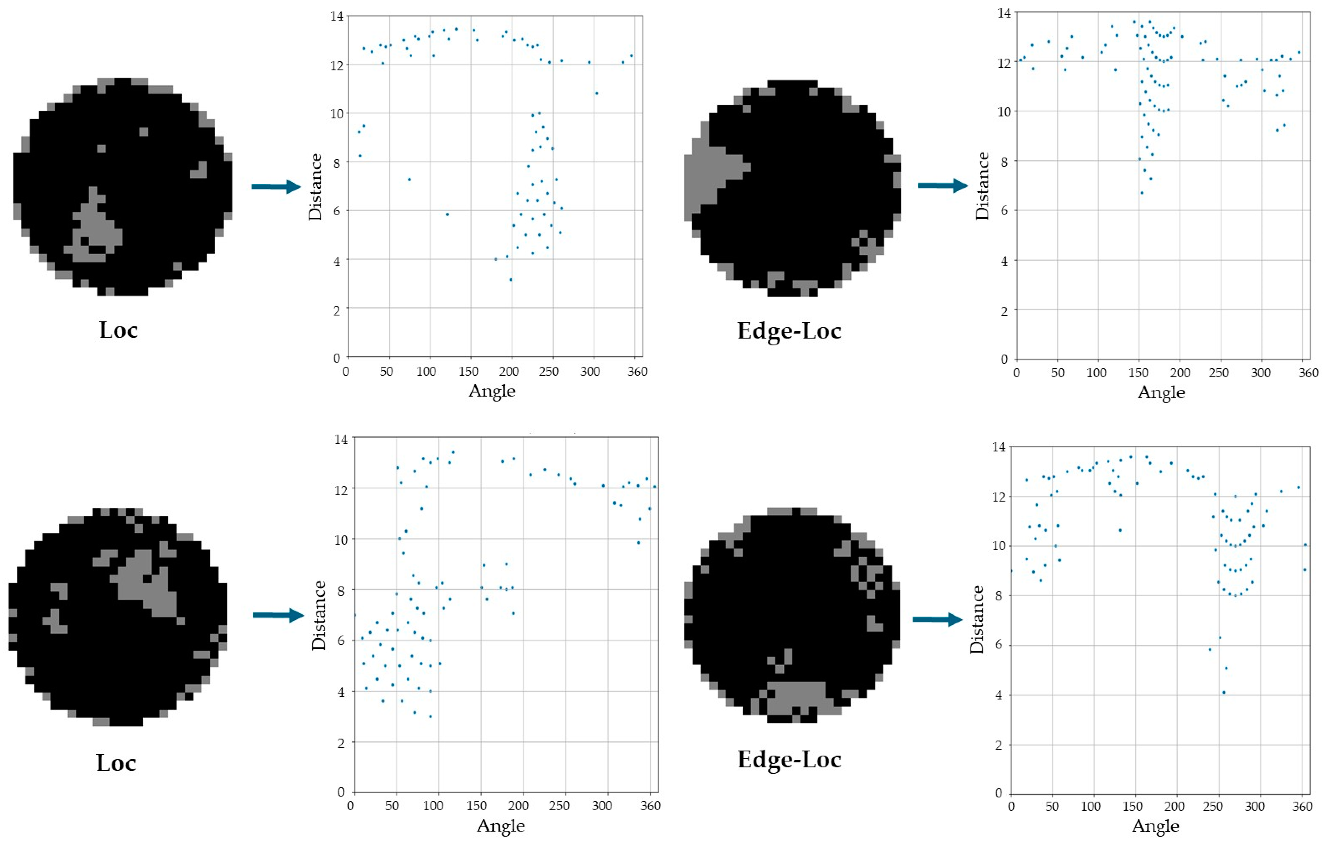
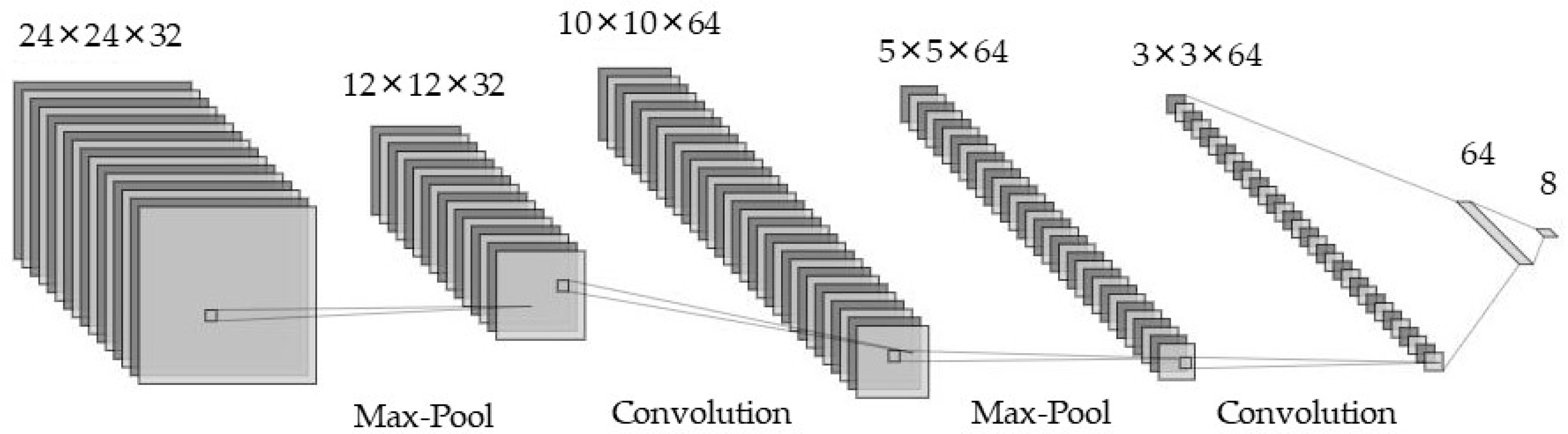
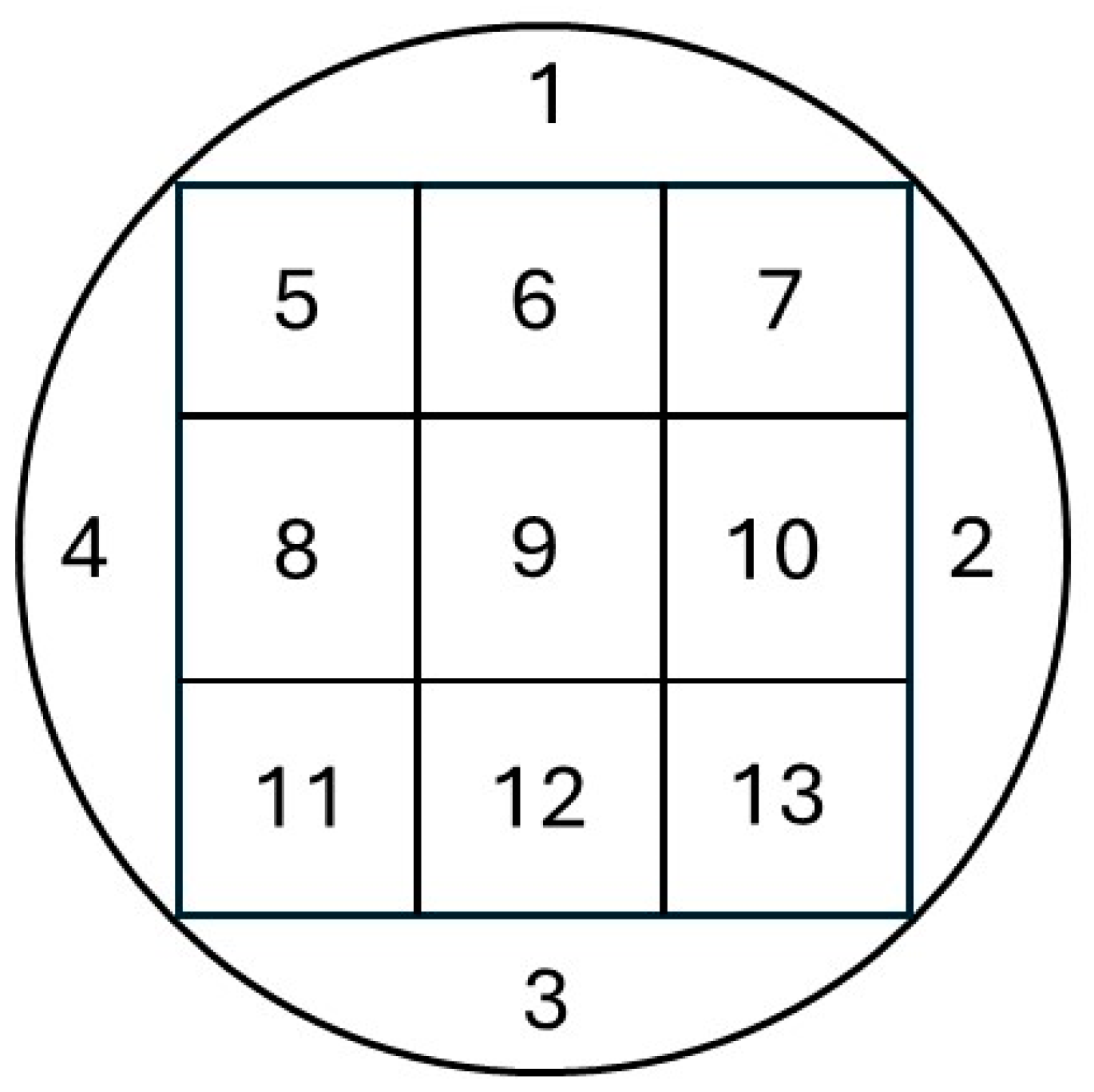
3.3. Defect Pattern Classification Using Polar Coordinate Data

In general, WBM defect pattern classification used two-dimensional image data represented by the Cartesian coordinate system. In this case, the pixel corresponding to the defect die has a spatial coordinate value on the x and y axis as shown in Figure 1. Figure 2a shows that for the ‘Center’ pattern, defects are concentrated in the center of the image. For the ‘Donut’ pattern, defects are distributed in the shape of a donut with a hole in the center, and there are few defects in the positions corresponding to the center and edge. Even when the WBM image itself is used as training data for the classifier, efficient defect pattern classification is possible if the distribution of defect dies in WBM images belonging to a class is independent of the rotation of the pattern in the Cartesian coordinate system, as shown in Figure 2a. However, upon examining the ‘Edge-Loc’, ‘Loc’, and ‘Scratch’ patterns in Figure 2b, it becomes apparent that they belong to the same class but are randomly located in the Cartesian coordinate system representation of (x, y). When the distribution of defect dies is highly randomized for each image, extracting the spatial characteristics of defect dies becomes challenging when training a classifier using WBM images as input.
In this study, we applied the method of converting WBM spatial coordinate information into polar coordinate data to improve defect die distribution characteristics. To achieve this, we obtained the distance from the origin of the WBM by recognizing the defect die as one spatial coordinate value. Then, we calculated the angle of each defect die in the counterclockwise direction with respect to the x axis. The defect die’s distance from the origin is denoted by the variable r, while the angle away from the initial ray is denoted by the variable θ, resulting in a polar coordinate pair of (r, θ).
Figure 6 shows the distribution of the defect dies on the coordinate system after converting the WBM data into a polar coordinate system, where the horizontal axis represents angle and the vertical axis represents distance from the center of wafer. The location information of the defect dies was then used as input to the defect pattern classifier through the following process. The two-dimensional plane data were converted to the polar coordinate system and divided into 49 blocks based on r and θ. Specifically, θ was divided into seven sections from 0 to 360 degrees in increments of 50 degrees, and the distance was divided into seven sections from 0 to 14 in increments of 2. The number of defective dies in each section was measured, and the data were reconstructed into a 7 × 7 matrix-shaped two-dimensional array. The classifier was trained using the polar coordinate system data as input and its performance was compared to the existing classifier trained using WBM images.
This transformation aims to improve the characterization of defect patterns in ‘Edge-Loc’, ‘Loc’, and ‘Scratch’, where the location of defect patterns is inconsistent in the Cartesian coordinate system. Specifically, both ‘Edge-Loc’ and ‘Loc’ patterns, as shown in Figure 6, share the common feature that defect dies are clustered in a certain space, but in both classes, the location of the defect pattern is not consistent, and it is difficult to distinguish them from the image alone. Therefore, to distinguish between these two classes, whether the defect pattern is located at the edge or inside the WBM plays an important role in classification performance. Therefore, it is predicted that the method using polar coordinate system data containing distance information from the origin will be better than the method using WBM images. Furthermore, upon examining the example WBM images in Figure 6, it becomes apparent that the defect patterns’ locations in Cartesian coordinates differ significantly, despite both belonging to the same label as ‘Edge-Loc’ and ‘Loc’, respectively. However, when the location information of defect dies is converted to a polar coordinate system, it becomes apparent that the distribution of defect differences is concentrated on the side farthest from the origin in the case of ‘Edge-Loc’, while in the case of ‘Loc’, the distribution of defect differences is concentrated in the area with a medium distance from the origin.
Figure 7 and Table 4 shows the CNN architecture used in this study. The model comprises three convolutional layers with 32, 64, and 64 channels. The rectified linear unit (ReLU) function was used as the activation function for each layer. After completing all convolutional operations, the layers were reconnected through fully connected layers with 64 and 8 nodes. The output layer consists of neurons that correspond to each failure die pattern, and the softmax function is used as the activation function. The CNN structure was determined by tuning the hyperparameters manually. Adam was used as the optimizer, and the learning rate was set to 0.1, 0.01, and 0.001, which are commonly used values, to compare performance. The batch size was determined by gradually increasing it from a small value to 64, 128, 256, and 512, while the epoch value was sequentially increased from 100 to 300, until the training loss no longer converged. Ultimately, a batch size of 256, a learning rate of 0.01, and 300 epochs were chosen.

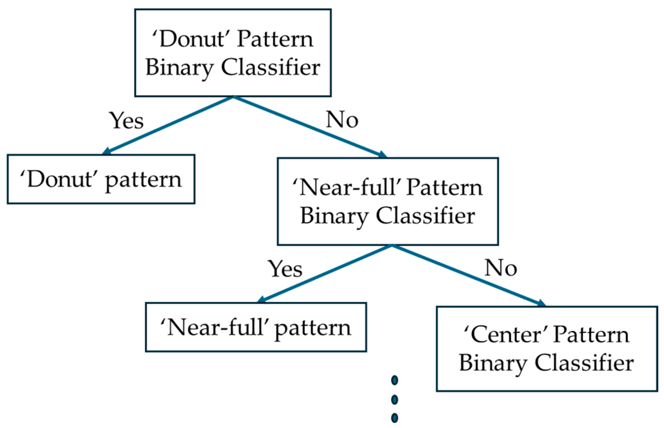
3.4. Defect Pattern Classifier Using Polar Coordinate System Data and Tree Structure

In the previous section, we presented a model for classifying eight defect patterns using WBM information expressed in a polar coordinate system as input to a single CNN. In this section, we present a model that can classify WBM defect patterns through binary pattern classifiers connected in series by applying a tree structure. To classify the eight defect patterns, we created eight binary classifiers that can classify each defect pattern and the remaining patterns. Unlike the conventional decision tree method, which is based on recursive partitioning and pruning and has an indeterminate structure of the whole tree, the proposed model simply connects as many binary classifiers in series as the number of defect patterns to be classified.
The defect patterns in the WBM can be characterized by their location and shape on the plane. Some patterns are distinguishable solely by their location, while others are simply distinguishable by their shape rather than by their location. To simplify these problems, we used a structure with consecutive binary classifiers to classify defect patterns and compared their performance. The most important factors that determine the classification performance for classifiers with this structure are the performance of individual classifiers and the order in which the classifiers are arranged. In this paper, SVM, one of the most popular binary classifiers, and CNN, a representative deep learning method, were used for each node of the tree structure. The order of the classifiers was determined based on their classification accuracy, with the highest accuracy classifiers placed at the top nodes. To reduce errors in classifying other classifiers, we first classify easily distinguishable patterns. To train the binary classifiers for learning individual patterns, we used the 2000 polar coordinate system data presented in Section 3.2 (Table 3). The data were split into a 7:3 ratio for training and test data, respectively. The training data were used with the two outputs relabeled as Applicable/Others for the corresponding patterns.
Figure 8 illustrates the structure of the classifier proposed in this paper. The binary classifier’s classification performance for implementing the model is as follows: ‘Center’: 98.9%, ‘Donut’: 100%, ‘Edge-Loc’: 94.8%, ‘Edge-Ring’: 98.1%, ‘Loc’: 93.5%, ‘Near-Full’: 99.3%, ‘Random’: 98.1%, and ‘Scratch’: 96%. We determined that the characteristics of the defect pattern become more distinct as the binary classifier’s performance improves. Therefore, we placed the patterns with better binary classification performance at the top node. We designed a tree structure for the eight classifiers by first classifying data with a clear defect pattern. Then, we placed the data predicted not to belong to that pattern at the higher classification node back into the lower classification node. The test results and performance comparison of this model are presented in Section 4.

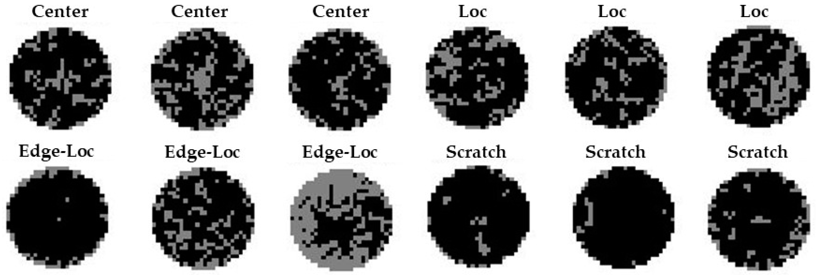
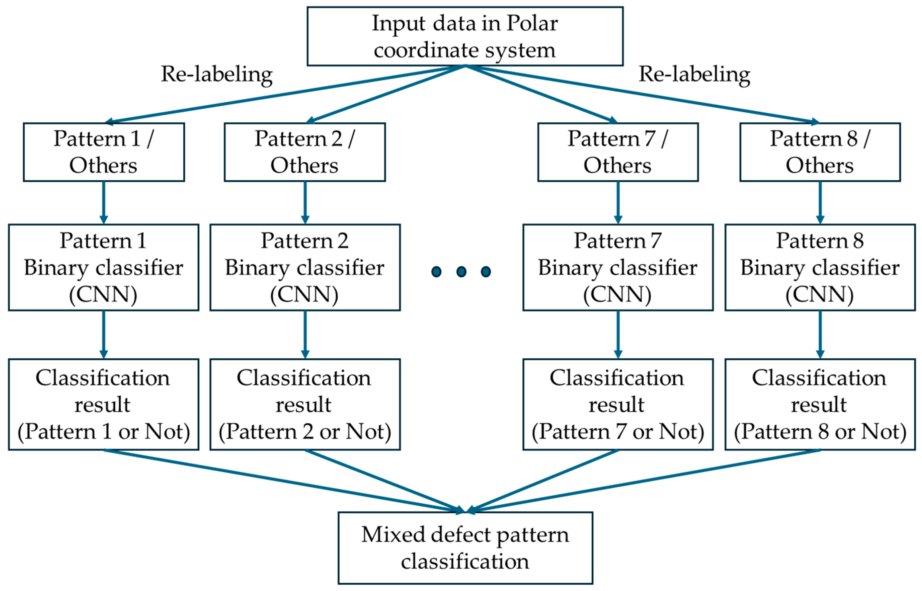
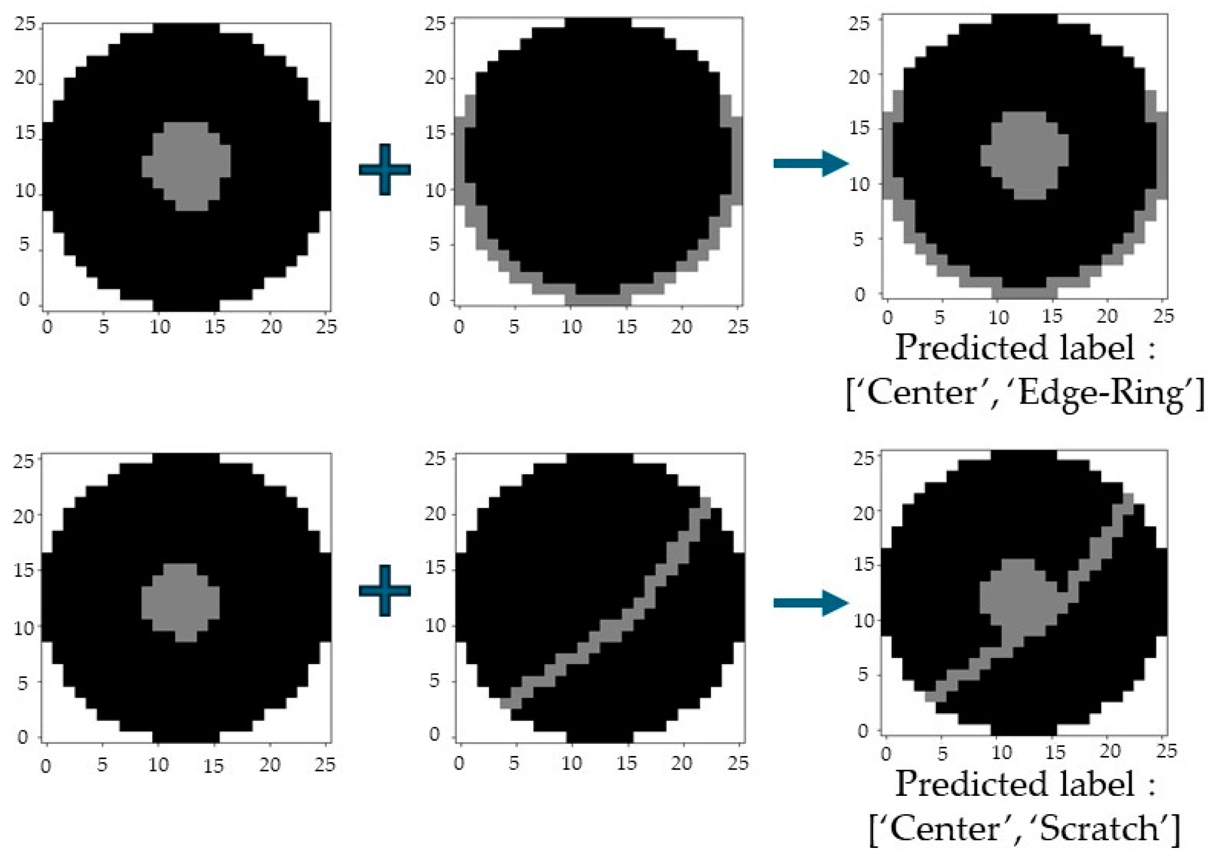
3.5. Ensemble Structure for Classifying Mixed Failure Patterns

In general, the method for separating mixed defect patterns in WBM is to segment multiple defect patterns on a WBM image by applying algorithms such as connectivity filtering or DBSCAN. However, these methods have a drawback in that the number of defect patterns to be segmented varies depending on the size or distribution of defect patterns on the WBM. Additionally, segmentation becomes difficult when other defect patterns are adjacent or overlapped on one defect pattern. In addition, defect dies corresponding to global defects that are not related to the defect pattern have a significant influence on the segmentation process, so it is essential to perform extra data pre-processing before classifying mixed defect patterns.
This paper proposes a method to classify mixed defect patterns by ensembling binary classification models for each class without segmenting the mixed defect patterns to solve these problems. The structure of the proposed classifier is shown in Figure 9. To implement this model, we first relabel the polar coordinate system data presented in Section 3.2 into two categories: the corresponding defect pattern and other patterns, and generate binary classification models for eight defect patterns (Center, Donut, Edge-Loc, Edge-Ring, Loc, Near-Full, Random, and Scratch). Eight classification results are extracted for WBM images from the output layer by ensembling classifiers for each defect pattern. If two or more classifiers indicate that the defect pattern corresponds to the defect pattern, both classes are output to classify it as a mixed defect pattern. By synthesizing these results, we developed a classification model that can determine whether the defect pattern on the WBM is a single defect pattern or a mixed defect pattern and identify which defect patterns are mixed. The ensemble technique used in this paper has a very simple structure, i.e., there are binary CNN classifiers that can distinguish each defect pattern, and their predictions are passed to the mixed defect pattern classification block shown in Figure 9 with same weight for each classifier. In other words, this step acts as a decision network layer in the ensemble network. In this step, the classification result is determined by the soft-voting ensemble method, i.e., the outputs of each binary classifier that exceed a certain threshold are selected to determine that the WBM belongs to the corresponding defect type. For this experiment, we set 0.7 as the threshold value. As a result, each WBM can be classified as either a WBM with only one defect type or a WBM with two or more defect types.
To evaluate this model, we used 877 labeled data points as shown in Table 1. The ‘none’ pattern was not used. The WM-811K dataset’s WBM is labeled as one of the eight bad patterns. If we consider the WBM classification problem using these data as a general pattern recognition problem in machine learning or deep learning, the goal would be to construct a classifier with the highest accuracy based on the labeled values, regardless of the shape of the pattern. Actually, there are many results that approach the research goal to maximize accuracy based on the label of the dataset. However, the labeling of WBMs is subjective and relies on the judgment of semiconductor engineers. In practice, many WBMs are judged as a mixture of two or more defect patterns. Therefore, the original purpose of semiconductor testing is to improve yield by identifying WBM defect patterns. It is necessary to find a more appropriate defect type, even if the accuracy of the original dataset’s labeling cannot be judged by this dataset. In this study, we checked the performance of the ensemble model to classify mixed defect patterns based on the original data, which include all the outlier data shown in Figure 4 and have not been denoised.

4. Experiments and Results

In this study, we conducted experiments and compared the performance of six scenarios, summarized in Table 5, according to the type of input data, the method of pre-processing the input data, and the configuration of the classifier. The scenarios were categorized into single-failure pattern classifiers (Models 1–5) and mixed-defect (failure) patterns classifiers (Model 6), based on the purpose of classifying failure patterns. The single-failure pattern classifiers were further divided into five models according to the type of input data, pre-processing, and classifier type. The performances of Model 1 and Model 2, which used WBM images as training data for the WBM failure pattern classification problem, and Model 3 and Model 4, which used information converted to the polar coordinate system proposed in this paper as training data, were compared at first. To evaluate the performance of the pre-processing method, we have compared the performance of Model 2 and Model 4, which divide the WBM into defined blocks and use the number of defects per block, with that of Model 1 and Model 3, which have no pre-processing. Regarding the classifier, we compared a single CNN trained with the information converted to the polar coordinate system to distinguish between the eight failure patterns (Model 4) and a tree structure based on a binary classifier (Model 5). Finally, we evaluated the performance of the polar coordinate system transformed input-based ensemble of CNN structure (Model 6) for classifying mixed failure patterns.
To compare the classification performance of the model, we used accuracy, precision, recall, and F1-Score as evaluation metrics based on the confusion matrix. In general, the accuracy of a classifier is a representative metric to evaluate the performance of a classifier, but when the data are highly imbalanced, such as the dataset used in this study, the F1-Score is used to evaluate the performance. The calculation method for each metric can be found in Equations (1)–(4) and Table 6.
A c c u r a c y = T P + T N T P + F N + F P + T N
P r e c i s i o n = T P T P + F P
R e c a l l = T P T P + F N
F 1 _ S c o r e = 2     P r e c i s i o n     R e c a l l P r e c i s i o n + R e c a l l
The experiments were performed on an AMD Ryzen 7 3700X 8-core CPU and NVIDIA GeForce RTX 2070 SUPER GPU, using the Keras 2.15.0 open-source library based on TensorFlow 2.15.0. System specifications are summarized in Table 7.

4.1. Comparison of Classifier Performance Using WBM Image Information and Polar Coordinate Information

4.1.1. Comparison of Models Using WBM Image Data as Inputs

For the method that used WBM images as training data, we checked the classification performance of the model that trained the image of WBMs (Model 1) and the model that used the number of defect dies in the specified area as training data (Model 2). To evaluate the performance of the classifier constructed using the WBM image itself as training data, the 2000 pre-processed data shown in Table 3 were divided into 7:3 for training and testing and a 3-fold cross-validation method was implemented. Figure 10 shows a visualization of the classification results in the form of a confusion matrix of Model 1. The model shows a large number of misclassifications between the ‘Edge-Loc’ and ‘Loc’ patterns among the eight defect patterns. The reason for the large misclassification is that the labeling decision may vary depending on subjective judgment compared to other defect patterns. However, the model classified ‘Scratch’ as ‘Loc’ for 19 WBMs. This is likely due to the model’s inability to learn the defect pattern features of the Scratch pattern. The CNN model using the WBM image of WBMsshowed a classification accuracy of 86.5%, precision of 0.86, recall of 0.85, and F1-Score of 0.85.
Model 2 is a model that adds a pre-processing method to Model 1. That is, the WBM data was divided into 13 zones on the wafer plane as shown in Figure 11, and the number of defective dies corresponding to each zone was counted. This pre-processing method reflects the spatial characteristics of the defect variation in the Cartesian coordinate system, which is helpful when comparing performance with classifiers that use the input transformed to polar coordinate space. The data used in Model 2 are the same as in Model 1, consisting of 2000 pre-processed data points summarized in Table 3. The data were divided into 70% training and 30% test data, and the 3-fold cross-validation was used to implement the CNN model. The confusion matrix of the model is shown in Figure 12. Similar to Model 1, there were many cases where ‘Edge-Loc’ and ‘Loc’ were not properly identified. However, while Model 1 often misclassified ‘Scratch’ as ‘Loc’, Model 2 also misclassified ‘Loc’ as ‘Scratch’. Model 2 achieved a classification accuracy of 82%, precision of 0.86, recall of 0.85, and F1-Score of 0.85, which is similar to Model 1. However, its accuracy was 4.5% lower, indicating that the pre-processing may not be suitable for modeling methods that utilize WBMs as input.

4.1.2. Comparison of Models Using Polar Coordinate System Data as Inputs

In the case of using polar coordinate system data as training data, we evaluated the performance of each classifier by implementing a model trained on the image data themselves and a model trained on the number of defect dies in a given region. To represent the defect dies on the WBM in the polar coordinate system space, we obtained the distance from the center point of the WBM and calculated the angle of each defect die in the counterclockwise direction. The first variable, r, specifies the distance between the defect die and the center point. The second variable, θ, specifies the angle value away from the initial ray, generating polar coordinate system data in the form of (r, θ) polar coordinate pairs, and the data were used to train the model. The 2000 pre-processed data shown in Table 3 were divided 7:3 to be used as training and test data, and a 3-fold cross-validation method was applied. Model 3 exhibited a classification accuracy of 79.5%, with a precision of 0.79, recall of 0.78, and F1-Score of 0.78. These results are slightly lower than the previous model that used WBM images as input.
Figure 13 shows the confusion matrix for the classification performance of Model 3. Overall, the failure to distinguish between the ‘Edge-Loc’ and ‘Loc’ patterns is similar to Models 1 and 2. Although the advantages of using polar coordinate transformations to represent spatial information in defect images were demonstrated in Section 3, the representation of coordinates corresponding to the defect die as points in polar coordinate space may be limited. In other words, the defective die, previously represented with a resolution of 26 × 26 in the WBM, is now represented as a single point in the polar coordinate system, as shown in Figure 6. At this time, the polar coordinate system information (r, θ) is converted so that the r value in the range of 0–14 and the θ value in the range of 0–360 degrees are expressed to the second decimal place. In other words, the position of the defective die that was expressed with a resolution of 26 × 26 is expressed as a point on a plane with a resolution of 1400 × 36,000. Consequently, the proportion of the total area occupied by the defect dies in the WBM represented in the polarized plane is much smaller than the area of defect dies in the WBM before conversion, even when the same number of defective dies are represented on the plane. In other words, the amount of information on defect dies is relatively small compared to the total area of the WBM used as input.
Therefore, the current representation provides only a limited amount of information for learning compared to the amount required to learn the entire space of the polar coordinate system. As a result, proper learning cannot be achieved. Therefore, it is estimated that the classification performance of Model 3 was inferior, and to improve it, a pre-processing method is required.
Model 4 includes a pre-processing step to solve the problem of Model 3. As described in Section 3.2, the angle θ is divided into seven levels of 50 degrees from 0 to 360 degrees and the distance is divided into seven levels of 2 from 0 to 14, a total of 49 sections, and then the number of defective dies belonging to each section is measured and reorganized into two-dimensional array data with a 7 × 7 matrix shape. This method reduces the resolution of the location of the defective die in polar coordinate space. However, it enables expression of the degree of existence of the defective die by the weight.
As with other models, Model 4 was implemented using a 7:3 ratio of pre-processed data summarized in Table 3 for training and testing and a 3-fold cross-validation procedure for implementing the CNN model. Model 4 achieved a classification accuracy of 91.3%, precision of 0.91, recall of 0.91, and F1-Score of 0.91, which are significantly higher than those of Model 3 and superior to models that use existing WBM images as input in all evaluation metrics. The confusion matrix of the model is shown in Figure 14. Although there is a slightly higher error rate in distinguishing between the ‘Edge-Loc’ and ‘Loc’ patterns compared to other defect patterns, the overall error rate is still very low when compared to other classifiers. Additionally, there is no bias towards any particular failure pattern.
Table 8 summarizes the classification performance of the four models. Model 4, which uses polar coordinate system information as input for region segmentation pre-processing, shows the best performance in almost all evaluation metrics, as shown in the table. Especially for ‘Edge-Loc’, ‘Loc’, and ‘Scratch’ patterns, which are considered to have high defect pattern randomness, the scores of all evaluation metrics are significantly increased. For ‘Edge-Loc’ and ‘Loc’ patterns, the defect pattern can either exist at the edge or inside the WBM. However, there is a commonality that the defect dies are clustered in a certain space. It is believed that classification results using polar coordinate system data containing distance information from the origin are superior to image data. It was found that pre-processing with the number of defective dies using region segmentation was very useful for the classification when using polar coordinate system data as input. However, this pre-processing method did not improve performance when using Cartesian coordinate system data. This is attributed to the difficulty of clustering ‘Loc’ and ‘Edge-Loc’, which are represented by various (x, y) values in the Cartesian coordinate system, as described in Section 3.2, and the pre-processing would not be helpful in this case.

4.1.3. Comparison of Classification Performance of WBM with Different Die Size from Training Data (Model 1 and Model 4)

In this paper, we have confirmed that the method based on the number of defect dies per specified region in polar coordinate space as training data can improve the defect pattern classification performance compared to the method based on conventional WBM image data. However, the test results are limited to WBMs of 26 × 26 in ssize, so the performance cannot be confirmed when the die size or number of dies per wafer is different. To test the scalability of the proposed method, we conducted defect pattern classification on all labeled WM-811K WBMs, regardless of wafer dimension and die size.
Table 9 summarizes the number of labeled WBMs in WM-811K by defect pattern type. All 25,519 of the 172,950 labeled data, except for the ‘none’ pattern, were resized to 26 × 26. This means that the pixel corresponding to each die in the WBM image was resized to reduce or increase the number of dies. The next step is identical to the process described in Section 3.2: denoise the data, convert them to polar coordinates, and create a classifier that measures the number of defective dies per specified region in polar coordinate space. Additionally, as a comparison group, a classification model was created using the original WBM image without the polar coordinate system conversion. For both models, data were divided by 7:3 for training and testing and then 3-fold cross-validation was performed for modeling.
Table 10 shows the classification results for 25,519 WBMs with different sizes than the WBMs used for training. The classifier that used WBM image data as input has an accuracy of 85.58%, while the classifier that used polar spatial information as input has an accuracy of 89.89%. Moreover, the model that used polar spatial information as input outperforms the model that used WBM image data in most other metrics. Both models performed about 2% less accurately than when tested on 26 × 26 WBMs alone. This is due to the fact that cases with incorrect or ambiguous labels are removed when training and testing on 26 × 26 WBMs only. For this test, we used all 25,519 WBMs for testing without removing outlier data, as it would have been inefficient from a time and labor perspective to manually check all 25,519 WBMs. The experiment confirmed that classifying defect patterns by converting WBM image data to polar coordinate data performs better than using WBM image data alone, even when using all labeled data in WM-811K without removing outliers. Therefore, we expect that the proposed classifier can be used without additional training by resizing WBMs that are not the same size as the WBMs used for training.

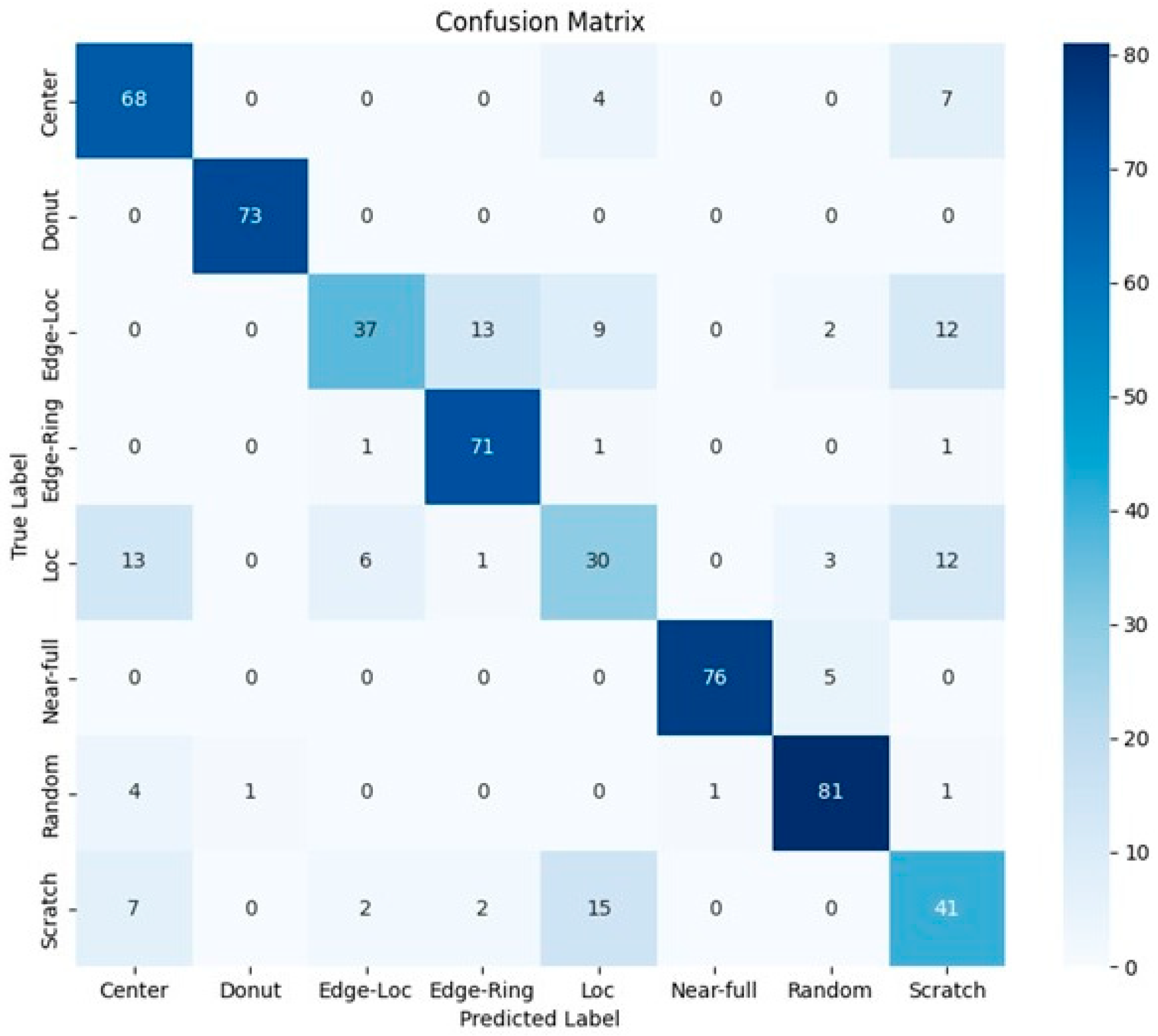
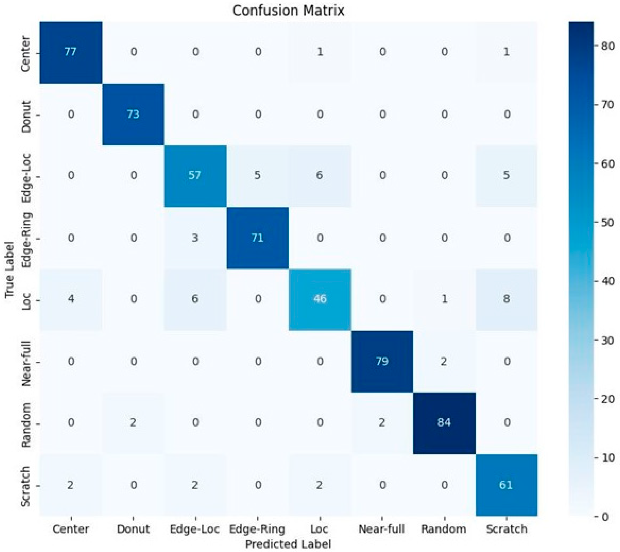
4.2. Defect Pattern Classifier Based on Polar Coordinate System Input Data and Tree Structure

To implement the defect pattern classifier based on the polar coordinate system data and tree structure described in Section 3.3, we first created a binary classifier for each defect pattern. The training data were selected based on the experimental results presented in Section 4.1, using Model 4, which showed the best classification performance. In Section 4.2, we did not classify the defect patterns into eight classes. Instead, we created eight binary classifiers, each for a specific pattern. To achieve this, we implemented a model using support vector machine (SVM), which is a representative machine learning algorithm for binary classification. We then compared its performance with the binary classification model based on the CNN. The training data to test data ratio was set to 7:3 for both SVM and CNN models. The structure of the CNN model is shown in Figure 7 with two output layers. A batch size of 256, a learning rate of 0.01, and 300 epochs were used and three-fold cross-validations were performed.
Table 11 shows a comparison of the binary classification performance of the two models. As indicated in Table 11, the CNN model outperforms the SVM model on most performance metrics. Regarding the SVM model, similar to the classification results in Section 4.2, the performance is poor for ‘Edge-Loc’, ‘Loc’, ‘Random’, and ‘Scratch’ patterns, which are considered highly randomized defect patterns. This is due to SVM’s binary linear classification model, resulting in low performance for classes with high randomness between patterns. Therefore, we used CNN-based binary classifiers for each node of the tree-structured classifier.
To implement a tree structure classifier, we first divided the 250 data for each class shown in Table 3 into a 7:3 ratio and stored them separately as training and test data. Then, we created binary classifiers for each of the eight classes by re-labeling the training data as Pattern/Others and training the CNN model. The binary classifiers in the tree structure are ordered sequentially, starting from the pattern with the best binary classification performance in the above experiment, i.e., Donut, Near-Full, Center, Random, Edge-Ring, Scratch, Edge-Loc, and Loc, according to the experimental results. Figure 15 displays the confusion matrix of the binary classification results for each level of the tree structure. The model’s overall classification accuracy was 94%, with successful class predictions for Donut (75), Near-Full (75), Center (72), Random (73), Edge-Ring (72), Scratch (71), Edge-Loc (69), and Loc (57), totaling 564. In total, 36 data points out of 600 WBMs failed to predict.
Table 12 compares the classification results of Model 4 in Section 4.1 with those of Model 5 which used a tree structure. Both models use the number of defect dies per specified region in polar coordinate space as training data, so there is no difference in the type of data trained, only the structure of the classifier. Table 12 shows that Model 5 outperforms Model 4 on most metrics. The table displays the classification results for each defect type in Model 5. These results are based on the binary classification results of each node in the tree structure. The average value is the arithmetic mean of the results for each defect type. The overall classification accuracy is 94%, while the arithmetic mean of the accuracy is 97%, which is expressed differently. Despite this, Model 5 still exhibits higher classification performance than Model 4. It has been confirmed that using a tree-structured method to classify defect patterns sequentially, based on classifiers with high binary classification performance, can improve the accuracy of defect pattern classification.
However, this model has a limitation in that it cannot be used to classify mixed defect patterns with more than two defects. Additionally, the classification result of the entire sample is obtained by sequentially connecting classifiers, resulting in varying amounts of data to be classified depending on the position of each binary classifier. For instance, in this experiment, the number of data inputs to the classifier at the first node was 600, while the number of data inputs to the classifier at the last node was only 72, which accounts for approximately 12% of the initial input data. Therefore, it is not reasonable to accept the evaluation metrics presented in Table 12 as a one-to-one comparison in such a situation with a significant variation in the amount of input data. Further analysis is necessary to address this issue after securing more comprehensive data.
Similar to the extensibility experiment of Model 4, we used Model 5 to classify 25,519 data labeled with defect pattern type among WBMs other than 26 × 26 in size. The denoising and pre-processing process, including how to convert the original data to 26 × 26, and the ratio of training and testing subjects were the same as in Model 4. In this experiment, the order of the binary classifiers in the tree structure was determined by placing the classifiers with the best binary classification performance at the top nodes sequentially. However, the order of the classifiers differed from that obtained using only the 26 × 26 WBM. For this experiment, each binary classifier was placed in the following order: Near-Full, Donut, Random, Center, Scratch, Edge-Ring, Loc, and Edge-Loc.
The confusion matrix of the binary classification results for each level of the tree structure is presented in Figure 16. Out of 7658 test data, 6225 were successfully predicted, while 1433 data failed to be predicted, resulting in an overall classification accuracy of 81.2%. The predicted data are shown as Near-Full: 35, Donut: 129, Random: 181, Center: 1194, Scratch: 135, Edge-Ring: 2762, Loc: 671, Edge-Loc: 1118. The binary classifier exhibited the lowest performance, with the most misclassifications occurring in the ‘Edge-Loc’ pattern classification. There was also a noticeable error in classifying ‘Edge-Loc’ patterns as ‘Other’, but especially in misclassifying WBMs that were not labeled as ‘Edge-Loc’ as ‘Edge-Loc’.
Table 13 summarizes the evaluation metric values of the classifier for each type of defect. As mentioned in the previous experiment, the classification results for each defect type shown in this table are based on the binary classification results of each node in the tree structure. The average value is the arithmetic mean of the results for each defect type. The table displays an arithmetic mean accuracy of 93%, while the overall classification accuracy is 81.2%. The binary classifiers have an accuracy rate of at least 93% to 99%, with the exception of the ‘Edge-Loc’ and ‘Loc’ pattern classifiers. However, the ‘Edge-Loc’ pattern classifier has an accuracy rate of only 77%.
It is expected that there is a trade-off between the precision and recall values among the evaluation metrics, but the binary classifiers in Model 5 showed too much difference in these values for each classifier. For example, the classifier for the ‘Scratch’ pattern had a precision value of 0.92 and a recall value of 0.40, resulting in a large difference. In other words, the classifier’s performance was poor as it failed to classify more patterns as ‘Scratch’ than those that were not. The F1-Score value was only 0.56.
The tree-based Model 5 showed higher classification performance than Model 4 in the defect pattern classification problem of 26 × 26 WBMs, but in the classification problem of WBMs of different sizes, the accuracy was 8.69% lower than that of Model 4. The classifiers exhibited a significant difference in recall values for each defect type, resulting in a lower overall F1-Score.
Table 13 shows the variation in data quantity among each class in the training process of the binary classifier used in the corresponding tree structure and it is estimated to be a factor affecting the performance of the classifier. In summary, if the process of learning the features of the defect pattern class with a small amount of data is heavily influenced by the data trained as ‘Others’ with a relatively large amount of data, it is expected to be affected by the data imbalance problem. This can cause a stronger tendency to classify as ‘Others’ in the binary classification process. In general, if there is a data imbalance problem in the original data, it can be solved by using the data augmentation method. However, in Model 5, the degree of data imbalance varies depending on the location of the binary classifier. As a result, it is considered that Model 4 is more appropriate than Model 5 in terms of the scalability of the classification task.

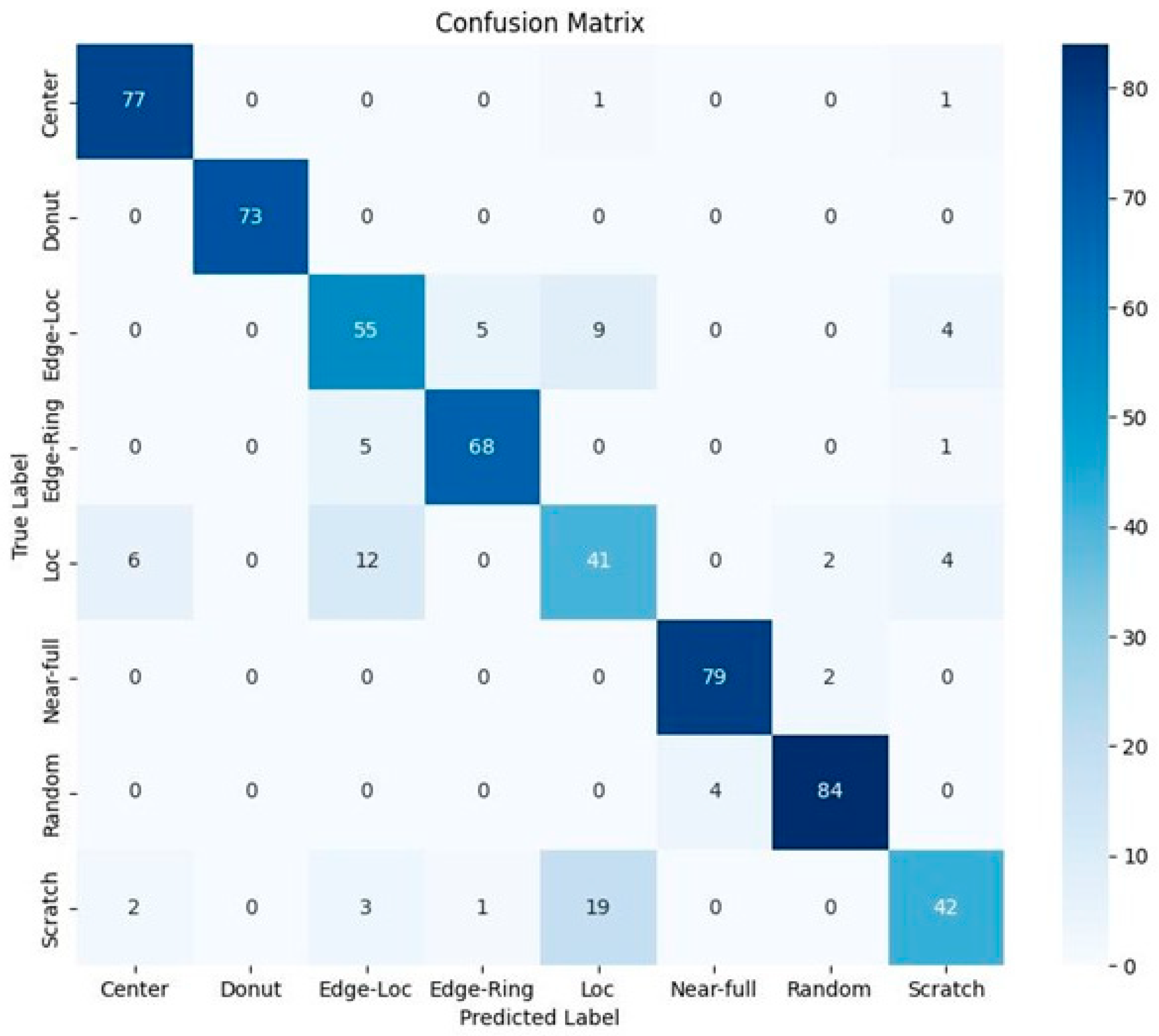
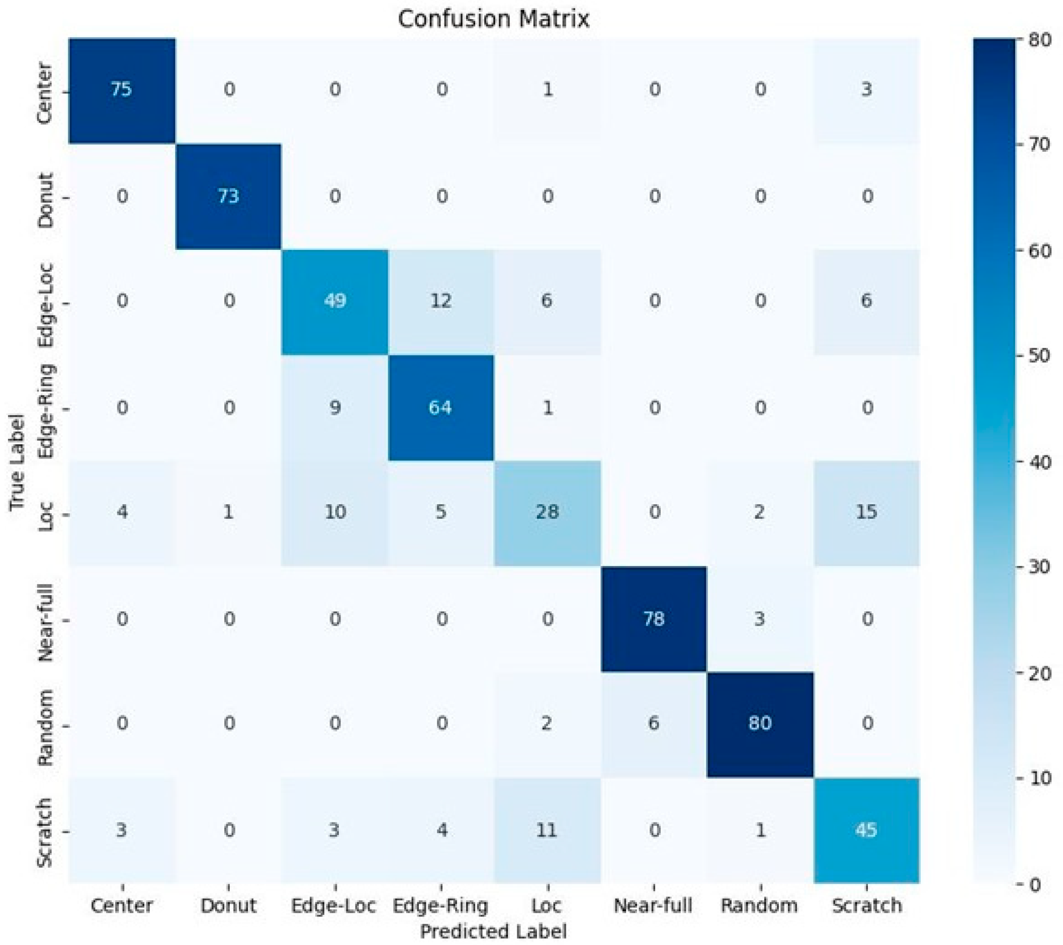
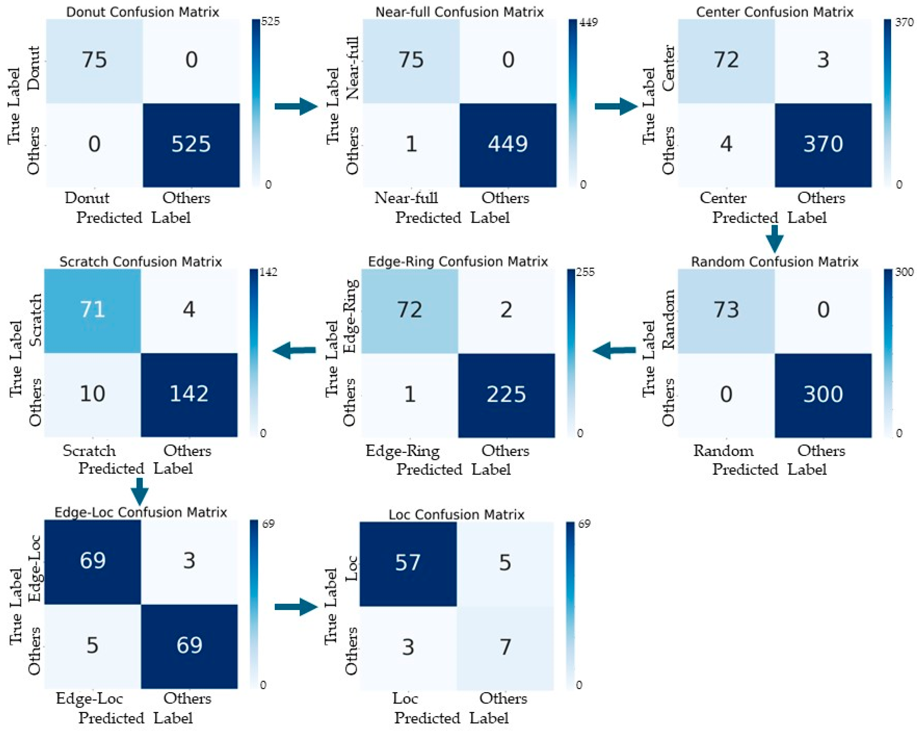
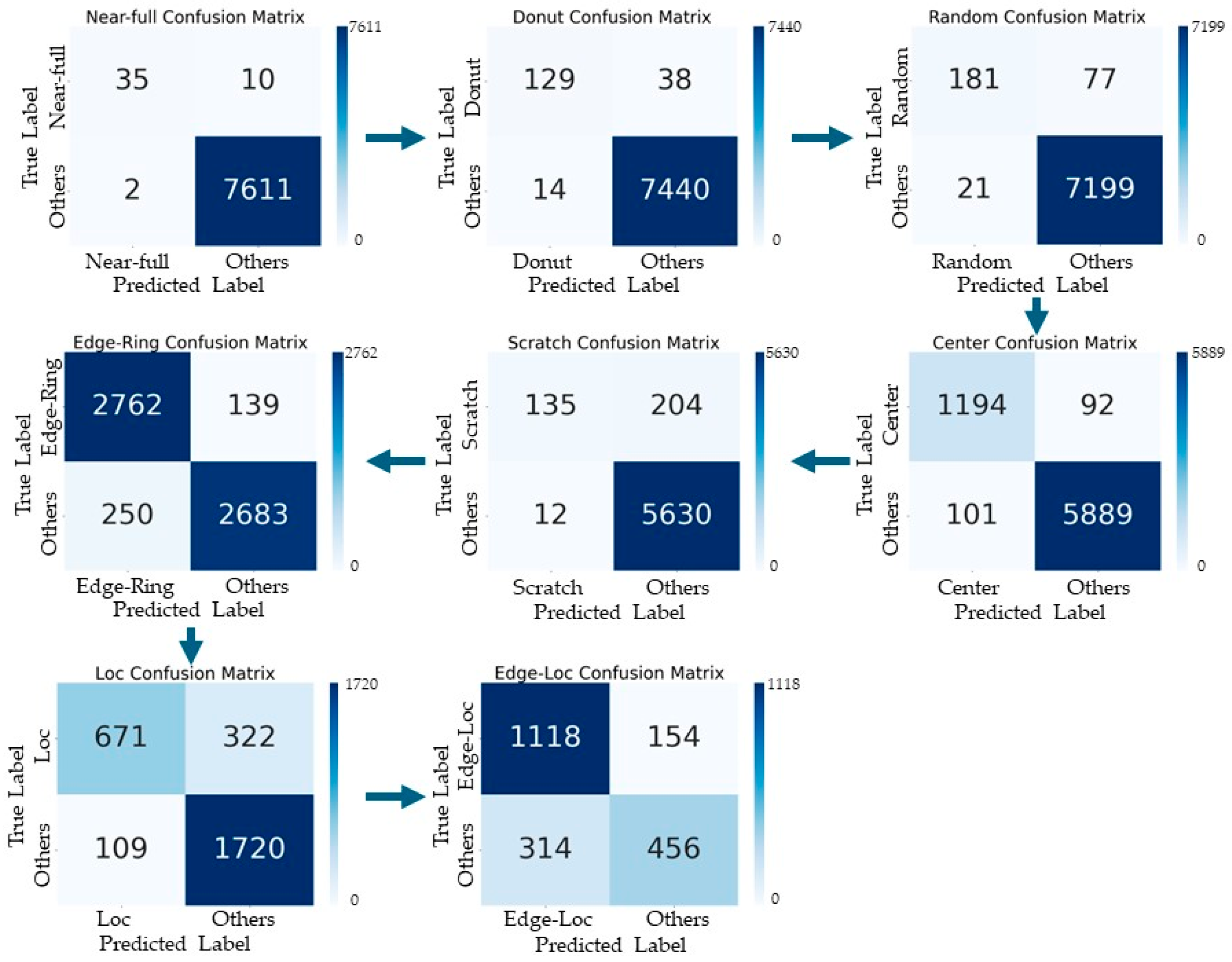
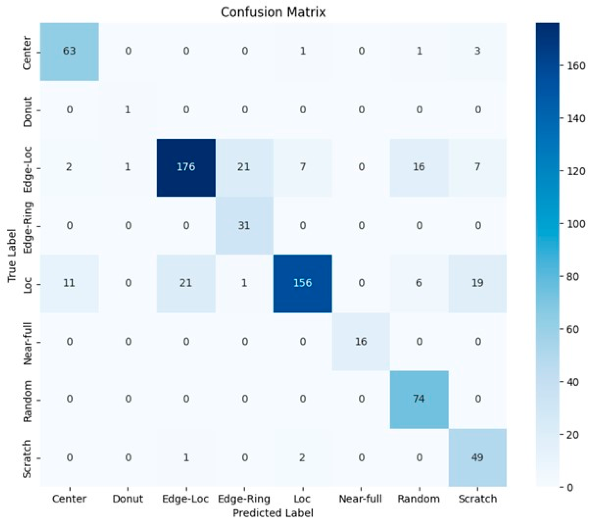
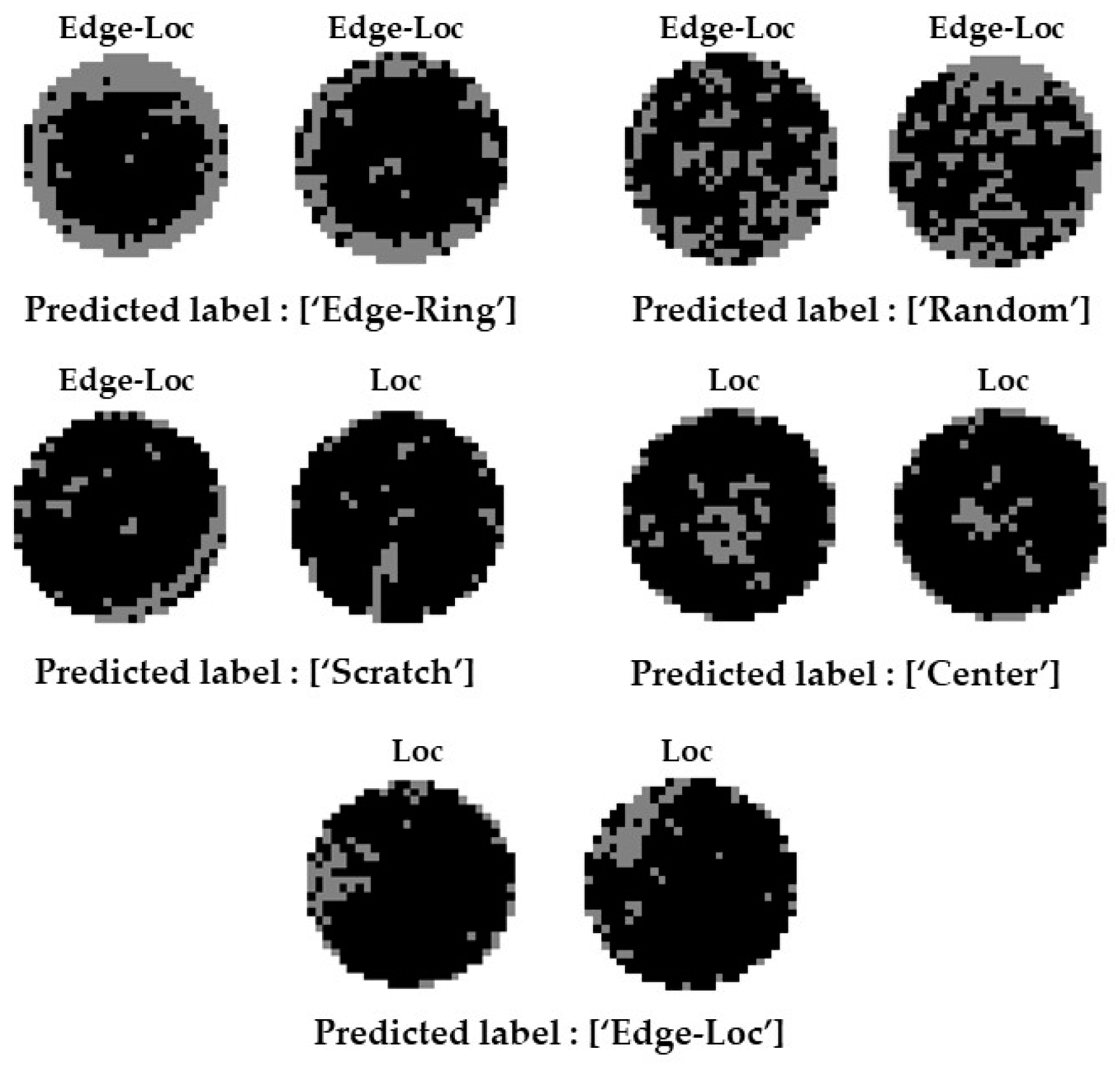
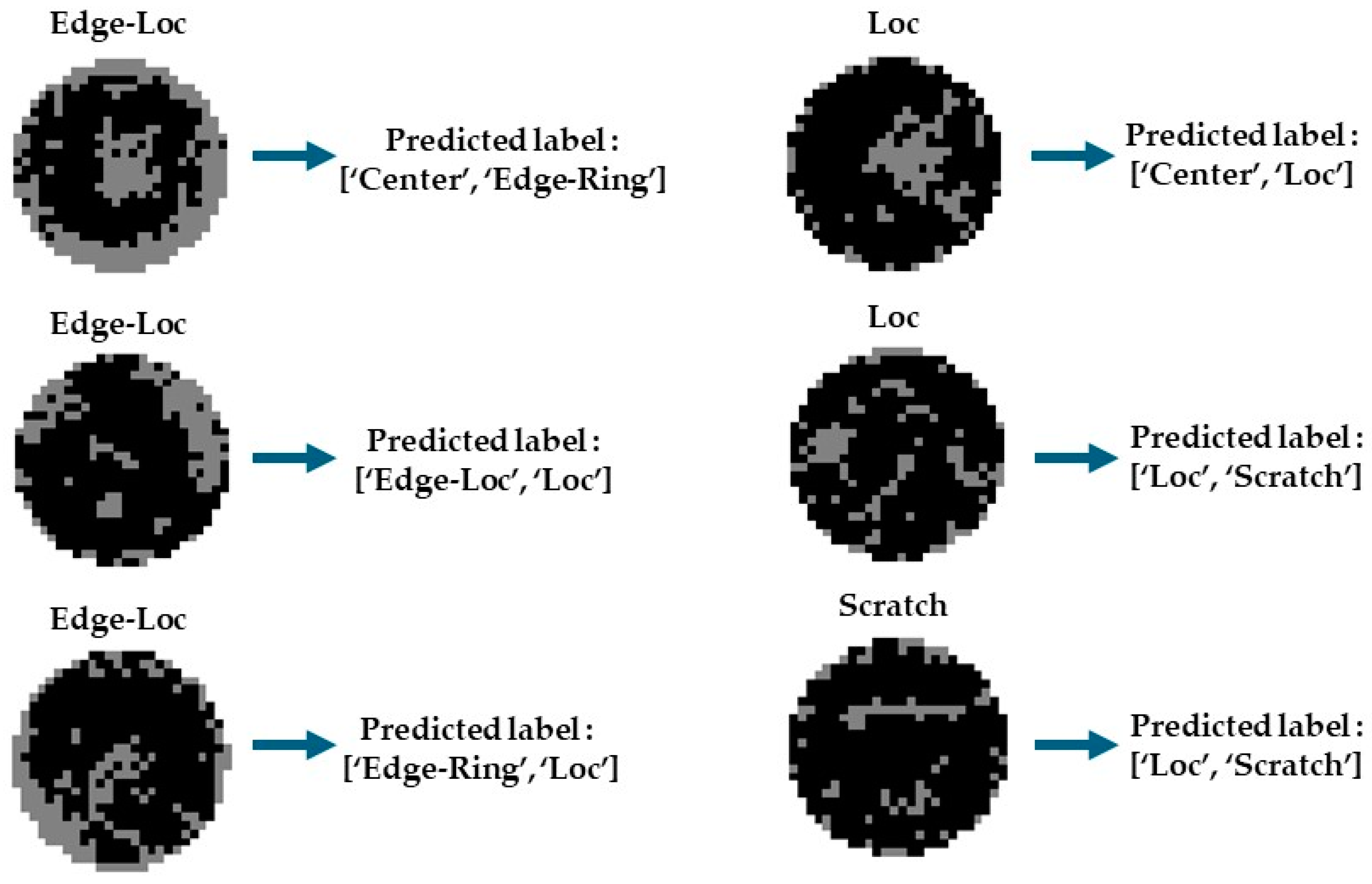
4.3. Ensemble Models for Mixed-Fault Pattern Classification

To implement the mixed defect pattern classifier using polar coordinate system data and the ensemble structure presented in Section 3.4, we selected the training data of Model 4 since it demonstrated the best classification performance in the experimental results shown in Section 4.1. Then, for each class, we relabeled them into two classes: corresponding pattern and other patterns, and generated binary classification models for each of the eight defect patterns (Center, Donut, Edge-Loc, Edge-Ring, Loc, Near-Full, Random, and Scratch). The CNN-model-based binary classifiers have the CNN structure depicted in Figure 7 with two output layers. The training data to test data ratio was set to 7:3, with a batch size of 256, a learning rate of 0.01, and 300 epochs. And three-fold cross-validation was conducted. The binary classification models were connected in parallel, and the output from each model for each test WBM was aggregated for a total of eight outputs. In this step, the classification result is determined by the soft-voting ensemble method and we set 0.7 as the threshold value.
From the original data of 26 × 26 in size shown in Table 1, we excluded the ‘none’ pattern and used the remaining 877 WBMs as test data. Since these data are the original data before removing the outlier data, it is appropriate to use them as test data for the model because they contain images that are difficult to judge with a specific label or contain mixed defect patterns, as shown in Figure 4.
As stated before, the dataset considered in this paper is labeled with only one defect pattern per WBM, so the classification accuracy of mixed defects cannot be evaluated using this dataset. To evaluate the model, we temporarily generated WBMs with typical defect types, as shown in Figure 17, to test the classification of the mixed-pattern WBMs. As shown in the figure, the mixed patterns were output as [‘Center’, ‘Edge-Ring’], [‘Center’, ‘Scratch’], respectively, to confirm that the model classified the mixed-defect patterns correctly.
Table 14 shows the mixed-type pattern classification results of the 877 WBMs. The ‘Labeled Defect Type’ column indicates the type of defect pattern labeled in the dataset. The table presents the pattern classification results for the 877 test data points and the corresponding defect types. In this model, 161 data points labeled as ‘Center’, ‘Edge-Loc’, ‘Loc’, and ‘Scratch’ out of the total 877 WBMs were classified as ‘none’, which means that there is no defect. The data classified as having no defect pattern mostly consisted of images like those shown in Figure 4, which are difficult to identify as having any defect pattern. Therefore, it is assumed that all eight binary classifiers classified them as not belonging to any class.
Figure 18 shows the confusion matrix for 686 patterns that were classified as a single-defect pattern. The most frequent patterns were ‘Edge-Loc’ and ‘Loc’ patterns, which the classifier predicted as other patterns. The reason for this can be confirmed by checking the WBMs that were classified differently from the labeling values. Figure 19 presents some of the WBMs that the classifier classified differently from the label. This figure illustrates that there are instances where the label and pattern shape are inappropriate or uncertain. In other words, it seems that the error is caused by the error in labeling rather than the error in the classifier.
The classifier predicted 30 WBMs out of a total of 877 WBMs as mixed-defect patterns. These patterns were originally labeled as ‘Edge-Loc’, ‘Loc’, and ‘Scratch’. Figure 20 shows an example of a WBM image that was predicted to be a mixed-defect pattern. As shown in the figure, the proposed classifier correctly classified the mixed-defect patterns in the WBM image without any additional clustering process. This demonstrates the feasibility of categorizing mixed-defect patterns using a model that combines binary classifiers built for each of the eight classes in a parallel structure. Figure 21 shows an example of a mixed-defect pattern that the proposed model judges as a mixed-defect pattern, but the result is ambiguous depending on the engineer’s judgment.
Both ‘Edge-Loc’ and ‘Loc’ patterns have the common feature that the defects are clustered in a specific area, but the defect pattern is located at the edge of the wafer in the case of ‘Edge-Loc’ and inside the wafer in the case of ‘Loc’, so the patterns can be classified based on these features. However, if a defect pattern is located on the WBM at the boundary between the edge and the inside of the wafer, even if there is only one characteristic defect pattern, the mixed-defect pattern classifier connected in parallel will determine that both the ‘Edge-Loc’ pattern classifier and the ‘Loc’ pattern classifier are defect patterns of the same class. In this scenario, the classifier’s output layer extracts two classes, and a WBM with a single characteristic defect pattern can be classified as a mixed-defect pattern. When dealing with a combination of ‘Center’ and ‘Loc’, a single-defect pattern’s classification as a mixed-defect pattern depends on its spatial location. This issue requires further verification and research based on securing data accumulated through the process of labeling mixed-type defect patterns according to the engineer’s judgment.

5. Discussion

The experimental results of six models confirm that the proposed polar coordinate system conversion method and pre-processing method can improve the WBM defect pattern classification performance. In examining the confusion matrix of Model 1, which was trained on the WBM image itself, it becomes apparent that the majority of misclassifications were found in the classes associated with ‘Edge-Loc’, ‘Loc’, and ‘Scratch’. These classes present limitations in terms of specifying the location where the defect patterns are distributed. The defect die clusters’ spatial randomness during the WBM image learning process, as described in Section 3.3, led to lower classification accuracy in these classes. Model 3 aimed to solve the problem by using polar coordinate transformed inputs but this approach actually resulted in a decrease in the classification accuracy. The reason for this is that the number of points corresponding to a single defective die is relatively small compared to the polar coordinate space. When the resolution of the location information expressed in 26 × 26 is converted to polar coordinate space, the features of the defective die are not properly learned. To address this limitation, Model 4 applies a pre-processing process that divides the polar coordinate space into regions of a certain size and measures the number of defective dies included per specified region. This model has the highest classification accuracy among the models compared in this paper. We confirmed that the model is applicable to the defect pattern classification test of WBMs with different die sizes than the WBM used for training. For the tree-structured model (Model 5), which connects binary classifiers sequentially instead of using a single CNN, the classification accuracy is 94%. This is an improvement over Model 4, which classifies eight defect patterns at once. However, in the defect pattern classification test of 25,519 WBMs with different die sizes than the ones used for training, the accuracy is lower than that of Model 4. This is likely due to the model structure’s inability to overcome the data imbalance problem of the binary classifier itself and the variation in the amount and characteristics of the test data depending on the node where the binary classifier is located. Therefore, for the single defect pattern classification problem of WBM, Model 4 is considered to be the most appropriate among the models tested in this paper.
Table 15 shows the performance comparison of the model proposed in this paper with the results of several studies that classify WBM defect patterns using the WM-811K dataset. C.-Y. Wang et al. [13] classified defect patterns by implementing a general model using the MobileNet V2 algorithm and a lightweight model with 24.77% fewer parameters. T. Tziolas et al. [18] proposed a methodology for classifying WM-811K by using different data processing techniques for each class to address the issue of data imbalance. Ebayyeh et al. [19] proposed a data augmentation method for classifying WM-811K by using different data processing techniques for each class to address the issue of data imbalance. Q. Xu et al. [22] utilized a model based on ResNet18 with the CBAM algorithm and classified the defect patterns using the cosine normalization method to overcome the data imbalance problem. Although these studies used the same dataset, each model was trained and tested on different data. In some cases, all labeled data in the dataset were used for testing. However, if the number of test data is increased through data augmentation, it becomes difficult to verify the objectivity of the labels of the augmented data. However, if we disregard this point and compare the models’ classification accuracy, the model proposed in this paper has an accuracy 2.56% lower than that of the best model in the existing results. Nevertheless, the F1-Score of the proposed model is higher than that of the comparison models, indicating that the polar coordinate system transformation and the data pre-processing method presented in this paper have achieved significant results in defect pattern classification.
If the goal of this paper is simply to improve the accuracy of WBM defect pattern classification using pattern recognition techniques based on a dataset, the numbers of each performance metric can be said to represent the absolute performance. However, the ultimate aim of WBM defect pattern classification is to provide information that can quickly identify errors in the semiconductor process by identifying the type of defect pattern. Therefore, it is important to not only classify the single-defect patterns but also to identify WBMs labeled as having only one defect but whose defect pattern classification is ambiguous due to the overlap of multiple defects. To solve this problem, we implemented a model (Model 6) that can classify mixed-defect patterns by ensembling binary classifiers in parallel to classify defect patterns without additional clustering of defect patterns. The model classified about 30 WBMs out of 877 WBMs as containing multiple defects. This number of instances is significant enough to impact classification accuracy by more than a few percentage points. However, since there are no WBMs labeled as having mixed-defect patterns in the dataset, an accurate evaluation is not possible. Therefore, we manually reviewed the WBMs classified as containing multiple-defect patterns. As a result, we found many appropriate classification results, but there were also cases where patterns judged to be single defects were classified as multiple defects. Therefore, additional verification and research are necessary based on the labeling data of mixed-defect patterns.

6. Conclusions

In this paper, we constructed six models, including a comparison model, and evaluated their performance based on input data transformation, pre-processing method, and classifier structure. For input data transformation, the defect die information on the WBM is converted to the polar coordinate system to enhance the characteristics of the distribution of defect dies by wafer defect class, rather than using the WBM image as input. The binary-classifier-based tree-structured classifier was used for single-failure pattern classification and the CNN-based ensemble classifier was used for mixed-defect pattern classification. The WM-811K dataset was used to classify failure patterns based on a 26 × 26-sized WBM. The model trained on a conventional WBM image achieved a classification accuracy of 86.5%. However, the model’s classification accuracy was 91.3% when the polar coordinate system space was divided into specific ranges based on the transformed polar coordinate system data and the number of defective dies belonging to the range was measured. This confirms that polar coordinate system transformed data can more easily extract pattern-specific features of defective dies compared to WBM image information, which is generally used for defect pattern classification, thus contributing to improved defect pattern classification performance. Additionally, a tree-structured model was implemented, which sequentially connects binary classifiers for each class trained on polar coordinate system data. This resulted in a classification accuracy of 94%, surpassing the 91.3% accuracy of the model that classifies eight defect classes in one step. However, we discovered that serializing the binary classifiers worsened the existing WM-811K data imbalance problem. Therefore, a single CNN using polar coordinate system transformed input achieved higher accuracy than a tree-structured classifier based on binary classifiers for defect pattern classification of WBMs of all sizes, except for the 26 × 26 WBM used for training. Finally, to classify mixed-defect patterns, we designed individual classifiers for each failure pattern class by learning polar coordinate data. Then, we used the ensemble technique to classify the mixed defect patterns in WBM images without any additional clustering process. This study aims to identify the cause of defects in semiconductor mass production by analyzing WBMs that contain ambiguity or multiple defects in the labeling results. The focus is not solely on improving pattern recognition accuracy based on labeling but on providing useful information for defect identification. However, more data are needed to make an objective judgment. Therefore, further verification and research are required based on the data accumulated through engineers’ mixed-defect pattern labeling processes. Furthermore, it is expected that the classification performance can be improved by developing an algorithm to select an adaptive threshold (N) value based on the distribution of defect dies in the WBM during random noise removal and studying the CNN architecture optimized for input data expressed in the polar coordinate system.

Author Contributions

Conceptualization, T.S.K.; methodology, M.H.K. and T.S.K.; software, M.H.K.; validation, M.H.K. and T.S.K.; data curation, M.H.K.; writing—original draft preparation, M.H.K. and T.S.K.; writing—review and editing, M.H.K. and T.S.K.; supervision, T.S.K. All authors have read and agreed to the published version of the manuscript.

Funding

This research received no external funding.

Data Availability Statement

The original data used in this paper is available as an open dataset in the http://mirlab.org/dataSet/public/ (accessed on 12 March 2024).

Conflicts of Interest

The authors declare no conflicts of interest.

References

  1. Chen, W.C.; Tseng, S.S.; Wang, C.Y. A novel manufacturing defect detection method using association rule mining techniques. Expert Syst. Appl. 2005, 29, 807–815. [Google Scholar] [CrossRef]
  2. Hsu, S.-C.; Chien, C.-F. Hybrid Data Mining Approach for Pattern Extraction from Wafer Bin Map to Improve Yield in Semiconductor Manufacturing. Int. J. Prod. Econ. 2007, 107, 88–103. [Google Scholar] [CrossRef]
  3. Chen, F.-L.; Liu, S.-F. A neural-network approach to recognize defect spatial pattern in semiconductor fabrication. IEEE Trans. Semicond. Manuf. 2000, 13, 366–373. [Google Scholar] [CrossRef]
  4. Li, K.; Liao, P.; Cheng, K.; Chen, L.; Wang, S.; Huang, A.; Chou, L.; Han, G.; Chen, J.; Liang, H.; et al. Hidden wafer scratch defects projection for diagnosis and quality enhancement. IEEE Trans. Semicond. Manuf. 2021, 34, 9–15. [Google Scholar] [CrossRef]
  5. Nakazawa, T.; Kulkarni, D.V. Wafer Map Defect Pattern Classification and Image Retrieval using Convolutional Neural Network. IEEE Trans. Semicond. Manuf. 2019, 31, 309–314. [Google Scholar] [CrossRef]
  6. Lee, K.B.; Cheon, S.; Kim, C.O. A Convolutional Neural Network for Fault Classification and Diagnosis in Semiconductor Manufacturing Processes. IEEE Trans. Semicond. Manuf. 2017, 30, 135–142. [Google Scholar] [CrossRef]
  7. Park, J.S. Wafer map-based defect Detection Using Convolutional Neural Networks. J. Korean Inst. Ind. Eng. 2018, 44, 249–258. [Google Scholar] [CrossRef]
  8. Wu, M.J.; Jang, J.S.R.; Chen, J.L. Wafer map failure pattern recognition and similarity ranking for large-scale data sets. IEEE Trans. Semicond. Manuf. 2014, 28, 1–12. [Google Scholar] [CrossRef]
  9. Piao, M.; Jin, C.H.; Lee, J.Y.; Byun, J.Y. Decision tree ensemble-based wafer map failure pattern recognition based on radon transform-based features. IEEE Trans. Semicond. Manuf. 2018, 31, 250–257. [Google Scholar] [CrossRef]
  10. Li, T.-S.; Huang, C.-L. Defect spatial pattern recognition using a hybrid SOM–SVM approach in semiconductor manufacturing. Expert Syst. Appl. 2009, 36, 374–385. [Google Scholar] [CrossRef]
  11. Remya, K.; Sajith, V. Machine Learning Approach for Mixed type Wafer Defect Pattern Recognition by ResNet Architecture. In Proceedings of the 2023 International Conference on Control, Communication and Computing (ICCC), Thiruvananthapuram, India, 19–21 May 2023; pp. 1–6. [Google Scholar] [CrossRef]
  12. He, K.; Zhang, X.; Ren, S.; Sun, J. Deep Residual Learning for Image Recognition. arXiv 2015, arXiv:1512.03385. [Google Scholar] [CrossRef]
  13. Wang, C.-Y.; Tsai, T.-H. Defect Detection on Wafer Map Using Efficient Convolutional Neural Network. In Proceedings of the IEEE International Conference on Consumer Electronics-Taiwan (ICCE-TW), Penghu, Taiwan, 15–17 September 2021; pp. 1–2. [Google Scholar] [CrossRef]
  14. Ko, S.; Koo, D. A novel approach for wafer defect pattern classification based on topological data analysis. Expert Syst. Appl. 2023, 30, 120765. [Google Scholar] [CrossRef]
  15. Shin, E.; Yoo, C.D. Efficient Convolutional Neural Networks for Semiconductor Wafer Bin Map Classification. Sensors 2023, 23, 1926. [Google Scholar] [CrossRef] [PubMed]
  16. Wang, Y.; Ni, D.; Huang, Z. A Momentum Contrastive Learning Framework for Low-Data Wafer Defect Classification in Semiconductor Manufacturing. Appl. Sci. 2023, 13, 5894. [Google Scholar] [CrossRef]
  17. Shim, J.; Kang, S.; Cho, S. Active learning of convolutional neural network for cost-effective wafer map pattern classification. IEEE Trans. Semicond. Manuf. 2020, 33, 258–266. [Google Scholar] [CrossRef]
  18. Tziolas, T.; Theodosiou, T.; Papageorgiou, K.; Rapti, A.; Dimitriou, N.; Tzovaras, D.; Papageorgiou, E. Wafer Map Defect Pattern Recognition using Imbalanced Datasets. In Proceedings of the 2022 13th International Conference on Information, Intelligence, Systems & Applications (IISA), Corfu, Greece, 18–20 July 2022; pp. 1–8. [Google Scholar] [CrossRef]
  19. Ebayyeh, A.A.R.M.A.; Danishvar, S.; Mousavi, A. An Improved Capsule Network (WaferCaps) for Wafer Bin Map Classification Based on DCGAN Data Upsampling. IEEE Trans. Semicond. Manuf. 2021, 35, 50–59. [Google Scholar] [CrossRef]
  20. Park, S.; You, C. Deep Convolutional Generative Adversarial Networks-Based Data Augmentation Method for Classifying Class-Imbalanced Defect Patterns in Wafer Bin Map. Appl. Sci. 2023, 13, 5507. [Google Scholar] [CrossRef]
  21. Shon, H.S.; Batbaatar, E.; Cho, W.-S.; Choi, S.G. Unsupervised Pre-Training of Imbalanced Data for Identification of Wafer Map Defect Patterns. IEEE Access 2021, 9, 52352–52363. [Google Scholar] [CrossRef]
  22. Xu, Q.; Yu, N.; Essaf, F. Improved Wafer Map Inspection Using Attention Mechanism and Cosine Normalization. Machines 2022, 10, 146. [Google Scholar] [CrossRef]
  23. Niu, S.; Lin, H.; Niu, T.; Li, B.; Wang, X. DefectGAN: Weakly-supervised defect detection using generative adversarial network. In Proceedings of the 2019 IEEE 15th International Conference on Automation Science and Engineering (CASE), Vancouver, BC, Canada, 22–26 August 2019; pp. 127–132. [Google Scholar] [CrossRef]
  24. Li, K.S.M.; Jiang, X.H.; Chen, L.L.Y.; Wang, S.J.; Huang, A.Y.A.; Chen, J.E.; Liang, H.C.; Hsu, C.L. Wafer Defect Pattern Labeling and Recognition Using Semi-Supervised Learning. IEEE Trans. Semicond. Manuf. 2022, 35, 291–299. [Google Scholar] [CrossRef]
  25. Wang, C.H.; Kuo, W.; Bensmail, H. Detection and classification of defect patterns on semiconductor wafers. IIE Trans. 2006, 38, 1059–1068. [Google Scholar] [CrossRef]
  26. Kim, J.; Lee, Y.; Kim, H. Detection and clustering of mixed-type defect patterns in wafer bin maps. IISE Trans. 2018, 50, 99–111. [Google Scholar] [CrossRef]
  27. Jin, C.H.; Na, H.J.; Piao, M.; Pok, G.; Ryu, K.H. A novel DBSCAN-based defect pattern detection and classification framework for wafer bin map. IEEE Trans. Semicond. Manuf. 2019, 32, 286–292. [Google Scholar] [CrossRef]
  28. Kyeong, K.; Kim, H. Classification of mixed-type defect patterns in wafer bin maps using convolutional neural networks. IEEE Trans. Semicond. Manuf. 2018, 31, 395–402. [Google Scholar] [CrossRef]
  29. Liu, C.; Tang, Q. Triplet Convolutional Networks for Classifying Mixed-Type WBM Patterns with Noisy Labels. In Proceedings of the 2021 IEEE International Test Conference (ITC), Anaheim, CA, USA, 10–15 October 2021; pp. 395–402. [Google Scholar] [CrossRef]
  30. Wang, R.; Chen, N. Detection and Recognition of Mixed Type Defect Patterns in Wafer Bin Maps via Tensor Voting. IEEE Trans. Semicond. Manuf. 2022, 35, 485–494. [Google Scholar] [CrossRef]
  31. Qiu, Q. Effect of internal defects on the thermal conductivity of fiber-reinforced polymer (FRP): A numerical study based on micro-CT based computational modeling. Mater. Today Commun. 2023, 36, 106446. [Google Scholar] [CrossRef]
  32. Zschech, E.; Niese, S.; Löffler, M.; Wolf, M.J. Multi-scale X-ray tomography for process and quality control in 3D TSV packaging. Int. Symp. Microelectron. 2014, 2014, 184–187. [Google Scholar] [CrossRef]
  33. Ma, J.; Zhang, T.; Yang, C.; Cao, Y.; Xie, L.; Tian, H.; Li, X. Review of Wafer Surface Defect Detection Methods. Electronics 2023, 12, 1787. [Google Scholar] [CrossRef]
Figure 1. Example of WBM.
Electronics 13 01360 g001
Figure 2. WBM images with various positions of defect dies: (a) Defect patterns with similar distribution of locations; (b) Defect patterns with inconsistent distribution of locations.
Electronics 13 01360 g002
Figure 3. Schematic of the proposed wafer defect pattern classification method.
Electronics 13 01360 g003
Figure 4. Examples of WBM with ambiguous labeling in a dataset.
Electronics 13 01360 g004
Figure 5. Example of noise removal results based on different threshold values.
Electronics 13 01360 g005
Figure 6. Examples of transformation into polar coordinate system.
Electronics 13 01360 g006
Figure 7. Structure of CNN.
Electronics 13 01360 g007
Figure 8. Tree-structured classifier using polar coordinate data.
Electronics 13 01360 g008
Figure 9. Mixed defect pattern classifier with ensemble structure.
Electronics 13 01360 g009
Figure 10. Confusion matrix of Model 1.
Electronics 13 01360 g010
Figure 11. WBM divided into 13 zones.
Electronics 13 01360 g011
Figure 12. Confusion matrix Model 2.
Electronics 13 01360 g012
Figure 13. Confusion matrix Model 3.
Electronics 13 01360 g013
Figure 14. Confusion matrix Model 4.
Electronics 13 01360 g014
Figure 15. Confusion matrix for each step of Model 5.
Electronics 13 01360 g015
Figure 16. Confusion matrix for each step of Model 5 using 25,519 data.
Electronics 13 01360 g016
Figure 17. Example of pattern classification result of WBM with artificially generated mixed-defect pattern.
Electronics 13 01360 g017
Figure 18. Confusion matrix of Model 6 for 686 patterns that were classified as a single-defect pattern.
Electronics 13 01360 g018
Figure 19. Prediction results of Model 6 that do not match the labels in the dataset.
Electronics 13 01360 g019
Figure 20. Examples of WBMs that are correctly predicted as having mixed-defect patterns.
Electronics 13 01360 g020
Figure 21. Examples of mis-predicted mixed-defect patterns.
Electronics 13 01360 g021
Table 1. Number of labeled WBMs in 26 × 26 size.
Defect TypeNumber of Samples
Center90
Donut1
Edge-Loc296
Edge-Ring31
Loc290
Near-Full16
Random74
Scratch72
None13,489
Table 2. Number of labeled WBMs in 26 × 26 size after removing outliers.
Defect TypeNumber of Samples
Center46
Donut13
Edge-Loc160
Edge-Ring31
Loc108
Near-Full13
Random74
Scratch35
Table 3. Number of labeled WBMs in 26 × 26 size after data augmentation.
Defect TypeNumber of Samples
Center250
Donut250
Edge-Loc250
Edge-Ring250
Loc250
Near-Full250
Random250
Scratch250
Table 4. Configuration of CNN.
LayerKernel Size, StrideNo. of ParametersOutput Shape
Input--(26, 26, 3)
Convolutional3 × 3 × 32, 1320(24, 24, 32)
Max-Pooling2 × 2, 2-(12, 12, 32)
Convolutional3 × 3 × 64, 118,496(10, 10, 64)
Max-Pooling2 × 2, 2-(5, 5, 64)
Convolutional3 × 3 × 64, 136,928(3, 3, 64)
Flatten--(576)
Fully Connected-36,928(64)
Fully Connected-520(8)
Table 5. Summary of the six models used to classify WBM defect patterns.
Model NumberInput TypePre-ProcessingModel TypeObjective
1WBM imagen/aSingle CNNFor classification of single-failure pattern
2WBM imageNumber of defect dies per blockSingle CNNFor classification of single-failure pattern
3Transformed data to polar coordinate
representation
n/aSingle CNNFor classification of single-failure pattern
4Transformed data to polar coordinate
representation
Number of defect dies per blockSingle CNNFor classification of single-failure pattern
5Transformed data to polar coordinate
representation
Number of defect dies per blockCNN-based
tree structure
For classification of single-failure pattern
6Transformed data to polar coordinate
representation
Number of defect dies per blockEnsemble of CNNFor classification of mixed-failure patterns
Table 6. The confusion matrix.
Predictive
Table 4Table 4
ActualPositiveTPFN
NegativeFPTN
Table 7. System specification.
Hardware EnvironmentSoftware Environment
CPU: AMD Ryzen 7 3700X 8-Core Processor, 3.59 GHz
GPU: NVIDIA GeForce RTX 2070 SUPER
Window 10
TensorFlow 2.15.0
Keras 2.15.0
Python 3.10.9
Table 8. Classification performance comparison table for the four models.
Defect
Type
Model 1Model 2Model 3Model 4
PrecisionRecallF1-ScorePrecisionRecallF1-ScorePrecisionRecallF1-ScorePrecisionRecallF1-Score
Center0.910.970.940.910.950.930.740.860.80.930.970.95
Donut1110.9910.990.9910.990.9710.99
Edge-Loc0.730.750.740.690.670.680.80.510.620.840.780.81
Edge-Ring0.920.920.920.750.860.810.820.960.880.930.960.95
Loc0.590.630.610.570.430.490.510.460.480.840.710.77
Near-Full0.950.980.960.930.960.960.990.940.960.980.980.98
Random0.950.950.950.930.910.910.890.920.910.970.950.96
Scratch0.810.630.710.650.670.660.550.610.580.810.910.86
Average0.860.850.850.80.810.80.780.780.780.910.910.91
Table 9. The number of labeled WBMs in the WM-811K dataset, excluding 26 × 26 size WBM.
Defect TypeNumber of Samples
Center4294
Donut555
Edge-Loc5189
Edge-Ring9680
Loc3593
Near-Full149
Random866
Scratch1193
Table 10. Comparison of classification performance for WBM data with different sizes than the WBM for training.
Defect TypeModel 1Model 4
AccuracyPrecisionRecallF1-ScoreAccuracyPrecisionRecallF1-Score
Center0.930.930.930.930.950.940.990.96
Donut0.780.780.830.830.910.970.940.95
Edge-Loc0.80.810.790.790.790.820.840.83
Edge-Ring0.970.970.960.960.970.940.970.95
Loc0.720.720.710.710.740.860.790.82
Near-Full0.870.870.870.870.920.90.950.92
Random0.820.820.860.860.830.90.860.88
Scratch0.360.360.410.410.540.790.580.67
Average0.850.810.780.80.90.890.860.87
Table 11. Comparison of the binary classification performance for 25,519 WBM data.
Defect TypeSVMCNN
AccuracyPrecisionRecallF1-ScoreAccuracyPrecisionRecallF1-Score
Center0.9710.9280.9510.9390.9880.9670.9820.974
Donut11111111
Edge-Loc0.8910.7530.6610.6920.9480.880.8760.878
Edge-Ring0.9760.9550.9340.9440.980.9530.9530.953
Loc0.8550.6350.6480.6410.9260.8290.7560.786
Near-Full0.9960.9880.9980.9920.990.9780.9780.978
Random0.8860.8350.6510.6940.9830.9660.9660.966
Scratch0.9050.780.6590.6970.9610.8970.9130.905
Average0.9350.8590.8130.8250.9720.9340.9280.93
Table 12. Classification performance comparison of Model 4 and Model 5.
Defect TypeModel 4Model 5
AccuracyPrecisionRecallF1-ScoreAccuracyPrecisionRecallF1-Score
Center0.970.930.970.950.980.990.980.99
Donut10.9710.991111
Edge-Loc0.780.840.780.810.950.960.930.95
Edge-Ring0.960.930.960.950.990.990.990.99
Loc0.70.840.710.770.890.580.70.64
Near-Full0.970.980.980.980.9910.990.99
Random0.950.970.950.960.980.990.990.99
Scratch0.910.810.910.860.940.970.930.95
Average0.910.910.910.910.970.930.940.94
Table 13. Classification performance of Model 5 using 25,519 WBM data of different sizes.
Defect TypeModel 5 (Using Different Sizes of WBM Data)
AccuracyPrecisionRecallF1-Score
Center0.970.920.930.93
Donut0.990.900.770.83
Edge-Loc0.770.780.880.83
Edge-Ring0.930.920.950.93
Loc0.850.860.680.76
Near-Full0.990.950.780.85
Random0.990.900.700.79
Scratch0.960.920.400.56
Average0.930.890.760.81
Table 14. Classification results of mixed-type defect patterns.
Labeled
Defect Type
No Defect PatternSingle Defect PatternTwo Types of Mixed-Defect PatternsSum
Center2268090
Donut0101
Edge-Loc592307296
Edge-Ring031031
Loc6621417297
Near-Full016016
Random074074
Scratch1452672
Sum16168630877
Table 15. Comparison with models presented in other papers.
ModelAlgorithmDataF1-ScoreAccuracy
C.-Y. Wang, T.-H. Tsai [13]MobileNet V2Labeled WM-811K data (25,519)
train: 70%, test: 30%
-96.56%
C.-Y. Wang, T.-H. Tsai [13] (lightweight model)MobileNet V2
(simplified version)
Labeled WM-811K data (25,519)
train: 70%, test: 30%
-93.26%
T. Tziolas et al. [18]Modified CNNRandomly select data after data augmentation using rotation
train: 832 for 9 classes
test: 45 for 9 classes
0.9395.3%
Ebayyeh et al. [19]WaferCapsWM-811K train: 22,137, test: 21650.7778.2%
Ebayyeh et al. [19]WaferCapsData augmentation using DCGAN
train: 63,200, test: 15,600
0.9191.4%
Q. Xu, N. Yu, F. Essaf [22]Add CBAM based on ResNet-18,
Cosine normalization algorithm
Labeled WM-811K data (25,519)
+ 10,000 ‘none’ pattern data
train: 75%, test: 25%
-95.5%
Proposed Model 4Modified CNN26 × 26 data (Table 3)
train: 70%, test: 30%
0.9691.33%
Proposed Model 4Modified CNNLabeled WM-811K data (25,519)
train: 70%, test: 30%
0.8789.89%
Proposed Model 5Modified CNN26 × 26 data (Table 3)
train: 70%, test: 30%
0.9494%
Disclaimer/Publisher’s Note: The statements, opinions and data contained in all publications are solely those of the individual author(s) and contributor(s) and not of MDPI and/or the editor(s). MDPI and/or the editor(s) disclaim responsibility for any injury to people or property resulting from any ideas, methods, instructions or products referred to in the content.

