
A Brief Review of Single-Event Burnout Failure Mechanisms and Design Tolerances of Silicon Carbide Power MOSFETs


Abstract
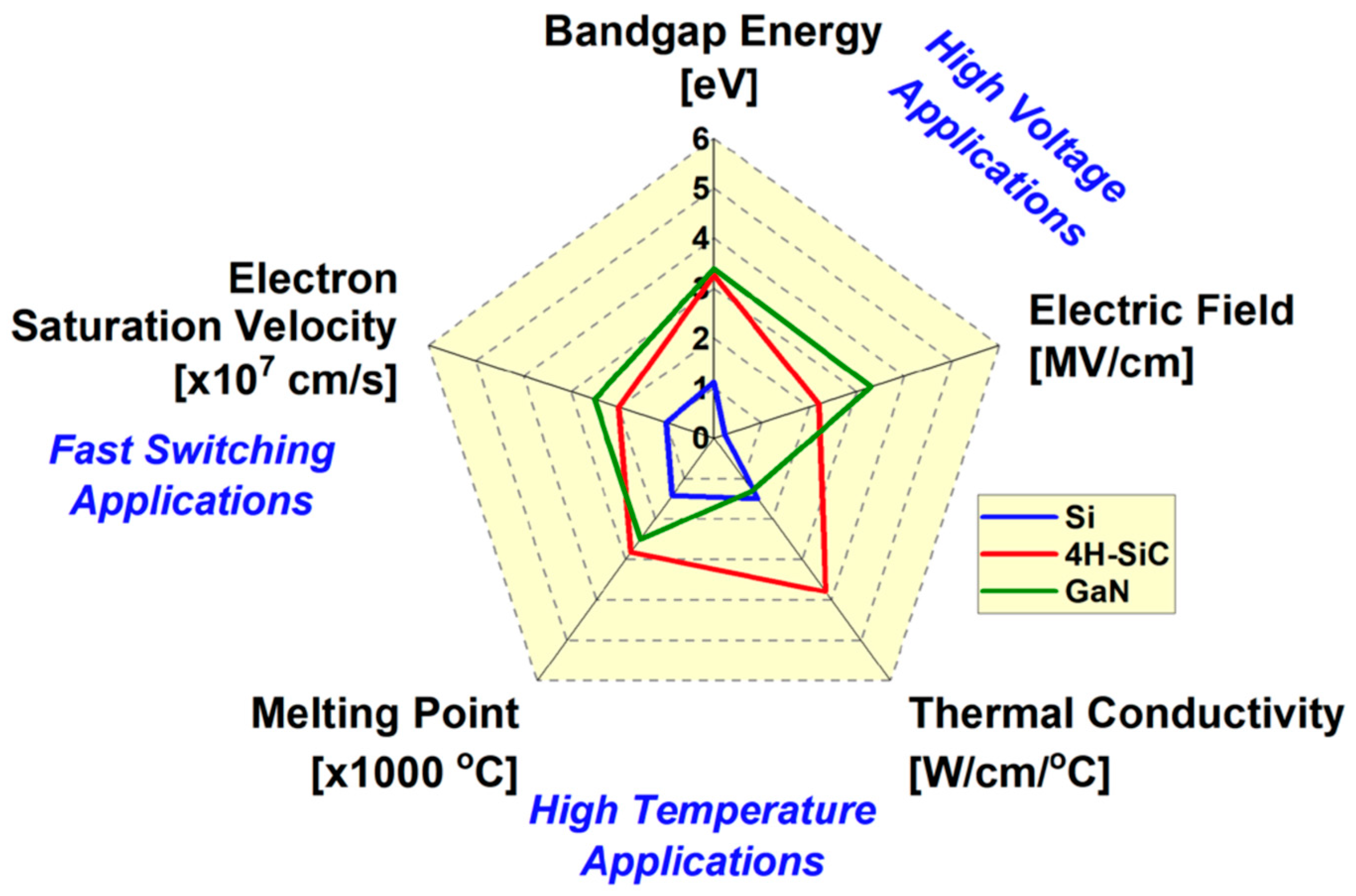
:1. Introduction
Motivation and Objective
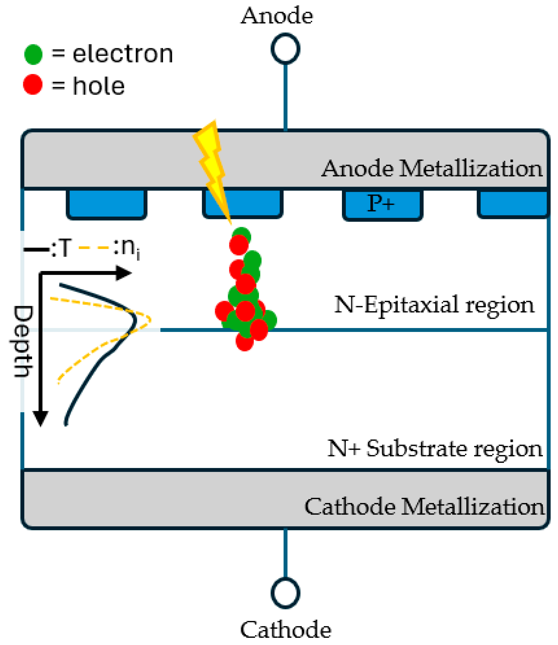
2. Review of SEB Failure Mechanisms
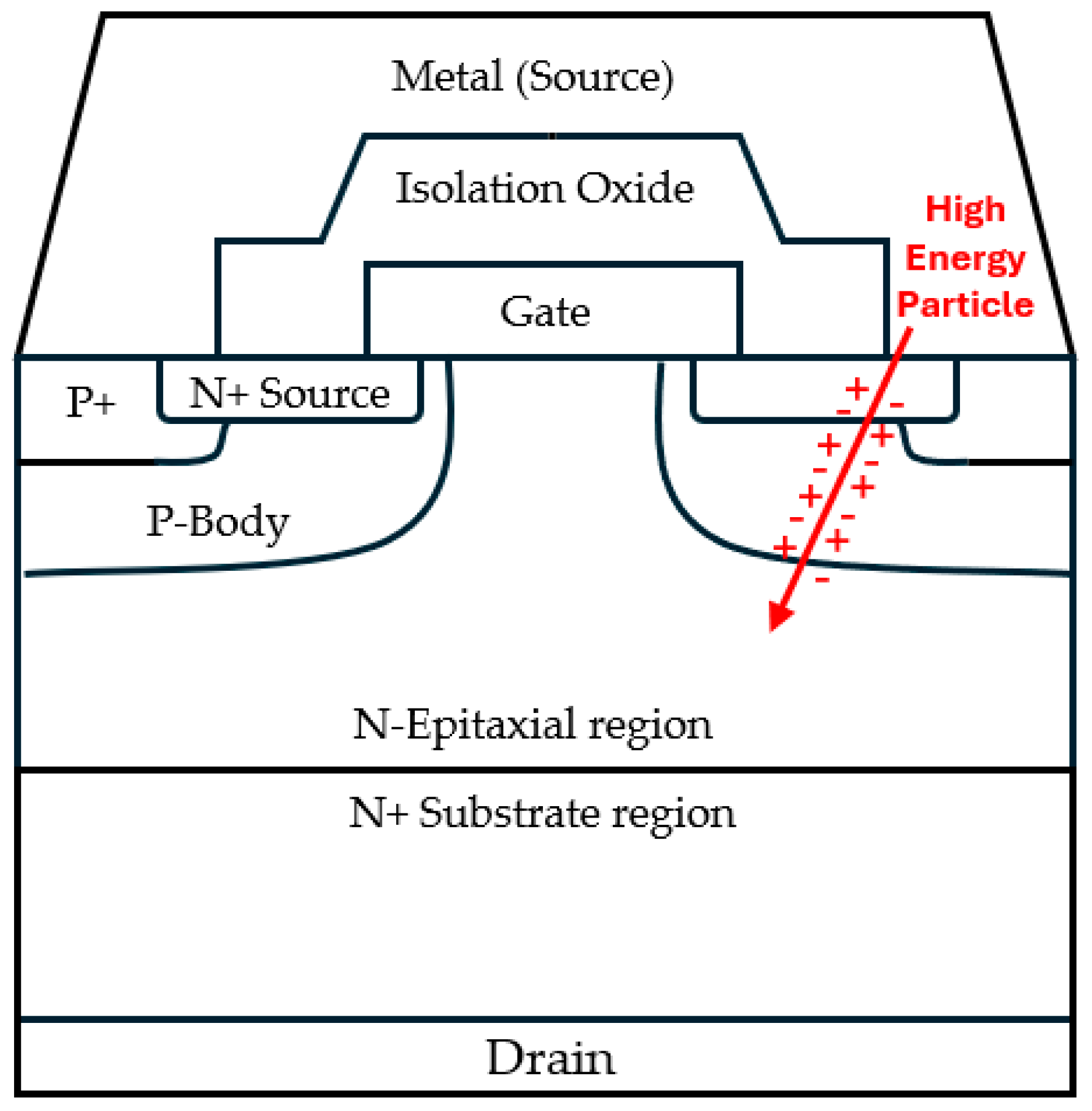
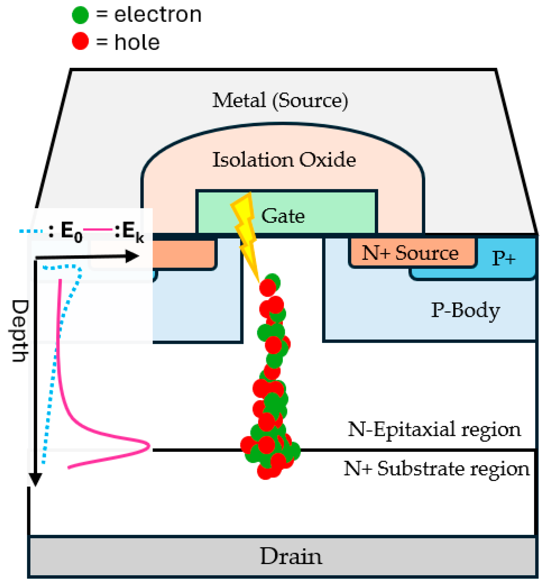
2.1. Evidence of the BJT Turn-On in Si MOSFETs during SEB
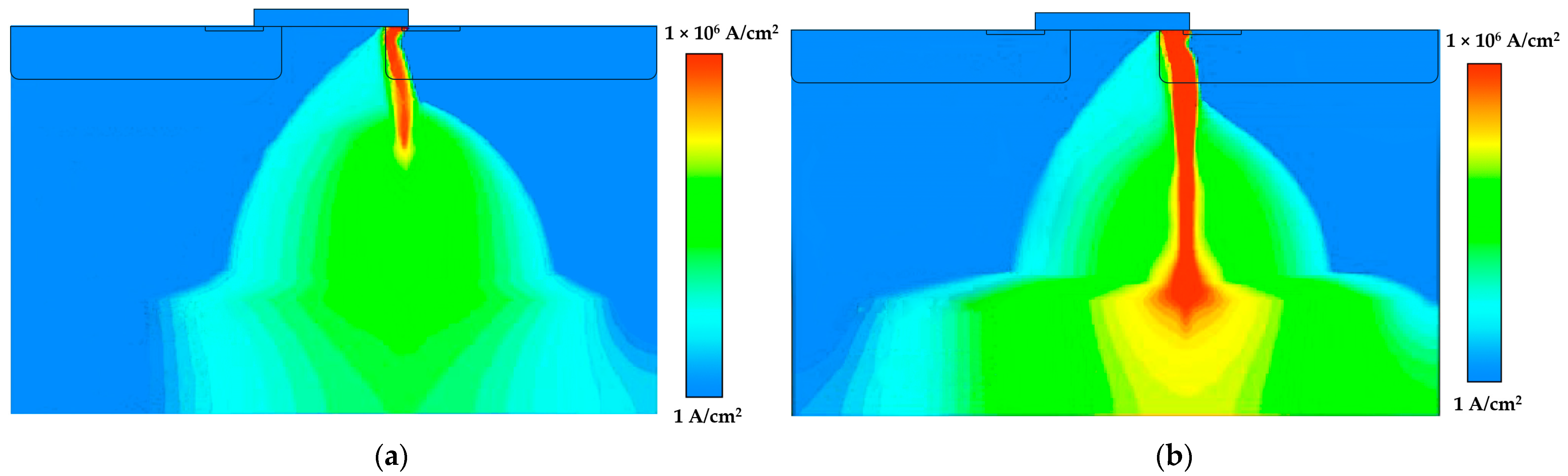
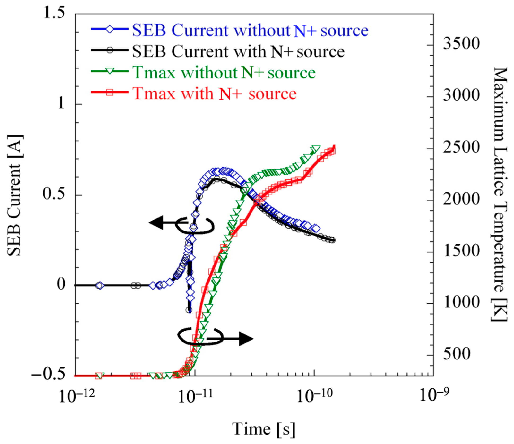
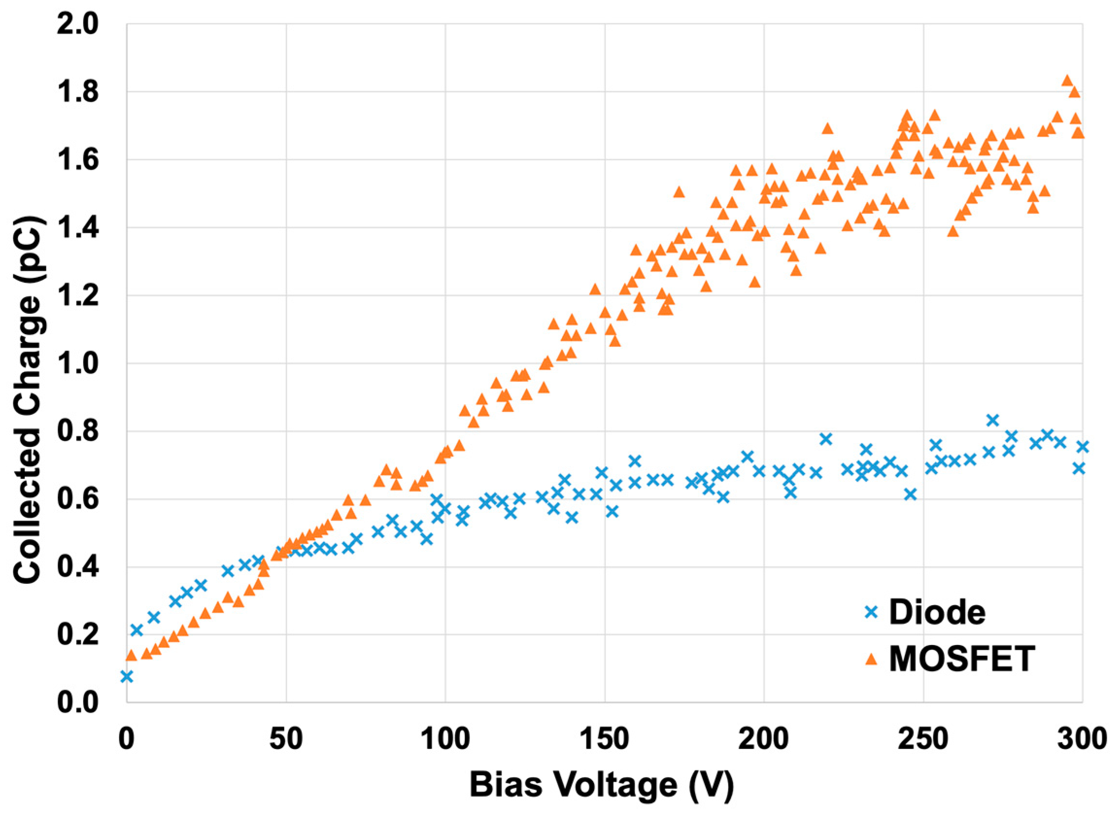
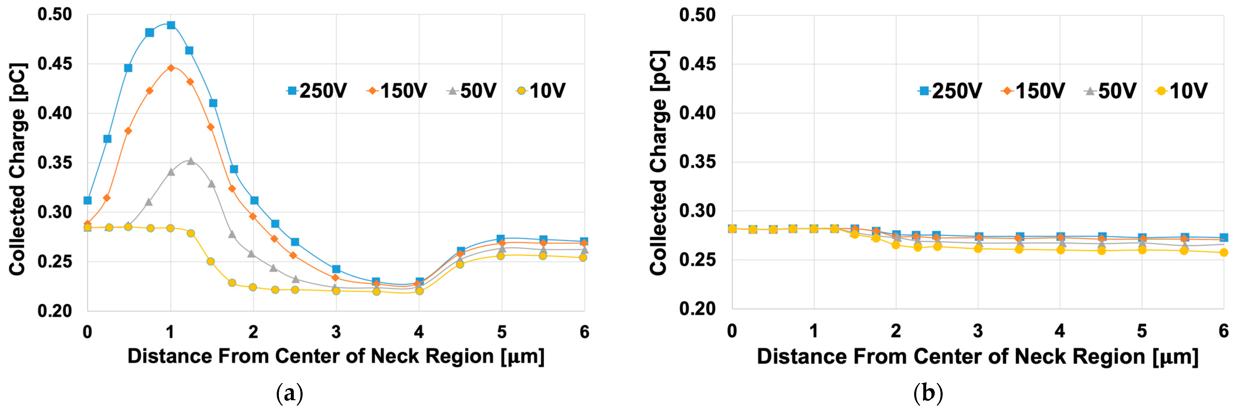
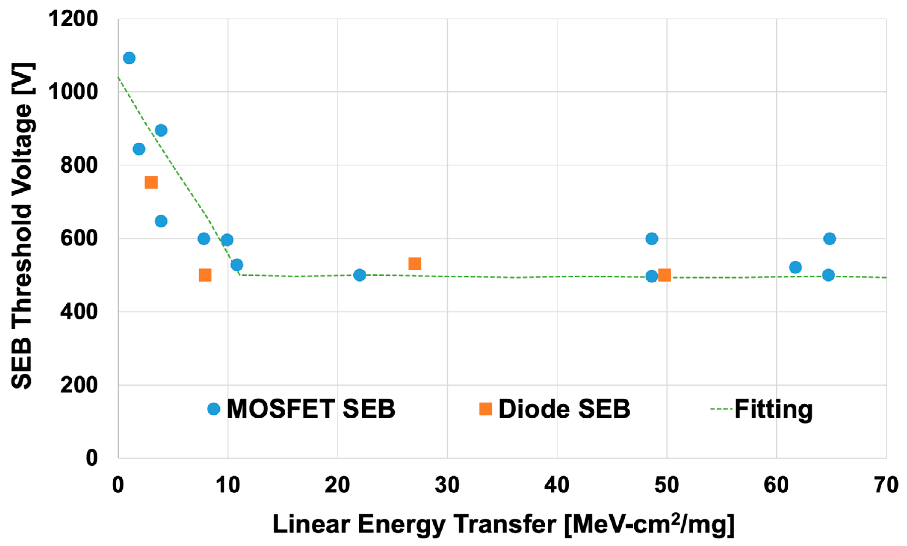
2.2. Review of SiC MOSFET SEB Failure Mechanisms
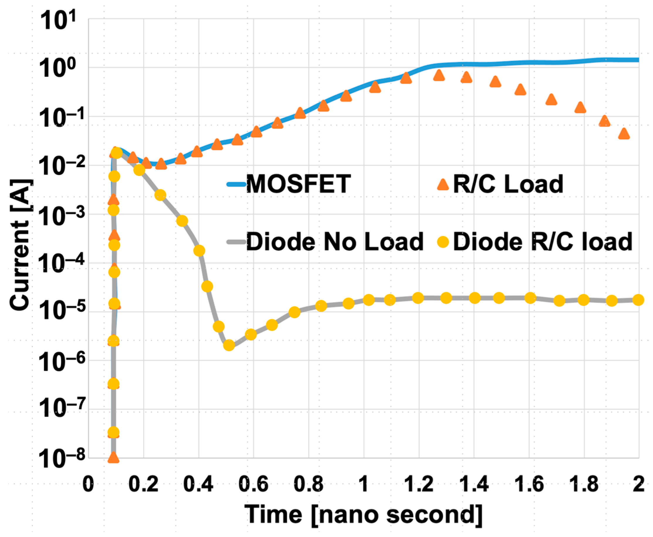
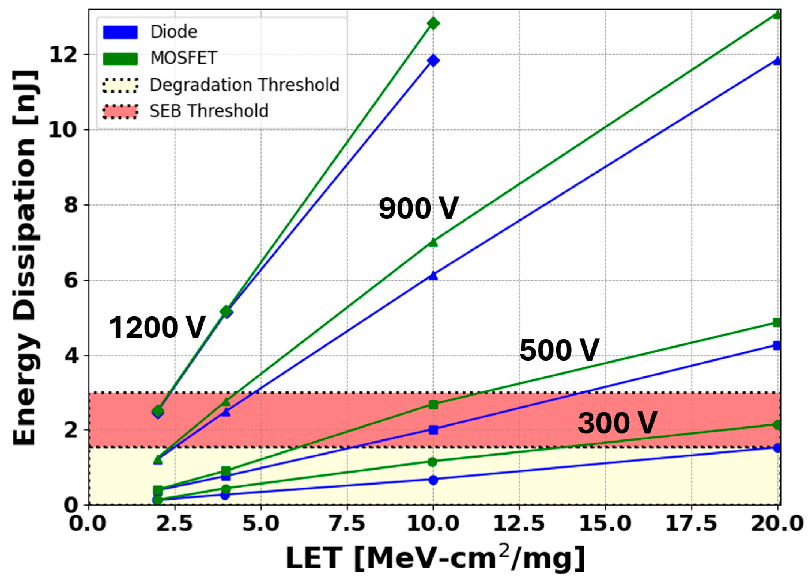
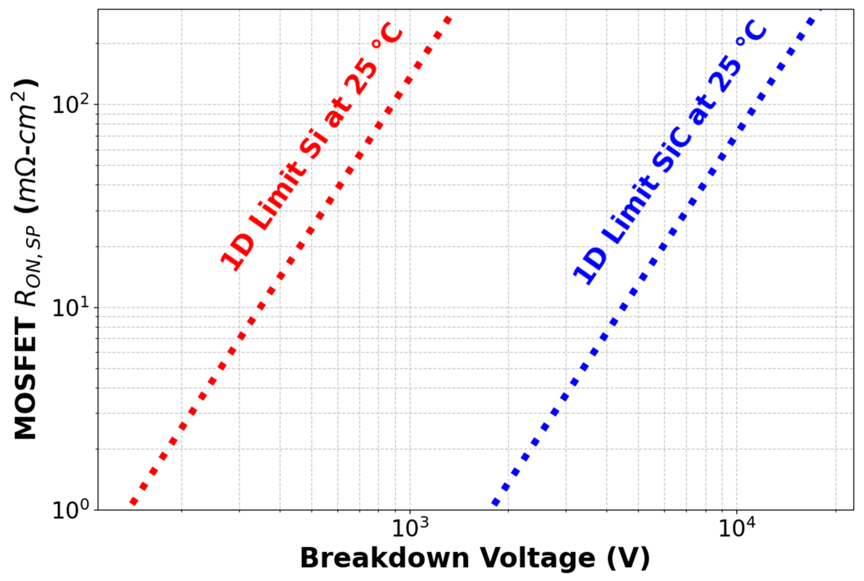
3. SEB Performance Review of Power Device Designs
3.1. Baseline VDMOSFET SEB Performance
Hardened VDMOSFET Designs
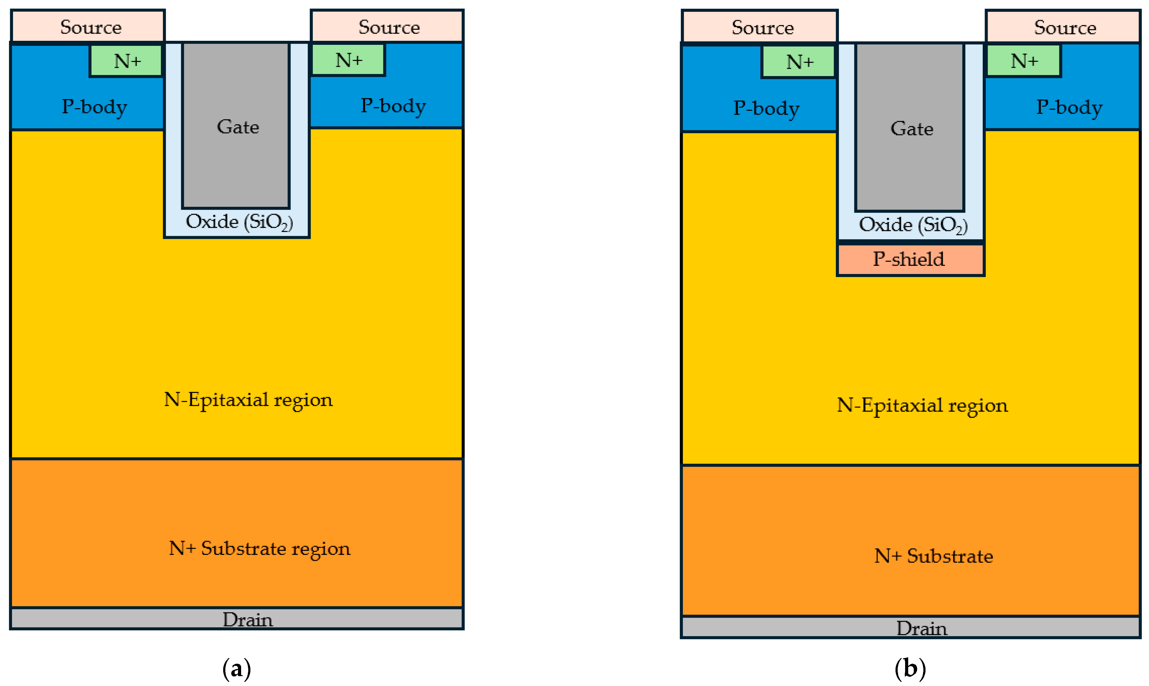
3.2. Baseline Trench Gate MOSFET SEB Performance
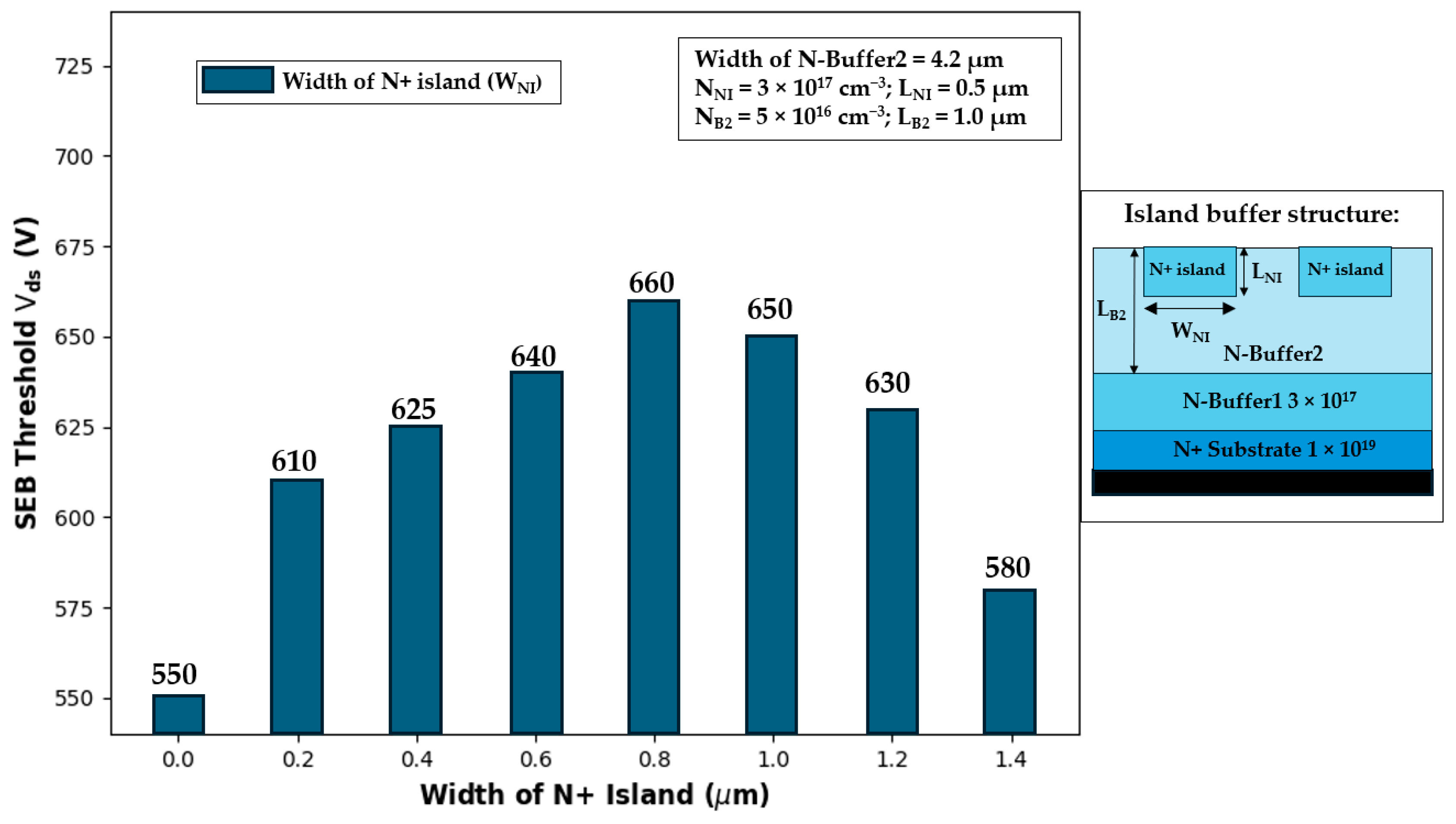
Hardened Trench Gate MOSFET Designs
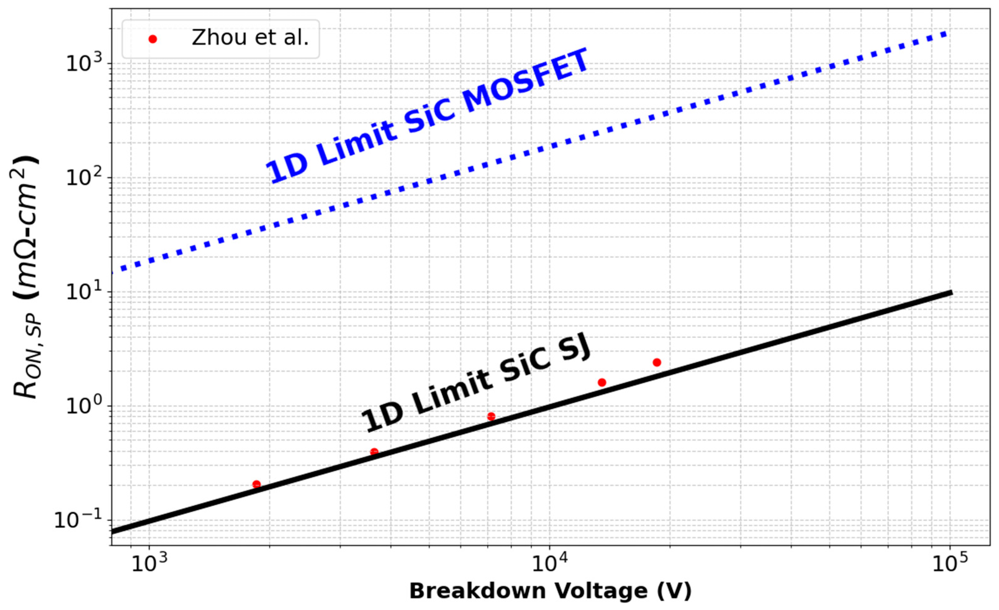
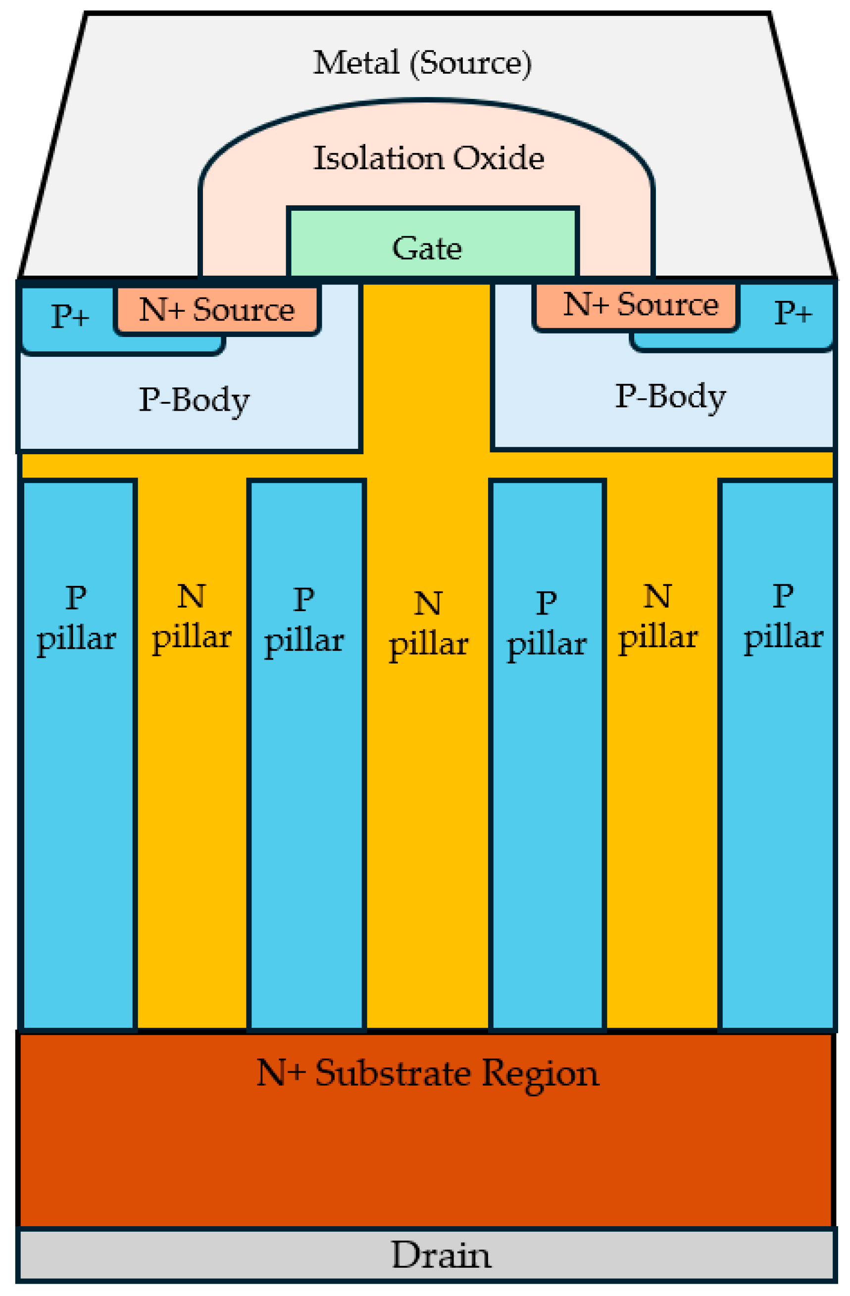
3.3. Baseline Superjunction MOSFET SEB Performance
Hardened Superjunction MOSFET Designs
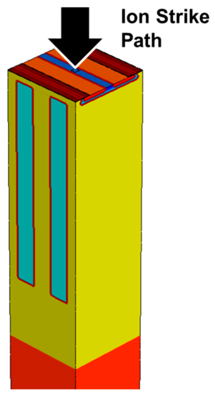
4. High-Fidelity Simulation
Single Event Burnout Criteria
5. Conclusions
Author Contributions
Funding
Data Availability Statement
Acknowledgments
Conflicts of Interest
References
- Lauenstein, J.-M. Wide-bandgap-power-SiC and GaN-radiation reliability. In Proceedings of the IEEE Nuclear and Space Radiation Effects Conference, Santa Fe, NM, USA, 29 November–30 December 2020. [Google Scholar]
- Tsao, J.Y.; Chowdhury, S.; Hollis, M.A.; Jena, D.; Johnson, N.M.; Jones, K.A.; Kaplar, R.J.; Rajan, S.; Van de Walle, C.G.; Bellotti, C.L.; et al. Ultrawide-Bandgap Semiconductors: Research Opportunities and Challenges. Adv. Electron. Mater. 2018, 4, 1600501. [Google Scholar] [CrossRef]
- NASA. Technology Roadmaps—TA 3: Space Power and Energy Storage. NASA Technol. Roadmaps 2020, 117–121, 158–165. [Google Scholar]
- Zhu, L. Design, Modeling, Fabrication and Characterization of Advanced High-Voltage 4H-Silicon Carbide Schottky Rectifiers. Ph. D. Thesis, Rensselaer Polytechnic Institute, Troy, NY, USA, 2005.
- Kimoto, T.; Cooper, J.A. Fundamentals of Silicon Carbide Technology: Growth, Characterization, Devices and Applications; John Wiley & Sons: Kyoto, Japan, 2014. [Google Scholar]
- Shaddock, D.; Meyer, L.; Tucker, J.; Dasgupta, S.; Fillion, R.; Bronecke, P.; Yorinks, L.; Kraft, P. Advanced materials and structures for high power wide bandgap devices. In Proceedings of the Ninteenth Annual IEEE Semiconductor Thermal Measurement and Management Symposium, San Jose, CA, USA, 11–13 March 2003. [Google Scholar]
- Nitta, T.; Sakiyama, Y.; Kotani, R.; Inoue, T.; Ohara, R.; Sano, K.; Yamaguchi, M.; Tchouangue, G. Cosmic Ray Failure Mechanism and Critical Factors for 3.3kV Hybrid SiC Modules. In Proceedings of the PCIM Europe 2016; International Exhibition and Conference for Power Electronics, Intelligent Motion, Renewable Energy and Energy Management, Nuremberg, Germany, 10–12 May 2016. [Google Scholar]
- Witulski, A.F.; Ball, D.R.; Galloway, K.F.; Javanainen, A.; Lauenstein, J.-M.; Sternberg, A.L.; Schrimpft, R.D. Single-Event Burnout Mechanisms in SiC Power MOSFETs. IEEE Trans. Nucl. Sci. 2018, 65, 1951–1955. [Google Scholar] [CrossRef]
- Zhu, X.; Lauenstein, J.-M.; Bolonikov, A.; Jacob, B.; Kashyap, A.; Sariri, K.; Chen, Y. Radiation hardness study on SiC power MOSFETs. In Proceedings of the International Conference on Silicon Carbide and Related Materials, Birmingham, UK, 2–6 September 2018. [Google Scholar]
- Shoji, T.; Nishida, S.; Hamada, K.; Tadano, H. Experimental and simulation studies of neutron-induced single-event burnout in SiC power diodes. Jpn. J. Appl. Phys. 2014, 53, 04EP03. [Google Scholar] [CrossRef]
- Lichtenwater, D.J.; Kaindl, W.; Treu, M.; Peters, D. Reliability of SiC Power Devices against Cosmic Ray Neutron Single-Event Burnout. Mater. Sci. Forum 2018, 924, 559–562. [Google Scholar] [CrossRef]
- Lauenstein, J.-M.; Casey, M. Taking SiC Power Devices to the Final Frontier: Addressing Challenges of the Space Radiation Environment; No. GSFC-E-DAA-TN47451; NASA Goddard Space Flight Center: Greenbelt, MD, USA, 2017.
- Titus, J.L.; Johnson, G.H.; Schrimpf, R.D.; Galloway, K.F. Single-event burnout of power bipolar junction transistors. IEEE Trans. Nucl. Sci. 1991, 38, 1315–1322. [Google Scholar] [CrossRef]
- Johnson, G.H. Features of a Heavy-Ion-Generated-Current Filament Used in Modeling Single-Event Burnout of Power MOSFETs. Master’s Thesis, University of Arizona, Tucson, AZ, USA, 1990. [Google Scholar]
- Hohl, J.H.; Johnson, G.H. Features of the triggering mechanism for single event burnout of power MOSFETs. IEEE Trans. Nucl. Sci. 1989, 36, 2260–2266. [Google Scholar] [CrossRef]
- Waskiewicz, J.W.; Groninger, J.W.; Strahan, V.H.; Long, D.M. Burnout of Power MOS Transistors with Heavy Ions of 252-Cf. IEEE Trans. Nucl. Sci. 1986, 33, 1710–1713. [Google Scholar] [CrossRef]
- Kuboyama, S.; Matsuda, S.; Kanno, T.; Ishii, T. Mechanism for single-event burnout of power MOSFETs and its characterization technique. IEEE Trans. Nucl. Sci. 1993, 39, 1698–1703. [Google Scholar] [CrossRef]
- Kuboyama, S.; Matsuda, S.; Nakajima, M.; Kanno, T.; Ishii, T. Numerical analysis of single event burnout of power MOSFETs. IEEE Trans. Nucl. Sci. 1993, 40, 1872–1879. [Google Scholar] [CrossRef]
- Casey, M.C.; Lauenstein, J.-M.; Ladbury, R.L.; Wilcox, E.P.; Topper, A.D.; LaBel, K.A. Schottky Diode Derating for Survivability in a Heavy-Ion Environment. IEEE Trans. Nucl. Sci. 2015, 62, 2482–2489. [Google Scholar] [CrossRef]
- Ball, D.R.; Galloway, K.F.; Johnson, R.A.; Alles, M.L.; Sternberg, A.L.; Sierawski, B.D.; Witulski, A.F. Ion-Induced Energy Pulse Mechanism for Single-Event Burnout in High-Voltage SiC Power MOSFETs and Junction Barrier Schottky Diodes. IEEE Trans. Nucl. Sci. 2020, 67, 22–28. [Google Scholar] [CrossRef]
- Lauenstein, J.-M.; Casey, M.C.; LaBel, K.A.; Topper, A.D.; Wilcox, E.P.; Kim, H.; Phan, A.M. Single-Event Effects in Silicon and Silicon Carbide Power Devices. In Proceedings of the NEPP Electronic Technology Workshop, Greenbelt, MD, USA, 17–19 June 2014. [Google Scholar]
- Shoji, T.; Nishida, S.; Hamada, K.; Tadano, H. Analysis of neutron induced single-event burnout in SiC power MOSFETs. Microelectron. Reliab. 2015, 55, 1517–1521. [Google Scholar] [CrossRef]
- Zhang, X. Failure Mechanism Investigation for Silicon Carbide Power Devices. Ph.D. Thesis, University of Maryland, College Park, MD, USA, 2006. [Google Scholar]
- Griffoni, A.; van Duivenbode, J.; Linten, D.; Simoen, E.; Rech, P.; Dilillo, L.; Wrobel, F.; Verbist, P.; Groeseneken, G. Neutron-induced failure in super-junction, IGBT, and SiC power devices. In Proceedings of the 12th European Conference on Radiation and Its Effects on Components and Systems, Sevilla, Spain, 19–23 September 2011. [Google Scholar]
- Johnson, R.A.; Witulski, A.F.; Ball, D.R.; Galloway, K.F.; Sternberg, A.L.; Zhang, E.; Ryder, L.D.; Reed, R.A.; Schrimpf, R.D.; Kozub, J.A.; et al. Enhanced charge collection in SiC power MOSFETs demonstrated by pulse-laser two-photon absorption SEE experiments. IEEE Trans. Nucl. Sci. 2019, 66, 1694–1701. [Google Scholar] [CrossRef]
- Zhou, X.; Jia, Y.; Hu, D.; Wu, Y. A simulation-based comparison between Si and SiC MOSFETs on single-event burnout susceptibility. IEEE Trans. Electron Devices 2019, 66, 2551–2556. [Google Scholar] [CrossRef]
- McPherson, J.A. Modeling and Improving Single-Event Burnout Performance from Heavy Ion Bombardment in High-Voltage 4h-SiC Power Devices. Ph.D. Thesis, Rensselaer Polytechnic Institute, Troy, NY, USA, 2021. [Google Scholar]
- McPherson, J.A.; Hitchcock, C.W.; Chow, T.P.; Ji, W.; Woodworth, A.A. Mechanisms of Heavy Ion-Induced Single Event Burnout in 4H-SiC Power MOSFETs. Mater. Sci. Forum 2020, 1004, 889–896. [Google Scholar] [CrossRef]
- McPherson, J.A.; Hitchcock, C.W.; Chow, T.P.; Ji, W.; Woodworth, A.A. Ion-Induced Mesoplasma Formation and Thermal Destruction in 4HSiC Power MOSFET Devices. IEEE Trans. Nucl. Sci. 2021, 68, 651–658. [Google Scholar] [CrossRef]
- Pocaterra, M.; Ciappa, M. Single event burnout failures caused in silicon carbide power devices by alpha particles emitted from radionuclides. E-Prime-Adv. Electr. Eng. Electron. Energy 2023, 5, 100203. [Google Scholar] [CrossRef]
- Zhang, H.; Guo, H.; Lei, Z.; Peng, C.; Zhang, Z.; Chen, Z.; Sun, C.; He, Y.; Zhang, F.; Pan, X.; et al. Experiment and simulation on degradation and burnout mechanisms of SiC MOSFET under heavy ion irradiation. Chin. Phys. B 2023, 32, 028504. [Google Scholar] [CrossRef]
- Kabza, H.; Schulze, H.J.; Gerstenmaier, Y.; Voss, P.; Schmid, J.W.W.; Pfirsch, F.; Platzoder, K. Cosmic radiation as a cause for power device failure and possible counter measures. In Proceedings of the 6th International Symposium on Power Semiconductor Devices and Ics, Davos, Switzerland, 31 May–2 June 1994. [Google Scholar]
- Kuboyama, S.; Ikeda, N.; Hirao, T.; Matsuda, S. Improved model for single-event burnout mechanism. IEEE Trans. Nucl. Sci. 2004, 51, 3336–3341. [Google Scholar] [CrossRef]
- Titus, J.L.; Jamiolkowski, L.S.; Wheatley, C.F. Development of cosmic ray hardened power MOSFETs. IEEE Trans. Nucl. Sci. 1989, 36, 2375–2382. [Google Scholar] [CrossRef]
- Kuboyama, S.; Sugimoto, K.; Shugyo, S.; Matsuda, S.; Hirao, T. Single-event burnout of epitaxial bipolar transistors. IEEE Trans. Nucl. Sci. 1998, 45, 2527–2533. [Google Scholar] [CrossRef]
- Porzio, A.; Busatto, G.; Velardi, F.; Iannuzzo, F.; Sanseverino, A.; Curro, G. Experimental and 3D simulation study on the role of the parasitic BJT activation in SEB/SEGR of power MOSFET. In Proceedings of the 2005 8th European Conference on Radiation and Its Effects on Components and Systems, Cap d’Agde, France, 19–23 September 2005. [Google Scholar]
- Liu, S.; Boden, M.; Girdhar, D.A.; Titus, J.L. Single-event burnout and avalanche characteristics of power DMOSFETs. IEEE Trans. Nucl. Sci. 2006, 53, 3379–3385. [Google Scholar] [CrossRef]
- Liu, S.; Titus, J.L.; Boden, M. Effect of buffer layer on single-event burnout of power DMOSFETs. IEEE Trans. Nucl. Sci. 2007, 54, 2554–2560. [Google Scholar] [CrossRef]
- Dachs, C.; Roubaud, F.; Palau, J.M.; Bruguier, G.; Bruguier, G.; Gasiot, J.; Tastet, P. Evidence of the ion’s impact position effect on SEB in n-channel power MOSFETs. IEEE Trans. Nucl. Sci. 1994, 41, 2167–2171. [Google Scholar] [CrossRef]
- Titus, J.L.; Wheatley, C.F. Experimental Studies of Single-Event Gate Rupture and Burnout in Vertical Power MOSFETs. IEEE Trans. Nucl. Sci. 1996, 43, 533–545. [Google Scholar] [CrossRef]
- Johnson, G.H.; Palau, J.M.; Dachs, C.; Galloway, K.F.; Schrimpf, D. A Review of the Techniques Used for Modeling Single-Event Effects in Power MOSFETs. IEEE Trans. Nucl. Sci. 1996, 43, 546–569. [Google Scholar] [CrossRef]
- Oberg, D.L.; Wert, J.L. First nondestructive measurements of power MOSFET single event burnout cross sections. IEEE Trans. Nucl. Sci. 1987, 34, 1736–1741. [Google Scholar] [CrossRef]
- Fischer, T.A. Heavy-ion-induced gate rupture in power MOSFETS. IEEE Trans. Nucl. Sci. 1987, 34, 1786–1791. [Google Scholar] [CrossRef]
- Titus, J.L. An updated perspective of single event gate rupture and single event burnout in power MOSFETs. IEEE Trans. Nucl. Sci. 2013, 60, 1912–1928. [Google Scholar] [CrossRef]
- Zeller, H.R. Cosmic ray induced breakdown in high voltages semiconductor devices, microscopic model and phenomenological lifetime prediction. In Proceedings of the Proceedings of the 6th International Symposium on Power Semiconductor Devices and Ics, Davos, Switzerland, 31 May–2 June 1994. [Google Scholar]
- Soelkner, G.; Voss, P.; Kaindl, W.; Wachutka, G.; Maier, K.H.; Becker, H.W. Charge carrier avalanche multiplication in high-voltage diodes triggered by ionizing radiation. IEEE Trans. Nucl. Sci. 2000, 47, 2365–2372. [Google Scholar] [CrossRef]
- Maier, K.H.; Denker, A.; Voss, P.; Becker, H.W. Single-event burnout in high power diodes. Nucl. Instrum. Amd Methods Phys. Res. Sect. B 1998, 146, 596–600. [Google Scholar] [CrossRef]
- Weiß, C.; Aschauer, S.; Wachutka, G.; Härtl, A.; Hille, F.; Pfirsch, F. Numerical analysis of cosmic radiation-induced failures in power diodes. In Proceedings of the European Solid-state Devices and Circuits Conference, Helsinki, Finland, 12–16 September 2011. [Google Scholar]
- O’Bryan, M.V.; LaBel, K.A.; Pellish, J.A.; Lauenstein, J.-M.; Chen, D.; Marshall, C.; Casey, M.C.; Sanders, A.B.; Ladbury, R.L.; Butte, A.J.; et al. Compendium of single event effects for candidate spacecraft electronics for NASA. In Proceedings of the 2012 Nuclear and Space Radiation Effects Conference (NSREC), Miami, FL, USA, 16–20 July 2012. [Google Scholar]
- Baliga, J.B. Fundamentals of Power Semiconductor Devices; Springer Science & Business Media: Berlin/Heidelberg, Germany, 2010. [Google Scholar]
- Selberherr, S. Analysis and Simulation of Seminconductor Devices; Springer: Verlan/Wien, Austria, 1984. [Google Scholar]
- Synopsys. Sentaurus Device User Guide; Synopsys: Mountain View, CA, USA, 2017. [Google Scholar]
- Kirk, C.T. A theory of transistor cut-off frequency (f) falloff at high current densities. IRE Trans. Electron Devices 1962, 9, 164–174. [Google Scholar] [CrossRef]
- Johnson, G.H.; Hohl, J.H.; Schrimpf, R.D.; Galloway, K.F. Simulating single event burnout of N-channel power MOSFET’s. IEEE Trans. Nucl. Sci. 1993, 40, 1001–1008. [Google Scholar] [CrossRef]
- Luu, A.; Patrick, A.; Miller, F.; Buard, N.; Carrière, T.; Poirot, P.; Gaillard, R.; Bafleur, M. Sensitive volume and triggering criteria of SEB in classic planar VDMOS. IEEE Trans. Nucl. Sci. 2010, 57, 1900–1907. [Google Scholar] [CrossRef]
- Javanainenm, A.; Galloway, K.F.; Nicklaw, C.; Bosser, A.L.; Ferlet-Cavrois, V.; Lauenstein, J.-M.; Pintacuda, F.; Reed, R.A.; Schrimpf, R.D.; Weller, R.A.; et al. Heavy Ion Induced Degradation in SiC Schottky Diodes: Bias and Energy Deposition Dependence. IEEE Trans. Nucl. Sci. 2017, 64, 415–420. [Google Scholar] [CrossRef]
- Witulski, A.F.; Arslanbekov, R.; Raman, A.; Schrimpf, R.D.; Sternberg, A.L.; Galloway, K.F.; Javanainen, A.; Grider, D.; Lichtenwater, D.J.; Hull, B. Single-Event Burnout of SiC Junction Barrier Schottky Diode High-Voltage Power Devices. IEEE Trans. Nucl. Sci. 2018, 65, 256–261. [Google Scholar] [CrossRef]
- Albadri, A.M.; Schrimpf, R.D.; Galloway, K.F.; Walker, D.G. Single event burnout in power diodes: Mechanisms and models. Microelectron. Reliab. 2006, 46, 317–325. [Google Scholar] [CrossRef]
- Mizuta, E.; Kuboyama, S.; Abe, H.; Iawata, Y.; Tamura, T. Investigation of Single-Event Damages on Silicon Carbide (SiC) Power MOSFETs. IEEE Trans. Nucl. Sci. 2014, 61, 1924–1928. [Google Scholar] [CrossRef]
- Li, P.; Zeng, L.; Li, X.; Luo, L.; Zhang, H.; Bo, M.; Sun, Y.; Yu, Q.; Tang, M.; Xu, W.; et al. Analysis of the influence of single event effects on the characteristics for SiC power MOSFETs. In Proceedings of the 2017 Prognostics and System Health Management Conference (PHM-Harbin), Harbin, China, 9–12 July 2017. [Google Scholar]
- Lauenstein, J.-M.; Casey, M.C.; Wilcox, E.P.; Kim, H.; Topper, A.D. Single-Event Effect Testing of the CREE C4D40120D Commercial 1200v Silicon Carbide Schottky Diode; NASA Goddard Space Flight Center: Greenbelt, MD, USA, 2014.
- McPherson, J.A.; Woodworth, A.A.; Chow, T.P.; Ji, W. Simulation-based study of single-event burnout in 4H-SiC high-voltage vertical super junction DMOSFET: Physical failure mechanism and robustness vs performance tradeoffs. Appl. Phys. Lett. 2022, 120, 043501. [Google Scholar] [CrossRef]
- Cheng, Y.Z.; Wang, Y.; Wu, X.; Cao, F. 4H-SiC UMOSFET With an Electric Field Modulation Region Below P-Body. IEEE Trans. Electron Devices 2020, 67, 3298–3303. [Google Scholar] [CrossRef]
- Yu, C.H.; Wang, Y.; Bao, M.T.; Li, X.J.; Yang, J.Q.; Tang, Z.H. Simulation Study on Single-Event Burnout in Rated 1.2-kV 4H-SiC Super-Junction VDMOS. IEEE Trans. Electron Devices 2021, 68, 5034–5040. [Google Scholar] [CrossRef]
- Gajewski, D.A.; Hull, B.; Lichtenwater, D.J.; Ryu, S.H.; Bonelli, E.; Mustain, H.; Wang, G.; Allen, S.T.; Palmour, J.W. SiC Power Device Reliability. In Proceedings of the 2016 IEEE International Integrated Reliability Workshop (IIRW), South Lake Tahoe, CA, USA, 9–13 October 2016. [Google Scholar]
- Liu, Q.; Wang, Q.; Liu, H.; Fei, C.; Li, S.; Huang, R.; Bai, S. Low on-resistance 1.2 kV 4H-SiC power MOSFET with Ron, sp of 3.4 m·cm2. J. Semicond. 2020, 41, 062801. [Google Scholar] [CrossRef]
- Ball, D.R.; Johnson, K.F.; Alles, R.A.; Sternberg, A.L.; Witulski, A.F.; Reed, R.A.; Schrimpf, R.D.; Hutson, J.M.; Lauenstein, J.-M. Effects of Breakdown Voltage on Single-Event Burnout Tolerance of High-Voltage SiC Power MOSFETs. IEEE Trans. Nucl. Sci. 2021, 68, 1430–1435. [Google Scholar] [CrossRef]
- Johnson, R.A.; Witulski, A.F.; Ball, D.R.; Galloway, K.F.; Sternberg, A.L.; Reed, R.A.; Schrimpf, R.D.; Alles, M.L.; Lauenstein, J.-M.; Javanainen, A.; et al. Unifying Concepts for Ion-Induced Leakage Current Degradation in Silicon Carbide Schottky Power Diodes. IEEE Trans. Nucl. Sci. 2020, 67, 135–139. [Google Scholar] [CrossRef]
- Lauenstein, J.-M.; Casey, M.C.; Ladbury, R.L.; Kim, H.S.; Phan, A.M.; Topper, A.D. Space radiation effects on SiC power device reliability. In Proceedings of the 2021 IEEE International Reliability Physics Symposium (IRPS), Monterey, CA, USA, 21–25 March 2021. [Google Scholar]
- Baumann, R.; Kruckmeyer, K. Radiation Handbook for Electronics; Texas Instruments: Dallas, TX, USA, 2020. [Google Scholar]
- Tawara, T.; Miyazawa, T.; Ryo, T.; Miyazato, M.; Fujimoto, T.; Takenaka, K.; Matsunaga, S.; Miyajima, M.; Otsuki, A.; Yonezawa, Y.; et al. Short minority carrier lifetimes in highly nitrogen doped 4H-SiC epilayers for suppression of the stacking fault formation in PiN diodes. J. Appl. Phys. 2016, 120, 115101. [Google Scholar] [CrossRef]
- Tawara, T.; Miyazawa, T.; Ryo, T.; Miyazato, M.; Fujimoto, T.; Takenaka, K.; Matsunaga, S.; Miyajima, M.; Otsuki, A.; Yonezawa, Y.; et al. Suppression of the forward degradation in 4H-SiC PiN diodes by employing a recombination-enhanced buffer layer. Mater. Sci. Forum 2017, 897, 419–422. [Google Scholar] [CrossRef]
- Lu, J.; Liu, J.; Tian, X.; Chen, H.; Tang, Y.; Bai, Y.; Li, C.; Liu, X. Impact of Varied Buffer Layer Designs on Single-Event Response of 1.2-kV SiC Power MOSFETs. IEEE Trans. Electron Devices 2020, 67, 3698–3704. [Google Scholar] [CrossRef]
- Boige, F.; Rchardeau, F.; Lefebvre, S.; Blaquière, J.M.; Guibaud, G.; Bourennane, A. Ensure an original and safe ‘fail-to-open’ mode in planar and trench power SiC MOSFET devices in extreme shortcircuit operation. Microelectron. Reliab. 2018, 88, 598–603. [Google Scholar] [CrossRef]
- Nakamura, T.; Nakano, Y.; Aketa, M.; Nakamura, R.; Mitani, S.; Sakairi, H.; Yokotsuji, Y. High performance SiC trench devices with ultra-low Ron. In Proceeding of the IEEE International Electron Devices Meeting (IEDM), Washington, DC, USA, 5–7 December 2011. [Google Scholar]
- Zhou, X.; Tang, Y.; Jia, Y.; Hu, D.; Wu, Y.; Xia, T.; Gong, H.; Pang, H. Single-Event Effects in SiC Double-Trench MOSFETs. IEEE Trans. Nucl. Sci. 2019, 66, 2312–2318. [Google Scholar] [CrossRef]
- Yu, C.H.; Wang, Y.; Cao, F.; Huang, L.L.; Wang, Y.Y. Research of Single-Event Burnout in Power Planar VDMOSFETs by Localized Carrier Lifetime Control. IEEE Trans. Nucl. Sci. 2015, 62, 143–148. [Google Scholar]
- Ozpineci, B.; Tolbert, L.M. Comparison of Wide-Bandgap Semiconductors for Power Electronics Applications; Tech. Rep. ORNL/TM-2003/257; Oak Ridge National Lab: Oak Ridge, TN, USA, 2004. [Google Scholar]
- Lophitis, N.; Arvanitopoulos, A.; Perkins, S.; Antoniou, M.; Sharma, Y.K. TCAD Device Modelling and Simulation of Wide Bandgap Power Semiconductors. In Disruptive Wide Bandgap Semiconductors, Related Technologies, and Their Applications; Intech Open: Rijeka, Croatia, 2018. [Google Scholar]
- Peters, D.; Aichinger, T.; Basler, T.; Bergner, W.; Kueck, D.; Esteve, R. 1200V SiC Trench-MOSFET optimized for high reliability and high performance. Mater. Sci. Forum 2016, 897, 489–492. [Google Scholar] [CrossRef]
- Krishnamurthy, S.; Ramani, K.; Hussin, F.A. Single event burnout hardening of trench shielded power UMOSFET using High-k dielectrics. Mater. Res. Express 2020, 7, 035907. [Google Scholar] [CrossRef]
- Felix, J.A.; Shaneyfelt, M.R.; Schwank, J.R.; Dalton, S.M.; Dodd, P.E.; Witcher, J.B. Enhanced Degradation in Power MOSFET Devices Due to Heavy Ion Irradiation. IEEE Trans. Nucl. Sci. 2007, 54, 2181–2189. [Google Scholar] [CrossRef]
- Galloway, K.F. A Brief Review of Heavy-Ion Radiation Degradation and Failure of Silicon UMOS Power Transistors. Electronics 2014, 3, 582–593. [Google Scholar] [CrossRef]
- Kuboyama, S.; Maru, A.; Ikeda, N.; Hirao, T.; Tamura, T. Characterization of Microdose Damage Caused by Single Heavy Ion Observed in Trench Type Power MOSFETs. IEEE Trans. Nucl. Sci. 2010, 57, 3257–3261. [Google Scholar] [CrossRef]
- Liu, S.; Zafrani, M.; Cao, H.; Berberian, R.; DiCienzo, C.; Boden, M. Vulnerable Trench power MOSFETs under heavy ion irradiation. In Proceedings of the IEEE Nuclear and Space Radiation Effects Conference, Tucson, AZ, USA, 14–18 July 2008. [Google Scholar]
- Shaneyfelt, M.R.; Felix, J.A.; Dodd, P.E.; Schwank, J.R.; Dalton, S.M.; Baggio, J.; Ferlet-Cavrois, V.; Paillet, P.; Blackmore, E.W. Enhanced proton and neutron induced degradation and its impact on hardness assurance testing. IEEE Trans. Nucl. Sci. 2008, 55, 3096–3105. [Google Scholar] [CrossRef]
- Zebrev, G.I.; Vatuev, A.S.; Useinov, R.G.; Emeliyanov, V.V.; Anashin, V.S.; Gorbunov, M.S.; Turin, V.O.; Yesenkov, K.A. Microdose induced drain leakage effects in power trench MOSFETs: Experiment and modeling. IEEE Trans. Nucl. Sci. 2014, 61, 1531–1536. [Google Scholar] [CrossRef]
- Wan, X.; Zhou, W.; Liu, D.; Bo, H.; Xu, J. Charge deposition model for investigating SE-microdose effect in trench power MOSFETs. J. Semicond. 2015, 36, 54003. [Google Scholar] [CrossRef]
- Lauenstein, J.-M.; Casey, M.C.; Wilcox, E.P.; Phan, A.M.; Kim, H.S.; Topper, A.D.; Ladbury, R.L.; LaBel, K.A. Recent Radiation Test Results for Trench Power MOSFETs. In Proceedings of the 2017 IEEE Radiation Effects Data Workshop (REDW), New Orleans, LA, USA, 17-21 July 2017. [Google Scholar]
- Wang, L.; Jia, Y.; Zhou, X.; Zhao, Y.; Wang, L.; Li, T.; Hu, D.; Wu, Y.; Deng, Z. Heavy-ion induced gate damage and thermal destruction in double-trench SiC MOSFETs. Microelectron. Reliab. 2022, 137, 114770. [Google Scholar] [CrossRef]
- Kim, J.; Kim, K. Single-Event Burnout Hardening 4H-SiC UMOSFET Structure. IEEE Trans. Device Mater. Reliab. 2022, 22, 164–168. [Google Scholar] [CrossRef]
- Wang, Y.; Lin, M.; Li, X.J.; Wu, X.; Yang, J.Q.; Bao, M.T.; Yu, C.H.; Cao, F. Single-Event Burnout Hardness for the 4H-SiC Trench-Gate MOSFETs Based on the Multi-Island Buffer Layer. IEEE Trans. Electron Devices 2019, 66, 4264–4272. [Google Scholar] [CrossRef]
- Shen, P.; Wang, Y.; Li, X.; Yang, J.; Zheng, L. Simulation study on single-event burnout reliability of 4H-SiC trench gate MOSFET with combined P-buried layer. Mircoelectronics Reliab. 2023, 142, 114931. [Google Scholar] [CrossRef]
- Wang, Y.; Zhou, J.; Lin, M.; Li, X.; Yang, J.Q.; Cao, F. A Comparative Study of Single-Event-Burnout for 4H-SiC UMOSFET. IEEE Trans. Electron Devices 2022, 10, 373–378. [Google Scholar] [CrossRef]
- Wang, Y.; Ma, Y.C.; Hao, Y.; Hu, Y.; Wang, G.; Cao, F. Simulation study of 4H-SiC UMOSFET structure with p+−polySi/SiC shielded region. IEEE Trans. Electron Devices 2017, 64, 3719–3724. [Google Scholar] [CrossRef]
- Bi, J.; Wang, Y.; Wu, Y.; Li, X.; Yang, J.; Bao, M.T.; Cao, F. Single-Event Burnout Hardening Method and Evaluation in SiC Power MOSFET devices. IEEE Trans. Electron Devices 2020, 67, 4340–4345. [Google Scholar] [CrossRef]
- Tanaka, H.; Hayashi, T.; Shimoida, Y.; Yamagami, S.; Tanimoto, S.; Hoshi, M. Ultra-low von and high voltage 4H-SiC heterojunction diode. In Proceedings of the IEEE 17th International Symposium of Power Semiconductor ICs, Santa Barbara, CA, USA, 23–26 May 2005. [Google Scholar]
- Yasuhiko, O.; Hashimoto, Y. Numerical analysis of specific on-resistance for trench gate superjunction MOSFETs. Jpn. J. Appl. Phys. 2015, 54, 024101. [Google Scholar]
- Huang, S.; Amaratunga, G.A.J.; Udrea, F. Analysis of SEB and SEGR in super-junction MOSFETs. IEEE Trans. Nucl. Sci. 2000, 47, 2640–2647. [Google Scholar] [CrossRef]
- Ikeda, N.; Kuboyama, S.; Matsuda, S. Single-event burnout of Super-junction power MOSFETs. IEEE Trans. Nucl. Sci. 2004, 51, 3332–3335. [Google Scholar] [CrossRef]
- Wang, L.; Song, L.; Wang, L.; Li, B.; Luo, J.; Han, Z. A Novel Super-Junction Structure to Improve SEB Performance. In Proceedings of the 14th IEEE International Conference on Solid-State and Integrated Circuit Technology, Qingdao, China, 31 October–3 November 2018. [Google Scholar]
- Muthuseenu, K.; Barnaby, H.J.; Galloway, K.F.; Koziukov, A.E.; Maksimenko, T.A.; Vyrostkov, M.Y.; Bu-Khasan, K.B.; Kalashnikova, A.A.; Privat, A. Analysis of SEGR in Silicon Planar Gate Super-Junction Power MOSFETs. IEEE Trans. Nucl. Sci. 2021, 68, 611–616. [Google Scholar] [CrossRef]
- Katoh, S.; Shimada, E.; Yoshihira, T.; Oyama, A.; Ono, S.; Ura, H.; Ookura, G.; Saito, W.; Kawaguchi, Y. Temperature dependence of single-event burnout for super junction MOSFET. In Proceedings of the International Symposium on Power Semiconductor Devices & IC’s, Hong Kong, China, 10–14 May 2015. [Google Scholar]
- Zerarka, M.; Austin, P.; Morancho, F.; Isoird, K.; Arbess, H.; Tasselli, J. Analysis study of sensitive volume and triggering criteria of singleevent burnout in super-junction metal-oxide semiconductor field-effect transistors. IET Circuits Devices Syst. 2014, 8, 197–220. [Google Scholar] [CrossRef]
- Muthuseenu, K.; Barnaby, H.J.; Galloway, K.F.; Koziukov, A.E.; Maksimenko, T.A.; Vyrostkov, M.Y.; Bu-Khasan, K.B.; Kalashnikova, A.A.; Privat, A. Single-Event Gate Rupture Hardened Structure for High-Voltage Super-Junction Power MOSFETs. IEEE Trans. Electron Devices 2021, 68, 4004–4009. [Google Scholar] [CrossRef]
- Harada, S.; Kobayashi, Y.; Kyogoku, S.; Morimoto, T.; Tanaka, T.; Takei, M.; Okumura, H. First Demonstration of Dynamic Characteristics for SiC Superjunction MOSFET Realized using Multi-epitaxial Growth Method. In Proceedings of the IEEE International Electron Devices Meeting, San Francisco, CA, USA, 1–5 December 2018. [Google Scholar]
- Masuda, T.; Kosugi, R.; Hiyoshi, T. 97mΩ-cm2/820V 4H-SiC super junction V-groove trench MOSFET. Mater. Sci. Forum 2017, 897, 483–488. [Google Scholar] [CrossRef]
- Kang, H.; Udrea, F. True Material Limit of Power Devices—Applied to 2-D Superjunction MOSFET. IEEE Trans. Electron Devices 2018, 65, 1432–1439. [Google Scholar] [CrossRef]
- Zhou, X.; Guo, Z.B.; Chow, T.P. Performance limits of vertical 4H-SiC and 2H-GaN superjunction devices. Mater. Sci. Forum 2019, 963, 693–696. [Google Scholar] [CrossRef]
- McPherson, J.A.; Woodworth, A.A.; Chow, T.P.; Ji, W. Robustness of Semi-Superjunction 4H-SiC Power DMOSFETs to Single-Event Burnout from Heavy Ion Bombardment. Mater. Sci. Forum 2022, 1062, 683–687. [Google Scholar] [CrossRef]
- McPherson, J.A.; Kowal, P.J.; Pandey, G.K.; Chow, T.P.; Ji, W.; Woodworth, A.A. Heavy Ion Transport Modeling for Single-Event Burnout in SiC-Based Power Devices. IEEE Trans. Nucl. Sci. 2019, 66, 474–481. [Google Scholar] [CrossRef]
- Hatakeyama, T.; Ota, C.; Shinohe, T. Physical Modeling and Scaling Properties of 4H-SiC Power Devices. In Proceedings of the International Conference On Simulation of Semiconductor Processes and Devices, Tokyo, Japan, 1–3 September 2005. [Google Scholar]
- Niwa, H.; Suda, J.; Kimoto, T. Temperature Dependence of Impact Ionization Coefficients in 4H-SiC. Mater. Sci. Forum 2014, 778–780, 461–466. [Google Scholar] [CrossRef]
- Gupta, M.K.; Gupta, N. PN Junctions and Their Breakdown Mechanisms. In Advanced Semiconducting Materials and Devices; Springer: Berlin/Heidelberg, Germany, 2016. [Google Scholar]


| Device Type | LET (MeV-cm2/mg) | VSEB/VR | Ref. |
|---|---|---|---|
| MOSFET | 14 | 0.54 | [1] |
| JBS Diode | 59 | 0.75–1.0 | [19] |
| MOSFET with N+ source | 30 | 0.40–0.56 | [17] |
| MOSFET removed N+ source | 30 | >0.68 | [17] |
| No in-line resistor MOSFET | 12–15 | 0.40–0.50 | [42] |
| Resistor-protected MOSFET | 12–15 | 0.70–1.0 | [42] |
| Device Type | LET (MeV-cm2/mg) | VSEB/VR | Ref. |
|---|---|---|---|
| MOSFET | 24 | 0.50 | [1] |
| JBS Diode | 27 | 0.42 | [57] |
| No in-line resistor MOSFET | 22 | 0.42 | [20] |
| Resistor-protected MOSFET | 20 | 0.41 | [20] |
| BJT Turn-on Primary Mechanism 1 | Coupled BJT-Impact Ionization Mechanism 2 | Mesoplasma Formation Mechanism 3 | High-Energy Pulse Mechanism 4 | |
|---|---|---|---|---|
| Internal Carrier Generation | Injected carriers flow toward terminals, forward biases BJT | Injected carriers flow toward terminals, forward biases BJT | Mass carrier transit modulates E-field, initiates impact ionization | Resistive shunts cause increased current |
| Regenerative Feedback Mechanism | BJT turns on, begins regeneratively feeding current into device | BJT produces constant current. Peak E-field initiates impact ionization generation of carriers. | High carrier density heats device, thermally generating carriers leading to higher density. | Simultaneous high current and high voltage cause energy dissipation |
| Runaway Failure | Simultaneous high current and high voltage causes second breakdown and thermal runaway | Mass carrier multiplication leads to avalanche effect causing SEB | Regenerative carrier creation forms a self-sustained mesoplasma until sublimation of material | Energy pulses cumulate until surpassing device limit |
| Device Design | Study Type | LET (MeV-cm2/mg) | VSEB (V) | Ron,sp (mΩ-cm2) |
|---|---|---|---|---|
| [1200 V] DMOSFET 1 | Experiment | 10–65 | 500–600 | 2–3 |
| [3300 V] Derated DMOSFET 2 | Experiment | 60 | 825 | 10 |
| [3000 V] Derated DMOSFET 3 | 3D Simulation | 46 | 1200 | 7.6 |
| [1500 V] Buffer Layer DMOSFET 3 | 3D Simulation | 46 | 1200 | 3.2 |
| [1200 V] DMOSFET 4 | 3D Simulation | 46 | 525 | 3.7 |
| [1200 V] Non-uniform Buffer Layer DMOSFET 4 | 3D Simulation | 46 | 925 | 3.9 |
| [1200 V] Narrow-channel DMOSFET 5 | 2.5D Simulation * | 40 | 1000–1200 | N.A. |
| Device Design | Study Type | LET (MeV-cm2/mg) | VSEB (V) | Ron,sp (mΩ-cm2) |
|---|---|---|---|---|
| [1200 V] UMOSFET 1 | Experiment | 75 | 500 | 3.0–3.3 2,3 |
| [1200 V] UMOSFET 4 | 2D Simulation | 7.6 | 530 | 16.6 |
| [1200 V] SAS UMOSFET 4 | 2D Simulation | 7.6 | 660 | 16.6 |
| [3300 V] P-shield UMOSFET 5 | 2D Simulation | 75 | 900 | 9.4 |
| [3300 V] DGF UMOSFET 5 | 2D Simulation | 75 | 1500 | 5.5 |
| [900 V] Multi-buffer Layer UMOSFET 6 | 2D Simulation | 75 | 650 | 6.0 |
| [650 V] UMOSFET 7 | 2D Simulation | 75 | 71 | 1.9 |
| [650 V] Lmesa Adjusted UMOSFET 7 | 2D Simulation | 75 | 320 | 2.9 |
| Device Design | Study Type | LET (MeV-cm2/mg) | VSEB (V) | Ron,sp (mΩ-cm2) |
|---|---|---|---|---|
| [600 V] Si SJ MOSFET 1 | Experiment | 35 | 350 | N.A. |
| [5500 V] SiC SJ MOSFET 2 | 3D Simulation | 46 | 1150 | 3.0 |
| [650 V] Si SJ MOSFET 3 | 2D Simulation * | 151 | 103 | 7.5 |
| [1200 V] SiC SJ MOSFET 4 | 2D Simulation | 77.9 | 500 | 3.5 |
| [650 V] Si Graded Buffer Layer SJ 3 | 2D Simulation * | 151 | 695 | 10 |
| [4500 V] SiC Semi-SJ MOSFET 5 | 3D Simulation | 46 | 1750 | 3.2 |
| [1200 V] SiC Buffer Layer SJ MOSFET 4 | 2D Simulation | 77.9 | 800 | 3.9 |
Disclaimer/Publisher’s Note: The statements, opinions and data contained in all publications are solely those of the individual author(s) and contributor(s) and not of MDPI and/or the editor(s). MDPI and/or the editor(s) disclaim responsibility for any injury to people or property resulting from any ideas, methods, instructions or products referred to in the content. |
© 2024 by the authors. Licensee MDPI, Basel, Switzerland. This article is an open access article distributed under the terms and conditions of the Creative Commons Attribution (CC BY) license (https://creativecommons.org/licenses/by/4.0/).
Share and Cite
Grome, C.A.; Ji, W. A Brief Review of Single-Event Burnout Failure Mechanisms and Design Tolerances of Silicon Carbide Power MOSFETs. Electronics 2024, 13, 1414. https://doi.org/10.3390/electronics13081414
Grome CA, Ji W. A Brief Review of Single-Event Burnout Failure Mechanisms and Design Tolerances of Silicon Carbide Power MOSFETs. Electronics. 2024; 13(8):1414. https://doi.org/10.3390/electronics13081414
Chicago/Turabian StyleGrome, Christopher A., and Wei Ji. 2024. "A Brief Review of Single-Event Burnout Failure Mechanisms and Design Tolerances of Silicon Carbide Power MOSFETs" Electronics 13, no. 8: 1414. https://doi.org/10.3390/electronics13081414
APA StyleGrome, C. A., & Ji, W. (2024). A Brief Review of Single-Event Burnout Failure Mechanisms and Design Tolerances of Silicon Carbide Power MOSFETs. Electronics, 13(8), 1414. https://doi.org/10.3390/electronics13081414