
A New 1 Bit Electronically Reconfigurable Transmitarray

Abstract
:1. Introduction
2. Design and Optimization of Proposed Unit Cell
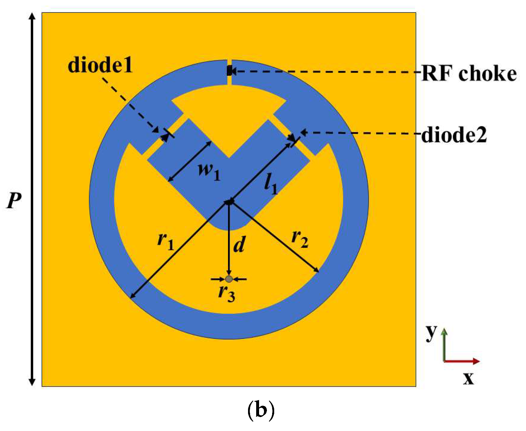
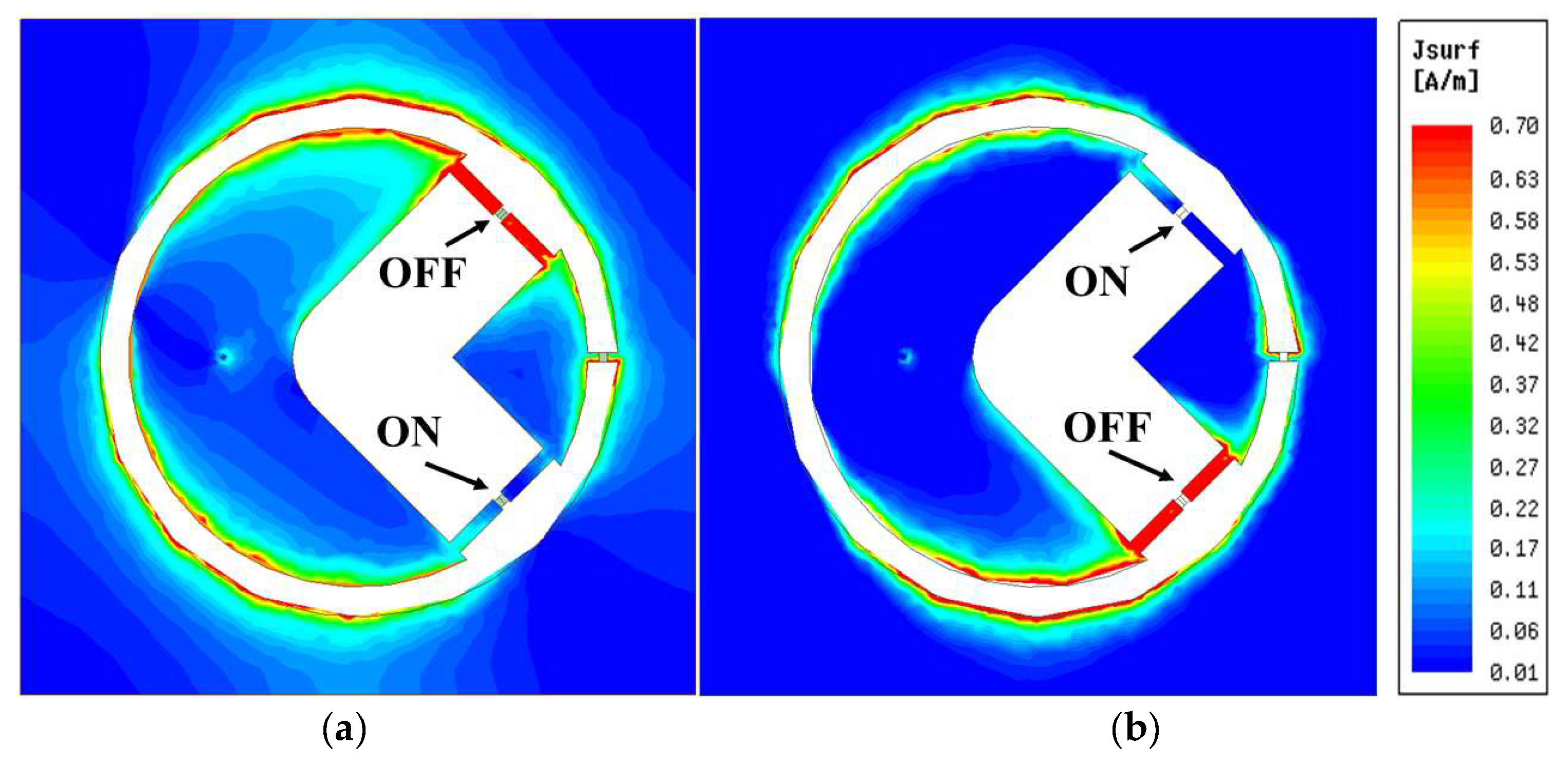
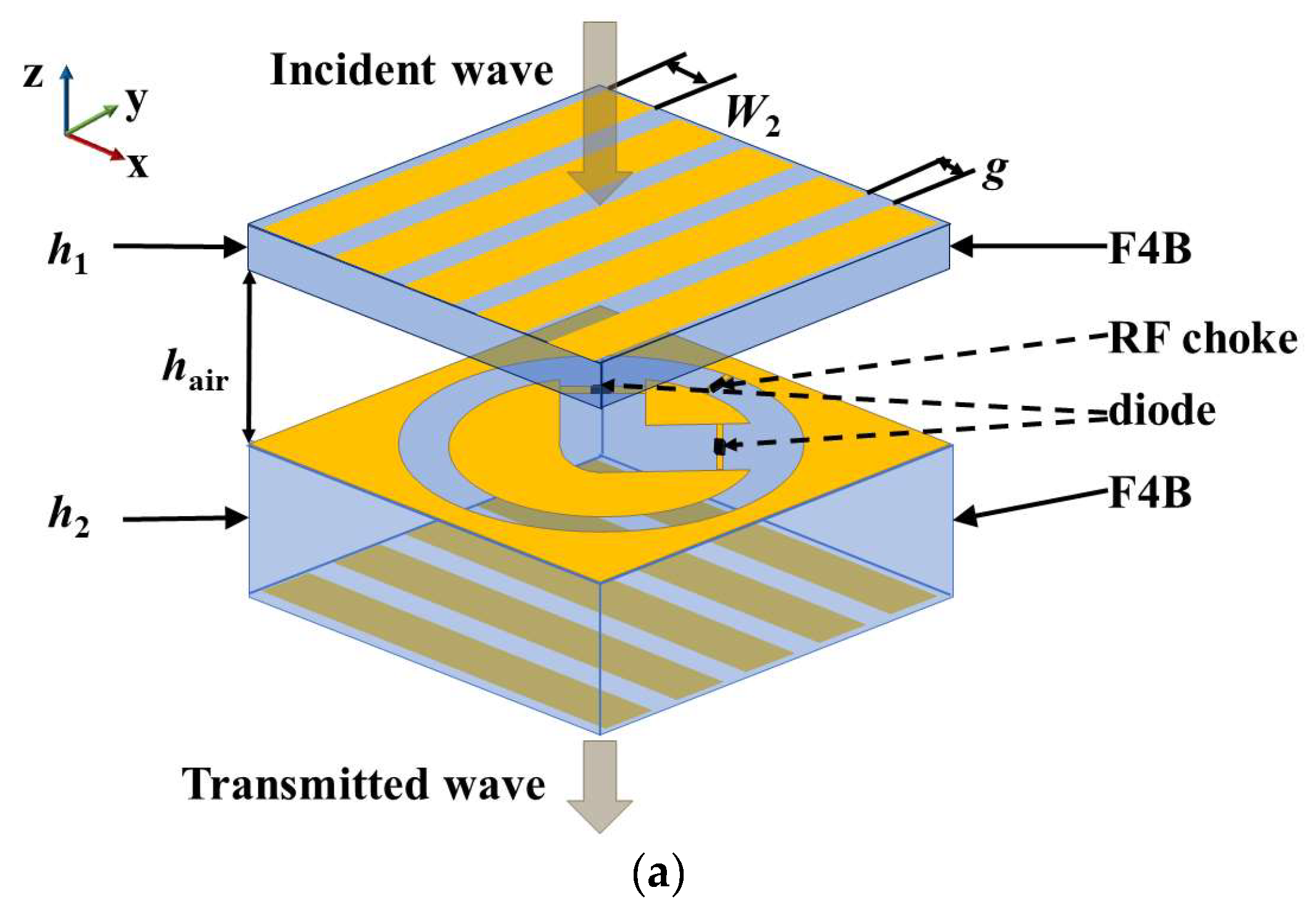
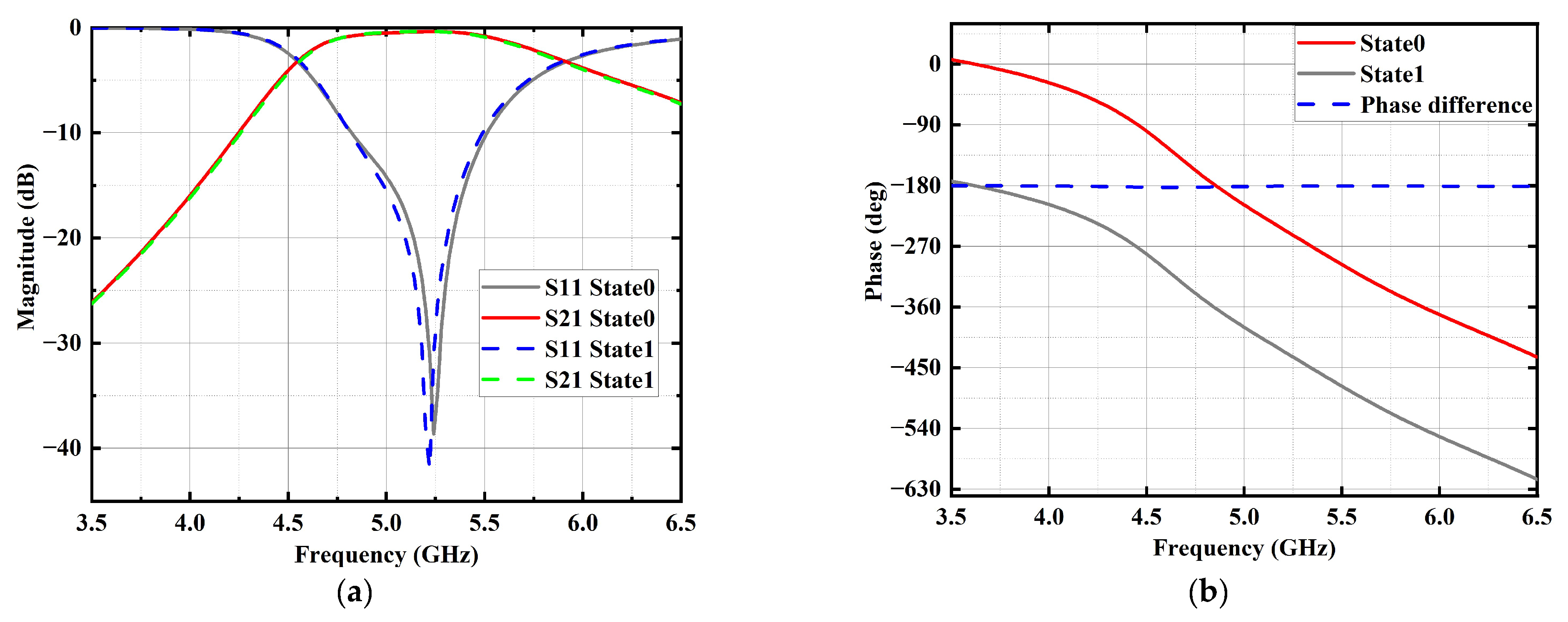
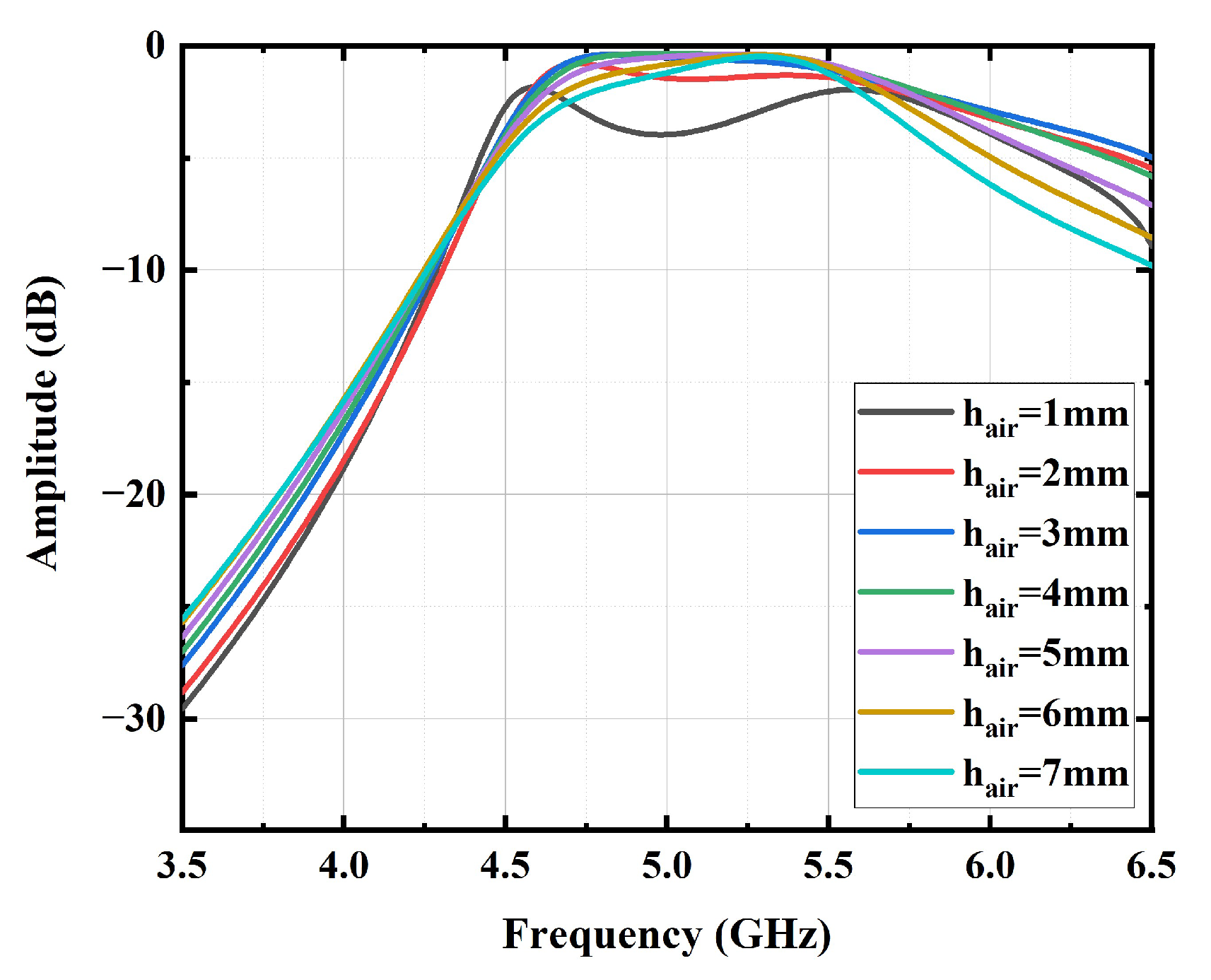
2.1. Unit Cell
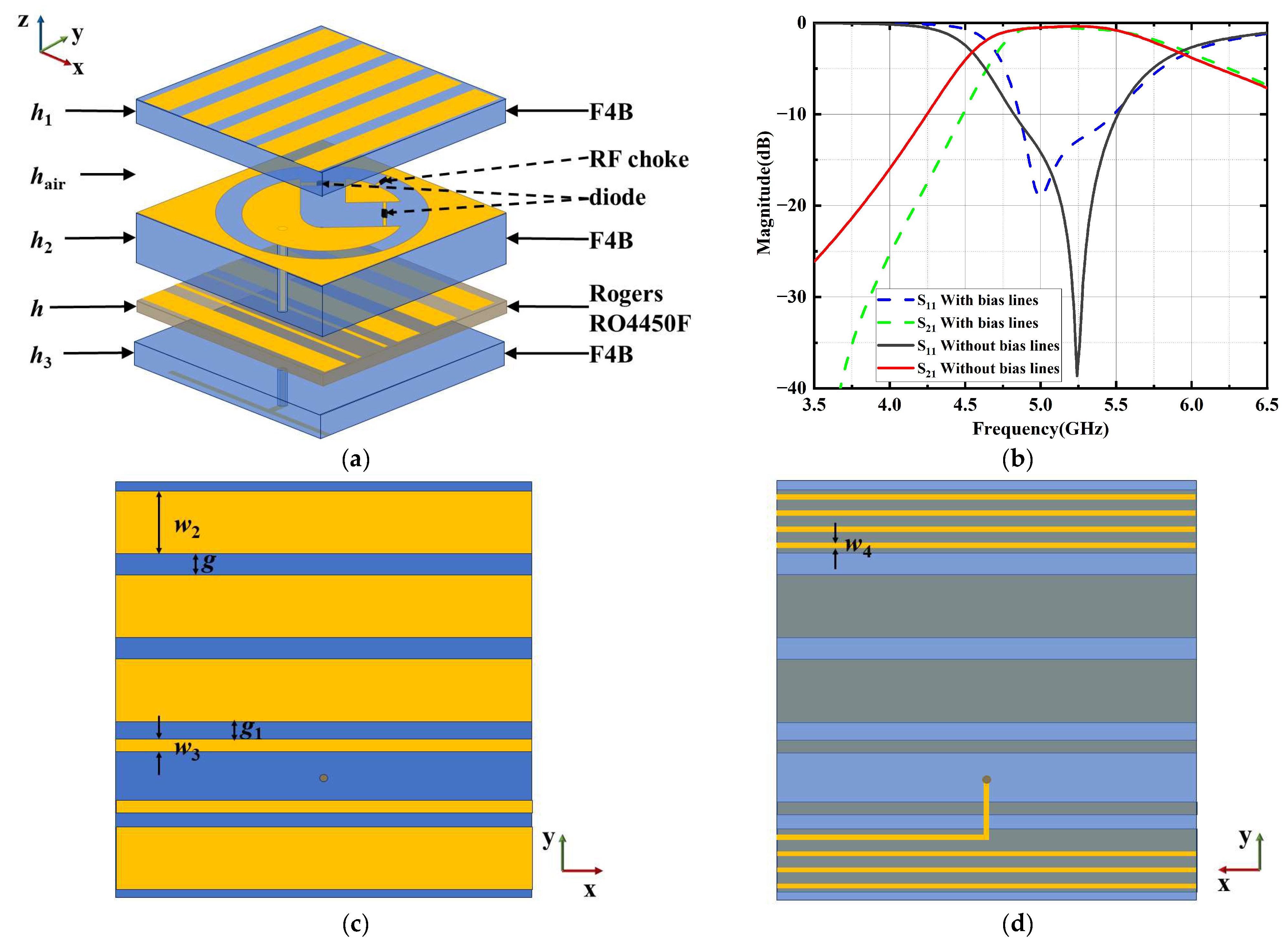
2.2. Bias Line
3. Transmitarray Design and Measurement
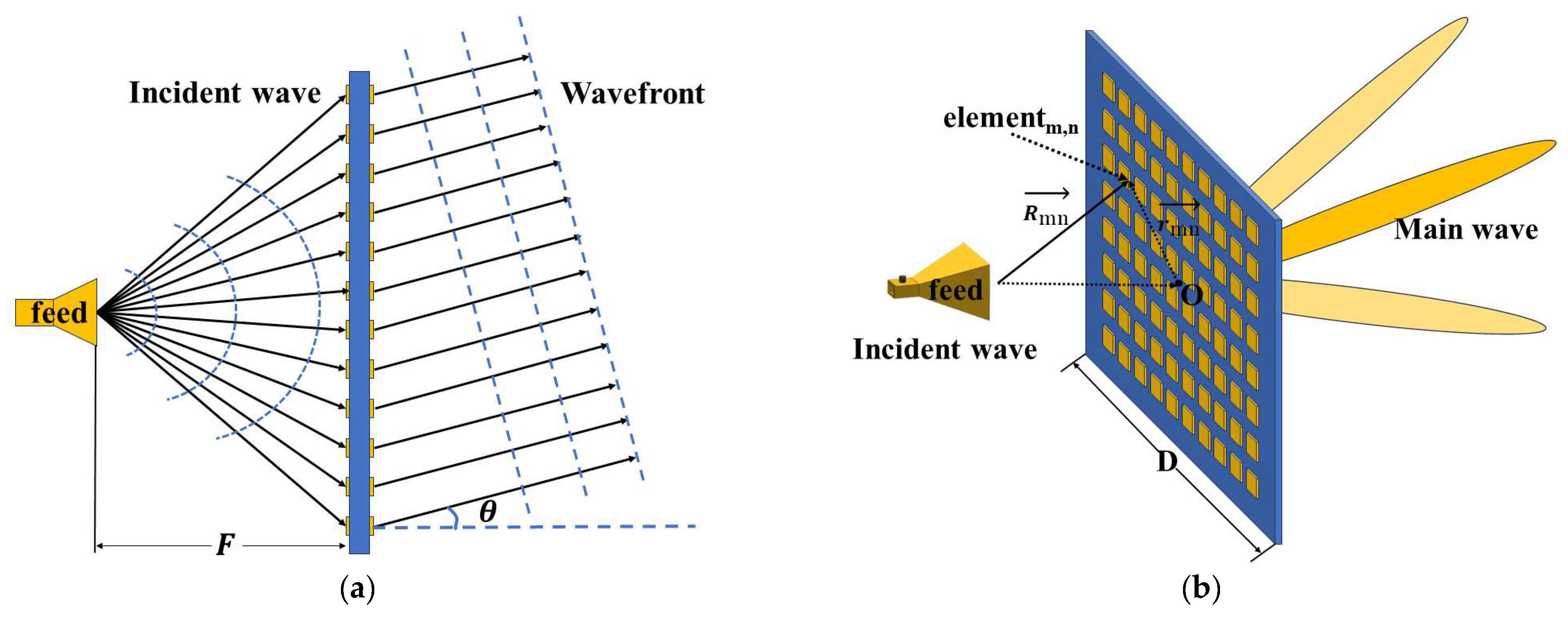
3.1. Transmitarray Beam Scanning Theory
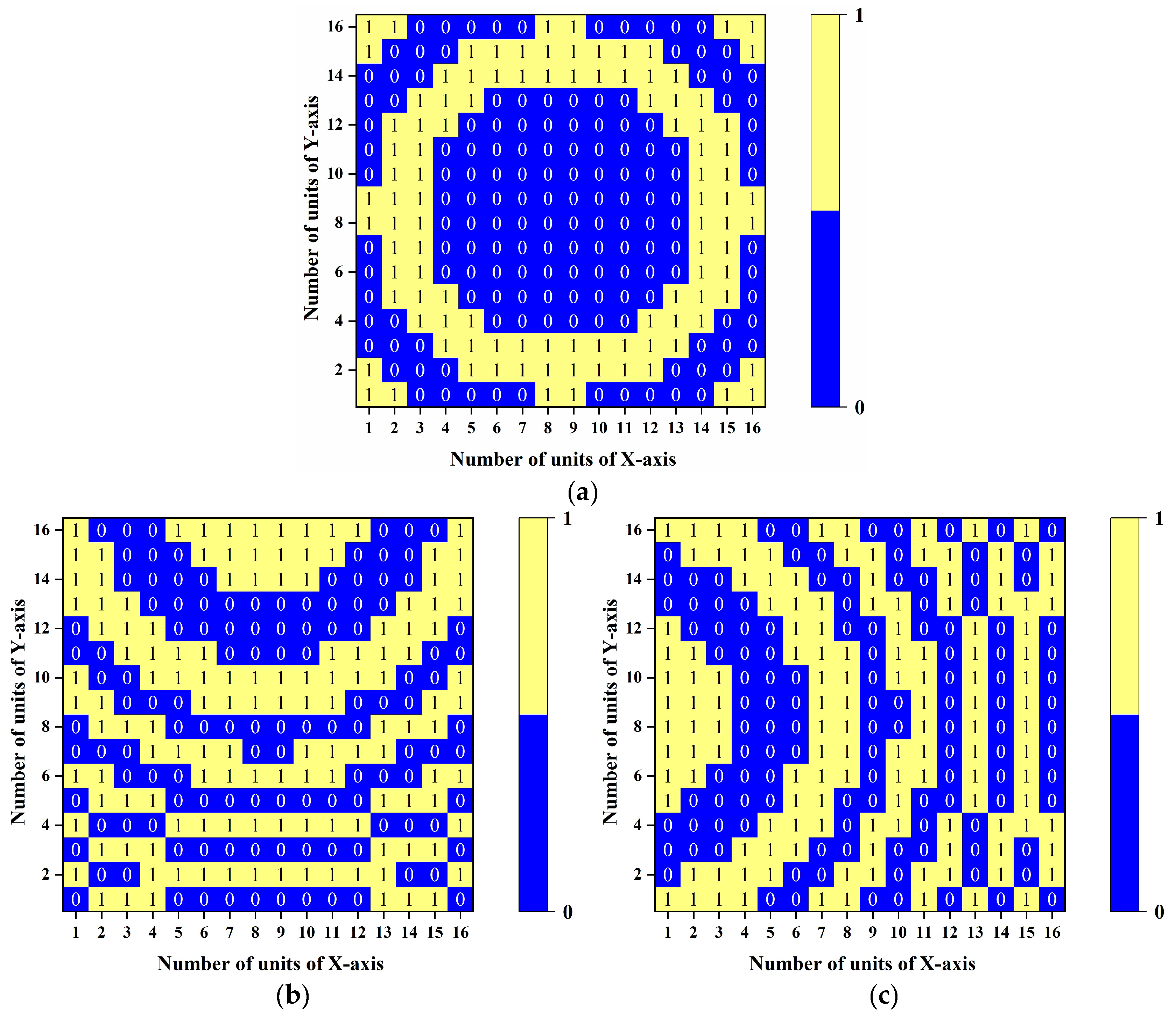
3.2. Transmitarray Design
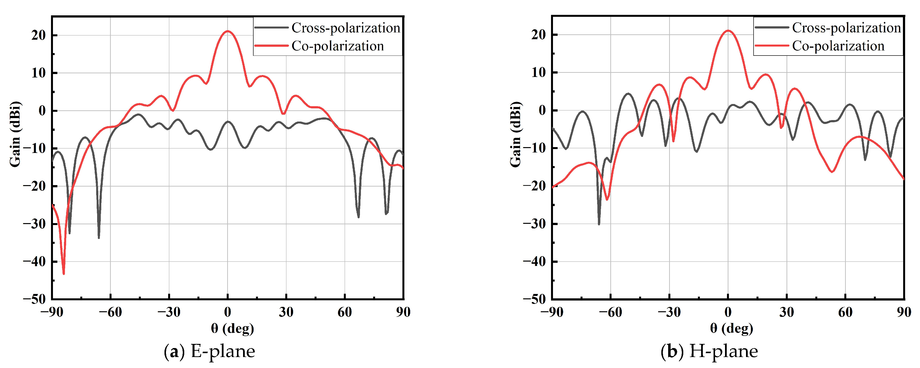
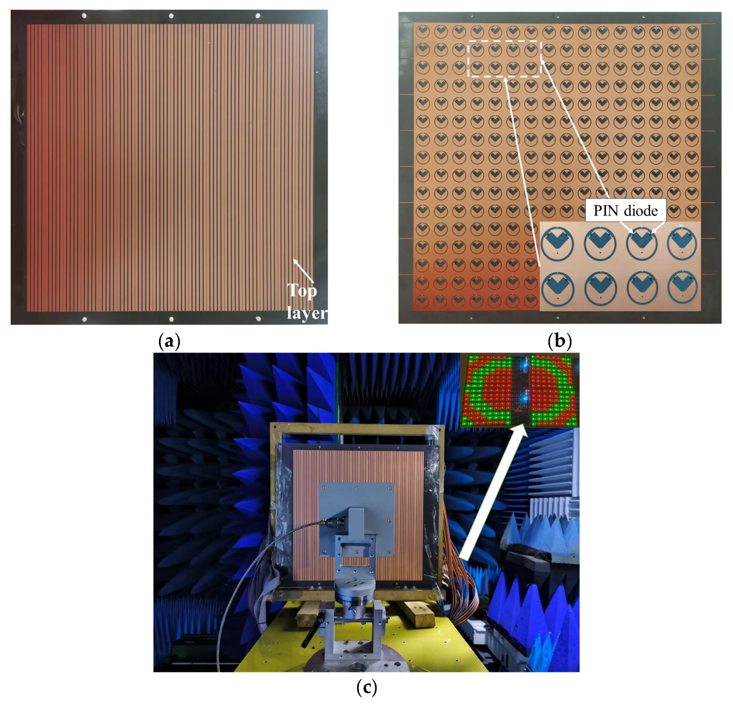
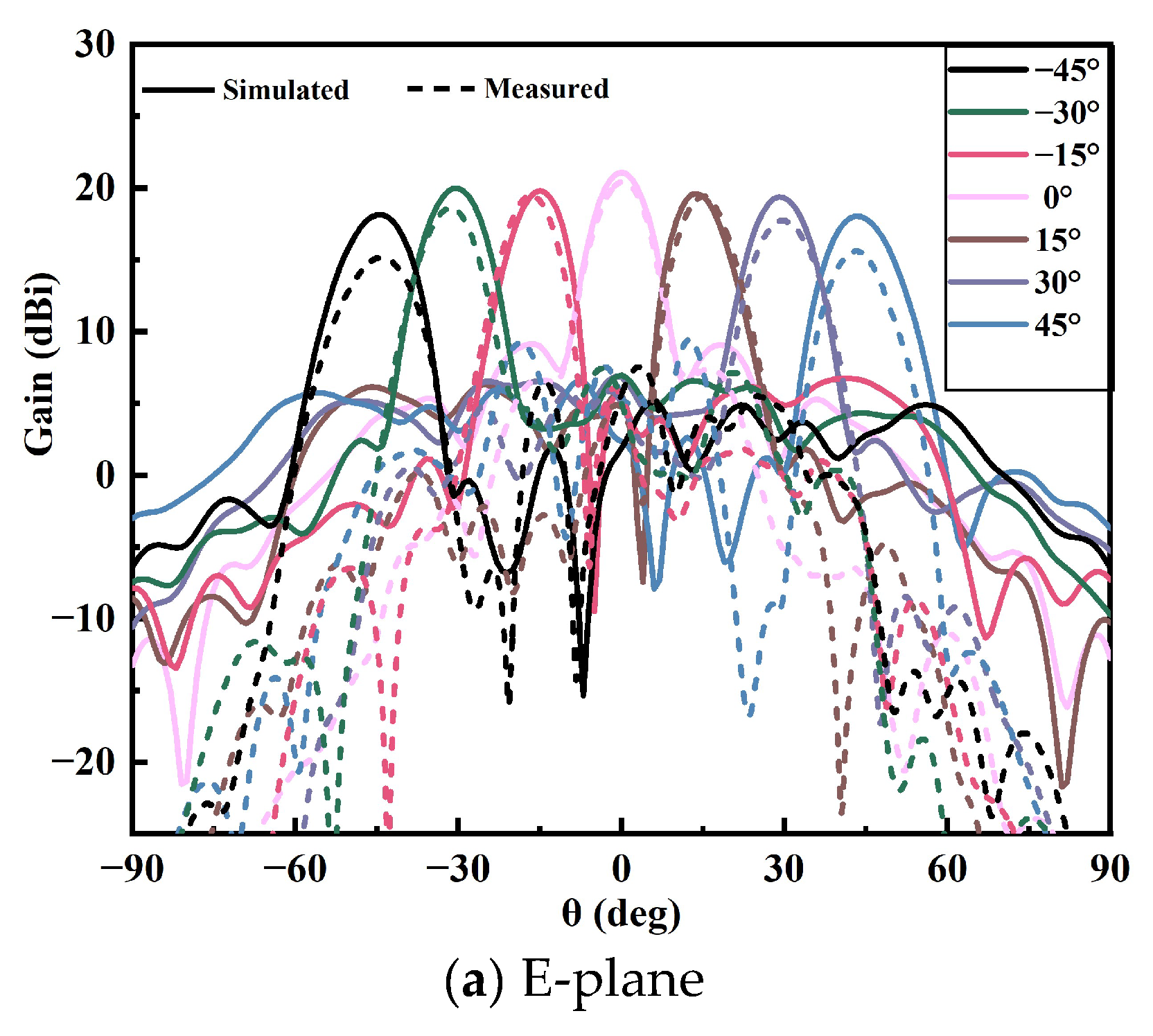
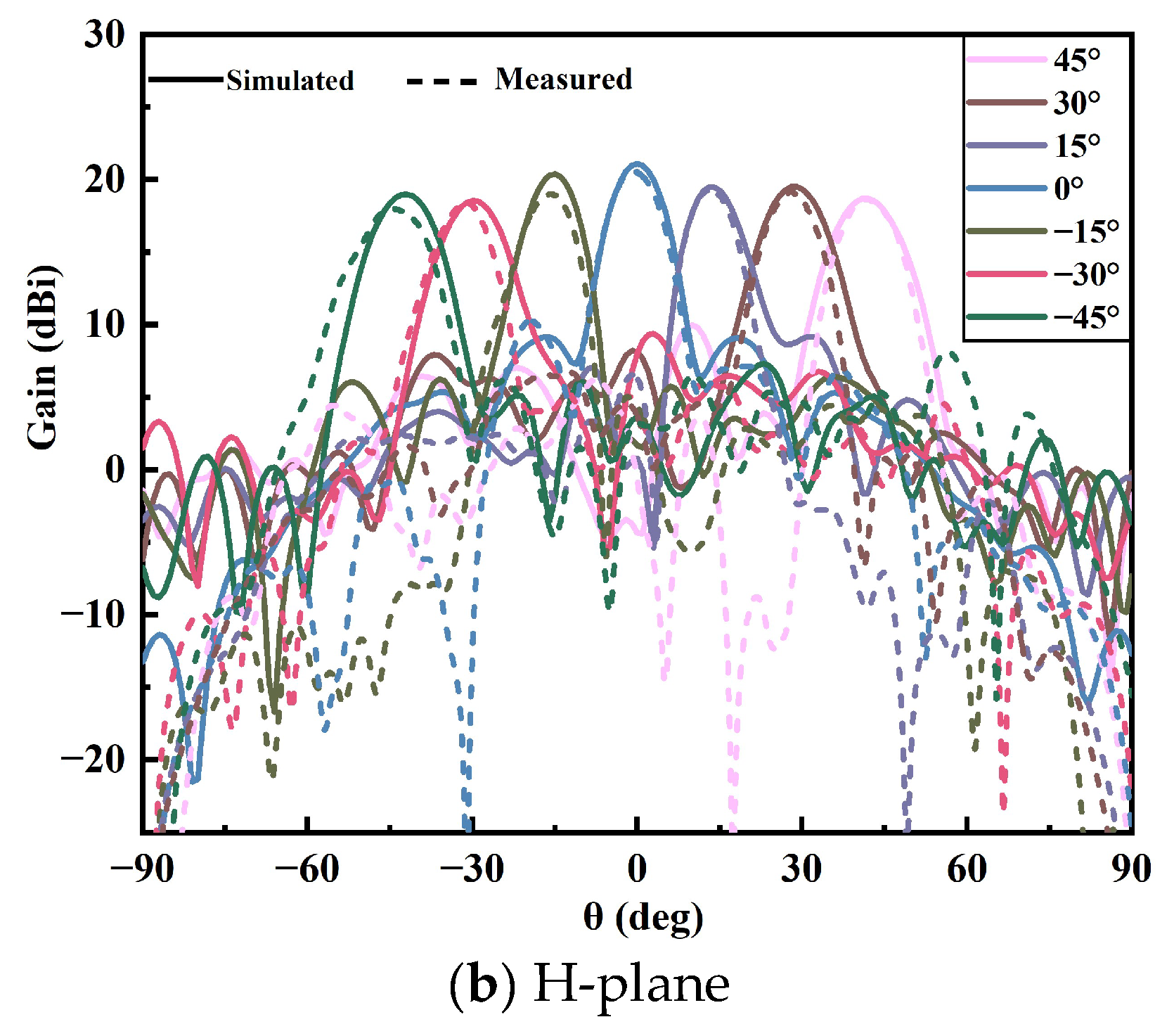
3.3. Measurement Results
4. Conclusions
Author Contributions
Funding
Data Availability Statement
Conflicts of Interest
References
- Yusuf, Y.; Gong, X. A Low-Cost Patch Antenna Phased Array With Analog Beam Steering Using Mutual Coupling and Reactive Loading. IEEE Antennas Wirel. Propag. Lett. 2008, 7, 81–84. [Google Scholar] [CrossRef]
- Raeesi, A.; Palizban, A.; Ehsandar, A.; Al-Saedi, H.; Gigoyan, S.; Abdel-Wahab, W.M.; Safavi-Naeini, S. A Low-Profile 2D Passive Phased-Array Antenna-in-Package for Emerging Millimeter-Wave Applications. IEEE Trans. Antennas Propag. 2023, 71, 1093–1098. [Google Scholar] [CrossRef]
- Nguyen, B.D.; Pichot, C. Unit-Cell Loaded With PIN Diodes for 1-Bit Linearly Polarized Reconfigurable Transmitarrays. IEEE Antennas Wirel. Propag. Lett. 2019, 18, 98–102. [Google Scholar] [CrossRef]
- Debogovic, T.; Perruisseau-Carrier, J. Low Loss MEMS-Reconfigurable 1-Bit Reflectarray Cell With Dual-Linear Polarization. IEEE Trans. Antennas Propag. 2014, 62, 5055–5060. [Google Scholar] [CrossRef]
- Baumgartner, M.; Ghasr, M.T.; Zoughi, R. Broadband dual varactor diode-loaded elliptical slot antenna with an orthogonal feed at K-band. In Proceedings of the 2013 IEEE International Instrumentation and Measurement Technology Conference (I2MTC), Minneapolis, MN, USA, 6–9 May 2013; pp. 635–640. [Google Scholar]
- Carrasco, E.; Barba, M.; Encinar, J.A. X-Band Reflectarray Antenna With Switching-Beam Using PIN Diodes and Gathered Elements. IEEE Trans. Antennas Propag. 2012, 60, 5700–5708. [Google Scholar] [CrossRef]
- Ning, Y.; Zhu, S.; Chu, H.; Zou, Q.; Zhang, C.; Li, J.; Xiao, P.; Li, G. 1-Bit Low-Cost Electronically Reconfigurable Reflectarray and Phased Array Based on PIN Diodes for Dynamic Beam Scanning. IEEE Trans. Antennas Propag. 2023, 72, 2007–2012. [Google Scholar] [CrossRef]
- Pereira, R.; Gillard, R.; Sauleau, R.; Potier, P.; Dousset, T.; Delestre, X. Dual Linearly-Polarized Unit-Cells With Nearly 2-Bit Resolution For Reflectarray Applications In X-Band. IEEE Trans. Antennas Propag. 2012, 60, 6042–6048. [Google Scholar] [CrossRef]
- Wu, F.; Zhao, W.G.; Xia, X.; Wang, J.; Jiang, Z.H.; Sauleau, R.; Hong, W. A 2 bit Circularly Polarized Reconfigurable Reflectarray Using p-i-n-Diode-Tuned Crossed-Bowtie Patch Elements. IEEE Trans. Antennas Propag. 2023, 71, 7299–7309. [Google Scholar] [CrossRef]
- Cuong, H.D.; Le, M.T.; Dinh, N.Q.; Tran, X.N.; Michishita, N. A Broadband 1-Bit Single-Layer Reconfigurable Reflectarray Unit Cell Based on PIN Diode Model. IEEE Access 2023, 11, 6477–6489. [Google Scholar] [CrossRef]
- Zhou, S.G.; Zhao, G.; Xu, H.; Luo, C.W.; Sun, J.Q.; Chen, G.T.; Jiao, Y.C. A Wideband 1-Bit Reconfigurable Reflectarray Antenna at Ku-Band. IEEE Antennas Wirel. Propag. Lett. 2022, 21, 566–570. [Google Scholar] [CrossRef]
- Clemente, A.; Dussopt, L.; Sauleau, R.; Potier, P.; Pouliguen, P. Wideband 400-Element Electronically Reconfigurable Transmitarray in X Band. IEEE Trans. Antennas Propag. 2013, 61, 5017–5027. [Google Scholar] [CrossRef]
- Le, D.D.; Nguyen, B.D.; Nguyen, M.T.; Tran, V.S. X-band transmitarray unit-cell with 1-bit phase control. In Proceedings of the 2017 IEEE Conference on Antenna Measurements & Applications (CAMA), Tsukuba, Japan, 4–6 December 2017; pp. 385–388. [Google Scholar]
- Nguyen, M.T.; Nguyen, B.D. 1-bit Unit-Cell For Ka-band Reconfigurable Transmitarrays. In Proceedings of the 2021 International Symposium on Antennas and Propagation (ISAP), Taipei, Taiwan, 19–22 October 2021; pp. 1–2. [Google Scholar]
- Wang, M.; Xu, S.; Yang, F.; Hu, N.; Xie, W.; Chen, Z. A Novel 1-Bit Reconfigurable Transmitarray Antenna Using a C-Shaped Probe-Fed Patch Element With Broadened Bandwidth and Enhanced Efficiency. IEEE Access 2020, 8, 120124–120133. [Google Scholar] [CrossRef]
- Wang, Y.; Xu, S.; Yang, F.; Li, M. A Novel 1 Bit Wide-Angle Beam Scanning Reconfigurable Transmitarray Antenna Using an Equivalent Magnetic Dipole Element. IEEE Trans. Antennas Propag. 2020, 68, 5691–5695. [Google Scholar] [CrossRef]
- Wang, Y.; Xu, S.; Yang, F.; Werner, D.H. 1 Bit Dual-Linear Polarized Reconfigurable Transmitarray Antenna Using Asymmetric Dipole Elements With Parasitic Bypass Dipoles. IEEE Trans. Antennas Propag. 2021, 69, 1188–1192. [Google Scholar] [CrossRef]
- Wang, M.; Xu, S.; Yang, F.; Li, M. Design and Measurement of a 1-bit Reconfigurable Transmitarray With Subwavelength H-Shaped Coupling Slot Elements. IEEE Trans. Antennas Propag. 2019, 67, 3500–3504. [Google Scholar] [CrossRef]
- Vilenskiy, A.R.; Makurin, M.N.; Lee, C.; Ivashina, M.V. Reconfigurable Transmitarray With Near-Field Coupling to Gap Waveguide Array Antenna for Efficient 2-D Beam Steering. IEEE Trans. Antennas Propag. 2020, 68, 7854–7865. [Google Scholar] [CrossRef]
- Grady, N.K.; Heyes, J.E.; Chowdhury, D.R.; Zeng, Y.; Reiten, M.T.; Azad, A.K.; Taylor, A.J.; Dalvit, D.A.R.; Chen, H.T. Broadband and high-efficiency terahertz metamaterial linear polarization converters. In Proceedings of the 2013 38th International Conference on Infrared, Millimeter, and Terahertz Waves (IRMMW-THz), Mainz, Germany, 1–6 September 2013; pp. 1–3. [Google Scholar]
- Yin, L.; Xue, Z.; Ren, W.; Lv, Q.; Zhang, B.; Jin, C. High-Roll-Off-Rate Ultrathin Polarization-Rotating Frequency Selective Surface. IEEE Antennas Wirel. Propag. Lett. 2023, 22, 1592–1596. [Google Scholar] [CrossRef]
- Yin, L.; Jin, C.; Lv, Q.; Zhang, B.; Cao, K.; Zhang, P.; Xue, Z. Amplitude and Phase Independently Adjustable Transmitarray Aperture and Its Applications to High Gain and Low Sidelobe Antenna. IEEE Trans. Antennas Propag. 2022, 70, 4498–4506. [Google Scholar] [CrossRef]
- Yu, H.; Su, J.; Li, Z.; Yang, F. A Novel Wideband and High-Efficiency Electronically Scanning Transmitarray Using Transmission Metasurface Polarizer. IEEE Trans. Antennas Propag. 2022, 70, 3088–3093. [Google Scholar] [CrossRef]
- Abdelrahman, A.H.; Elsherbeni, A.Z.; Yang, F. Transmission Phase Limit of Multilayer Frequency-Selective Surfaces for Transmitarray Designs. IEEE Trans. Antennas Propag. 2014, 62, 690–697. [Google Scholar] [CrossRef]
- Abdelrahman, A.H.; Yang, F.; Elsherbeni, A.Z. Analysis and Design of Transmitarray Antennas; Morgan & Claypool Publishers: New York, NY, USA, 2017. [Google Scholar]
- Diaby, F.; Clemente, A.; Sauleau, R.; Pham, K.T.; Dussopt, L. 2 Bit Reconfigurable Unit-Cell and Electronically Steerable Transmitarray at $Ka$ -Band. IEEE Trans. Antennas Propag. 2020, 68, 5003–5008. [Google Scholar] [CrossRef]


| Ref. No. | Freq. (GHz) | Array Size () | Max Gain (dBi) | Max Aperture Efficiency | Scanning Range and Loss | Profile Height () |
|---|---|---|---|---|---|---|
| [12] [3] | 9.8 11.5 | 9.8 9.8 6.44 6.44 | 22.7 21.0 | 15.4% 24.1% | (1.9 dB) (3 dB) | 0.102 0.19 |
| [18] | 12.5 | 5.3 5.3 | 17.0 | 14.0% | (5.8 dB) | 0.0875 |
| [19] | 25 | 0.65 0.65 | 17.5 | 20% | (3 dB) | 1.7 |
| [26] | 10.5 | 0.28 0.28 | 19.8 | 15.9% | (5 dB) | 0.125 |
| [16] This work | 13.5 5.0 | 8.6 8.6 6.67 6.67 | 21.4 20.59 | 15.4% 20.5% | (3.6 dB) (2.96 dB) | 0.07 0.17 |
Disclaimer/Publisher’s Note: The statements, opinions and data contained in all publications are solely those of the individual author(s) and contributor(s) and not of MDPI and/or the editor(s). MDPI and/or the editor(s) disclaim responsibility for any injury to people or property resulting from any ideas, methods, instructions or products referred to in the content. |
© 2024 by the authors. Licensee MDPI, Basel, Switzerland. This article is an open access article distributed under the terms and conditions of the Creative Commons Attribution (CC BY) license (https://creativecommons.org/licenses/by/4.0/).
Share and Cite
Zheng, Z.; Ren, W.; Li, W.; Xue, Z. A New 1 Bit Electronically Reconfigurable Transmitarray. Electronics 2024, 13, 1383. https://doi.org/10.3390/electronics13071383
Zheng Z, Ren W, Li W, Xue Z. A New 1 Bit Electronically Reconfigurable Transmitarray. Electronics. 2024; 13(7):1383. https://doi.org/10.3390/electronics13071383
Chicago/Turabian StyleZheng, Zizhen, Wu Ren, Weiming Li, and Zhenghui Xue. 2024. "A New 1 Bit Electronically Reconfigurable Transmitarray" Electronics 13, no. 7: 1383. https://doi.org/10.3390/electronics13071383