Article

A 16 Bit 125 MS/s Pipelined Analog-to-Digital Converter with a Digital Foreground Calibration Based on Capacitor Reuse

1
State Key Laboratory of Materials for Integrated Circuits, Shanghai Institute of Microsystem and Information Technology, Chinese Academy of Sciences, Shanghai 200050, China
2
University of Chinese Academy of Sciences, Beijing 100049, China
3
Center of Materials Science and Optoelectronics Engineering, University of Chinese Academy of Sciences, Beijing 100049, China
*
Author to whom correspondence should be addressed.
These authors contributed equally to this work.
Electronics 2024, 13(8), 1474; https://doi.org/10.3390/electronics13081474
Submission received: 11 March 2024 / Revised: 9 April 2024 / Accepted: 11 April 2024 / Published: 12 April 2024
(This article belongs to the Section Circuit and Signal Processing)

Abstract

:
A 16-bit 125 MS/s pipelined analog-to-digital converter (ADC) implemented in a 0.18 μ m CMOS process is presented in this paper. A sample-and-hold amplifier-less (SHA-less) modified 2.5-bit front-end is adopted, which splits the sampling capacitor in half to eliminate the common-mode voltage buffer. The multiplying-digital-to-analog converter (MDAC) in the first pipeline stage is modified by reusing the sampling capacitor in a foreground digital calibration for improving the ADC linearity. This design can circumvent a dedicated reference buffer to generate the calibration voltages at all comparator thresholds. By calibrating the ADC in the digital domain, the integral non-linearity (INL) is improved from −9.2/10 LSB to −3/2.2 LSB, and the spurious-free dynamic range (SFDR) is optimized by over 8dB. The ADC consumes 154mW (reference buffer and clock included) from a 1.8 V supply.

1. Introduction

The boom of the wireless communication is driving the world into a ubiquitous information exchange environment, which strongly calls for high speed and high resolution analog-to-digital converters (ADCs). Pipelined ADC architectures outperform others for their better trade-off between speed and resolution [1]. However, as a CMOS device enters the nanoscale region, a mismatch between the capacitors in DACs (digital-to-analog converters) could severely degrade the linearity of a pipelined ADC. To tackle the problems mentioned above, some papers have reported approaches in the analog domain, which has suffered a lot from low power budgets and area overheads [2,3,4]. In [5,6,7,8], an additional calibration RDAC was introduced to extract the capacitor mismatch error of ADCs, store the error information in the RAM, and then quantize compensation. The extra analog circuits consume a lot of on-chip resources and a large area. In addition, the analog calibration is strictly limited by the ADC architecture because of its poor compatibility [9]. As a result, calibration techniques that detect and compensate for errors in the analog domain have been gradually replaced over time.
Recently, numerous researchers have investigated digital calibration techniques [10,11,12,13,14,15,16,17], since the scaling of CMOS device dimensions offers clear advantages for digital circuitry in terms of area, speed, and integration. According to whether the ADC is calibrated in real time, digital calibration technology is divided into foreground calibration and background calibration. Background calibration refers to when the ADC is calibrated while working, but it takes a period of time to converge. The algorithms reported in [18,19] have quite a fast convergence speed; however, they are ineffective at certain frequencies and can even deteriorate the ADC performance due to its own defects, whereas the digital background calibration algorithms in [20,21,22,23,24,25] do require the external input injection, such as a pseudo-random (PN) noise sequence [20,21,22,23] and sinusoidal signals [24] for calibration, which typically have convergence speeds in the order of approximately 10 6 to 10 8 cycles [20,21,22,23], 10 5 cycles, and 10 4 cycles [25]. Compared with the background calibration, the foreground one is much more reliable. Once powered on, the ADC is calibrated first. After calibration, the error code is usually stored in a one-time-programmable (OTP) or electronic fuse (Efuse) module. Furthermore, it is important to note that a calibrated ADC avoids the convergence time while working, so the ideal output can be obtained quickly.
This paper describes a digital foreground calibration technique based on the capacitor reuse to estimate the mismatch between capacitors in MDAC. The first two stages employ a modified MDAC, whose sampling capacitors are separated from the sub-DAC. In the calibration mode, one of the sampling capacitors is utilized to generate an equivalent calibration voltage of ± 1 8 V r e f and estimate the error code caused by capacitor mismatch. Reusing the capacitor in MDAC can eliminate the requirement for a dedicated reference buffer to generate the calibration voltage at all threshold voltages, thereby minimizing the chip size and significantly reducing the power consumption. Furthermore, the separated MDAC not only realizes the calibration target, but also eliminates the kickback effect on the input signal and reference buffer. In addition, we split the sampling capacitor in half to avoid the use of a common-mode voltage buffer. In this way, the power and area requirement can be relaxed further.
The paper is organized as follows: Section 2 describes the effect of a mismatched ADC output performance of the capacitor array in an MDAC. Section 3 introduces the pipeline ADC proposed by SHA-less type, including the structural principle of the improved MDAC capacitor array, the performance analysis, and the calibration algorithm principle based on the improved MDAC. Section 4 shows the results of the calibration algorithm based on a 180 nm process verification, and Section 5 provides the conclusion.

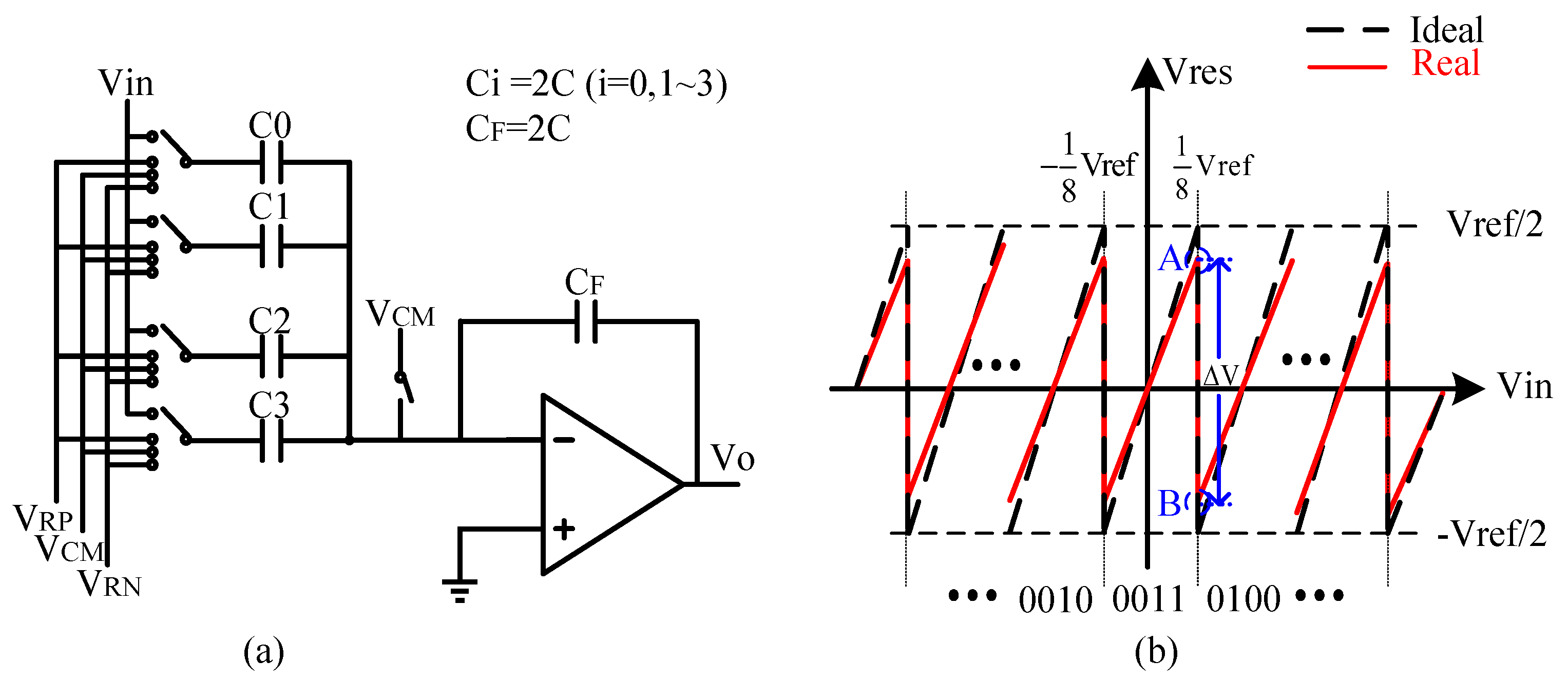
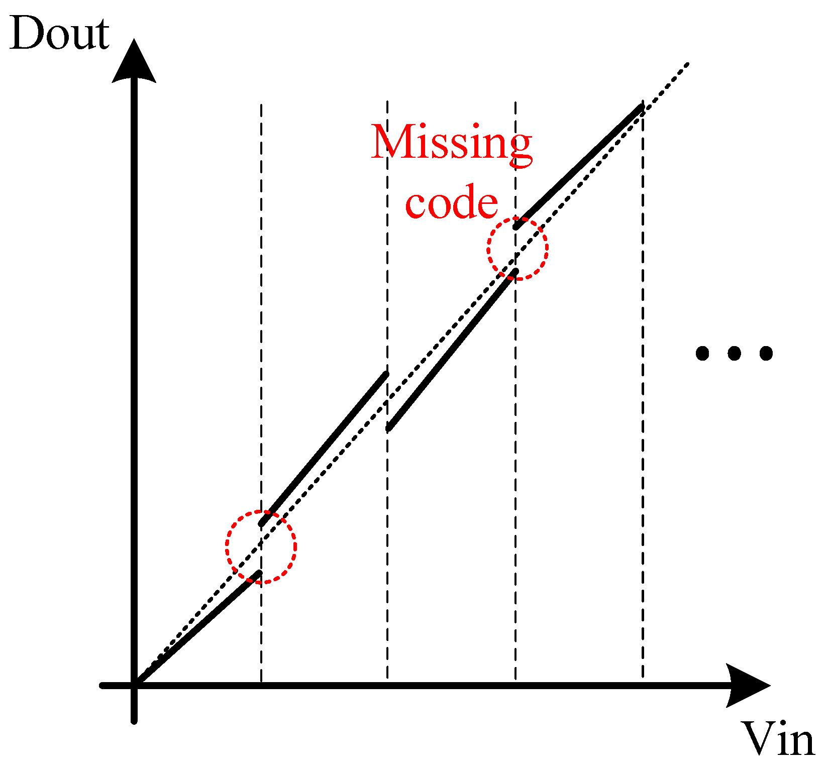
2. Capacitor Mismatch in MDAC

A traditional 2.5-bit MDAC is depicted in Figure 1a. For simplicity, only half of the differential implementation is shown. Ideally, all of the capacitors are equal to 2C under perfect matching. C is the unit capacitor of the MDAC, and the interstage gain is 4. The amplifier output can be expressed as follows:
V o = V i n × C T C F V r e f × ( C V R P C V R N ) C F
where C T is the total capacitance of the sampling capacitor, C i is the ith capacitor of the MDAC, C F is the feedback capacitor, and V r e f is the reference voltage of the ADC which is equal to V R P V R N . In Equation (1), the term with the footnote V R P ( V R N ) means the capacitor connecting to V R P ( V R N ).
Nevertheless, after the tape-out process, the capacitors in MDAC differ from each other due to the mismatch. Assuming that Δ C i is the deviation from an ideal capacitor C i , then Equation (1) can be rewritten as follows [2]:
V o = V i n × 4 + Δ C i C F V r e f × C + Δ C i V R P C F + V r e f × C + Δ C i V R N C F
where 4 is the interstage gain of the 2.5-bit MDAC.
Figure 1b shows the transfer curve. The deviation (black dotted line) from the ideal case (red solid line) can be seen from the plot in Figure 1b. Then, the residue voltage in Equation (2) is processed by the back-end pipelined stages. To observe the mismatch effect on the ADC output code, the same V i n is quantized by the adjacent residue transfer curve in the neighbored subranges. The shifting voltage Δ V and the error voltage V e r r at comparator thresholds can be expressed as follows:
Δ V = 1 + Δ C i C F × V r e f ,
V e r r = Δ C i C F × V r e f .
The output results of the ADC are depicted in Figure 2. Obviously, there are many “jumps” at each of the two adjacent subranges. Attention should be paid when V e r r < 0 because the missing code decreases the ADC performance greatly [26]. Thus, if the V e r r can be measured and compensated for in a certain way, we can eliminate the nonlinearity caused by capacitor mismatch.

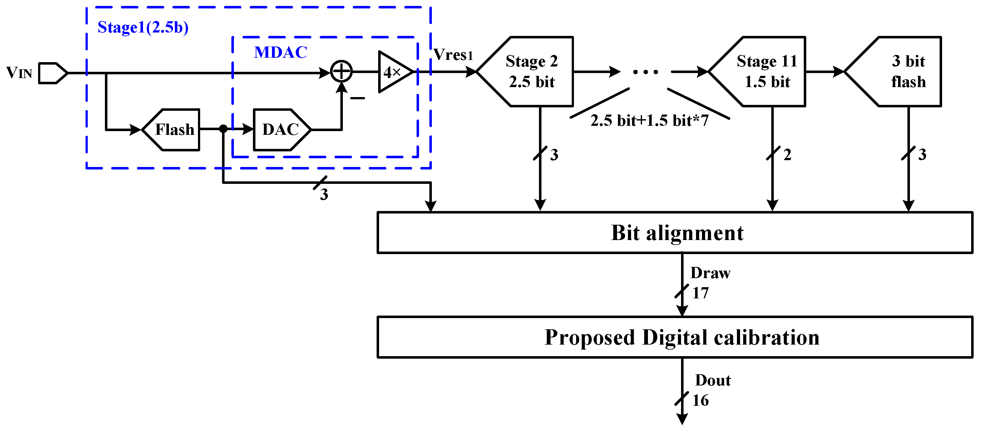
3. Proposed 16 Bit SHA-Less Pipelined ADC

The implementation of the proposed pipelined ADC is shown in Figure 3. The pipelined ADC is SHA-less, where the sample-and-hold circuit is integrated with the first-stage MDAC. Taking the power and noise into consideration, the first three stages resolve 2.5 bits, which is then followed by eight stages with 1.5-bit/stage and a 3-bit back-end flash ADC. After that, all the stage output bits are sent to the digital bit alignment block. Furthermore, the capacitor mismatches in first and second stages need to be calibrated for a desired linearity.
As the diagram shows, all the 17 bits codes obtained from each stage are fed to the digital module to reconstruct the digital output. Here, an extra bit obtained from the pipelined stages is used for decreasing the quantization noise. After that, for a higher linearity, the proposed digital foreground calibration is employed.

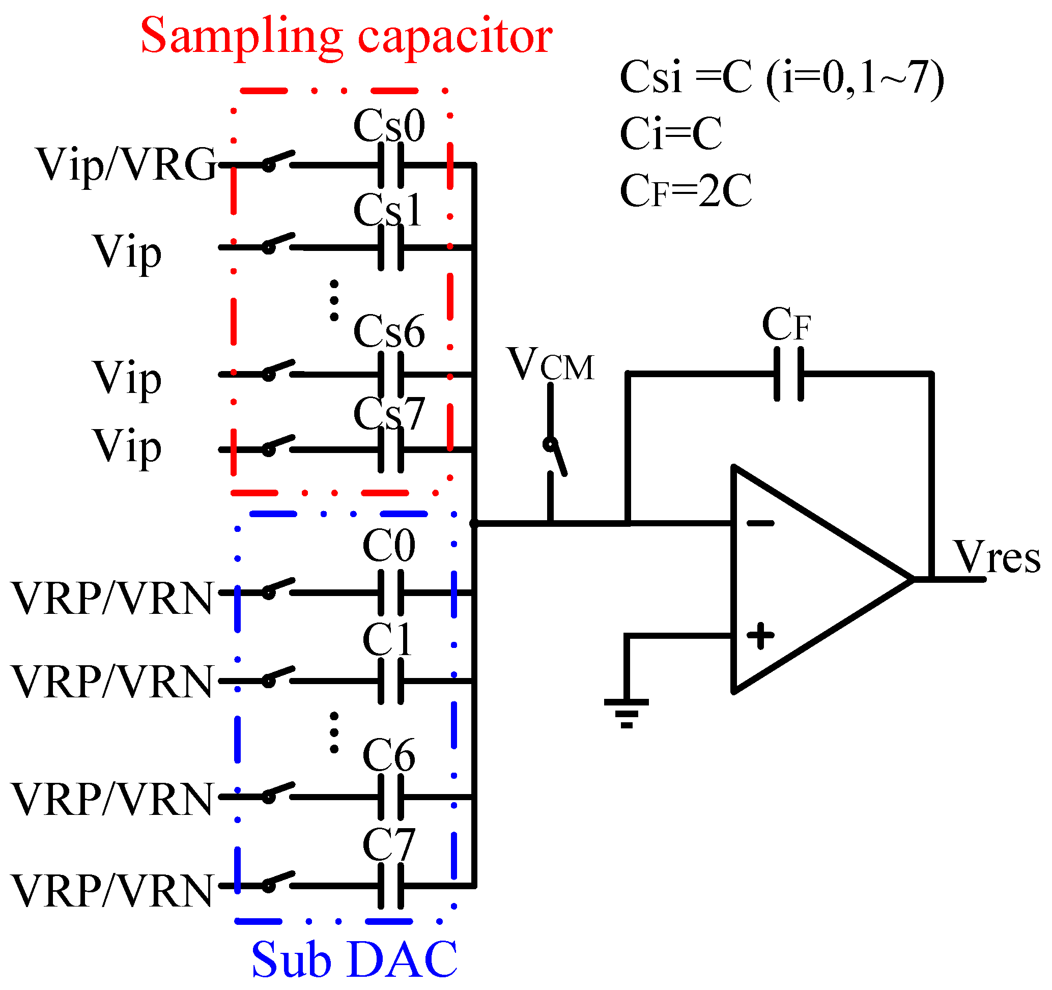
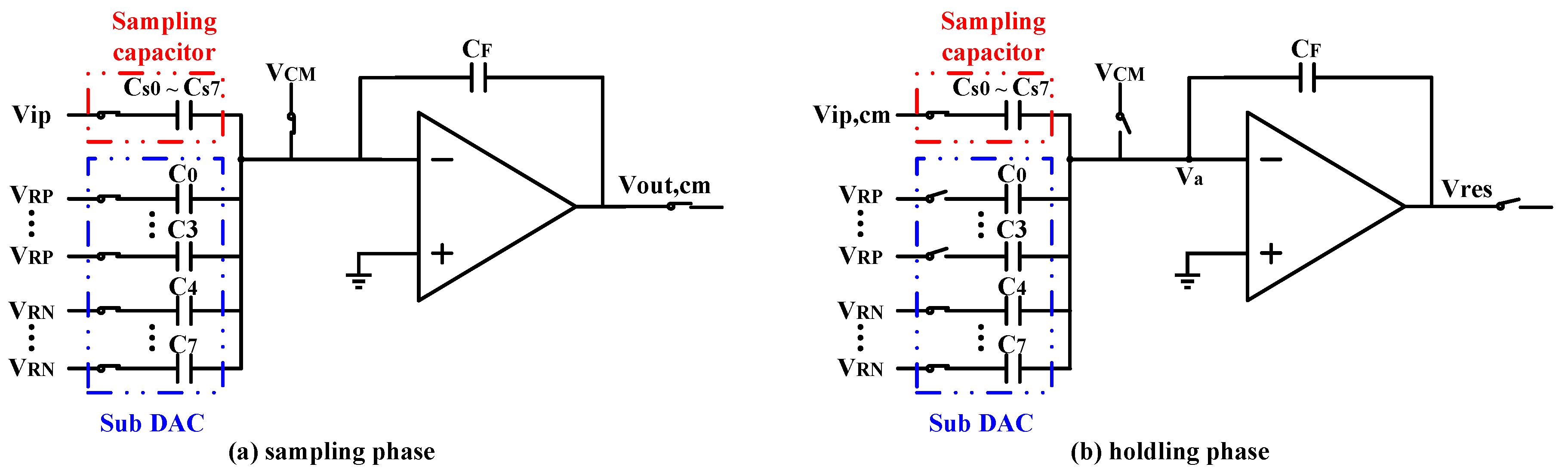
3.1. Modified MDAC in the First Stage

The 2.5-bit MDAC we propose is shown in Figure 4. Compared with the traditional one in Figure 1a, we separate the sampling capacitors C s i (i = 0, 1…7) from the sub-DAC capacitors.
This study adopted the bottom plate sampling technique. Under a normal conversion mode, in the sampling phase, for example, φ 1, the differential input voltage is sampled to the bottom plates of the MDAC. For simplicity, only the single-ended structure is display here. As shown here in Figure 5a, all the top plate of the capacitors in MDAC are applied to a common-mode voltage V C M , whereas for the bottom plate, the situation is different. The input voltage Vip is supplied to the sampling capacitors C s i (i = 0, 1,…7), while the V R P and V R N are connected to C i (i = 0∼3) and C i (i = 4∼7) in sub-DAC, respectively. At the same time, the output of the opamp is switched to the output common-mode voltage V o u t , c m .
By switching the capacitor array in phase φ 1, the differential charge sampled on the capacitors can be expressed as Equation (5):
Q 1 = ( V i p V i n ) × i = 0 7 C s i ,
where V I N = V i p V i n , V r e f = V R P V R N . In the holding phase φ 2 shown in Figure 5b, the top plate is open from V C M . The input voltage is changed to a stable-input common-mode voltage V I N , c m . For the capacitors in a sub-DAC, C i (i = 0∼7) are switched to V R N or V R P according to the comparator results D ( i ) . When D ( i ) = 1, C i is switched to V R N ; otherwise, C i is switched to V R P . Therefore, the charge in holding phase φ 2 can be expressed as Equation (6):
Q 2 = ( V R P V R N ) × i = 0 7 C i [ 1 2 D ( i ) ] V r e s × C F = V r e f × i = 0 7 C i [ 1 2 D ( i ) ] V r e s × C F .
C F is the feedback capacitor of the MDAC, which is equal to 2C. As the result of charge conservation, Q 1 equals Q 2 . Finally, the transfer function of the modified MDAC can be obtained:
V r e s = C T C F V I N i = 0 7 2 D ( i ) 1 × C i C T × V r e f ,
where C T refers to the total capacitance of sampling capacitor; C i = C + Δ C i .
The use of separated sampling capacitors offers many advantages over the reuse of a sub-DAC to process the sampling and quantization. Firstly, there is no charge redistribution on C s in the holding phase, which, avoiding the reset pulse before C s , goes back to track. Secondly, the kickback effect of a charge glitch on a reference buffer is decreased [27]. Furthermore, the structure for splitting the unit capacitor in half is free from the common-mode voltage buffer compared with the conventional one.
Based on the modified MDAC, reusing 1/8 of the sampling capacitors (e.g., C s 0 ) as the assistant capacitor in the calibration mode can also generate a calibration voltage ( ± 1 8 V r e f ) without an extra circuit implementation. Cooperating with the switching scheme mentioned later, all the capacitor mismatches in a sub-DAC can be calibrated in the absence of the dedicated reference buffer, which relaxes the area and power overhead greatly.

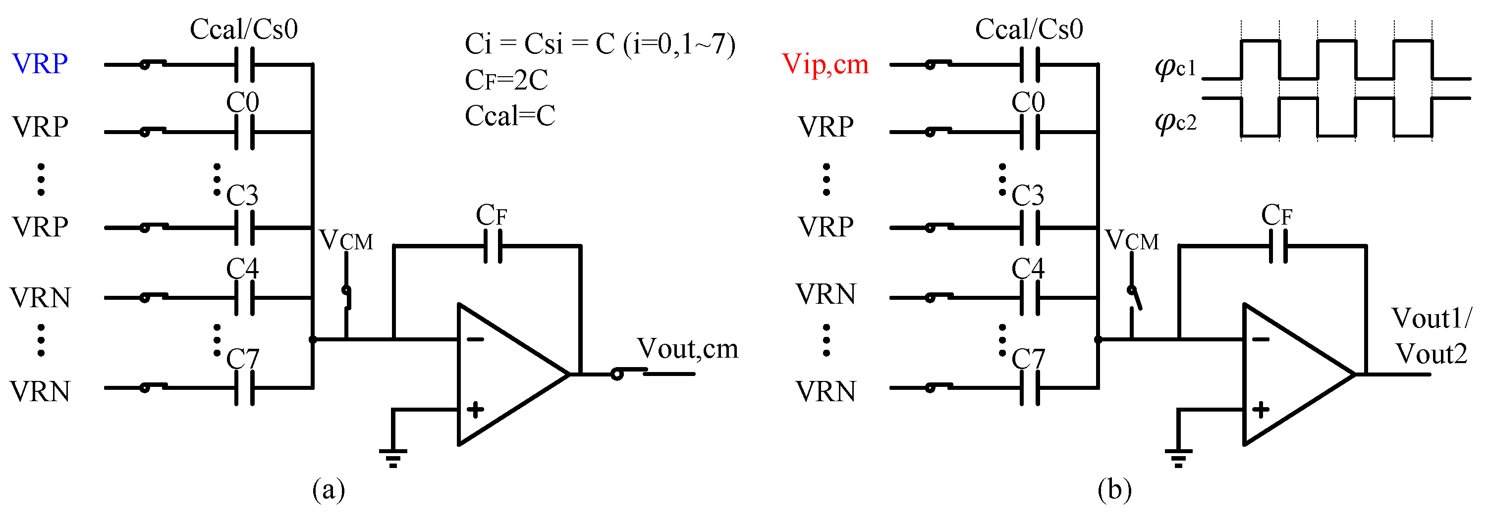
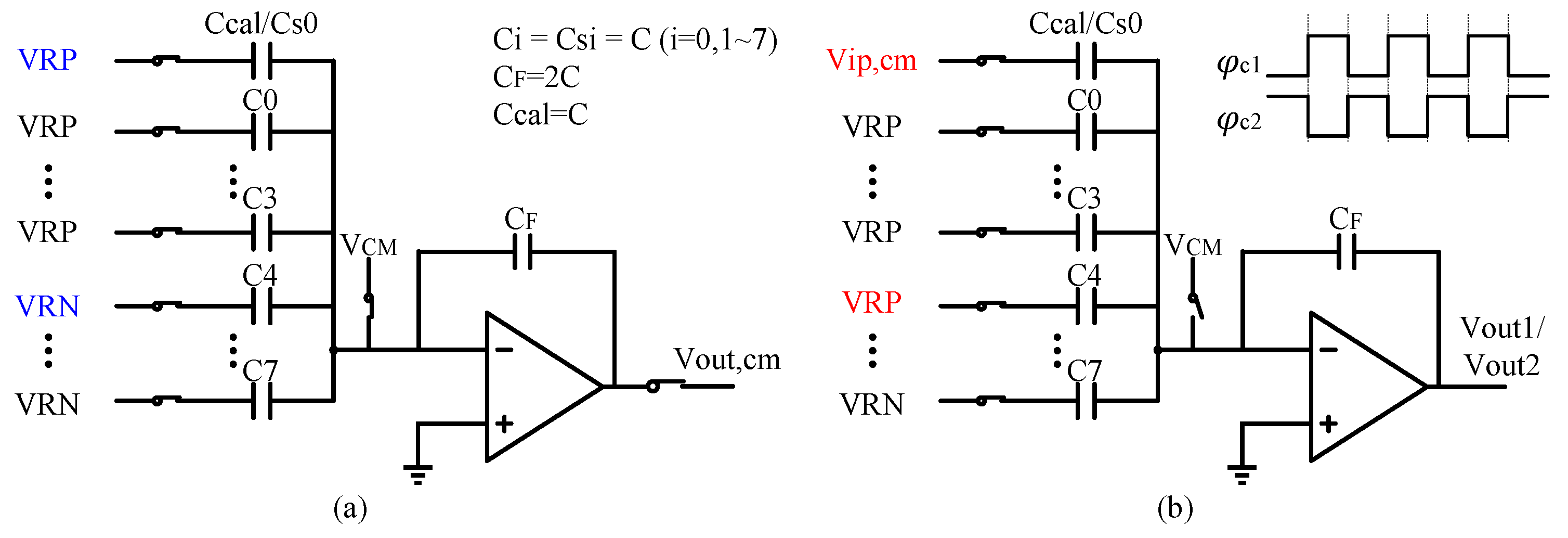
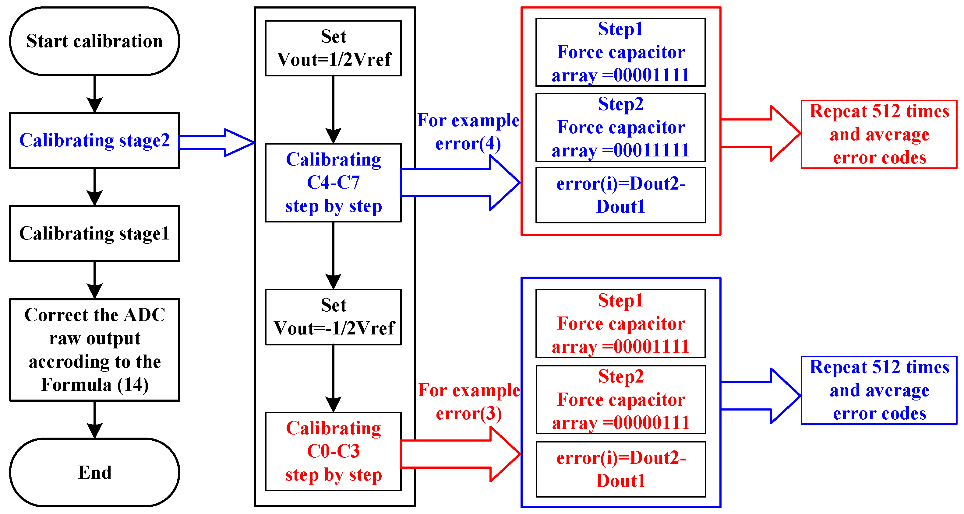
3.2. Calibration Technique

In practice, owing to the interstage gain of the pipelined ADC, the mismatches of the back-end stages can be neglected. Here, we choose the first two stages for calibration. Once the ADC is powered on, the calibration process starts. The first two stages’ amplifiers are shown in Figure 6 for a single-ended implementation. Without any hardware costs, C s 0 in MDAC1 is reused directly to generate the threshold voltages in the first stage of calibration. A capacitor C c a l is regarded as the unique assistant capacitor when calibrating in stage2.
As shown in Figure 6, when calibrating stage1, the capacitors C i (i = 0, 1…7) are switched to “00001111” in sampling phase φ c1, meaning that the capacitors C 0 C 3 are switched to V R P and the capacitors C 4 C 7 are switched to V R N . It is equivalent to connecting the input of stage1 to GND. After that, V R P is applied to the reused capacitor C s 0 , where C s 0 = C. All the top plate are connected to V C M . Quantitatively, the charge Q c 1 sampled differentially in phase φ c1 can be represented as follows:
Q c 1 = V R P V R N × C S 0 + V R P V R N × i = 0 3 C i V R P V R N × i = 4 7 C i .
In the holding phase φ c2, C s 0 is open from V R P . Furthermore, the top plate is open from V C M . Thus, the charge accumulated on C s 0 is redistributed later. The charge at this time can be expressed as follows:
Q c 2 = V R P V R N × i = 0 3 C i V R P V R N × i = 4 7 C i + V o u t 1 × C F .
Due to the charge conservation, Q c 1 = Q c 2 . So, it can be derived as follows:
V R P V R N × C S 0 = V o u t 1 × C F ,
V o u t 1 = 1 2 V r e f .
With an interstage gain of 4, an equivalent calibration voltage of 1 8 V r e f at the input is consequently generated. The ideal output voltage is 1 2 V r e f . Nevertheless, as Figure 3 shows, the mismatch between C i and C F shifts the output voltage from 1 2 V r e f to point A in Figure 1b. After being processed in the following stages, an equivalent input voltage of 1 8 V r e f can be quantized as Dout1 (17 bits).
Then, switching C 4 from V R N to V R P as Figure 7 shows, the charge in the sampling phase φ c1 is the same as that expressed in Equation (8), while in the holding phase φ c2, the charge can be expressed as follows:
Q c 3 = V R P V R N × i = 0 4 C i V R P V R N × i = 5 7 C i + V o u t 2 × C F .
Vout2 can be derived as follows:
V o u t 2 = 1 2 V r e f 2 C 4 C F V r e f .
Taking the mismatch of C 4 into consideration, Equation (13) can be rewritten as follows:
V o u t 2 = 1 2 V r e f C + Δ C 4 C V r e f .
For the same V i n , it is quantized by an adjacent subrange (0100) in the transfer curve. Finally, we can obtain Dout2 (the same Vin with the error information of C 4 after quantization) in the same way. Dout2 refers to point B in Figure 1. Subtracting Dout2 from Dout1 via a digital circuit, the error introduced by the capacitor mismatch in stage1 is digitized. The error of C 4 can be expressed as follows:
e r r ( 4 ) = Δ C 4 C V r e f .
To filter the noise, a 512-point averaging filter is employed after repeating the quantization 512 times.
Instead of generating all the threshold voltages at once, the error code is calculated by switching the capacitors C i one by one. The weights of C i are the same. Combining this with the switching method in Table 1, we can move all the threshold voltages to 1 8 V r e f or 1 8 V r e f without any calibration voltage generation circuits. Then, the error of C 5 C 7 is shown in Table 1. For C 0 C 3 , switch C c a l to V R N to generate an equivalent input voltage of 1 8 V r e f in the sampling phase φ c1. Hence, according to the aforementioned switching method (presented in Table 1), the error code of C 0 C 3 can be calculated in turn.
When calibrating stage2, a capacitor C c a l is introduced as an assistant capacitor to yield the desired threshold voltages. In the sampling phase, C c a l is connected to V R P or V R N , respectively. Therefore, the equivalent input voltage of 1 8 V r e f or 1 8 V r e f can be injected the same way as in stage1. The error code caused by the capacitor mismatch of stage2 is obtained by an approach similar to that of stage1 and according to the capacitor switching method shown in Table 1. As the flowchart in Figure 8 depicts, the calibration starts with stage2 because it is applied to digitize the residue voltage of stage1 when estimating the error code of stage1.
Once the error code of stage1 and stage2 is evaluated, it is stored in memory until the normal conversion mode. According to the output code of the first two stages, the compensation is made for the original ADC output D r a w , as expressed in Equation (16):
D o u t = D r a w + i = 0 3 D 1 ( i ) 1 × e r r 1 ( i ) + i = 4 7 D 1 ( i ) × e r r 1 ( i ) + i = 0 3 D 2 ( i ) 1 × e r r 2 ( i ) + i = 4 7 D 2 ( i ) × e r r 2 ( i ) ,
where D ( i ) is the comparison result of the ith capacitor, D ( i ) = 0 or 1, and err(i) is the compensation code calculated in the calibration mode. Footnote 1 in D 1 ( i ) refers to the first stage. The assistant capacitor for calibration slightly decreases the amplifier feedback factor, thus leading to a small overhead of amplifier design. However, the advantages of the proposed calibration method by far exceed the shortcomings.

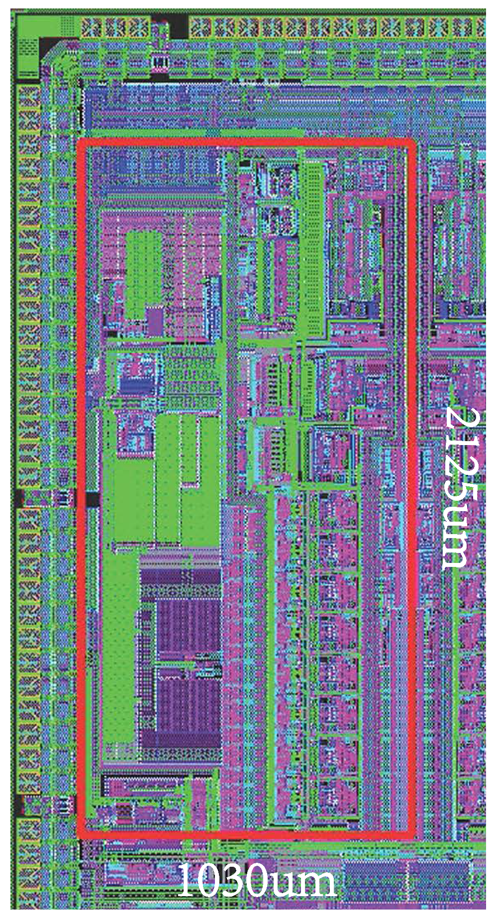
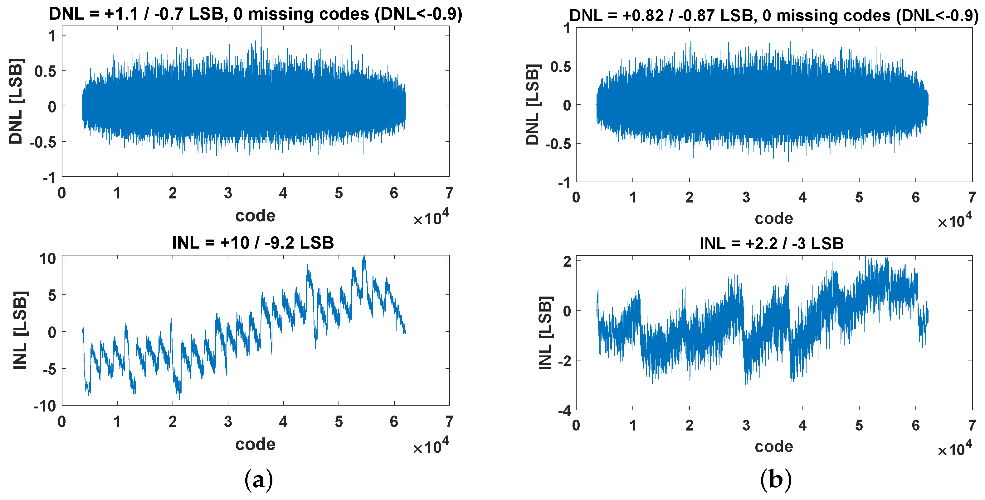
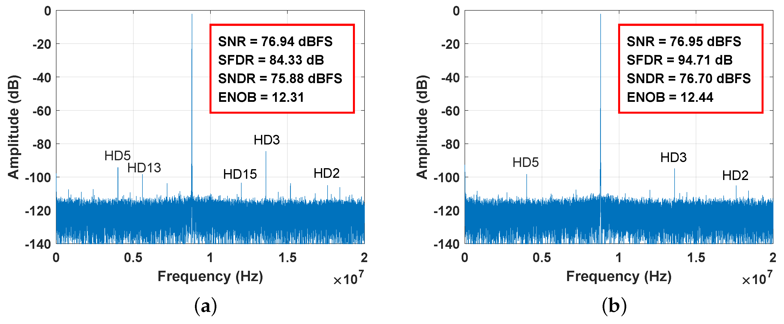
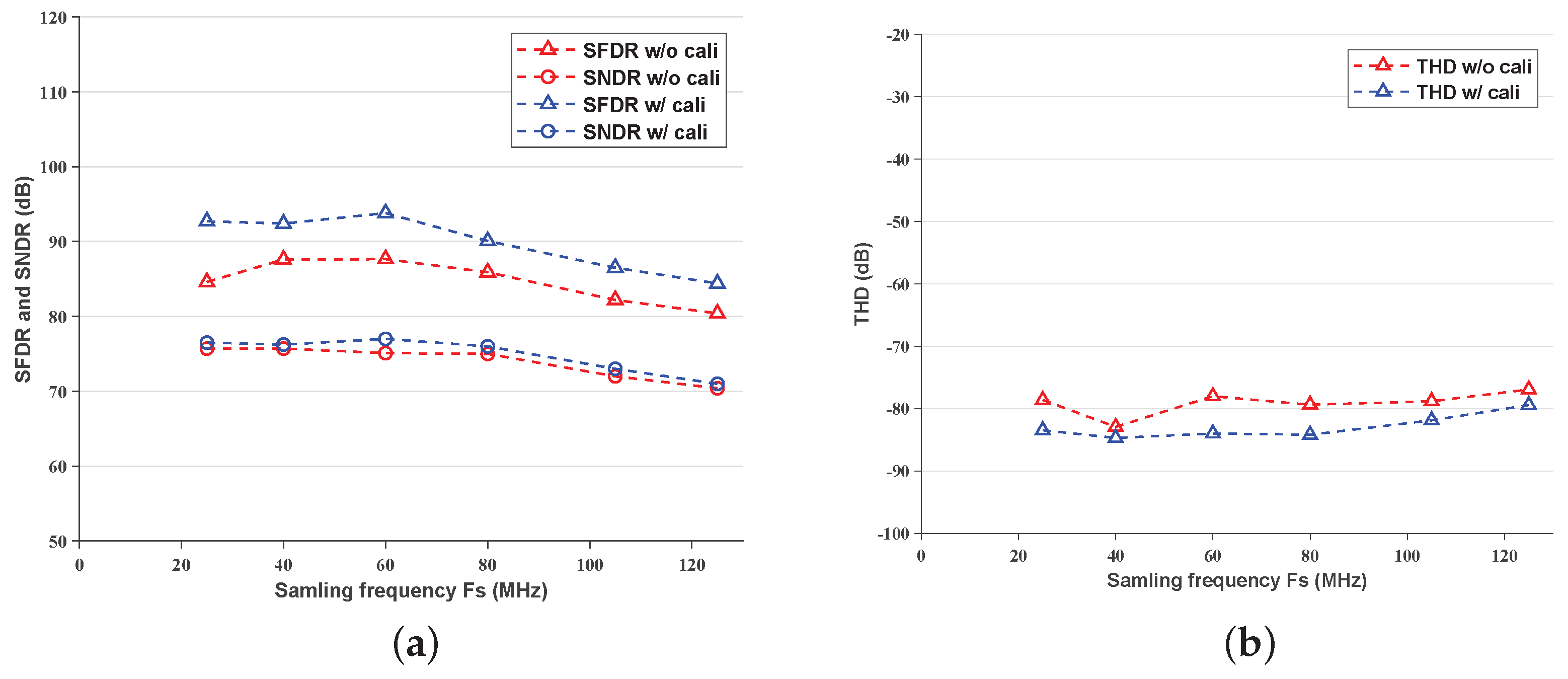
4. Measurement Results

A 16 bit SHA-less pipelined ADC with a digital foreground calibration was verified in a 0.18 μ m CMOS process. The layout is illustrated in Figure 9. It occupies an area of 1030 μ m × 2125 μ m. As shown in Figure 10, differential and integral non-linearity (DNL and INL) before calibration are in the range of −0.7/1.1 LSB and −9.2/10 LSB, which are improved to −0.87/0.82 LSB and −3/2.2 LSB, respectively. Figure 11 shows the FFT spectrum of the ADC with and without calibration while sampling a 30.5 MHz input signal with an amplitude of −2 dBFS at 40 MS/s. In addition, Figure 12a shows a plot of the dynamic performances, which depict the SNDR (signal-to-noise-plus-distortion ratio) and SFDR versus the sampling rates. Furthermore, Figure 12b shows the THD (Total Harmonic Distortion) characteristics. The results show, with the help of calibration, that the SFDR can even achieve about an 8 dB improvement at some frequency. A degradation of SFDR at a higher sampling frequency mainly originates from the imperfect settling of the ADC. The ADC consumes 154 mW of total power (reference buffer and clock included) when operating at a 1.8 V supply. The measured results are summarized in Table 2.
Table 2 compares the proposed ADC with several pipelined ADCs using different calibration techniques reported recently. As shown in the table, other methods are based on dithering or others, which need a large area and power consumption. The proposed calibration method achieves better performance with both a lower power budget and less circuit complexity. More specifically, the proposed foreground calibration approach achieves a significant reduction in power consumption by half, while simultaneously attaining a threefold decrease in area, owing to getting rid of the dedicated buffer to generate the calibration voltage. Furthermore, the SFDR of the ADC is comparable to the best results in [10], which is mainly because of the modified MADC and the proposed calibration technique.

5. Conclusions

In this brief, a 16 bit SHA-less 125 MS/s 0.18 μ m CMOS pipelined ADC with a digital foreground calibration based on capacitor reuse is presented. Combined with the modified MDAC in the first stage, no extra circuit is required except for one assistant capacitor in the second stage during the calibration mode. We avoid a common-mode voltage buffer by splitting the sampling capacitors in half, which saves the area and power overheads. The measurement results show that the proposed calibration method significantly improves the ADC performance, especially for SFDR.

Author Contributions

Conceptualization, Z.Z. and Y.H.; methodology, Z.Z.; Design, Y.H. and Z.Z.; formal analysis, Y.H. and Y.D.; measurement, Y.H., Z.Z. and L.L.; writing—original draft preparation, Z.Z.; writing—review and editing, Z.Z., Y.D., Y.H. and L.L.; supervision, Z.Z. and Y.D.; project administration, L.L. and Y.D.; funding acquisition, L.L. and Y.D. All authors have read and agreed to the published version of the manuscript.

Funding

This work is supported by the Research Foundation of Strategic Priority Research Program of Chinese Academy of Sciences (XDA18030100) and Shanghai Sailing Program (22YF1456400).

Data Availability Statement

Data are contained within the article.

Conflicts of Interest

The authors declare no conflicts of interest.

References

  1. Vecchi, D.; Mulder, J.; van der Goes, F.M.L.; Westra, J.R.; Ayranci, E.; Ward, C.M.; Wan, J.; Bult, K. An 800 MS/s Dual-Residue Pipeline ADC in 40 Nm CMOS. IEEE J. Solid-State Circuits 2011, 46, 2834–2844. [Google Scholar] [CrossRef]
  2. Savla, A.; Leonard, J.; Ravindran, A. A Novel Queuing Architecture for Background Calibration of Pipeline ADCs. In Proceedings of the 2004 IEEE International Symposium on Circuits and Systems (IEEE Cat. No.04CH37512), Vancouver, BC, Canada, 23–26 May 2004; Volume 1, p. I. [Google Scholar]
  3. Sobhi, J.; Kanani, Z.K.; Tahmasebi, A.; Yousefi, M. A Mixed Mode Background Calibration Technique for Pipeline ADCs. In Proceedings of the 2009 4th IEEE Conference on Industrial Electronics and Applications, Xi’an, China, 25–27 May 2009; pp. 2452–2455. [Google Scholar]
  4. Sobhi, J.; Kanani, Z.K.; Tahmasebi, A.; Yousefi, M. A Simple Background Interstage Gain Calibration Technique for Pipeline ADCs. In Proceedings of the 2009 6th International Conference on Electrical Engineering/Electronics, Computer, Telecommunications and Information Technology, Kuala Lumpur, Malaysia, 3–5 April 2009; Volume 1, pp. 508–511. [Google Scholar]
  5. Lee, H.S.; Hodges, D.; Gray, P. A self calibrating 12b 12 µs CMOS ADC. In Proceedings of the 1984 IEEE International Solid-State Circuits Conference, Digest of Technical Papers, San Francisco, CA, USA, 22–24 February 1984; Volume XXVII, pp. 64–65. [Google Scholar] [CrossRef]
  6. Karanicolas, A.; Lee, H.; Bacrania, K. A 15 b 1 Ms/s digitally self-calibrated pipeline ADC. In Proceedings of the 1993 IEEE International Solid-State Circuits Conference Digest of Technical Papers, San Francisco, CA, USA, 24–26 February 1993; pp. 60–61. [Google Scholar] [CrossRef]
  7. Goes, J.; Vital, J.; Alves, L.; Ferreira, N.; Ventura, P.; Bach, E.; Franca, J.; Koch, R. A low-power 14-b 5 MS/s CMOS pipeline ADC with background analog self-calibration. In Proceedings of the 26th European Solid-State Circuits Conference, Stockholm, Sweden, 19–21 September 2000; pp. 172–175. [Google Scholar]
  8. Lee, S.H.; Song, B.S. A direct code error calibration technique for two-step flash A/D converters. IEEE Trans. Circuits Syst. 1989, 36, 919–922. [Google Scholar] [CrossRef]
  9. Song, B.S.; Tompsett, M.; Lakshmikumar, K. A 12-bit 1-Msample/s capacitor error-averaging pipelined A/D converter. IEEE J. Solid-State Circuits 1988, 23, 1324–1333. [Google Scholar] [CrossRef]
  10. Devarajan, S.; Singer, L.; Kelly, D.; Decker, S.; Kamath, A.; Wilkins, P. A 16-Bit, 125 MS/s, 385 mW, 78.7 dB SNR CMOS Pipeline ADC. IEEE J. Solid-State Circuits 2009, 44, 3305–3313. [Google Scholar] [CrossRef]
  11. Zheng, X.; Wang, Z.; Li, F.; Zhao, F.; Yue, S.; Zhang, C.; Wang, Z. A 14-Bit 250 MS/s IF Sampling Pipelined ADC in 180 Nm CMOS Process. IEEE Trans. Circuits Syst. I Regul. Pap. 2016, 63, 1381–1392. [Google Scholar] [CrossRef]
  12. Ali, A.M.A.; Dinc, H.; Bhoraskar, P.; Dillon, C.; Puckett, S.; Gray, B.; Speir, C.; Lanford, J.; Brunsilius, J.; Derounian, P.R.; et al. A 14 Bit 1 GS/s RF Sampling Pipelined ADC With Background Calibration. IEEE J. Solid-State Circuits 2014, 49, 2857–2867. [Google Scholar] [CrossRef]
  13. Hung, T.C.; Liao, F.W.; Kuo, T.H. A 12-Bit Time-Interleaved 400-MS/s Pipelined ADC With Split-ADC Digital Background Calibration in 4000 Conversions/Channel. IEEE Trans. Circuits Syst. II Express Briefs 2019, 66, 1810–1814. [Google Scholar]
  14. Jing, J.; Ding, Y.; Shen, L.; Wang, P.; Li, F. A Wide Input Common-mode Range Pipelined ADC Front-end with Common-mode Refreshing. In Proceedings of the 2023 21st IEEE Interregional NEWCAS Conference (NEWCAS), Edinburgh, UK, 26–28 June 2023; pp. 1–5. [Google Scholar] [CrossRef]
  15. Hassan, A.W.; Zhou, D.; Silva-Martinez, J. Matrix-Based Digital Calibration Technique for High-Performance SAR and Pipeline ADCs. IEEE Trans. Circuits Syst. I Regul. Pap. 2024, 71, 20–28. [Google Scholar] [CrossRef]
  16. Xue, B.; Lu, Z.; Zhang, W.; Tang, H.; Peng, X. A Sinusoidal Fitting-based Digital Foreground Calibration Technique for Pipelined ADC. In Proceedings of the 2023 IEEE 15th International Conference on ASIC (ASICON), Nanjing, China, 24–27 October 2023; pp. 1–4. [Google Scholar] [CrossRef]
  17. Jia, H.; Guo, X.; Zhai, H.; Wu, D.; Liu, X. A Noval Calibration Based on Genetic Algorithm for Pipelined ADC. In Proceedings of the 2023 IEEE 6th International Electrical and Energy Conference (CIEEC), Hefei, China, 12–14 May 2023; pp. 3223–3226. [Google Scholar] [CrossRef]
  18. Sun, L.; Zhang, Z.; Lang, L.; Kang, T.; Xiong, W.; Liu, Y.; Zhong, W.; Dong, Y. An Adaptive and Universal Timing Mismatch Estimation Method for TIADCs. IEEE Trans. Very Large Scale Integr. (VLSI) Syst. 2023, 31, 1614–1618. [Google Scholar] [CrossRef]
  19. Kang, T.; Zhang, Z.; Xiong, W.; Sun, L.; Liu, Y.; Zhong, W.; Lang, L.; Shan, Y.; Dong, Y. A Digital Timing-Mismatch Calibration Technique for Time-Interleaved ADCs Based on a Coordinate Rotational Digital Computer Algorithm. Electronics 2023, 12, 1319. [Google Scholar] [CrossRef]
  20. Li, J.; Moon, U.K. Background calibration techniques for multistage pipelined ADCs with digital redundancy. IEEE Trans. Circuits Syst. II Analog Digit. Signal Process. 2003, 50, 531–538. [Google Scholar] [CrossRef]
  21. Taherzadeh-Sani, M.; Hamoui, A. Digital Background Calibration of Capacitor-Mismatch Errors in Pipelined ADCs. IEEE Trans. Circuits Syst. II Express Briefs 2006, 53, 966–970. [Google Scholar] [CrossRef]
  22. Shi, L.; Zhao, W.; Wu, J.; Chen, C. Digital Background Calibration Techniques for Pipelined ADC Based on Comparator Dithering. IEEE Trans. Circuits Syst. II Express Briefs 2012, 59, 239–243. [Google Scholar] [CrossRef]
  23. Murmann, B.; Boser, B. A 12-bit 75-MS/s pipelined ADC using open-loop residue amplification. IEEE J. Solid-State Circuits 2003, 38, 2040–2050. [Google Scholar] [CrossRef]
  24. Hung, L.H.; Lee, T.C. A Split-Based Digital Background Calibration Technique in Pipelined ADCs. IEEE Trans. Circuits Syst. II Express Briefs 2009, 56, 855–859. [Google Scholar] [CrossRef]
  25. Chang, D.Y.; Moon, U.K. Radix-based digital calibration technique for multi-stage ADC. In Proceedings of the 2002 IEEE International Symposium on Circuits and Systems (ISCAS), Phoenix-Scottsdale, AZ, USA, 26–29 May 2002; Volume 2, p. II. [Google Scholar] [CrossRef]
  26. Kaur, J.; Prabhakar, P.; Singh, A.; Agarwal, A. Fast digital foreground gain error calibration for pipelined ADC. IET Circuits Devices Syst. 2019, 13, 219–225. [Google Scholar] [CrossRef]
  27. Devarajan, S.; Singer, L.; Kelly, D.; Pan, T.; Silva, J.; Brunsilius, J.; Rey-Losada, D.; Murden, F.; Speir, C.; Bray, J.; et al. A 12-b 10-GS/s Interleaved Pipeline ADC in 28-Nm CMOS Technology. IEEE J. Solid-State Circuits 2017, 52, 3204–3218. [Google Scholar] [CrossRef]
Figure 1. Traditional 2.5-bit MDAC (a) and its transfer curve in the first stage (b).
Electronics 13 01474 g001
Figure 2. The output results of the pipelined ADC with capacitor mismatch.
Electronics 13 01474 g002
Figure 3. Proposed 16 bit SHA-less pipelined ADC architecture.
Electronics 13 01474 g003
Figure 4. Modified MDAC in the first stage.
Electronics 13 01474 g004
Figure 5. In a normal conversion mode, the switching method of the modified MDAC in the sampling phase φ 1 (a) and holding phase φ 2 (b). The two clock phases φ 1 and φ 2 are non-overlapping.
Electronics 13 01474 g005
Figure 6. The first two stages’ amplifier in a calibration mode to generate the calibration voltage 1 2 V r e f ; (a) sampling phase φ c1, (b) holding phase φ c2.
Electronics 13 01474 g006
Figure 7. The first two stages’ amplifier in calibration mode to estimate the C4 error code: (a) sampling phase φ c1, (b) holding phase φ c2.
Electronics 13 01474 g007
Figure 8. The flowchart of the proposed calibration.
Electronics 13 01474 g008
Figure 9. The layout of the ADC.
Electronics 13 01474 g009
Figure 10. Measured DNL and INL of the ADC. Before (a) and after calibration (b).
Electronics 13 01474 g010
Figure 11. Measured spectrum of the ADC output at 40 MS/s for an input frequency of 30.5 MHz at −2 dBFS. Before (a) and after calibration (b).
Electronics 13 01474 g011
Figure 12. Measured dynamic performances at a 10.5MHz input signal frequency with and without calibration. SFDR and SNDR (a) and THD (b).
Electronics 13 01474 g012
Table 1. Switching method to calculate the error(i) caused by a capacitor mismatch.
Err(i) C i Switch to V R P C i Switch to V RN Capacitor Switched Code of C 7 - C 0
01~30, 4~700001110
10, 2~31, 4~700001101
20~1, 32, 4~700001011
i=30~23~700000111
40~45~700011111
50~3, 54, 6~700101111
60~3, 64~5, 701001111
70~3, 74~610001111
Table 2. Performance comparison with state-of-the-art ADCs.
Specification[10][11][14] 1This Work
Process (nm)180180180180
Fs (MHz)125250125125
Resolution (Bits)16141616
SFDR (dBFS)9287.990.794.7
SNDR (dBFS)78.668.279.576.7
DNL/INL (LSBs)0.6/3.00.15/1-/-0.8/3.0
Power (mW)38530058.6 2154
Area (mm2)66-2.19
1 Simulation results. 2 The power of front-end stages.
Disclaimer/Publisher’s Note: The statements, opinions and data contained in all publications are solely those of the individual author(s) and contributor(s) and not of MDPI and/or the editor(s). MDPI and/or the editor(s) disclaim responsibility for any injury to people or property resulting from any ideas, methods, instructions or products referred to in the content.

