Article

DSASPP: Depthwise Separable Atrous Spatial Pyramid Pooling for PCB Surface Defect Detection

Information Engineering College, Henan University of Science and Technology, Luoyang 471000, China
*
Author to whom correspondence should be addressed.
Electronics 2024, 13(8), 1490; https://doi.org/10.3390/electronics13081490
Submission received: 21 March 2024 / Revised: 7 April 2024 / Accepted: 10 April 2024 / Published: 14 April 2024

Abstract

:
Printed circuit board (PCB) defect detection is an important and indispensable part of industrial production. PCB defects, due to the small target and similarity between classes, in the actual production of the detection process are prone to omission and false detection problems. Traditional machine-learning-based detection methods are limited by the actual needs of industrial defect detection and do not show good results. Aiming at the problems related to PCB defect detection, we propose a PCB defect detection algorithm based on DSASPP-YOLOv5 and conduct related experiments on the PKU-Market-PCB dataset. DSASPP-YOLOv5 is an improved single-stage detection model, and we first used the K-means++ algorithm for the PKU-Market-PCB dataset to recluster the model so that the model is more in line with the characteristics of PCB small target defects. Second, we design the Depthwise Separable Atrous Spatial Pyramid Pooling (DSASPP) module, which effectively improves the correlation between local and global information by constructing atrous convolution branches with different dilated rates and a global average pooling branch. The experimental results show that our model achieves satisfactory results in both the mean average precision and detection speed metrics compared to existing models, proving the effectiveness of the proposed method.

1. Introduction

Industrial internet is the core cornerstone of the fourth industrial revolution [1], so in the field of electronics manufacturing, printed circuit board (PCB) as a variety of components connected to the important parts [
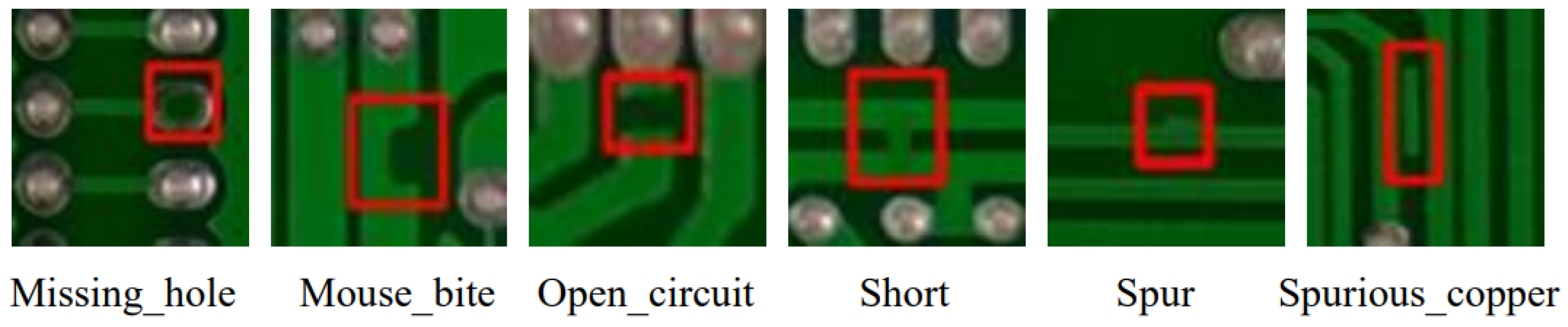
2], its quality plays a vital role in the quality of electronic products integrated by it. In recent years, the density and complexity of PCB have been increasing, and the production process of PCB is also gradually becoming more cumbersome. PCB in industrial production often has various defects, such as open circuit, short, missing holes, mouse bite, spur, spurious copper [3], etc. These defects, if not found and dealt with in a timely manner, will affect the subsequent assembly and debugging processes and even cause the failure of the entire product. Therefore, PCB surface defect detection is a key link in the electronic manufacturing process, and its quality directly affects the service life and reliability of electronic products [4].
The methods used in the field of industrial defect detection are categorized into traditional methods and vision-based detection methods. Traditional methods mainly include manual visual detection [5] and functional testing [6], while traditional methods are characterized by low efficiency, slow detection speed, and difficulty in identifying similar defective targets, so they are not suitable for applications in large-scale industrial scenarios, and fast and accurate vision-based detection methods occupy the mainstream at present [7]. Vision-based industrial defect detection not only has important research value but also offers many potential applications. The traditional machine learning approaches include support vector machines [8], decision trees [9], and genetic algorithms [10], etc., but the traditional machine learning approaches in the domain of industrial defect detection are affected by the diversity of the defects and their weaknesses; the detection effect is poor.
Recent advances in deep learning have led to more mature applications for deep-learning-based visual detection methods, including two-stage detection algorithms R-CNN [11], Fast R-CNN [12], Faster R-CNN [13], and Mask R-CNN [14], etc.; as well as single-stage detection algorithms SSD [15] and YOLO [16,17,18,19] series, etc.
Zhang et al. [20] learned the high-level features present in the defects by using VGG-16 as a base network, and the authors evaluated SVM in combination with LBP and HOG features, respectively, demonstrating the superior performance of deep feature learning; Xie et al. [21] introduced a multilevel residual mixed-attention module for feature learning in the YOLOv4 network to improve the shallow network’s capacity for feature representation and focus more attention toward object features while reducing the interference of irrelevant features; Adibhatla et al. [22] used a miniature YOLOv2 network improved by YOLOv1 in order to achieve faster PCB defect detection and obtained good detection accuracy on 11,000 images of 11 types of defects; Ding et al. [23] learned a similarity measure between image pairs by designing a Siamese network fusing multi-scale deep features. During the training phase, the authors applied a contrast loss function to optimize the feature extraction network by utilizing the distance between pairs of picture vectors. The described multi-scale model offers a good solution for the defect detection problem and outperforms the single-scale feature structure. Single-stage detection approaches such as YOLO do not require additional candidate region generation [24], which simplifies the complexity of the target detection procedure and converts the issue into a straightforward regression problem when compared to two-stage candidate region-based detection approaches, simplifies the process of target detection, accelerates the speed of defective target detection, and is more suitable for industrial scenarios, so this paper selects YOLOv5 [25] as a baseline model for single-stage detection algorithms.
As the production of PCB currently tends to be thin and light and densification, the density of its wiring and welding is increasing day by day [26]. While the defects on the surface of the PCB have a small target area and the background is complex in industrial scenarios, the defects and the background are easily confused and it is not easy to differentiate between them, with a high rate of misdetection and omission and a poor effect of detection. For the purpose of meeting the demand for accuracy in PCB surface defect detection in industrial situations, this paper proposes a PCB surface defect detection algorithm based on DSASPP-YOLOv5, with the following two main contributions:
  • Utilize the K-means++ clustering algorithm to re-cluster the initial anchor box parameters and adopt 1-IoU as the distance metric to enhance the model’s capacity to detect defective targets in smaller areas;
  • In this paper, we design and propose the Depthwise Separable Atrous Spatial Pyramid Pooling (DSASPP) module, which constructs atrous convolution branches with different dilated rates and global average pooling branches to improve the correlation between local and global information. We also introduce depthwise separable convolution using the Gaussian error linear Unit (GELU) as activation function in atrous convolution blocks to balance precision and number of parameters.

2. Methods

2.1. DSASPP-YOLOv5 Network

This study makes improvements based on the YOLOv5 network model, and Figure 1 displays the improved model’s structure. The original YOLOv5 model itself has excellent detection capability, but the detection accuracy of the model still requires improvement for PCB defective targets that are small in size and easy to confuse with the background. This study uses the K-means++ approach to re-cluster the nine initial anchor values of YOLOv5 in order to precisely locate and identify the target information in the effective region. The re-clustered anchors are more in line with the feature distribution characteristics of the PCB surface defect dataset, so the model is more effective in capturing and extracting the target region information; In order to strengthen the backbone network part’s feature extraction ability for defective targets, improve the network’s anti-interference capability for unimportant background information, and enhance the network’s detection accuracy, this paper designs the DSASPP module and introduces it into the YOLOv5 backbone network in order to make full fusion of multiscale contextual information to get better detection effects and to make misdetection and omission of detection effectively controlled.

2.2. K-Means++ Clustering Algorithm

There are three prediction branches in the YOLOv5 network model, and nine different sizes of anchor values (anchors: 10, 13; 16, 30; 33, 23; 30, 61; 62, 45; 59, 119; 116, 90; 156, 198; 373, 326) are set by default, which are applied to the three separate feature map scales for the purpose of predicting the target bounding box. Since the YOLOv5’s default anchor set is derived from the K-means clustering approach on the PASCAL VOC dataset with a size of 608 × 608 , it is only applicable to feature maps with a more uniform scale size and a larger target detection area. In this study’s PCB surface defects dataset, the location of various types of PCB defects is not fixed, the target size is more extreme, and most of them are small targets and use the 640 × 640 size of the image as the input, so the preset anchor value of YOLOv5 is not applicable to the content of the research in this paper.
The first task of the K-means clustering method is the initial procedure to complete initializing all k cluster centers, and its convergence is extremely dependent on the cluster centers’ initialization state. Consequently, there is a significant risk of running into the local optimum problem when clustering using the K-means clustering method. Compared with the traditional K-means clustering method, the K-means++ [27] algorithm improves the effectiveness of clustering by optimizing the choice of the initial cluster centers.Under comprehensive consideration, this paper adopts the K-means++ clustering algorithm to re-cluster the anchor box in the PCB surface defects dataset. Intersection over Union (IoU) calculates the overlap between the bounding box and the ground truth. We take the maximum IoU as a reference and use the value of 1-IoU instead of Euclidean distance as a distance metric. The distance is calculated as in Equation (1), where b o x is the true labeled box in the dataset, and c e n t r o i d is the centroid of the clusters. By recalculating the distance between each cluster, the clustering accuracy of this paper is finally improved.
D ( b o x , c e n t r o i d ) = 1 I o U
The process of the K-means++ clustering algorithm is shown below:
  • A sample point is chosen at random from the project dataset as the first initial clustering center C i ;
  • Define the farthest distance between each sample point and the current existing clustering center as D ( x ) . As shown in Equation (2), the probability of each sample point being selected as the next clustering center is defined as P ( x ) , and in this paper, we use the roulette wheel method to select a new clustering center C i based on the size of the probability P ( x ) .
  • Repeat process 2. until k clustering centers are selected.
P ( x ) = D ( x ) 2 x X D ( x ) 2

2.3. DSASPP Module

For the purpose of better improving the correlation between local and global information, DeepLabV2 [28] proposes an atrous spatial pyramid pooling (ASPP) structure. The atrous convolution and pooling structure, which together make up ASPP, allow for the extraction of multi-scale features from objects with a larger receptive field while maintaining image resolution, but the module still suffers from the following shortcomings:
  • Using the same dilation rate consecutively or using a set of dilation rate values with a common factor relationship other than 1, both of which may cause “Gridding Effect” and result in local information loss;
  • The ReLU function used in the improved ASPP has certain defects, which may cause the problem of “Dying ReLU” and make some effective information lost;
  • In practice, the ASPP module often introduces a significant number of additional parameters while increasing accuracy, which is not worth the cost for industrial application scenarios with detection speed requirements.
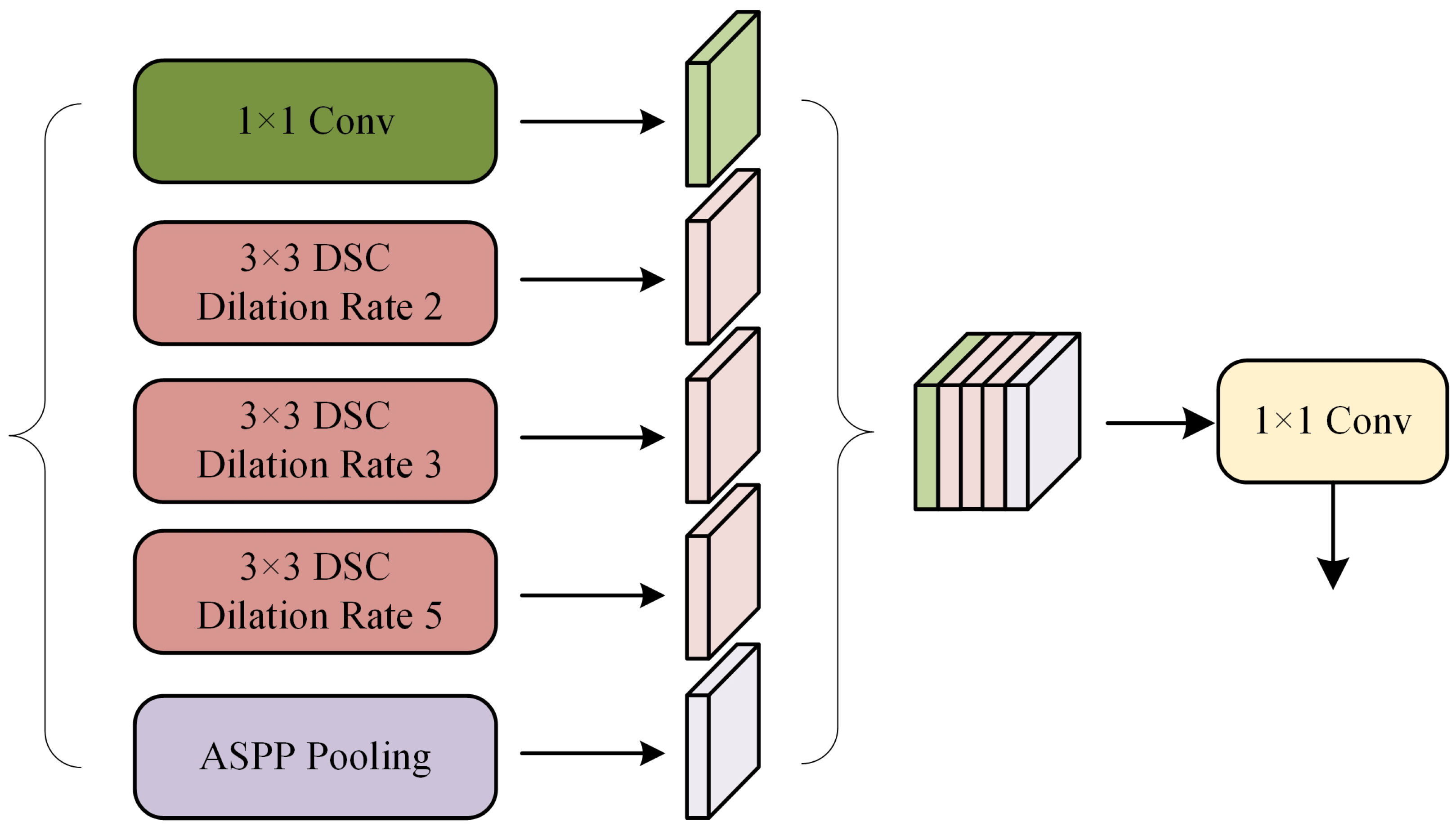
To deal with the problem that exists within the ASPP structure, we have addressed it through several works on standardized construction rules for atrous convolution, the use of the GELU activation function, and the introduction of depthwise separable convolution. Inspired by the related work in this paper, this paper proposes the DSASPP Module. As illustrated in Figure 2, the YOLOv5 model backbone network’s output feature map is initially sent into the DSASPP module, where there are three primary components to the DSASPP module:
  • The first component is the first branch, which utilizes a 1 × 1 standard convolution in order to maintain the original receptive field;
  • The second part is the second to the fourth branch, using atrous convolution with a 3 × 3 convolution kernel size and dilation rate of 2, 3, and 5 to obtain different size receptive fields while enhancing feature extraction. We decreased the total quantity of parameters in this study by introducing depthwise separable convolution, where the activation function part is chosen to be the theoretically better GELU function;
  • The third component is the fifth branch, which introduces global average pooling so as to obtain global features, improves the model’s stability and accuracy, and suppresses the overfitting phenomenon in the network.
Ultimately, the five branches of the three DSASPP modules’ components process the feature maps, which are stacked in the channel dimension after that, and then processed by the standard convolution of 1 × 1 to make the information at different scales fully integrated.

2.3.1. Atrous Convolution

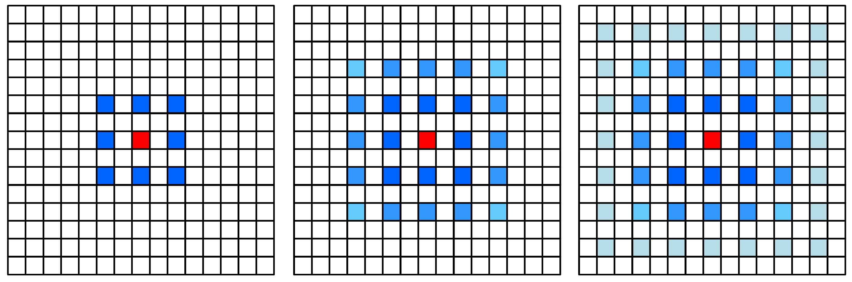
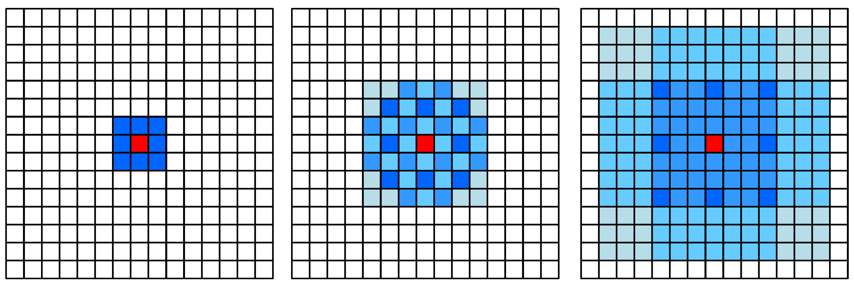
It has been found that the practice of successive atrous convolution at the same dilation rate to obtain the same spatial resolution fills zero between the expanded pixels of the convolution kernel, but the model only samples the locations with non-zero values, thus losing local information and generating the “Gridding” problem, also known as the “Gridding Effect”, as illustrated within Figure 3. The reasonable dilation rate is set as shown in Figure 4. Wang and others [29] proposed the concept of hybrid dilated convolution (HDC), which aims to enable the receptive field’s final size to completely cover a square region with no empty or missing edges after a sequence of convolution processes. Thus, it specifies the standardized construction rule of the atrous convolution:
  • The dilation rate of different layers should not have a common factor relationship other than 1, otherwise the problem of the “Gridding Effect” at higher levels remains;
  • Define “the maximum distance between two non-zero values” as M i :
M i = max [ r i , M i + 1 2 r i , M i + 1 2 ( M i + 1 r i ) ]
As shown in Equation (3), where M i stands for the maximum distance in the i-th layer between two non-zero values and r i is the i-th layer’s dilation rate, for the last layer, the maximum distance M n should be equal to the size of r n . Assuming k i is the actual convolution kernel’s size, for n atrous convolution layers, our design goal is to make M i k i , that is, to require that the maximum distance between two non-zero elements in each layer is less than or equal to the actual convolution kernel’s size in that layer.
Considering the characteristics of the PCB surface defect dataset, this study confirms the impacts of different combinations of dilation rate of the model performance after experiments and finally designs the ASPP module based on the dilation rate combinations of 1, 2, 3, and 5.

2.3.2. GELU Activation Function

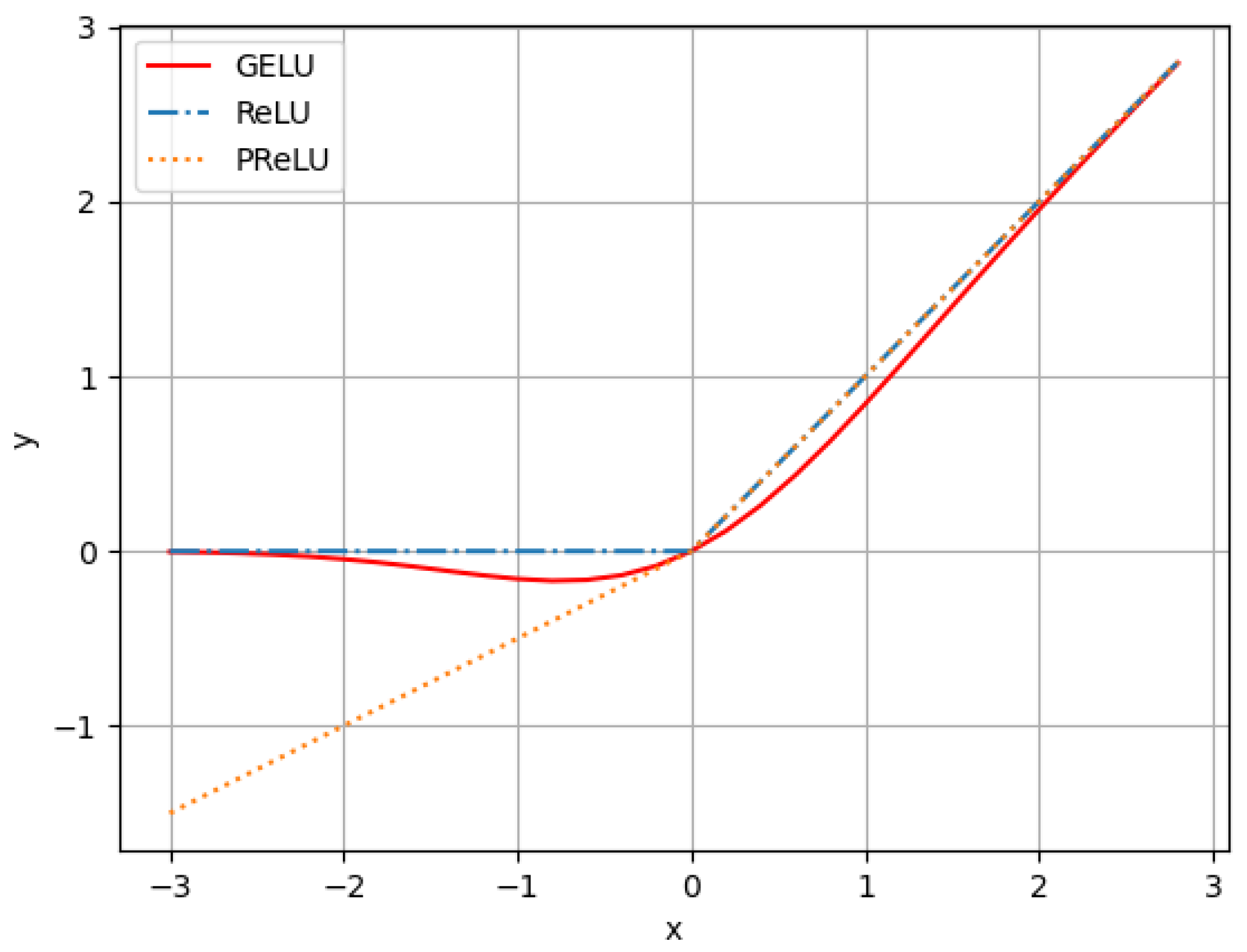
The activation function can help the model fit the training data better. ReLU is a common and critical activation function in various studies of neural networks, but the ReLU function has certain shortcomings in practical use.
The image of the ReLU function is shown in Figure 5. Since the gradient of the ReLU function is zero at x < 0 , this directly leads to the negative gradient being directly set to zero in the ReLU function, and this neuron will probably not be activated by the data in the subsequent training, and when this happens, the neuron that cannot be activated will be zero forever in the subsequent gradient change, which also shows the situation of “Dying ReLU” and will not respond to any data, making the effective information partially lost.
Based on this, some authors [30] proposed the Parametric Rectified Linear Unit (PReLU) with self-learning capability as the activation function to alleviate the problems of ReLU function, while in this paper, Gaussian Error based the GELU [31] is used as the activation function of the ASPP module. The expression of the GELU function can be approximated as Equation (4), and the comparative images of activation functions are shown in Figure 5.
G E L U ( x ) = 0.5 x ( tanh ( 2 π ( x + 0.044715 x 3 ) ) + 1 )
Compared to the ReLU function, although the PReLU function solves the problem of dead neurons by introducing a learnable parameter in the negative part of the function, it can be seen from the function images that the nonlinearities of the ReLU function and the PReLU function itself are obtained due to the segmentation function itself, and thus they are both non-frivolous at the zeros, which will have a certain impact on the network’s performance. The GELU function introduces the stochastic regularization idea compared with ReLU and similar functions, the GELU function is smoother at the zero point; it not only increases the nonlinearity of the network but can also inhibit the overfitting phenomenon of the network, so that the network converges faster; and it can also avoid the problem of dead neurons.

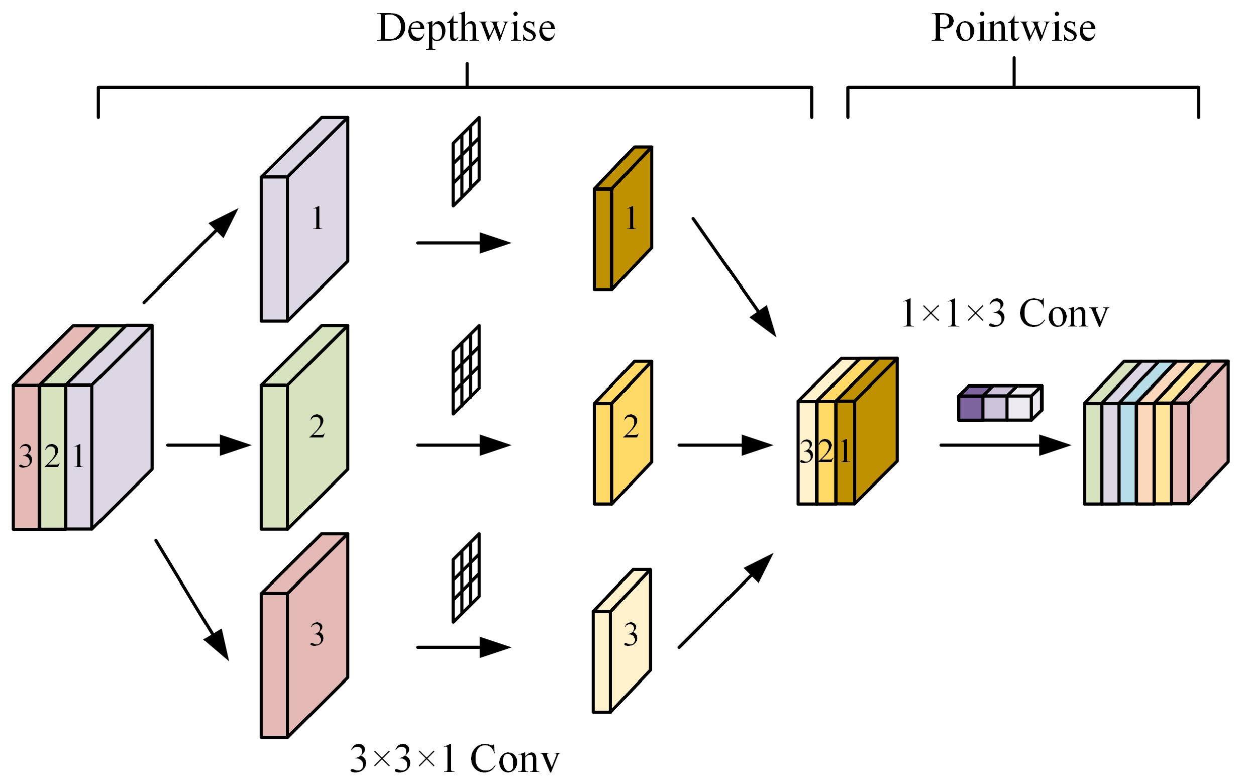
2.3.3. Depthwise Separable Convolution

In order to better meet the lightweight requirements of models in industrial scenarios based on the standard convolution operation, the literature [32] first proposed a more efficient separable convolution (SC) to decrease the model’s parameters and computational effort, which is usually utilized in neural networks in the form of depthwise separable convolution (DSC) [33,34]. Depthwise separable convolution provides a new way of thinking about convolution by decomposing the normal convolution process into two components: depthwise (DW) convolution and pointwise (PW) convolution.
As illustrated within Figure 6, the idea of depthwise convolution procedure is to split the convolution kernel in the form of a single channel, perform the convolution of a single channel separately, and then stack them together so that not only the convolution operation can be performed separately for each channel but also maintain the input feature map’s depth. After the depthwise convolution procedure, we get the output feature map with an equal number of channels given the input feature map. After that, the pointwise convolution operation, which is 1 × 1 convolutions, is performed to raise and lower the feature map’s dimension, and the output channels of the depthwise convolution operation are projected onto the new channel space.
As for the input feature map of size H × W × M and convolution kernels of size k × k , the computational effort f 1 of the standard convolution is given by Equation (5):
f 1 = H × W × k × k × M × N
where H × W denotes the size of the input feature map, k denotes the convolution kernel size, M indicates the input channel’s number, and N indicates the output channel’s number.
A similar analysis taken for depthwise separable convolution shows that the computational effort f 2 of the depthwise convolution operation and the pointwise convolution operation is shown in Equation (6):
f 2 = H × W × k × k × 1 × M + H × W × 1 × 1 × M × N
The ratio of computation of depthwise separable convolution to standard convolution is Equation (7):
f 2 f 1 = H × W × k × k × 1 × M + H × W × 1 × 1 × M × N H × W × k × k × M × N = 1 N + 1 k × k
From Equation (7), it can be seen that when the convolution kernel size k is 3, the utilization of depthwise separable convolution might decrease nearly 90% of the computation, thus achieving the purpose of model light-weighting. In this paper, we introduced depthwise separable convolution for light-weighting in the ASPP module and obtained significant results to improve the computational efficiency without significantly degrading the model performance.

3. Experimental Results and Analysis

3.1. Experimental Environment

This experiment was built based on the PyTorch deep learning framework, with a PyTorch version of torch 1.11.0 and a Python version of 3.8.16. The CPU model was Intel Core i5-12400F, and the GPU model was NVIDIA GeForce RTX3060Ti with 8GB of video memory, using single card training mode and GPU acceleration via CUDA11.3.
This experiment makes use of the open dataset of PCB defect detection released by the Intelligent Robotics Open Laboratory of Peking University (PKU-Market-PCB). The original images of this dataset total 693, and there are 6 defect categories, namely Missing_hole, Mouse_bite, Open_circuit, Short, Spur, and Spurious copper, and the sample defect images are shown in Figure 7.
Due to the difficulty of collecting industrial datasets, the dataset used in this experiment has the problem of being too small. Based on this, this experiment uses data enhancement to expand the dataset, such as randomly rotating, scaling, mirroring, brightness adjustment, and Gaussian filtering operations on the original data, so that the dataset is expanded five times; there are a total of 4158 images after the expansion, and the expanded dataset is displayed within Table 1. To better carry out the independence experiment, the dataset is randomly split into training and test sets in an 8:2 ratio, of which 3300 pictures are within the training set and 858 pictures are within the test set.

3.2. Evaluation Metrics

In this study, the evaluation metrics used in the experiments related to PCB surface defect detection are the precision rate (P), recall rate (R), mean average precision (mAP), number of parameters, and frames per second (FPS), which are commonly used as the main evaluation metrics. The specific formulas are shown in Equations (8)–(11).
P = T P T P + F P
R = T P T P + F N
A P = 0 1 P ( r ) d r
m A P = i = 0 n A P ( i ) n
where T P (True Positive) denotes the target’s numbers that were actually detected correctly, F P (False Positive) denotes the target’s numbers that were actually detected erroneously, and F N (False Negative) denotes the target’s numbers that were overlooked. The precision rate P is defined as the ratio of the number of correct ones predicted by the network model to the whole number, and the recall rate R is defined as the ratio of the number of true ones predicted by the network model to the whole number of true ones. A P is the region that the P-R curve encloses and the coordinate system, while m A P measures how well a trained model acts on the full range of categories. m A P is also used as the main evaluation metric for the target detection task. The m A P can be specifically categorized into mAP_0.5, which is the m A P at the 0.5 IoU threshold, and mAP_0.5:0.95, which is the mean m A P across a range of IoU thresholds (0.5 to 0.95 in steps of 0.05).

3.3. Model Performance Evaluation

3.3.1. K-Means++ Clustering Result Analysis

Figure 8 shows the distribution of defective target aspect ratios in the PCB surface defect dataset, and as seen in the figure, the target box dimension’s width and height in the dataset used in this study are mainly concentrated in the intervals of [0∼40, 0∼40]. The resulting intervals also demonstrate that most of the targets in the PCB surface defect dataset are small and that the preset anchor box sizes in the original YOLOv5 are not applicable to the needs of the PCB defect dataset. Figure 9 displays the effects of using the K-means++ clustering method to re-cluster the smaller targets in the PCB surface defects dataset; the clustering center’s number is set to 9. After many iterations of the genetic algorithm, all the data points in the final image are clustered into 9 regions labeled with different colors, where the yellow five-pointed stars represent the clustering centers of the regions, and the various clustering centers indicate that ultimately, we have obtained 9 combinations of different sizes of the anchor box.
In this study, we use the K-means++ clustering method to obtain the combination of anchor box sizes as displayed within Table 2, in which the feature map of 20 × 20 size is assigned with the largest three anchor box, the feature map of 40 × 40 size is assigned with the medium-sized three anchor box, and the largest feature map of 80 × 80 size is assigned with the smallest set of anchor box, which is also in line with the principle of “small targets are predicted on the large feature maps, and the large targets are predicted on the small feature maps”.

3.3.2. DSASPP Experimental Analysis

In this paper, ASPP modules with different combinations of dilation rate are tested through experiments, and as shown in Table 3, for the combinations of dilation rate that do not meet the optimal requirements for the design of atrous convolution, such as (1,2,2,2) and (1,6,12,18), there is a certain gap in the performance of the actual detection accuracy compared to that of the dilation rate combinations designed in this paper (1,2,3,5) and (1,2,3,7) due to the successive use of the same dilation rate or the presence of a common factor in the combination of the dilation rate except for 1, among which the combination of the dilation rate of (1,2,3,5) is the best performance. Combined with the characteristics of the PCB surface defect dataset, the redesigned dilation rate combination in this study effectively increases the detection accuracy of defective targets; mAP_0.5 reaches 97.23%.
Considering some of the lightweight requirements of real industrial application scenarios, experiments are carried out for the improvement of the ASPP module while maintaining the same quantity of input and output channels. From Table 4, it is evident that the ASPP module has a strong potential for capturing multi-scale information and obtains a certain degree of mAP improvement, but consequently, it increases the detection accuracy while introducing a significant number of parameters, which increases the computational burden on the model. In this paper, the Gaussian error-based GELU activation function is utilized to improve the ASPP module, and the mAP_0.5 is improved by 0.4% with only a small number of parameters added, which indicates that the GELU activation function can increase the model’s detection accuracy. On this basis, the quantity of parameters in the model is significantly decreased by 41% through the use of multi-branch depthwise separable convolution, indicating that depthwise separable convolution can effectively decrease the quantity of parameters of the ASPP module, and the improved overall model still achieves a 0.35% improvement in the mAP_0.5 compared to the unimproved ASPP module due to the GELU activation function. This paper’s improvement of the ASPP module decreased the number of parameters while increasing detection accuracy, and it verified the excellent performance of the DSASPP module in capturing multi-scale target context information.

3.4. Ablation Experiments

To confirm the model’s actual performance as described in this study, considering the actual needs of industrial defect detection, the more lightweight YOLOv5 model is selected for the benchmark model within this study, and ablation experiments are conducted on the PCB defect dataset. As shown in Table 5, where YOLOv5 represents the original model; DA is the data augmentation method used in this study; K-means++ is the anchor box clustering method used in this paper, which is used to re-cluster for the training dataset; and DSASPP indicates the Depthwise Separable Atrous Spatial Pyramid Pooling module designed in this paper.
The experimental results presented in Table 5 display that the training model with the data augmentation method used in this paper performs better than the original YOLOv5 benchmark model without data augmentation, with improvements of 0.97% and 1.05% in precision rate and mAP_0.5, respectively. After that, the dataset used in this paper was re-clustered by the K-means++ anchor box clustering algorithm, which effectively improved the model’s detection accuracy, leading to an increase in the model’s precision rate, recall rate, and mAP_0.5 of 1.31%, 1.11%, and 1.08%, respectively. Finally, the effectiveness of the DSASPP module in capturing multi-scale contextual information is demonstrated by the introduction of the DSASPP module, which reached 99.15%, 96.56%, and 98.62% for precision rate, recall rate, and mAP_0.5, respectively. Compared to the original YOLOv5 benchmark model without data augmentation, the overall model designed in this study achieved a 2.71% enhancement in the mAP_0.5 metric, and the best performance in both precision rate and recall rate with a 2.85% and 1.16% improvement, respectively, which proves the advancement of this paper’s method. From the experimental data of the ablation experiments, it is evident that the model in this paper is able to realize an accurate target detection and recognition function.

3.5. Comparison with Other Models

To validate the benefits and disadvantages of this study’s algorithm compared to other advanced algorithms in the same field, the proposed method is compared and experimented with algorithms such as Faster-RCNN [35], EfficientNet [36], MobileNetV2 [37], and YOLOv3 [38] on a PCB defect detection dataset. The quantity of parameters in the model, mAP_0.5, and FPS are utilized as the evaluation indexes of the model performance. To guarantee the experiment’s fairness, each model within the comparison experiment has the same image input size and the parameter settings are kept the same, and the best weight files of the above models are selected in the model validation for comparison on the test set, and Table 6 also displays the experimental results.
Upon examination of Table 6’s data, it is evident that the results of the comparison experiments show that this paper’s method has a greater advantage in the quantity of parameters compared with the models of Faster-RCNN (VGG16), Faster-RCNN (EfficientNet), Faster-RCNN (MobileNetV2), and YOLOv3; the mean average precision improved by 5.15%, 7.58%, 7.14%, and 3.4%, respectively; and the speed of detecting images per second improved by 85.18 frames, 72.86 frames, 76.71 frames, and 71.13 frames, respectively. The comprehensive performance of this paper’s model clearly has a significant advantage; not only has the mean average precision been improved to varying degrees, but the inference is also faster. In contrast to the CSPNet-based original YOLOv5 model, the improved model in this paper improved the mean average precision by 2.71%. However, due to an increase in model complexity, the quantity of parameters in the model increased by 28.3%, and the detection speed decreased by 10.84 frames. Despite the fact that the detection speed has somewhat decreased, the model designed in this paper can achieve better detection results under the premise of close to 100 frames per second, to satisfy the needs of industrial PCB defect detection, and the focus is to improve the defect detection precision, which is more crucial for the high-quality production of PCB, demonstrating the effectiveness of this paper’s method for the application of PCB surface defect detection.

3.6. Validation and Visualization

Figure 10 displays the visualized detection effects of the original YOLOv5 model and the model used within this study on the PKU-Market-PCB dataset, which shows the detection results of Mouse_bite, Short, Missing_hole, Spur, Open_circuit, and Spurious_copper.
By comparing the two models’ detection effects prior to and following the improvement, it can be found that the original YOLOv5 model’s precision rate level for the prediction of PCB surface defects is not high; it is prone to miss the detection of defects, especially for detecting the smaller defects in the six types of PCB surface defects, such as Spur and Spurious_copper, whose detection effect is even worse. This paper’s improved model has an exhaustive leading edge for the detection of six types of PCB surface defects, has a high precision rate in the prediction, and is able to detect defects not detected by the original model. The model in this paper improves the mean average precision, solves the problem of omission of some of the targets that are highly similar to the background, and has the value of practical application.
As seen in Figure 11, the mean average precision curves trained by this paper’s model and the unimproved YOLOv5 model are plotted as a comparison image by visualizing the data of the training process. The comparison shows that the mean average precision of this paper’s model has better performance and is basically in the convergence state after 50 epochs of training. The fluctuation of the curve at the late stage of training is better than that of the unimproved YOLOv5 model, which proves the strong stability of the method used in this study.

4. Conclusions

For the challenges of PCB surface defect detection difficulty and high omission rate in the industrial production process, we proposed a PCB surface defect detection method based on DSASPP through research, which improved the existing model. First, the data augmentation method improved the model’s detection accuracy. Then the dataset used in this study was re-clustered using the K-means++ clustering algorithm. Finally, the DSASPP module designed for this study is introduced into the backbone network, which is jointly optimized by the GELU activation function and the depthwise separable convolution. It not only acquires multi-scale target context information but also combines local and global information, which effectively improves the model’s detection effect.
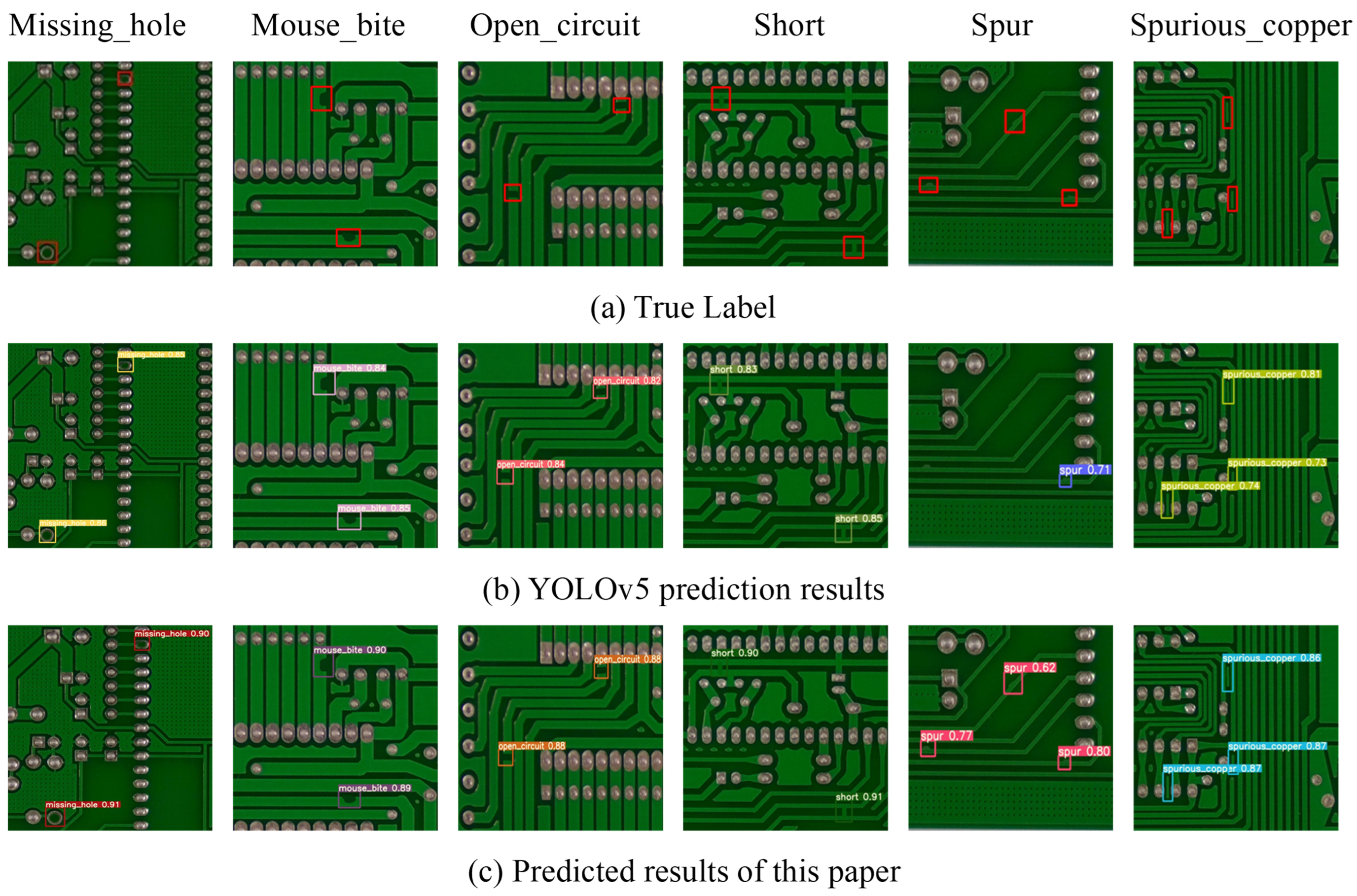
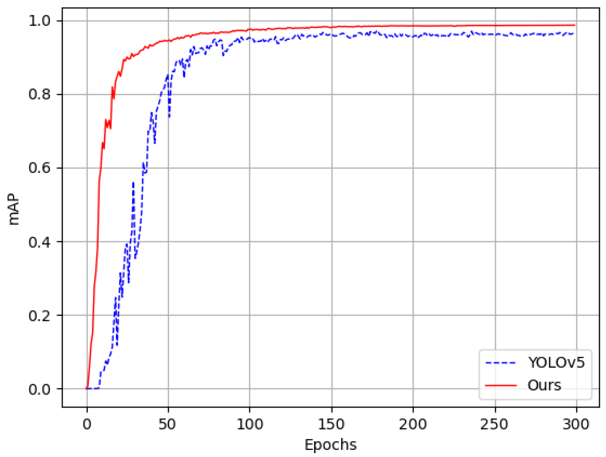
Experiments are conducted in this paper to evaluate the model against other neural network models in the same field. According to the results of the ablation experiment and comparison experiment of the model, the improved model in this study has different degrees of lead in the mean average precision index compared to other models. At the expense of several parametric quantities and computational effort, the model in this study obtains a 2.85%, 1.16%, and 2.71% improvement in precision rate, recall rate, and mAP_0.5, respectively, when compared to the unimproved YOLOv5 model. The final model is capable of detecting defects at nearly 100 frames per second, making it meet the requirements of industrial defect detection. Overall, the experiments conducted in this study demonstrate that our model has excellent comprehensive performance and can realize accurate detection and recognition tasks.
Due to the existence of limitations in time and hardware cost, the relevant experiments in this paper are conducted on a limited number of PKU-Market-PCB datasets. Despite the expansion using the data augmentation method, the dataset is not rich enough in samples, and the generalization ability of the model needs to be strengthened. Considering that the samples collected in real application scenarios are affected by the environment and other factors, detection is more difficult compared to the laboratory environment. In addition to this, although the detection precision of the method in this paper has improved, the detection speed needs to be optimized with the increase in model complexity and number of parameters.
We will later try to prune unimportant channels in the network to train PCB defect detection models with fewer parameters, a smaller size, and faster detection. In order to better improve the detection effect of the algorithms in this paper under real industrial scenarios, we are prepared to travel to real industrial environments in our subsequent work, use small portable devices for image acquisition, and carry out the task of real-time PCB defect detection.

Author Contributions

Conceptualization, Y.X. and H.H.; methodology, Y.X. and H.H.; software, Y.X. and H.H.; validation, Y.X. and H.H.; formal analysis, Y.X. and H.H.; investigation, Y.X. and H.H.; resources, Y.X. and H.H.; data curation, Y.X. and H.H.; writing—original draft preparation, Y.X. and H.H.; writing—review and editing, Y.X. and H.H.; visualization, Y.X. and H.H.; supervision, H.H.; project administration, H.H.; funding acquisition, H.H. All authors have read and agreed to the published version of the manuscript.

Funding

This research was funded by the National Natural Science Foundation of China under grant number 61672210, the Major Science and Technology Program of Henan Province under grant number 221100210500, the Central Government Guiding Local Science and Technology Development Fund Program of Henan Province under grant number Z20221343032.

Data Availability Statement

Data are contained within the article.

Conflicts of Interest

The authors declare no conflicts of interest.

References

  1. Dilberoglu, U.M.; Gharehpapagh, B.; Yaman, U.; Dolen, M. The Role of Additive Manufacturing in the Era of Industry 4.0. Procedia Manuf. 2017, 11, 545–554. [Google Scholar] [CrossRef]
  2. Ling, Q.; Isa, N.A.M. Printed Circuit Board Defect Detection Methods Based on Image Processing, Machine Learning and Deep Learning: A Survey. IEEE Access 2023, 11, 15921–15944. [Google Scholar] [CrossRef]
  3. Ding, R.W.; Dai, L.H.; Li, G.P.; Liu, H. TDD-net: A tiny defect detection network for printed circuit boards. CAAI Trans. Intell. Technol. 2019, 4, 110–116. [Google Scholar] [CrossRef]
  4. Karnik, N.; Bora, U.; Bhadri, K.; Kadambi, P.; Dhatrak, P. A comprehensive study on current and future trends towards the characteristics and enablers of industry 4.0. J. Ind. Inf. Integr. 2022, 27, 100294. [Google Scholar] [CrossRef]
  5. Li, Y.F.; Li, S.Y. Defect detection of bare printed circuit boards based on gradient direction information entropy and uniform local binary patterns. Circuit World 2017, 43, 145–151. [Google Scholar] [CrossRef]
  6. Wu, X.; Ge, Y.X.; Zhang, Q.F.; Zhang, D.L. PCB Defect Detection Using Deep Learning Methods. In Proceedings of the 24th IEEE International Conference on Computer Supported Cooperative Work in Design (IEEE CSCWD), Dalian, China, 5–7 May 2021; pp. 873–876. [Google Scholar] [CrossRef]
  7. Raj, A.; Sajeena, A. Defects Detection in PCB Using Image Processing for Industrial Applications. In Proceedings of the International Conference on Inventive Communication and Computational Technologies (ICICCT), Coimbatore, India, 20–21 April 2018; pp. 1077–1079. [Google Scholar]
  8. Lee, Y.; Lin, Y.; Wahba, G. Multicategory Support Vector Machines: Theory and Application to the Classification of Microarray Data and Satellite Radiance Data. J. Am. Stat. Assoc. 2004, 99, 67–81. [Google Scholar] [CrossRef]
  9. Rokach, L.; Maimon, O. Top-Down Induction of Decision Trees Classifiers—A Survey. IEEE Trans. Syst. Man Cybern. Part C (Appl. Rev.) 2005, 35, 476–487. [Google Scholar] [CrossRef]
  10. Doerr, B.; Huu Phuoc, L.; Makhmara, R.; Ta Duy, N. Fast Genetic Algorithms. In Proceedings of the Genetic and Evolutionary Computation Conference (GECCO), Berlin, Germany, 15–19 July 2017; pp. 777–784. [Google Scholar] [CrossRef]
  11. Girshick, R.; Donahue, J.; Darrell, T.; Malik, J. Rich feature hierarchies for accurate object detection and semantic segmentation. In Proceedings of the 27th IEEE Conference on Computer Vision and Pattern Recognition (CVPR), Columbus, OH, USA, 23–28 June 2014; pp. 580–587. [Google Scholar] [CrossRef]
  12. Girshick, R. Fast R-CNN. In Proceedings of the IEEE International Conference on Computer Vision, Santiago, Chile, 7–13 December 2015; pp. 1440–1448. [Google Scholar] [CrossRef]
  13. Ren, S.; He, K.; Girshick, R.; Sun, J. Faster R-CNN: Towards Real-Time Object Detection with Region Proposal Networks. IEEE Trans. Pattern Anal. Mach. Intell. 2017, 39, 1137–1149. [Google Scholar] [CrossRef]
  14. He, K.; Gkioxari, G.; Dollar, P.; Girshick, R. Mask R-CNN. In Proceedings of the 16th IEEE International Conference on Computer Vision (ICCV), Venice, Italy, 22–29 October 2017; pp. 2980–2988. [Google Scholar] [CrossRef]
  15. Liu, W.; Anguelov, D.; Erhan, D.; Szegedy, C.; Reed, S.; Fu, C.Y.; Berg, A.C. SSD: Single Shot MultiBox Detector. In Proceedings of the 14th European Conference on Computer Vision (ECCV), Amsterdam, The Netherlands, 8–16 October 2016; Volume 9905, pp. 21–37. [Google Scholar] [CrossRef]
  16. Redmon, J.; Divvala, S.; Girshick, R.; Farhadi, A. You Only Look Once: Unified, Real-Time Object Detection. In Proceedings of the 2016 IEEE Conference on Computer Vision and Pattern Recognition (CVPR), Las Vegas, NV, USA, 27–30 June 2016; pp. 779–788. [Google Scholar] [CrossRef]
  17. Redmon, J.; Farhadi, A. YOLO9000: Better, Faster, Stronger. In Proceedings of the 30th IEEE/CVF Conference on Computer Vision and Pattern Recognition (CVPR), Honolulu, HI, USA, 21–26 July 2017; pp. 6517–6525. [Google Scholar] [CrossRef]
  18. Redmon, J.; Farhadi, A. YOLOv3: An Incremental Improvement. arXiv 2018, arXiv:1804.02767. [Google Scholar]
  19. Bochkovskiy, A.; Wang, C.Y.; Liao, H.Y.M. YOLOv4: Optimal Speed and Accuracy of Object Detection. arXiv 2020, arXiv:2004.10934. [Google Scholar]
  20. Zhang, C.; Shi, W.; Li, X.; Zhang, H.; Liu, H. Improved bare PCB defect detection approach based on deep feature learning. J. Eng. 2018, 2018, 1415–1420. [Google Scholar] [CrossRef]
  21. Xie, H.; Li, Y.; Li, X.; He, L. A method for surface defect detection of printed circuit board based on improved YOLOv4. In Proceedings of the 2021 IEEE 2nd International Conference on Big Data, Artificial Intelligence and Internet of Things Engineering (ICBAIE), Nanchang, China, 26–28 March 2021; pp. 851–857. [Google Scholar]
  22. Adibhatla, V.A.; Chih, H.C.; Hsu, C.C.; Cheng, J.; Abbod, M.F.; Shieh, J.S. Defect detection in printed circuit boards using you-only-look-once convolutional neural networks. Electronics 2020, 9, 1547. [Google Scholar] [CrossRef]
  23. Ding, R.; Zhang, C.; Zhu, Q.; Liu, H. Unknown defect detection for printed circuit board based on multi-scale deep similarity measure method. J. Eng. 2020, 2020, 388–393. [Google Scholar] [CrossRef]
  24. Lee, Y.H.; Kim, Y. Comparison of CNN and YOLO for Object Detection. J. Semicond. Disp. Technol. 2020, 19, 85–92. [Google Scholar]
  25. Wu, Z.; Zhang, D.; Shao, Y.; Zhang, X.; Zhang, X.; Feng, Y.; Cui, P. Using YOLOv5 for garbage classification. In Proceedings of the 2021 4th International Conference on Pattern Recognition and Artificial Intelligence (PRAI), Yibin, China, 20–22 August 2021; pp. 35–38. [Google Scholar]
  26. Băjenescu, T.M. Miniaturisation of electronic components and the problem of devices overheating. EEA-Electroteh. Electron. Autom. 2021, 69, 53–58. [Google Scholar] [CrossRef]
  27. Ping, Y.; Li, H.; Hao, B.; Guo, C.; Wang, B. Beyond k-Means plus plus: Towards better cluster exploration with geometrical information. Pattern Recognit. 2024, 146, 110036. [Google Scholar] [CrossRef]
  28. Chen, L.C.; Papandreou, G.; Kokkinos, I.; Murphy, K.; Yuille, A.L. DeepLab: Semantic Image Segmentation with Deep Convolutional Nets, Atrous Convolution, and Fully Connected CRFs. IEEE Trans. Pattern Anal. Mach. Intell. 2018, 40, 834–848. [Google Scholar] [CrossRef] [PubMed]
  29. Wang, P.; Chen, P.; Yuan, Y.; Liu, D.; Huang, Z.; Hou, X.; Cottrell, G. Understanding convolution for semantic segmentation. In Proceedings of the 2018 IEEE Winter Conference on Applications of Computer Vision (WACV), Lake Tahoe, NV, USA, 12–15 March 2018; pp. 1451–1460. [Google Scholar]
  30. He, K.; Zhang, X.; Ren, S.; Sun, J. Delving Deep into Rectifiers: Surpassing Human-Level Performance on ImageNet Classification. In Proceedings of the IEEE International Conference on Computer Vision, Santiago, Chile, 7–13 December 2015; pp. 1026–1034. [Google Scholar] [CrossRef]
  31. Hendrycks, D.; Gimpel, K. Gaussian error linear units (gelus). arXiv 2016, arXiv:1606.08415. [Google Scholar]
  32. SIfre, L.; Mallat, S. Rigid-motion scattering for texture classiflcation. arXiv 2014, arXiv:1403.1687. [Google Scholar]
  33. Chollet, F. Xception: Deep learning with depthwise separable convolutions. In Proceedings of the IEEE Conference on Computer Vision and Pattern Recognition, Honolulu, HI, USA, 21–26 July 2017; pp. 1251–1258. [Google Scholar]
  34. Howard, A.G.; Zhu, M.; Chen, B.; Kalenichenko, D.; Wang, W.; Weyand, T.; Andreetto, M.; Adam, H. Mobilenets: Efficient convolutional neural networks for mobile vision applications. arXiv 2017, arXiv:1704.04861. [Google Scholar]
  35. Hu, B.; Wang, J. Detection of PCB Surface Defects with Improved Faster-RCNN and Feature Pyramid Network. IEEE Access 2020, 8, 108335–108345. [Google Scholar] [CrossRef]
  36. Zhou, T.; Zhang, J.; Su, H.; Zou, W.; Zhang, B. EDDs: A series of Efficient Defect Detectors for fabric quality inspection. Measurement 2021, 172, 108885. [Google Scholar] [CrossRef]
  37. Diamini, S.; Kuo, C.F.J.; Chao, S.M. Developing a surface mount technology defect detection system for mounted devices on printed circuit boards using a MobileNetV2 with Feature Pyramid Network. Eng. Appl. Artif. Intell. 2023, 121, 105875. [Google Scholar] [CrossRef]
  38. Chen, S.H.; Tsai, C.C. SMD LED chips defect detection using a YOLOV3-dense model. Adv. Eng. Inform. 2021, 47, 101255. [Google Scholar] [CrossRef]
Figure 1. Structure of DSASPP-YOLOv5.
Electronics 13 01490 g001
Figure 2. Structure of the DSASPP module.
Electronics 13 01490 g002
Figure 3. The “Gridding Effect” of atrous convolution.
Electronics 13 01490 g003
Figure 4. Atrous convolution at a reasonable rate of dilation.
Electronics 13 01490 g004
Figure 5. Functional images of ReLU, PReLU and GELU.
Electronics 13 01490 g005
Figure 6. Structure of the depthwise separable convolution.
Electronics 13 01490 g006
Figure 7. Types of PCB surface defects.
Electronics 13 01490 g007
Figure 8. PCB defect target aspect ratio.
Electronics 13 01490 g008
Figure 9. K-means++ clustering results.
Electronics 13 01490 g009
Figure 10. Comparison of visual inspection results.
Electronics 13 01490 g010
Figure 11. Comparison of mAP change curves prior to and following improvement.
Electronics 13 01490 g011
Table 1. Dataset partition.
ClassOriginal ImagesEnhance Images
Missing_hole115690
Mouse_bite115690
Open_circuit116696
Short116696
Spur115690
Spurious_copper116696
Totle6934158
Table 2. Combination of anchor box.
Feature MapAnchor Box
80 × 80 (7,7) (12,12) (16,11)
40 × 40 (10,17) (15,15) (14,22)
20 × 20 (24,14) (19,20) (27,24)
Table 3. Effect of different dilation rates.
Dilation RatesmAP_0.5 (%)mAP_0.5:0.95 (%)
1,2,2,296.5660.13
1,6,12,1896.8260.06
1,2,3,796.9160.38
1,2,3,597.2360.82
Table 4. ASPP module improvement experiment.
ModelParams (M)mAP_0.5 (%)mAP_0.5:0.95 (%)Model Size (MB)
ASPP15.2997.2360.8229.4
ASPP + ReLU15.3097.3362.2529.4
ASPP + PReLU15.3097.4263.3129.4
ASPP + GELU15.3097.6364.4629.4
DSASPP9.0397.5862.3117.4
Table 5. Ablation experiments with different modules.
Different ModulesParams (M)P (%)R (%)mAP_0.5 (%)
YOLO v5DAk-means++DSASPP
7.0496.3095.4095.91
7.0497.2794.3496.96
7.0498.5895.4598.04
9.0399.1596.5698.62
Table 6. Comparative experiments of different methods.
ModelBackboneParams (M)mAP (%)FPS (f/s)
Faster-RCNNVGG1643.8993.4716.49
Faster-RCNNEfficientNet7.6891.0428.81
Faster-RCNNMobileNetV219.9091.4824.96
YOLOv3DarkNet5362.6095.2230.54
YOLOv5CSPNet7.0495.91112.51
OursCSPNet + DSASPP9.0398.62101.67
Disclaimer/Publisher’s Note: The statements, opinions and data contained in all publications are solely those of the individual author(s) and contributor(s) and not of MDPI and/or the editor(s). MDPI and/or the editor(s) disclaim responsibility for any injury to people or property resulting from any ideas, methods, instructions or products referred to in the content.

