Article

Energy Harvesting Power Converter for Variable Impedance and Voltage Sources

Department of Electronics, Electrical Engineering and Microelectronics, Faculty of Automatic Control, Electronics and Computer Science, Silesian University of Technology, 44-100 Gliwice, Poland
*
Author to whom correspondence should be addressed.
Electronics 2025, 14(1), 52; https://doi.org/10.3390/electronics14010052
Submission received: 1 December 2024 / Revised: 22 December 2024 / Accepted: 24 December 2024 / Published: 26 December 2024

Abstract

:
This article describes a converter, along with a novel control algorithm, for harvesting energy from unconventional energy sources, such as stray currents from electrified railroad lines. Such energy sources are often characterized by high resistance and have variable open-circuit voltage and source resistance. The converter was, and the model was tested in detail using both simulations in LTSpice and in practice, using a prototype. A high correspondence of the presented model with simulations and actual measurements was observed. The device and algorithm operate in maximum power transfer mode and allow up to 90% of the available energy to be recovered and stored in a battery, which is an integral part of the converter. To the best of the authors’ knowledge, this is the first such converter described. Since all design recommendations and all the dependencies needed to calculate the control parameters are provided, the presented control algorithm can be easily implemented in a converter meeting the general requirements of a buck–boost converter.

1. Introduction

The use of peripheral electronic devices with low power consumption to monitor and control a variety of infrastructure, including railroads, is now commonplace. These devices are often installed in areas where there is no mains power available, and, in turn, non-rechargeable battery power would not be practical. Hence, in the last several years there have been proposals to power electronic devices in unconventional ways, by harvesting energy from stray currents of electrified railways [1], piezoelectric generators [2], thermoelectric generators [3], ground vibrations [4], converting the mechanical vibrations into electrical energy [5], or electromagnetic fields [6]. Such power sources have low output power and often large, variable output resistance [1,3,6,7]. Both properties make it very difficult or even impossible to use traditional DC/DC voltage converters.

1.1. The Effect of High Source Resistance on DC/DC Converters

There are three basic ways of controlling a DC/DC converter: using negative feedback, tracking some quantity characterizing the source (e.g., MPPT algorithms [7]), and model-based control, otherwise known as feed-forward control. When controlling the converter using negative feedback, there is a risk that the converter will be unstable if the source resistance is high. The Middlebrook criterion [8,9] shows that the source impedance must be less than the module of the DC/DC converter input impedance (Figure 1) for the system to be stable. If this is not the case, the system could be a negative-resistance oscillator between the source and the converter [10,11].
There is another potential problem that arises when a negative feedback converter is used with unconventional energy sources. A large source resistance can cause the converter’s input to become bistable [12,13] discusses the conditions required to avoid bistability and maintain the stability of the serial system source-converter depending on the source output and converter input resistances interdependencies.
In order to avoid the above-mentioned risks, it is beneficial to do without negative feedback when the source has high output resistance and to control the converter by means of a tracking algorithm or based on its mathematical model.

1.2. Examples of Converters Operating with High Output Resistance Energy Sources

Thermoelectric generators (TEGs) have output resistances of the order of 5 Ω [14,15], but if connected in series to increase the open-circuit voltage, the resultant output resistance of such a source can be hundreds of ohms or more. Such a source has similar properties to an energy source that uses stray currents.
Carreon-Bautista et al. [3] presents a converter that operates in the maximum power transfer mode. This study proposes a dynamic MPPT mechanism, based on the PLL, for matching the input resistance of the boost converter to the source resistance from 33 Ω to 2.7 kΩ. The input voltage can vary from 20 mV to 150 mV, keeping the output voltage in the range from 1.8 V to 2.5 V. The maximum efficiency is 61.5%. The synchronous boost converter operates in the discontinuous current mode with pseudo-zero current switching control to maximize efficiency for low loads.
There are many other studies presenting energy harvesting from thermoelectric generators. Most of these describe converters operating with a single TEG with a source resistance of about 5 Ω. Kim et al. [16] presents a thermoelectric energy harvesting DC/DC boost converter that uses an MPPT based on adjusting the switching frequency of the converter. A zero current switching method is used in the discontinuous current mode of the boost converter. The maximum peak efficiency is 72% for the input voltage of 500 mV and output voltage of 5.62 V. Carlson et al. [17] outlines a boost converter for TEG energy harvesting that demonstrates an efficiency of 75% at a conversion rate of over 20. The synchronous boost converter works in the discontinuous current mode. The input voltage is from the range of 20 mV to 250 mV, with the output source resistance of 3.9 Ω, the output voltage is 1 V, and the output power is up to 0.175 mW.
Umaz [18] introduces an energy harvesting system built of commercial off-the-shelf components that were tested with a simulated energy source with an output resistance of 100 Ω. There are two charge pumps, a step-up converter, and a temporary storage element. Switching circuits regulate the output voltage level and the transfer of the energy to the step-up converter and the load. The step-up converter is connected to the energy source through an additional switch to store energy in a temporary storage element. This energy harvesting system achieves a peak end-to-end efficiency of 79.1%.
Bandyopadhyay et al. [7] presents a platform architecture for harvesting energy from photovoltaic panels (PV), thermoelectric generators (TG), and vibration piezoelectric microgenerators that use dual-path architecture. The input voltage can vary from 20 mV (in the case of the thermoelectric generator) to 5 V (rectified voltage from the vibration source), and the source resistance can vary from 5 Ω up to 150 k Ω. The achieved efficiencies are from 58% (TG source, 0.3 mW) to 83% (PV source, 10 mW). Input resistance matching uses the MPPT technique and depends on the switching frequency.
Liu et al. [19] presents an energy harvesting charge pump storing energy from the μW-level photovoltaic (PV). The maximum power point tracking is realized by means of a hysteresis controller. The system provided a 3.3 V regulated voltage and achieved an end-to-end efficiency of 86.4% with a throughput power of 12 μW.

1.3. The Objectives of the Work

This article presents a novel way to control a universal DC/DC converter, which allows it to efficiently recover energy from sources with high and variable resistance. Since the high output resistance of the source is expected, to maximize power transfer, the application of the maximum power transfer theorem is necessary. The solution presented below does not use a negative feedback approach but uses a feedforward control approach; this is why, despite the high source resistance, the stability problem does not occur. The properties of the source are measured periodically, and the operating mode is selected according to the mathematical model. Control signal frequency and duty cycle are calculated as well.
The device and its algorithm are specifically designed to harvest energy from the stray currents of an electrified railroad line, which, as an unconventional energy source, is characterized by high variability of both open-circuit voltage and output resistance. However, they can also be used successfully with other energy sources with similar properties.
In Section 2, a general schematic of the device will be presented; the following Section 3 and Section 4 will detail the mathematical model of the proposed converter. Section 5 contains design guidelines with an example of how to select elements. In Section 6 the control algorithm is presented. Then the simulation results will be compared with the model in Section 7, and finally, in Section 8, the measurement results of the prototype device will be presented.

2. Defining the Problem

Usually, the power source for a DC/DC converter has low output resistance, and its voltage value changes little during a conversion cycle. Therefore, there is no need to consider the maximum power transfer theorem in the design of a DC/DC converter. However, in the case of harvesting energy from stray currents of an electrified railroad line, which is characterized by relatively high output resistance and significant variability of both open-circuit voltage and output resistance [1], this is no longer true. In this case, loading the source with too much current causes a large voltage drop at the input of the DC/DC converter and, as a consequence, a decrease in available power. Therefore, the converter should operate in maximum power transfer mode by modifying the input resistance RIN of the DC/DC converter in such a way that it is equal to the output resistance RS of the source (Figure 2).
To achieve this, an input capacitor C can be attached to the input of the converter, and the switches can be controlled so that the average voltage on the capacitor is half of VS. A capacitor C gathers energy from the source for a certain period of time, and then this energy is transferred to the load via the DC/DC converter. Battery B is an integral part of the converter. Firstly, because unconventional energy sources, such as from stray currents, do not provide energy continuously, but in pulses, from time to time. Secondly, the voltage of the battery is relatively unvarying, which facilitates the design of the converter and the selection of its parameters.
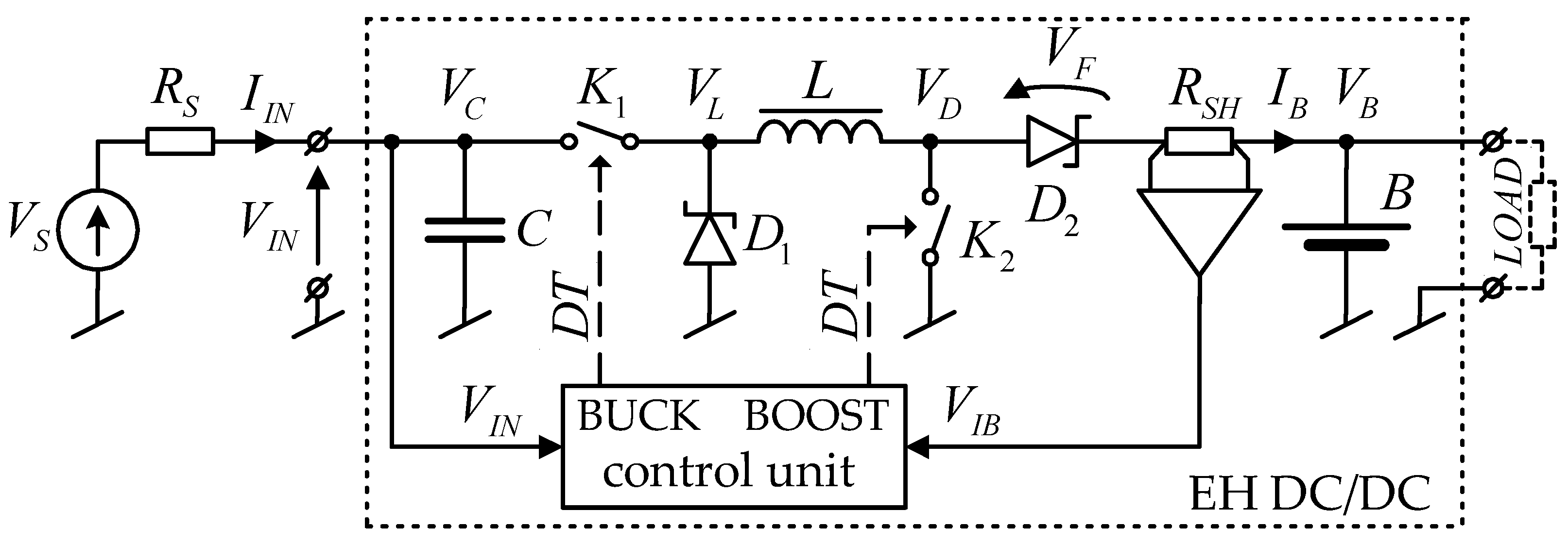
The voltage of the source may be lower or greater than the output voltage of the converter; therefore it is necessary to use a universal buck/boost converter, such as shown in Figure 3. The proposed converter can operate in three modes:
  • Boost mode in which voltage is converted up, switch K1 is turned ON, and K2 is switching;
  • Buck mode in which the voltage is converted down, switch K1 is switching, and K2 is turned OFF;
  • In a bypass mode when the output voltage is almost half the input voltage, switch K1 is turned ON and K2 is turned OFF.
To obtain near-optimal power at the converter’s output, it is necessary to develop an algorithm for controlling the converter’s keys K1 and K2. This algorithm must meet the following requirements:
  • Estimates the open-circuit voltage and output resistance of the source VS;
  • Select the appropriate operating mode of the converter (buck, boost, or bypass);
  • Selects the operating frequency of the converter and the duty factor of the control signal of the active switch in a given mode.
The operation of the converter in boost and buck mode must be analyzed to develop such an algorithm. This is a topic of the next sections.

3. Boost Mode Analysis

Before performing a detailed analysis, some general limitations affecting the device’s operation can be noted. Firstly, due to the source’s low available power, it is advantageous to operate in maximum power transfer mode; that is, the voltage across capacitor VIN should have an average value equal to half of the open-circuit voltage of the source VS and boost mode will be used if the required output voltage VB is greater than the input voltage VIN ≈ ½ VS.
Secondly, energy accumulation in capacitor C occurs exponentially, and therefore, due to the high resistance of the source, the duration of energy accumulation in capacitor C must be relatively long. However, it is advantageous to reduce this so that the voltage across the capacitor does not deviate significantly from ½ VS.
Thirdly, similarly, at the stage of energy transfer from capacitor C to coil L, the capacitor should not be discharged too much so that the voltage across the capacitor does not drop significantly below ½ VS. This means that this stage should be relatively short, and almost always, the device will operate with a discontinuous coil current.
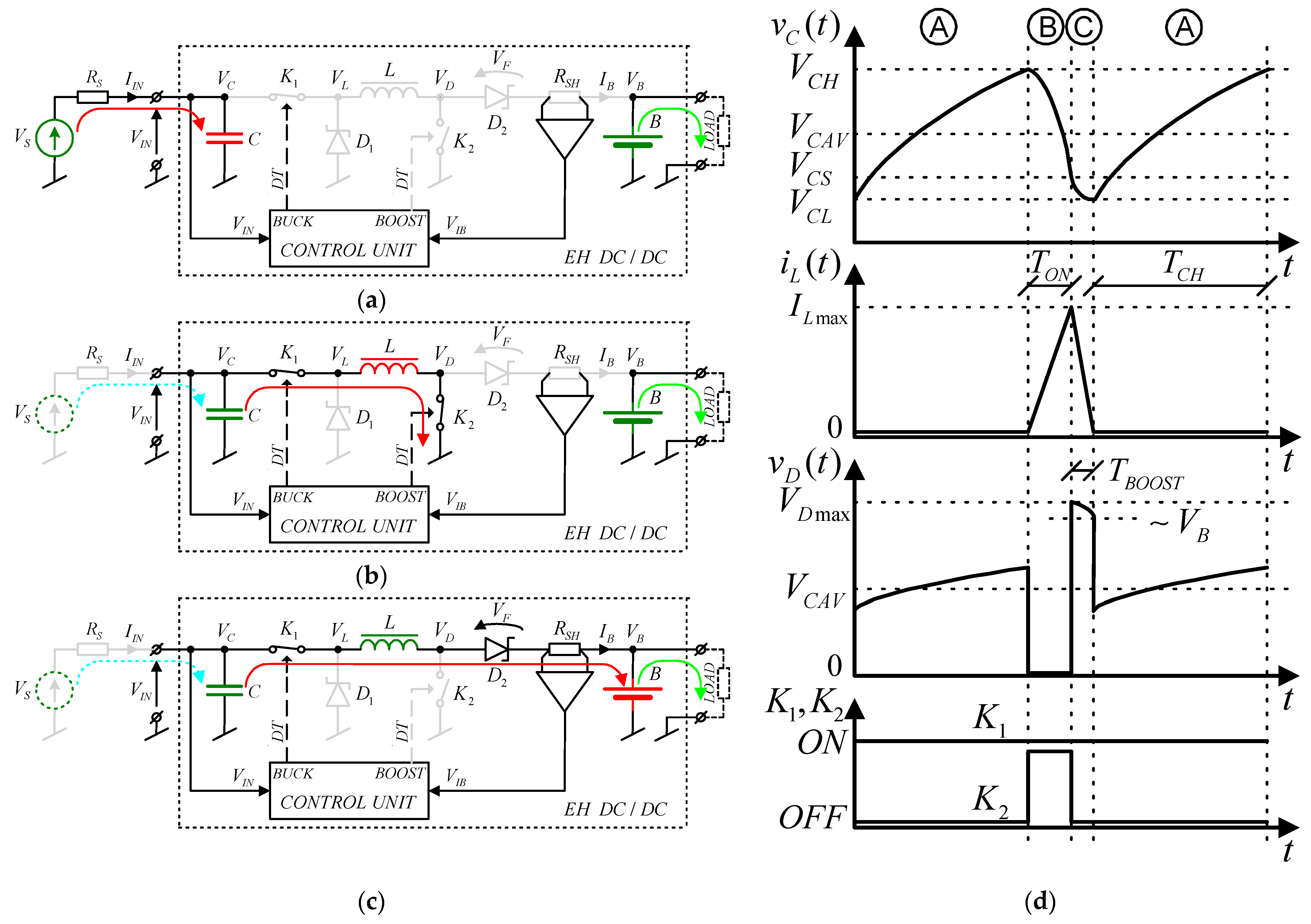
Based on those criteria, one boost cycle consists of three stages. The energy storage element and the primary energy flow of the stage are marked in red. The green colour indicates the output elements of the stage and the current drawn by the load. The dashed line in cyan indicates the current drawn from the source at stages other than A, as shown in Figure 4:
  • Stage A, when switch K2 is turned OFF, the capacitor is charging from the source, and the current of the coil L is zero;
  • Stage B, when switch K2 is turned ON and the energy is transferred from capacitor C to inductor L;
  • Stage C, when switch K2 is turned OFF, the capacitor is charging from the source, and the energy is transferred from coil L to load and battery B.
Bear in mind that switch K1 is always turned ON in boost mode.

3.1. Stage A: Energy Gathering in the Capacitor

3.1.1. Duration of Stage A

This is the longest of the three stages, in which the energy from the source is gathered in input capacitor C, the switch K2 is turned off, the diode D2 is reverse biased, and the inductor L current is equal to zero. As a result, the circuit could be simplified to an RC circuit, as shown in Figure 4a, where capacitor C is charging through resistor RS. To avoid a too-large voltage difference across the capacitor from the optimum value, ½ VS charging time should be a fraction of the RC circuit time constant:
T C H = k C H · R S · C ,
where kCH is a coefficient describing the duration of a stage with respect to system parameters of the converter and which should be significantly less than one. Coefficient kCH will be used to determine the frequency and the duty factor of the K2 switch control signal in the next section.

3.1.2. Input Voltage

At the end of this stage, the voltage across capacitor C reaches its maximum value:
V C H = V S V C L 1 e k C H · R S C R S C + V C L = V S 1 e k C H + V C L · e k C H .
This relationship will be used later.

3.2. Stage B: Transferring Energy from Capacitor to Inductor

3.2.1. Input Voltage and Duration of Stage B

In this stage, both switches, K1 and K2, are closed. Since the resistance RS is large, the circuit can be simplified to an underdamped LC circuit as ashown in Figure 4b. At the beginning of stage B, the capacitor C is charged. The voltage VC(t) reaches a maximum value VCH and further changes approximately according to the cosine function:
V C ( t ) = V C H · cos   2 π t T L C ,
where TLC is a period of the LC circuit oscillations equal to the following:
T L C = 2 π L C .
In order to avoid excessive lowering of voltage across the capacitor, the K2 switch can only be turned on for a time less than 1/4 of the natural oscillation period TLC. Therefore, it is convenient to express the turn-on time of the K2 switch using the parameter kON with respect to a quarter of the natural oscillation period:
T O N = k O N · T L C 4 = k O N · π 2 L C .
Parameter kON can take values from 0 to 1. Coefficient kON will be later used to determine the frequency and the duty factor of the K2 switch control signal.

3.2.2. Energy Balance

Energy taken from the capacitor during this stage is equal to the following:
Δ E C 1 = 1 2 C V C H 2 V C S 2 = 1 2 C · V C H 2 1 cos 2 k O N · π 2 = 1 2 C · V C H 2 sin 2 k O N · π 2 .
On the other hand, energy stored in the inductor is equal to the following:
Δ E L = 1 2 L · I L m a x 2 .
The energy extracted from the capacitor ΔEC1 is approximately equal to the energy stored in the inductor ΔEL. From (7), using (4), the maximum current of the coil can be determined, which is necessary for the proper selection of the coil L and the transistors K1 and K2:
I L m a x = C L · V C H sin k O N · π 2 = V C H L · T L C 2 π sin k O N · π 2 .

3.3. Stage C: Transferring Energy to the Battery

3.3.1. Input Voltage

At the time of turning the switch K2 OFF, the voltage on the capacitor is equal to the following:
V C S = V C H · cos k O N · π 2 .
The voltage decrease across the capacitor C in Stage C can be calculated, assuming a linear decrease of the coil current, using the following equation:
V C S V C L = 0 T b o o s t I L m a x C 1 t T b o o s t d t = I L m a x C · T b o o s t 2 .

3.3.2. Energy Balance

When the switch K2 is turned off, the voltage VD increases abruptly so that it ensures the continuity of the coil current iL(t). If the value of the inductance of the coil is large enough, the coil current decreases approximately linearly to zero. Thus, the energy stored in the coil is completely transferred to the battery B. At all times, energy is also drawn from capacitor C:
Δ E C 2 = 1 2 C V C S 2 V C L 2 ,
And the total energy extracted from the capacitor during one full cycle is equal to:
Δ E C = Δ E C 1 + Δ E C 2 = 1 2 C V C H 2 V C L 2 .
On the other hand, the energy delivered to the battery and load can be calculated based on the charge transferred to the output:
Q L O A D = 1 2 I L m a x · T b o o s t ,
where Tboost is the duration of stage C. Finally, the energy ELOAD delivered to the battery and the load is equal to the following:
E L O A D = Q L O A D · V D m a x = 1 2 I L m a x · T b o o s t · V D m a x ,
where VDmax is almost constant voltage in stage C equal to battery voltage plus diode D2 forward voltage drop.
It can be assumed that the total energy taken from the capacitor ΔEC and the energy transferred to the load calculated from the charge ELOAD are equal to each other:
1 2 C V C H 2 V C L 2 = 1 2 I L m a x · T b o o s t · V D m a x .
It is true that the capacitor C is charged from the source constantly, but the large resistance of the source means that this is of little importance for the energy balance.

3.3.3. Duration of Stage C

Time Tboost can be calculated by transforming (15):
T b o o s t = C I L m a x · V C H 2 V C L 2 V D m a x .
Formula (16), after substitution (8) and then using (4), takes the form of the following:
T b o o s t = C · L T L C 2 π sin k O N · π 2 · V C H 2 V C L 2 V C H · V D m a x = T L C 2 π · V C H 2 V C L 2 V C H · V D m a x sin k O N · π 2 .
This formula will be simplified in the next subsection to Equation (29) and will be used in the control algorithm.
Stage C ends when the coil current drops to zero, that is when all the energy stored in the coil is transferred to the load and battery B. The voltage on the capacitor C then has its minimum value of VCL.

3.4. Determination of the Operating Frequency and the Duty Factor in Boost Mode

The purpose of this subsection is to derive formulas describing the coefficients kON and kCH to implement the converter control algorithm in boost mode. As in a classic converter, the quantities used to calculate these coefficients are the input and output voltage of the converter. The former is the open-circuit voltage VS and can be easily measured by the control unit. The latter is voltage VDmax, which is roughly known as it is equal to battery voltage plus diode D2 forward voltage drop.
As mentioned earlier, the converter should work in near maximum power transfer mode, which means that input voltage VIN (i.e., the voltage across capacitor C VC) should have a value close to ½ VS. Therefore, it is convenient to use the average value VCAV of the voltage on capacitor C, which is defined as follows:
V C A V V C H + V C L 2 = V S 1 e k C H + V C L 1 + e k C H 2 ,
where (2) was used to substitute VCH.
Although VCAV should be equal to ½VS, due to the simulation and verification studies, let us assume first that VCAV can take any values and derive analytical relations for VCL and VCH. The former could be obtained after a simple transformation of (18):
V C L = 2 1 + e k C H V C A V 1 e k C H 1 + e k C H V S ,
and the latter by substituting (19) to (2):
V C H = 2 e k C H 1 + e k C H V C A V + 1 e k C H 1 + e k C H V S .
Let’s return to the energy balance described by Equation (15), but this time dispose of the ILmax and Tboost. Using Equations (9) and (10), the following equation can be written:
I L m a x · T b o o s t = 2 C V C H cos   k O N · π 2 V C L ,
and after substituting it into the Equation (15), one gets the following:
1 2 V C H 2 V C L 2 = V C H cos   k O N · π 2 V C L · V D m a x .
This formula can be transformed, using the definition of VCAV (18), to determine kON:
cos   k O N · π 2 = 1 2 V C H 2 V C S 2 V C H · V D m a x + V C L V C H = V C H + V C L 2 V C H V C L V C H · V D m a x + V C L V C H = V C A V V D m a x 1 V C L V C H + V C L V C H ,
where the ratio of VCL and VCH can be calculated using (19) and (20) as follows:
V C L V C H = 2 V C A V 1 e k C H V S 2 V C A V · e k C H + 1 e k C H V S .
After taking into account that the average voltage across capacitor VCAV should be equal to half of the voltage VS, Equation (24) simplifies to the following:
V C L V C H = V S 1 e k C H V S V S · e k C H + 1 e k C H V S = e k C H .
Substituting (25) into (23):
cos   k O N · π 2 = 1 2 V S V D m a x 1 e k C H + e k C H .
which finally leads to the following:
k O N = 2 π a r c c o s 1 2 V S V D m a x 1 e k C H + e k C H ,
and:
k C H = l n V Dmax cos   k O N · π 2 1 2 V S V D m a x 1 2 V S .
Equations (27) and (28) tie together two basic control parameters, kON and kCH and are essential for the controlling algorithm of the converter in boost mode. Admittedly, they do not allow the determination of both control parameters independently, but by knowing or choosing one of the parameters, the value of the other can be calculated.
The actual values of the source resistance RS, inductance L, and capacitance C are required to convert the dimensionless kON and kCH coefficients into TON and TOFF times for the K2 switch. The determination of Rs and the selection of L and C will be presented in the next section. For the following derivation, let’s assume that these values are known.
(5) directly gives the value of TON. Calculating TOFF is more convoluted because TOFF time is the sum of Tboost and TCH, and expression (17) for Tboost depends on VCH and VCL. Using the definition of VCAV, the Equation (17) becomes the following:
T b o o s t = T L C π · V C H + V C L 2 V C H V C L V C H · V D m a x sin k O N · π 2 = T L C π · V C A V V D m a x sin k O N · π 2 · V C H V C L V C H ,
Now let’s simplify it by assuming that the average voltage on the capacitor VCAV has a value equal to half of VS and by using Equation (25):
T b o o s t = T L C 2 π · V S V D m a x sin k O N · π 2 1 e k C H .
Since the duration times of each stage are already known, both the frequency and the duty factor of the converter’s control signal can be calculated from the following definitions:
f 1 T O N + T b o o s t + T C H .
d T O N T O N + T b o o s t + T C H .

4. Buck Mode Analysis

Notably, all three comments about boost mode, mentioned in Section 3, are also true for buck mode. Firstly, the converter ought to operate in maximum power transferring mode, which means that the voltage across the capacitor VIN should have an average value equal to half the open-circuit voltage of the source VS. Secondly, the time of energy accumulation in the capacitor C from the source must be relatively long, but not too long to avoid too much increase of the voltage across the capacitor in relation to the desired value of ½ VS. Thirdly, the duration of energy transfer from the capacitor C to the coil L should be short so that the voltage across the capacitor does not decrease significantly from ½ VS.
The main difference between buck and boost mode is the lack of a separate coil discharge stage. In buck mode, the energy stored in the coil is transferred to the load at the beginning of stage A, simultaneously with the charging of the capacitor from the source, which means that almost always the device will operate with a discontinuous coil current.
Therefore, one buck cycle consists of only two stages as shown in Figure 5:
  • Stage A, when switch K1 is turned OFF, the capacitor is charging from the source, and at the beginning, the energy is transferred from coil L to load and battery B, and in the second part of this stage the current of coil L is zero;
  • Stage B, when switch K1 is turned ON and the energy is transferred from capacitor C to inductor L.
  • Buck mode will be used if output voltage VB is significantly lower than input voltage VIN ≈ ½ VS. Noting that switch K2 is always turned OFF in boost mode.

4.1. Stage A: Energy Gathering in the Capacitor

In this phase, the K1 switch is opened, and as in phase A of boost mode, the input capacitor is separated from the output circuit. As a result, the input voltage waveform is identical to that in phase A of boost mode, and relations (1) and (2) apply equally to stage A of buck mode.

4.2. Stage B: Transferring Energy to Inductor and Battery

During stage B the switch K1 is closed. As in stage B of boost mode, the circuit can be simplified to an underdamped LC circuit in series with a battery B (Figure 5b). At the beginning of stage B, the capacitor C is charged, the voltage VC(t) reaches a maximum value VCH, and further changes according to the cosine function:
V C ( t ) = V C H V D m a x · cos   2 π t T L C + V D m a x .
At the end of this stage, the voltage across capacitor C reaches its minimum value:
V C L = V C H V D m a x · cos   k O N · π 2 + V D m a x .
The above relationships are true, assuming that VCL is greater than VDmax, which should always be true if the converter is in buck mode.
It is still necessary to determine the maximum current of the coil because of its importance while selecting both the coil L and transistor K1. It can be calculated by considering how the current of the coil is changing during stage B. Using (33), one gets the following:
I L m a x = 1 L 0 T O N V C ( t ) V D m a x d t = 1 L 0 T O N V C H V D m a x · cos   2 π t T L C d t = T L C 2 π · V C H V D m a x L sin k O N · π 2 .

4.3. Determination of the Operating Frequency and the Duty Factor in Boost Mode

As for boost mode, let’s derive formulas for calculating the coefficients kON and kCH based on open-circuit voltage VS and the voltage VDmax, which is equal to battery voltage plus diode D2 forward voltage drop.
Using Formulas (2), (18) and (34), one can write a system of three equations with 4 unknowns: VCH, VCL, kON, and kCH:
V C H = V S 1 e k C H + V C L · e k C H V C L = V C H V D m a x · cos   k O N · π 2 + V D m a x V C A V = V C H + V C L 2 .
from which VCH should be eliminated as follows:
2 V C A V V C L = V S 1 e k C H + V C L · e k C H V C L = 2 V C A V V C L V D m a x · cos   k O N · π 2 + V D m a x ,
and, in the next step, VCL should be eliminated too, as follows:
V C L 1 + e k C H = 2 V C A V V S 1 e k C H V C L 1 + cos   k O N · π 2 = 2 V C A V V D m a x · cos   k O N · π 2 + V D m a x ,
1 + e k C H 1 + cos   k O N · π 2 = 2 V C A V V S 1 e k C H 2 V C A V V D m a x · cos   k O N · π 2 + V D m a x .
Yet again, after taking into account that the average voltage across capacitor VCAV should be equal to ½VS, Equation (39) simplifies to the following:
1 + e k C H 1 + cos   k O N · π 2 = V S e k C H V S V D m a x · cos   k O N · π 2 + V D m a x .
And finally, one gets the following:
k O N = 2 π a r c c o s 1 + e k C H · V D m a x V S e k C H 1 + e k C H · V D m a x V S ,
or the following:
k C H = l n V S cos   k O N · π 2 + V Dmax 1 cos   k O N · π 2 V S V Dmax 1 cos   k O N · π 2 .
As for boost mode, let’s assume that the values of the source resistance Rs, inductance L, and capacitance C are known. Then, (5) gives the value TON, and (1) TOFF. In buck mode, the frequency and the duty factor of the converter’s control signal can be calculated from the following definitions:
f 1 T O N + T C H .
d T O N T O N + T C H .

5. Design Recommendations—How to Choose L and C

First, let’s note that before designing a converter, it is necessary to know roughly the range of variation of the source resistance and open-circuit voltage because these parameters strongly affect the selection of the components.
From the formulas presented so far, it could be unclear what the values of inductance L and capacitance C should be, and, in general, it is impossible to derive formulas to calculate these values. Nevertheless, it is possible to show some restrictions on them.
The device is supposed to measure the source resistance and open-circuit voltage periodically by opening switch K1 and waiting a sufficiently long time until the voltage on capacitor C is almost in a steady state. Such a measurement should take significantly less time compared to the rate of change of both measured quantities. It means that the time constant of the input circuit, consisting of source resistance and input capacitor RS·C, should not be too long. This leads to a restriction on the capacitance C:
C M A X T M _ m i n R S _ m a x ,
where RS_max is the expected maximum value of source resistance and TM_min is the minimum time between measurements of source parameters. Both values need to be measured or evaluated experimentally. In the case of the stray current energy harvester, the rate of change of open-circuit voltage is usually less than 10 V/s and the source resistance usually changes much more slowly than 1 Ω/s.
On the other hand, capacitance C cannot be too small because either the peak-to-peak value of the voltage ripple across the capacitor C would be too large, or the operating frequency of the converter would be too high. The peak-to-peak ripple voltage VCpp can be calculated using Formulas (19) and (20), which are true for both boost and buck modes, assuming that the average voltage VCAV is equal to half the open-circuit voltage VS:
V C p p = V C H V C L = 2 e k C H 2 1 + e k C H V C A V 2 · 1 e k C H 1 + e k C H V S = 1 e k C H 1 + e k C H V S .
From Equation (46), constraints on the maximum value of kCH can be derived as follows:
k C H _ m a x = l n 1 V C p p V S 1 + V C p p V S ,
where VCpp/VS is the assumed maximum value of the ratio of ripple to the open-circuit voltage. Since kCH must be less than 1, it limits the maximum ratio of VCpp/VS to 0.462. Usually, VCpp/VS << 1.
The working frequency of the converter depends primarily on the duration of stage A, so it can be approximated as follows:
f 1 k C H · R S · C   .
Finally, the formula for the minimum value of capacitor C can be derived as follows:
C M I N > 1 k C H _ m a x · f m a x · R S _ m a x   ,
where fmax is the maximum acceptable operating frequency of the converter.
As for the selection of the inductance of the coil, it should be noted that the inductance ought not to be too small, so that the maximum coil current is not too large, but at the same time, the inductance should be small enough so that in stage B the circuit can be simplified to an underdamped RLC circuit. For the latter condition to be met, the following relationship must be satisfied:
L M A X 4 · R S _ m i n 2 · C   ,
where the definition of damping factor ζ of the parallel RLC circuit was used and RS_min is the minimal expected value of source resistance.
Comparing relations (8) and (35), one can expect a higher maximum coil current in boost mode. Substituting (20) into (8) and assuming that VCAV is equal to half of VS leads to the following:
I L m a x = C L · 1 1 + e k C H V S · sin k O N · π 2 ,
from which the minimum value of inductance L can be calculated as follows:
L M I N > 1 1 + e k C H V S _ m a x 2 · C I L m a x 2 · sin 2 k O N · π 2 .
Substituting the Formula (27) and using trigonometric identity for sin (arccos(x)) one gets the following:
L M I N > 1 1 + e k C H V S 2 · C I M A X 2 · 1 1 2 V S V D m a x 1 e k C H + e k C H 2 ,
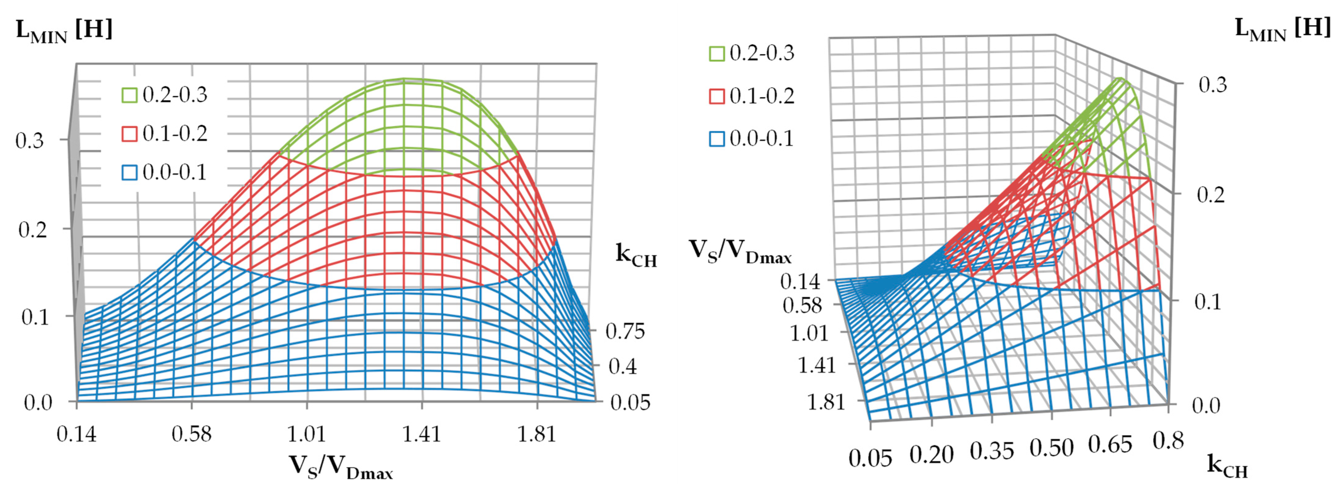
where IMAX is the maximum acceptable coil L current value and is the design parameter. Unfortunately, both coefficient kCH and the open-circuit voltage VS vary over wide ranges and the equation is relatively complicated. Therefore, it is very useful to know how the minimum value of the inductor depends on coefficient kCH and the open-circuit voltage VS changes (Figure 6). The influence of coefficient kCH is almost linear, and the influence of the open-circuit voltage looks a bit like a distorted parabola. Hence, the Formula (53) can be roughly approximated as follows:
L M I N > k C H _ m a x π · C I M A X 2 · V D m a x 2 ,
where kCH_max is the maximum value of coefficient kCH to be used.
In summary, Formulas (45) and (49) describe the limitations on the value of capacitor C, while Formulas (50) and (54) restrict the value of the coil L. Since there are no other restrictions on values C and L arising from the analytical model, the designer should choose values of these elements considering other factors, such as dimensions, price, and availability. It should be emphasized that, as it is shown in Section 7, even the influence of exact values of these elements on converter parameters is not critical.

Example of Choosing the Capacitor C and the Coil L

Suppose that the unconventional energy source has the following properties:
  • the open-circuit voltage of the source VS is less than 40 V and changes with slew rate SRS of less than 10 V/s;
  • a minimum usable open-circuit voltage VSmin of 2 V;
  • source resistance from RS_min = 50 Ω to RS_max = 200 Ω and rate of change much slower than 1 Ω/s.
  • The requirements for a converter are as follows:
  • an output voltage VB of 12.8 V;
  • the voltage drop across the diode VF of 1.0 V;
  • a maximum coil current ILmax of 3 A;
  • a maximum ratio of amplitude VCpp to open-circuit voltage VS of 10%;
  • operating frequency f less than 4 kHz.
Assuming that the maximum acceptable mismatch between the used in the calculation and the actual value of open-circuit voltage ΔVS should be less than 1 V the time between measurements of source parameters tM_min can be calculated using tM = ΔVS/SRS and is equal to 100 ms.
From (45) one can calculate that the maximum value of capacitor CMAX should be much smaller than 500 µF, from (47) the maximum value of kCH is equal to 0.2, and from (49) the minimum value of capacitor CMIN equal to 6.25 µF.
Let us assume it was decided to use 4 parallel connected 10 µF MLCC capacitors and the capacitance C is equal to 40 µF.
Using (50) one can obtain the maximum value of coil inductance LMAX equal to 0.4 H and using (54) the minimum value of coil LMIN equal to 55 µH. Selecting a coil with an inductance of 100 µH satisfies these limitations.

6. Control Algorithm

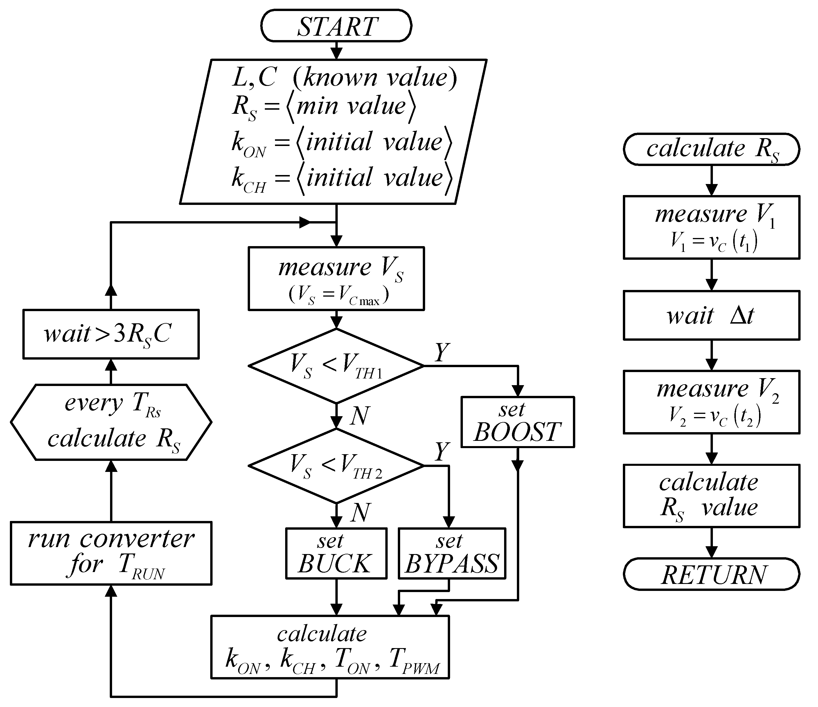
As mentioned in Section 2, the control algorithm must estimate the open-circuit voltage and output resistance of the source VS, choose the converter’s operating mode, and determine the operating frequency and the duty factor of the converter control signal. The control algorithm is shown in Figure 7.

6.1. Measuring the Power Source Parameters

It is easy to see that to measure the open-circuit voltage VS, one needs to simply open the K1 switch and wait until the voltage across the capacitor is in a steady state. However, you can simultaneously measure the output resistance of the source RS. The voltage across the capacitor changes in the buck mode after opening switch K1 and in the boost mode Tboost after opening switch K2 as follows:
V C t = V S V 1 1 e t R S C + V 2 ,
where V1 is the measured value of the voltage across the capacitor after opening switch K1 in buck mode or after Tboost after opening switch K2 in the boost mode. After time Δt, the voltage V2 across the capacitor should be measured again. If the values V1, V2, and Δt are known, (55) can be transformed to calculate source resistance RS:
R S = t C · l n V S V 2 V S V 1 .

6.2. Choosing the Operating Mode

The operating mode is selected on the basis of the ratio of the open-circuit voltage VS to the VDmax voltage. The voltage VDmax is known, it depends primarily on the type of battery used in the device (and configuration of batteries if there are more than one), and the open-circuit voltage VS must be measured.
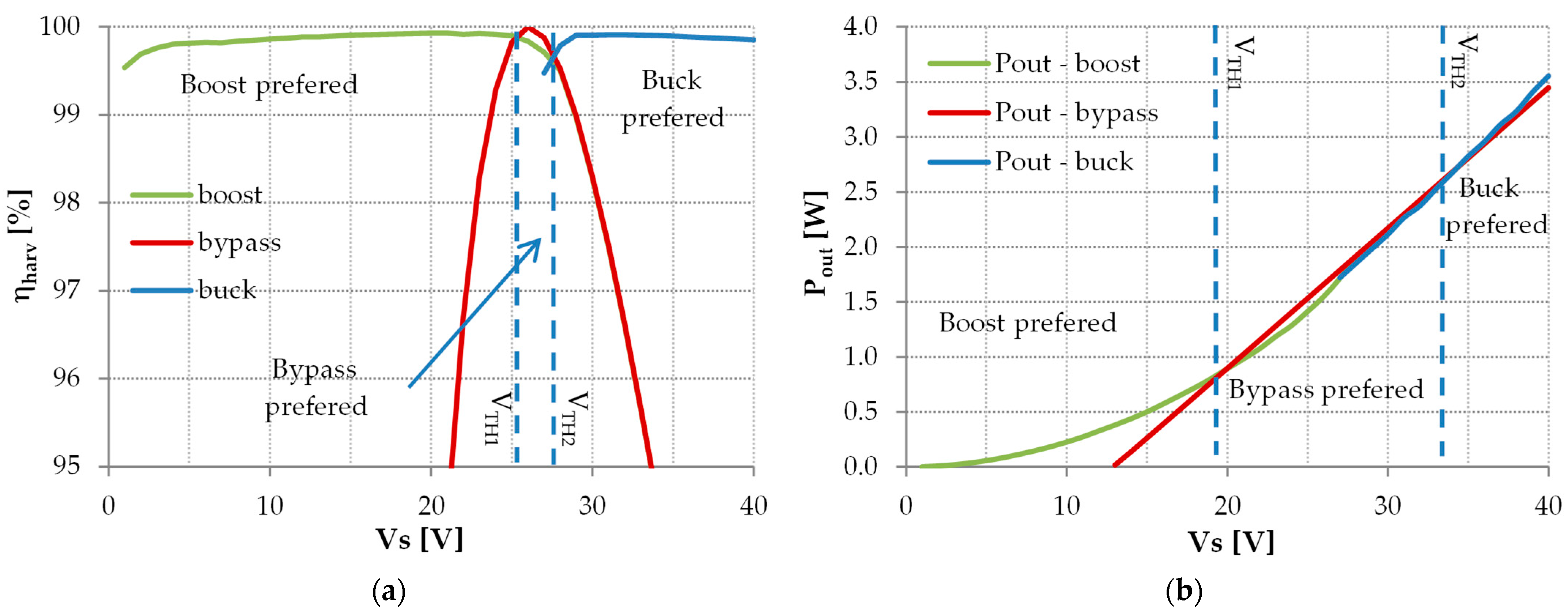
If half of the open-circuit voltage VS is less than VDmax, use boost mode. On the other hand, if half of the open-circuit voltage VS is significantly greater than VDmax, the buck mode should be used. If half of the open-circuit voltage VS is slightly larger than VDmax, it is advantageous to use the bypass mode. The limits of the use of different modes, shown in Figure 8, are not precisely defined, as they are not critical for the performance of the converter.

6.3. Determining Frequency and Duty Factor of the Control Signal

In the bypass mode, the switch K1 is permanently closed and the switch K2 is permanently opened.
In contrast, in the boost mode, the switch K1 is permanently closed, and the transistor K2 is switching. The buck mode is similar, but in this case, the transistor K1 is switching, while switch K2 is permanently opened. To calculate the frequency and duty factor of the control signal of the switching transistor, first, choose a reasonable value of coefficient kCH or kON and then calculate, using Formula (27) or (28) respectively, the second coefficient. As explained earlier, both coefficients should be less than 1, and Formula (47) limits the maximum value of the coefficient kCH.
Next, it is necessary to calculate TCH, TON, and forboost mode Tboost, using Formulas (1), (5) and (30), respectively. Finally, the frequency and duty factor of the control signal can be determined using (31) and (32) for boost mode and (43) and (44) for buck mode.
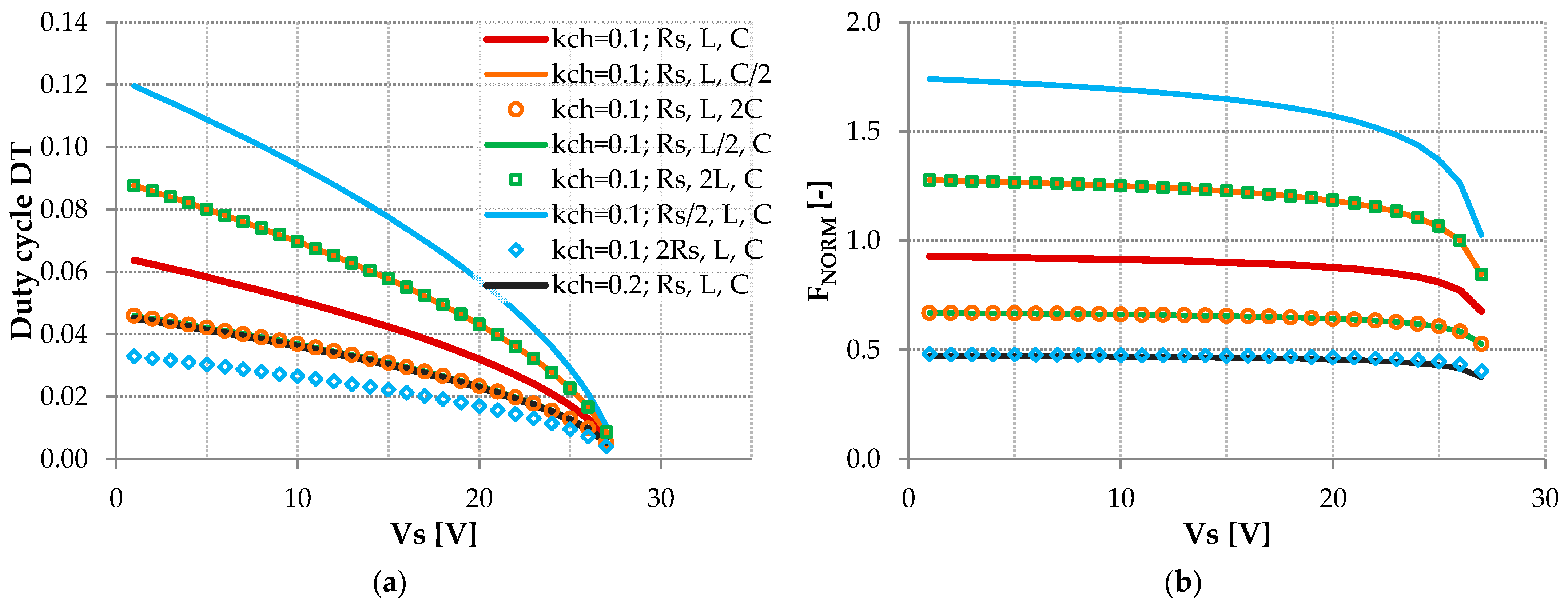
In summary, there are two ways to determine the parameters of the control signal. One is to select kON and then calculate kCH using (28). The other is to select kCH and then calculate kON using (27). In both cases the frequency and duty factor can be calculated using Formulas (1), (5), (30), (31) and (32). Figure 9 and Figure 10 show how these parameters depend on open-circuit voltage VS, different values of capacitance C and inductance L, and different effective input resistances for boost mode.
To facilitate the selection of a “reasonable” kCH or kON factor initially, it is useful to know the effect of these parameters on the converter’s energy harvesting efficacy. Firstly, however, it is necessary to calculate the power supplied to battery B; the load; and define this efficacy.
The mean power that is extracted from the capacitor can be calculated by substituting (19) and (20) into (12). After simplification, one obtains the following:
P C = 1 2 C T P W M V C H 2 V C L 2 = 2 C T P W M · 1 e k C H 1 + e k C H V S V C A V · V C A V
where TPWM is the duration time of one full cycle of the converter. However, in boost mode, the power delivered to the battery and load is, at the same time, greater due to the current Iin flowing from the source in Stages B and C:
P a d d = I i n · V C A V T O N + T b o o s t T P W M = V S V C A V R S · V C A V T O N + T b o o s t T P W M
and is reduced by the power lost in diode D2:
P d = 1 2 I L m a x · V F T b o o s t T P W M ,
where VF is the diode D2 forward voltage drop. The final formula for the power supplied to the battery B and the load can be written as follows:
P O U T = P C + P a d d P d .
On the other hand, according to maximum power transfer theorem, the power available from the source is equal to the following:
P S A v a i l = V S 2 4 R S .
Now it is time to define the energy conversion efficiency factor ηconv:
η c o n v P O U T P S A v a i l · 100 % .
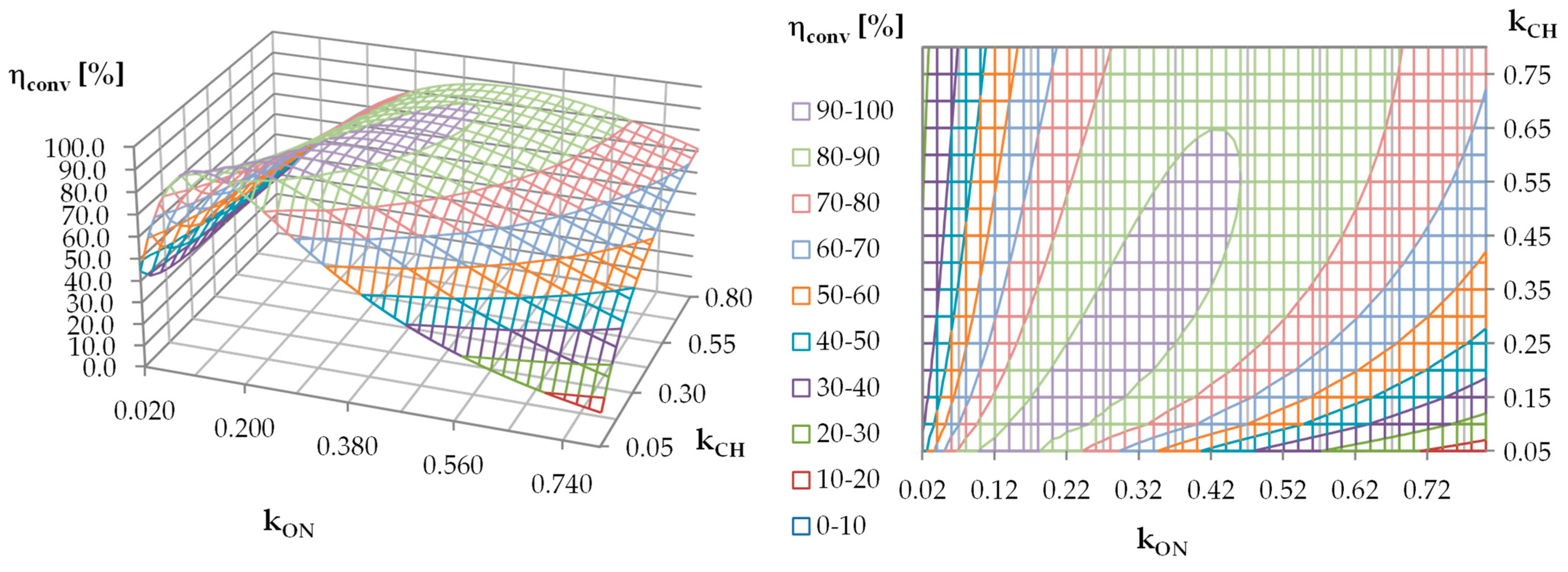
Figure 11 shows how the energy conversion efficiency factor ηconv depends on coefficients kCH and kON.
Finally, let us define harvesting efficacy factor ηharv:
η h a r v P I N P S A v a i l · 100 % ,
where PIN is the power delivered by the source to the converter and can be calculated as follows:
P S o u t = I I N · V I N V S V C A V R S · V C A V .
Energy harvesting efficacy is actually a measure of the matching of the input resistance of the converter to the source resistance and reaches a maximum value of 100% in the case of perfect matching. Figure 12 shows that the energy harvesting efficacy factor ηharv is not very sensitive to the coefficients kCH and kON.

7. Simulations of the Proposed Converter and Verification of the Derived Formulas

The LT-Spice program was used to verify the design presented in previous sections. The method of simulating the boost operation is presented in Figure 13. For the buck mode, the circuit was the same; simulations differed only in the directives of the control signals.
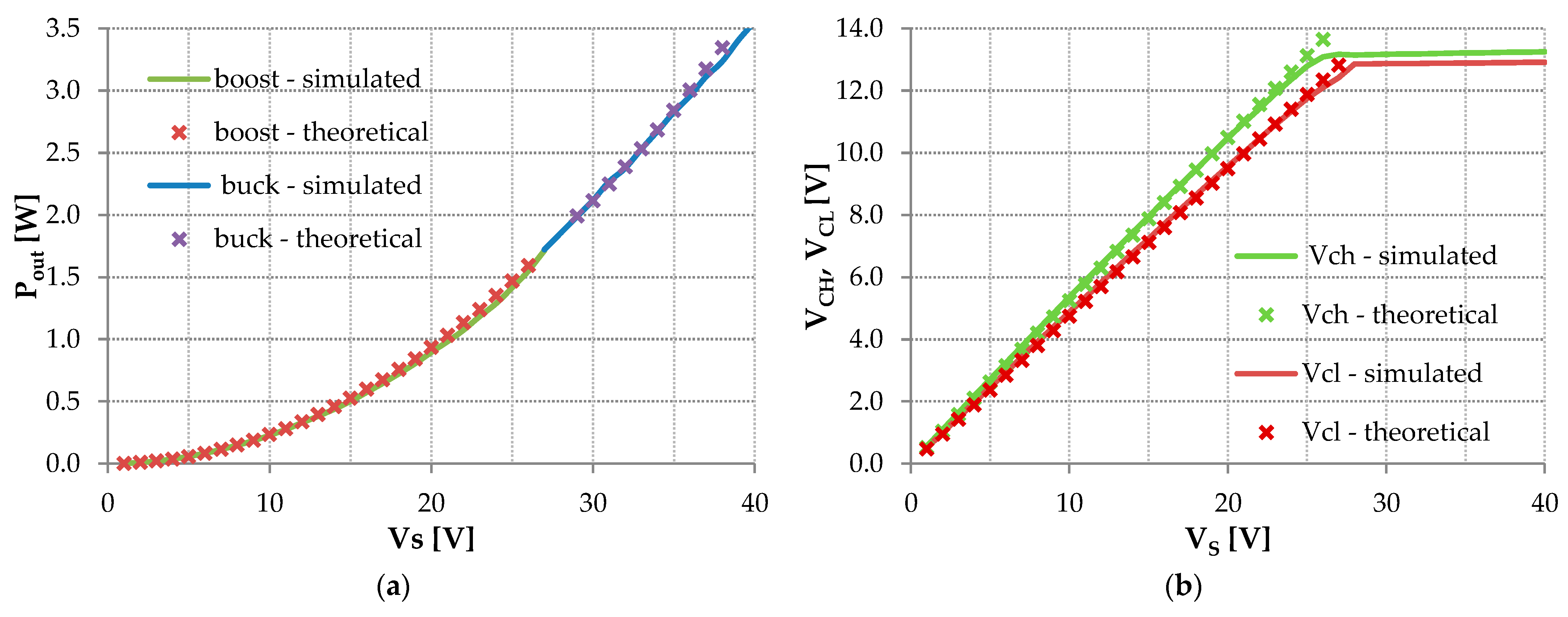
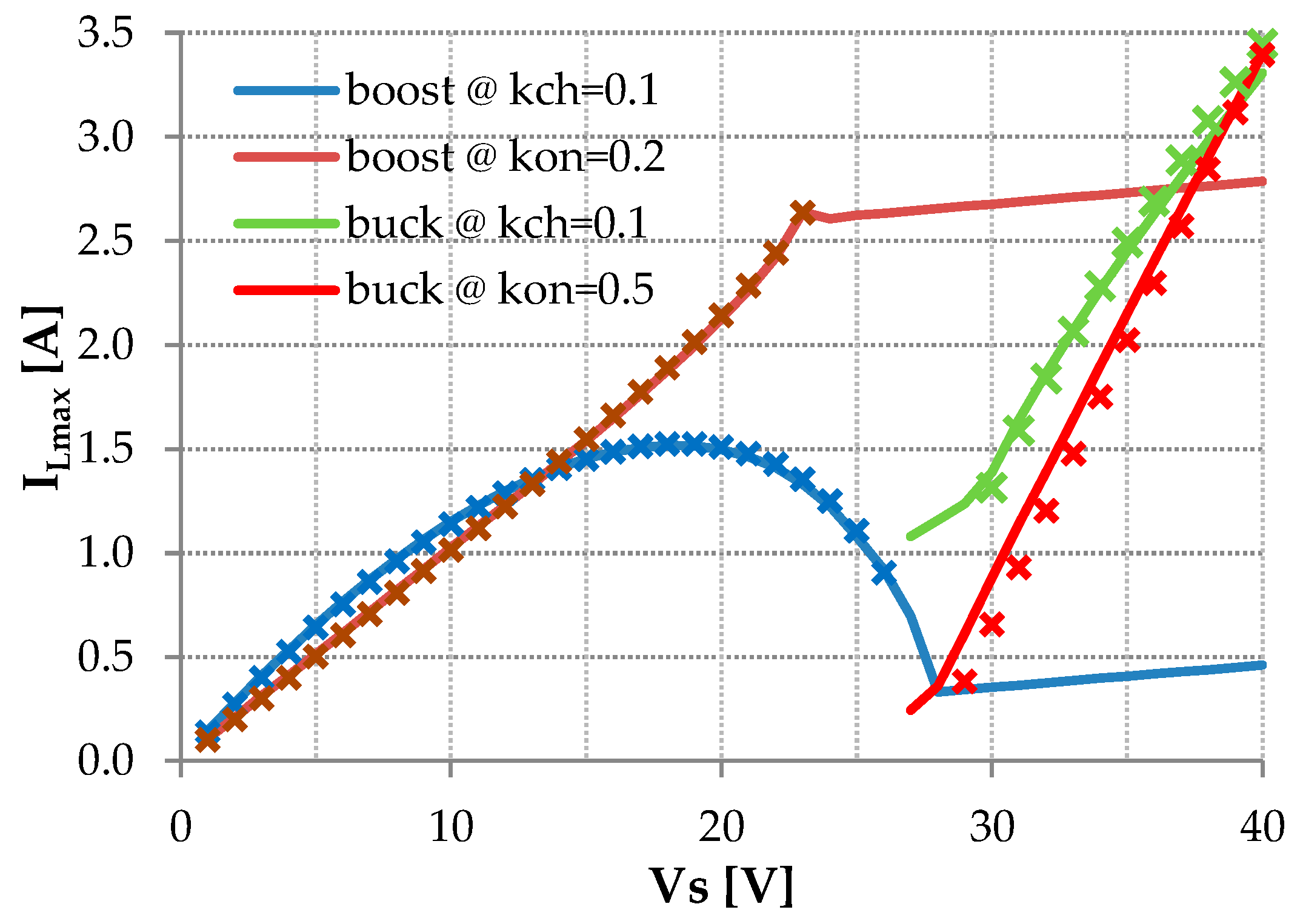
Figure 14 and Figure 15 show very good agreement between simulation results and corresponding analytical solutions for exemplary quantities: output power, minimum and maximum voltage across the capacitor in one converter cycle, and maximum coil current. These quantities were chosen because of their relevance to the characterization of the converter.
Simulations were also used to determine the impact of component tolerances on converter operation and the effect of inaccuracy in determining the source resistance on how the converter works. Figure 16 shows that the effect of capacitance C variability is the smallest. The influence of the remaining quantities is slightly larger but still not critical.

8. Hardware Implementation

The proposed algorithm was implemented in a prototype of the energy harvesting device, which consists of a Nucleo development board with an STM32L152 microcontroller and a prototype universal buck–boost converter designed by the authors of this article. The test bench consisted of an IT6721 power supply, Sanwa PC5001a multimeters, Siglent SDS1104X-E oscilloscope, a decade resistor, and a standard 12 V 7 Ah gel battery. To experimentally verify the concept a slightly modified previously designed device was used. This means that the prototype was not fully optimized, but it is not the subject of this article.

8.1. Static Measurements Without Disturbance

The power supply was used as an energy source and allowed to set the voltage VS from 0 V to 60 V. Due to the very low output resistance of the power supply, a decade resistor was used to set the output resistance of the emulated energy source RS to the desired value Figure 17 and Figure 18. During the static tests, the decade resistor was set to 100 Ω.
The actual waveforms for boost and buck modes of input voltage (voltage across capacitor C), the current of the coil L, and voltage VD at the anode of diode D2 are in perfect agreement with those predicted and modeled in the previous section (Figure 4d and Figure 5c).
All three stages of boost mode are clearly visible in Figure 19, which presents waveforms of the converter working in boost mode:
  • Charging of the capacitor from the source (stage A), when switch K2 is turned OFF (yellow trace is low) and the current of the coil L is zero (cyan trace is zero);
  • energy transfer from capacitor C to inductor L (stage B), when switch K2 is turned ON (yellow trace is high) and the coil’s current increases linearly (ramp up of cyan trace);
  • energy transfer from coil L to load and battery B (stage C), when switch K2 is turned OFF (yellow trace is low), the coil’s current decreases linearly (ramp down of cyan trace), and the diode D2 is still biased forward (green trace is high).
It should be emphasized that the assumption of an almost linear rise (in stage B) and then fall (in stage C) of the coil current was confirmed during the measurements of the prototype, as can be seen in Figure 19.
Also, both stages of buck mode are clearly visible in Figure 20, which presents waveforms of the converter working in buck mode:
  • charging of the capacitor from the source (stage A), when switch K1 is turned OFF (yellow trace is low) and the current of the coil L fast and linearly drops to zero at the beginning of the stage and then is zero until the end of the stage (cyan trace);
  • energy transfer from capacitor C to inductor L (stage B), when switch K1 is turned ON (yellow trace is high) and the coil’s current increases (cyan trace).
  • It should be emphasized that the assumption of an almost linear fall in stage B of the coil current was confirmed during the measurements of the prototype (Figure 20).
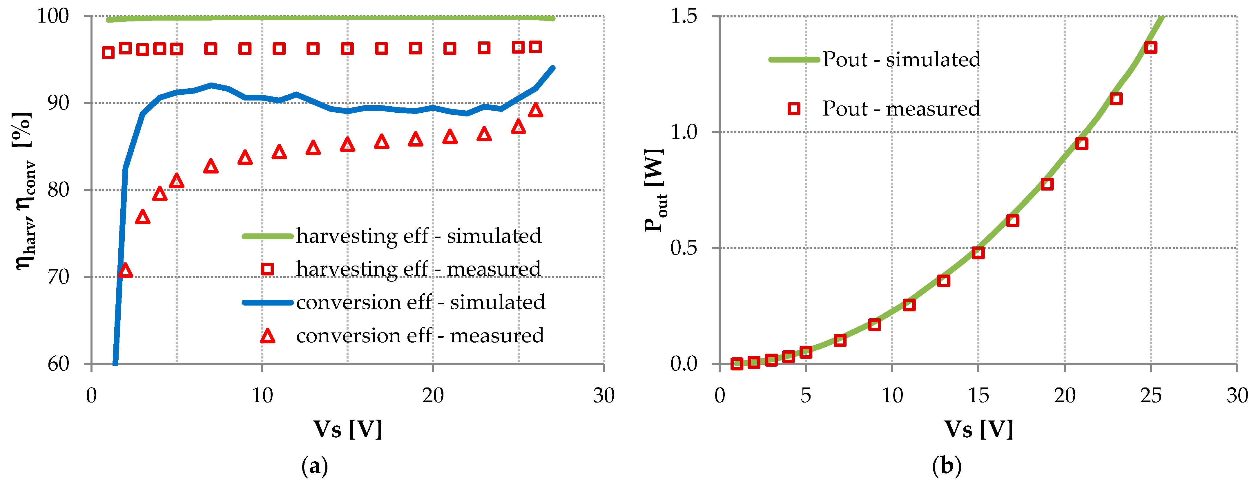
The results of the comparison between simulations and experimental results are presented in Figure 21, Figure 22 and Figure 23. The harvesting efficacy factor ηharv is a few percent lower than the values resulting from the simulations, which is mainly due to the fact that the device is powered from the battery, making the output current systematically lower than simulated. Less influential are power losses in the device not taken into account in the simulations, e.g., on the resistance of tracks, wires, and contacts, on the series resistance of capacitors. The energy conversion efficiency factor ηconv for open-circuit voltage VS > 15 V is in perfect match with simulation results, but lower values of VS tend to be lower than simulated results, as can be seen in Figure 21a. Again, this can be perfectly explained by the fact that the device is powered by the battery. Since the power taken from the battery by the device is approximately constant, the higher the power given off by the converter (which is the case for higher VS voltages) the smaller the difference between measurements and simulations. The output power over the entire range of open-circuit voltage VS variations agrees with the simulations (Figure 21b).
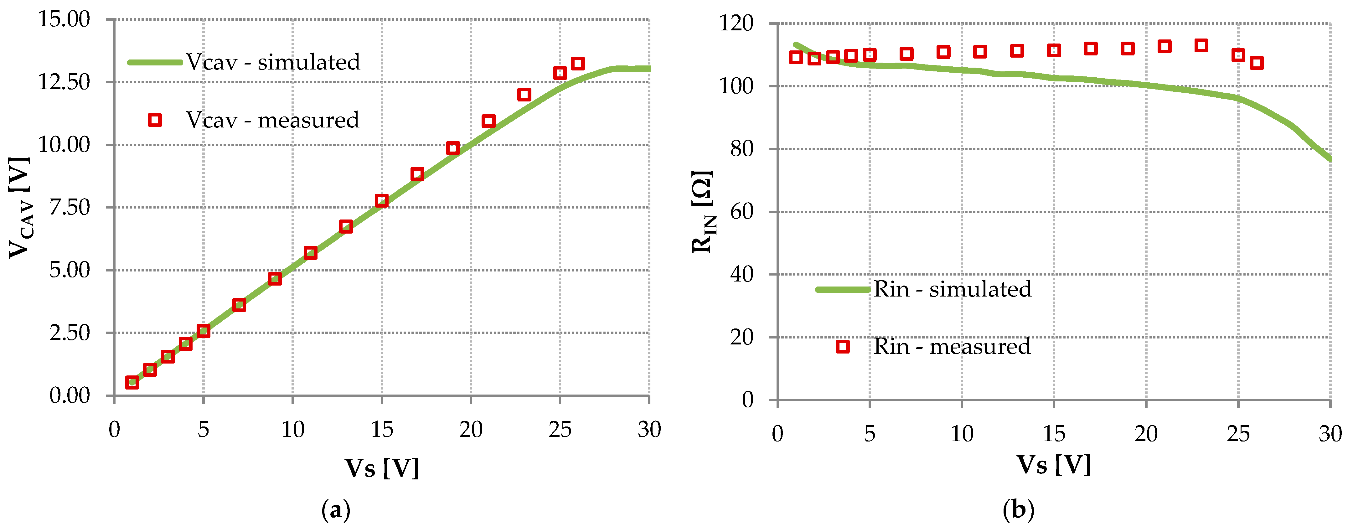
Figure 22 shows how well input resistance matches to source resistance: if the converter operates in maximum power transfer mode, the input voltage should be equal to half of the open-circuit voltage, and the input resistance should be equal to the source resistance. Both the average voltage across input capacitor C and input resistance are slightly higher than the simulation results for higher values of VS, as can be seen in Figure 22. However, overall, the match to source resistance is very good; in the worst case, the input resistance differs from source resistance by less than 13%, which means that only 0.4% of available power is lost due to resistance mismatch.
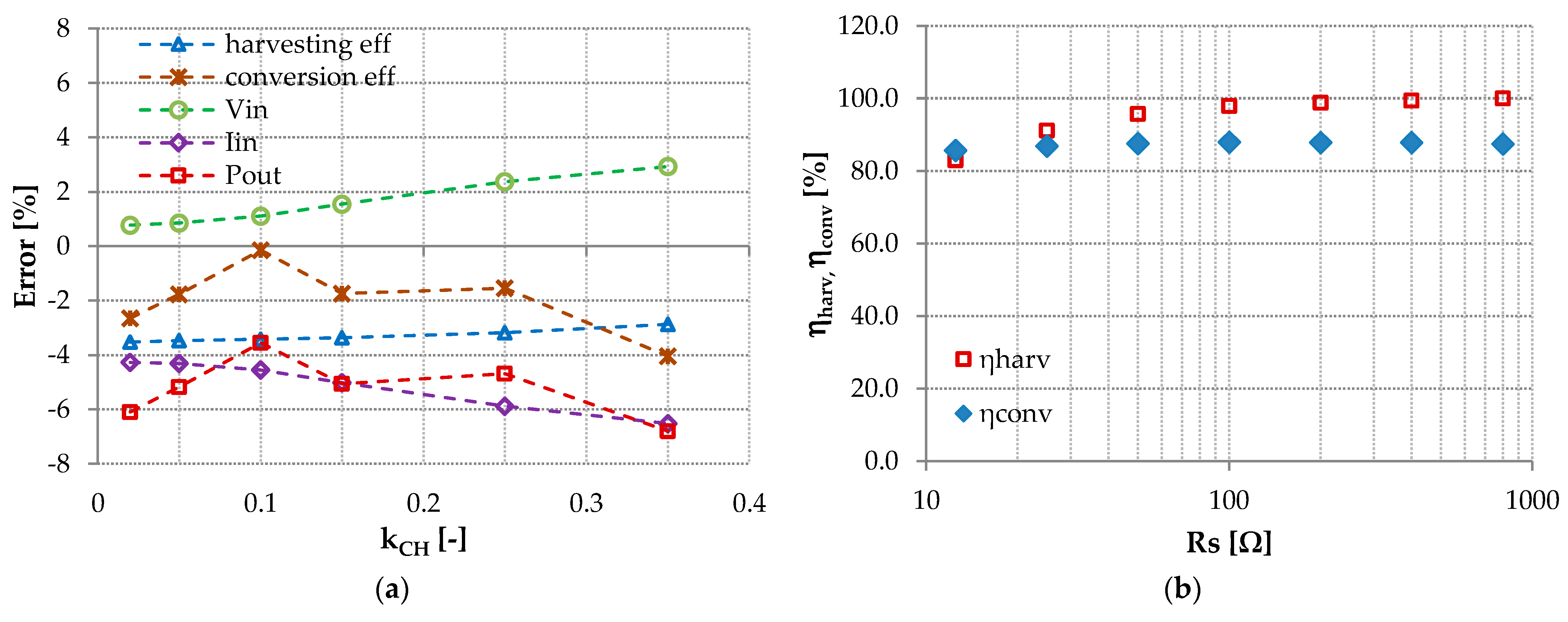
As shown earlier in Figure 11 and Figure 12, the effect of the kCH parameter on the converter’s operation is small within a certain range of change, as it is “compensated” by the calculated value of the kON parameter. Therefore, to make the Figure 23a more readable, it was decided to present the influence of the kCH parameter on the key quantities by means of an error relative to the values calculated in the simulations. Both the energy conversion efficiency factor ηconv and harvesting efficacy factor ηharv, agree reasonably well with the simulations, although both are again slightly lower than simulated values. The same observations apply to the output power given off to the battery and the load, which is very similar to the energy conversion efficiency factor ηconv. It is not surprising, as output power appears in the definition of energy conversion efficiency factor ηconv.
However, both the input voltage (average voltage across capacitor C) and input resistance slightly, but linearly, deviate from the simulation, which can be explained by the slight deviation of the actual values of capacitance C and inductance L and those entered in the microcontroller code.
The effect of source resistance on converter performance and parameters was also measured. The prototype was adapted to work with sources with resistances in the range of 50 Ω to 200 Ω (as in the example above), but even so, as can be seen in Figure 23b, even a much higher source resistance does not affect the performance of the converter at all. If the source resistance is less than 50 Ω, the converter performs noticeably worse, but this can be easily explained because Equation (50) is much less well satisfied.

8.2. Static Measurements with Disturbance

The proposed control algorithm assumes that the source parameters are measured every certain period derived from the source parameters. After these measurements, the device operates in maximum power transfer mode. It is only when the source parameters change significantly that the converter’s parameters may differ from the optimal values. As already mentioned, for real power sources the voltage changes much faster than the resistance. For these reasons, the prototype was tested by forcing the converter to operate with the open-circuit voltage used to calculate control parameters other than the actual one.
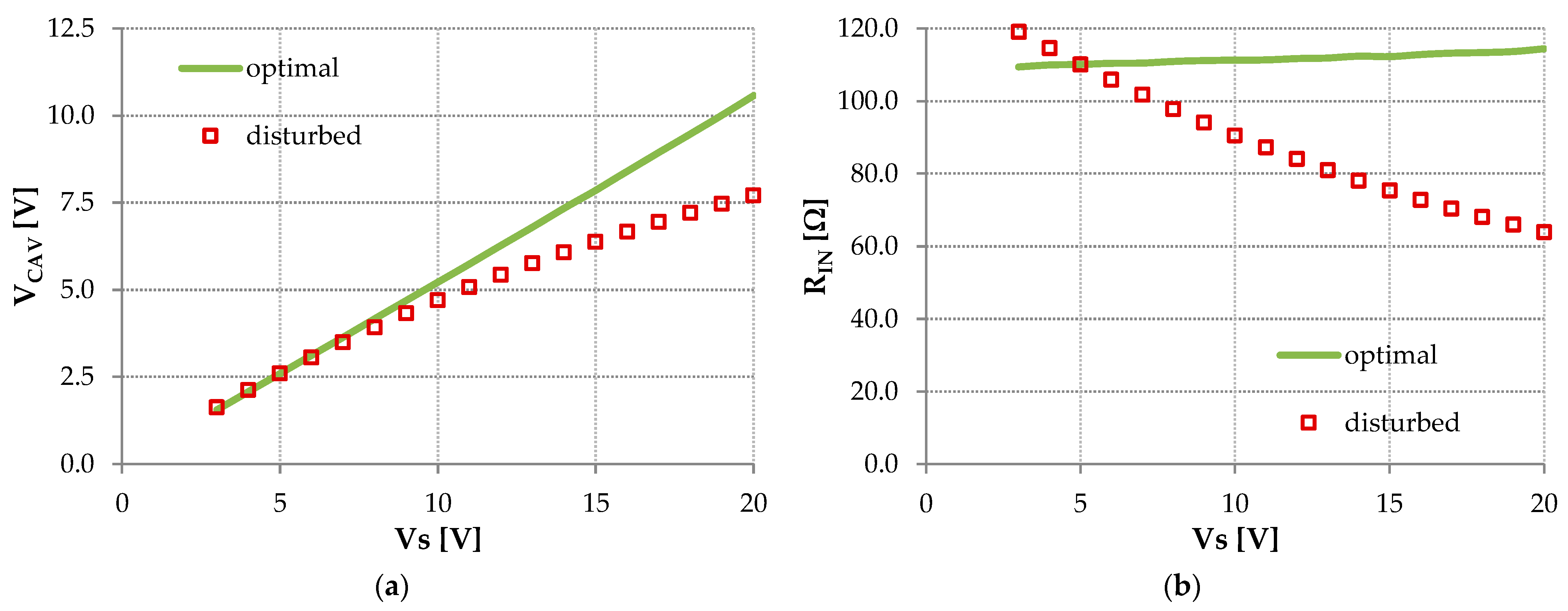
As can be expected, when the converter operates with an incorrect open-circuit voltage value, the output power energy, conversion efficiency factor ηconv, and harvesting efficacy factor ηharv are lower than when the converter operates with an exact open-circuit voltage value. However, in the worst case (for VS equal to 20 V), output power drops are less than 10%, as can be seen in Figure 24. This is to be expected, as knowing how control parameters kON and kCH affects conversion efficiency factor ηconv and harvesting efficacy factor ηharv (Figure 11 and Figure 12). Figure 25 confirms that the converter operates close to the maximum power transfer mode. Both, the average voltage across input capacitor C and the input resistance are up to 25% lower than they should be in maximum power transfer mode, and the input resistance drops to 60 Ω for higher values of VS. However, it must be strongly emphasized that this means a loss of only 6.25% of available power due to resistance mismatch.

8.3. Dynamic Measurements

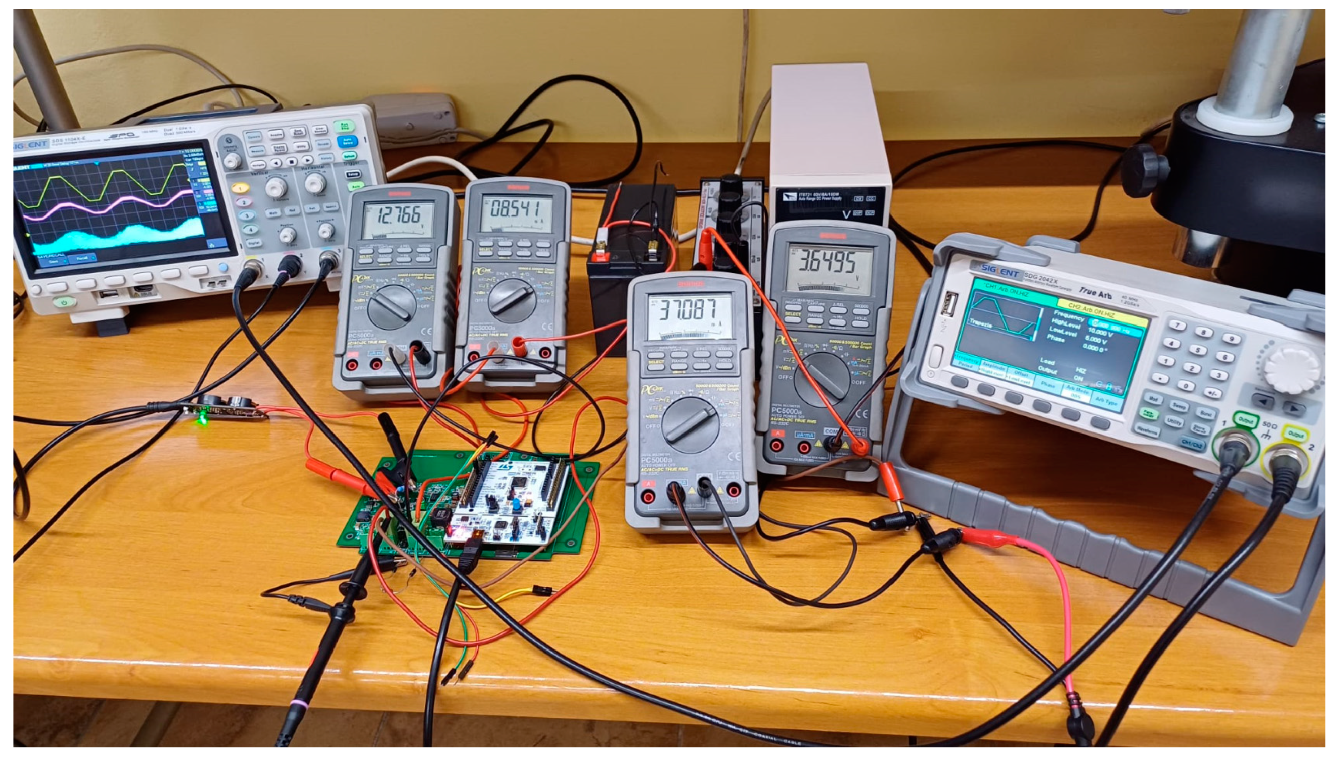
The converter was also tested in more realistic conditions. Siglent SDG2042X arbitral waveform generator replaced the power supply as an energy source, as shown in Figure 26. The AWG allowed to generate time-varying voltage VS from 0 V up to 10 V. It has an output resistance of 50 Ω, so in order to obtain an output resistance of 100 Ω, the decade resistor was set to 50 Ω. Since in this case, the open-circuit voltage is unavailable, the second channel of the AWG, with parameters duplicated from channel 1, was used to observe the open-circuit voltage. Apart from these changes the rest of the test bench remained the same.
During the test, the control algorithm used a fixed value of open-circuit voltage equal to 5 V, but the open-circuit voltage varied from 5 V to 10 V with a frequency of 10 Hz. This was conducted to simulate the rapid changes in open-circuit voltage between measurements.
As can be seen in Figure 27, although the open-circuit voltage increases twice, the input voltage of the converter, without recalculating the control parameters, roughly follows the open-circuit voltage. Thus, based on previous measurements, it can be concluded that the converter is operating almost in the maximum power transfer mode.
The last tests were to check the effect of frequency and, at the same time, the slew rate of open-circuit voltage on the operation of the converter. Figure 27 and Figure 28 show that both of these quantities have little effect on the operation and performance of the converter, even when the open-circuit voltage changes very rapidly.

9. Discussion

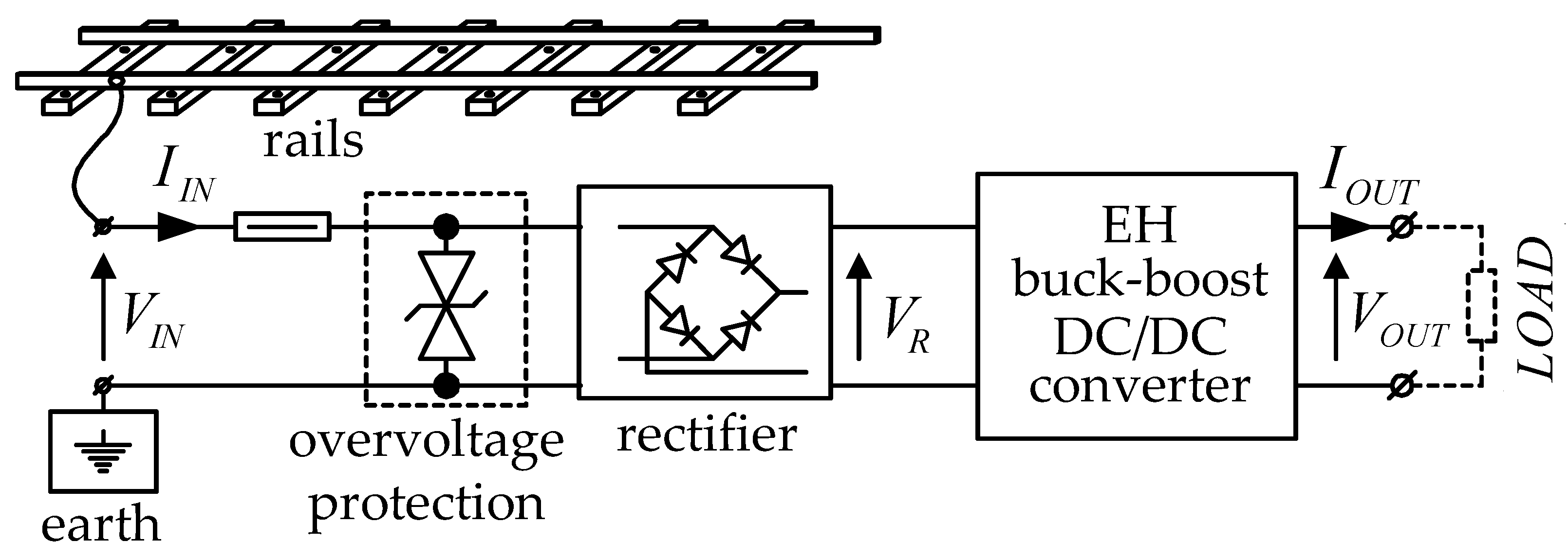
The device and its algorithm were designed to harvest energy from the stray currents of an electrified railroad line [1], so let’s consider how it could be applied in this case (Figure 29). In the case of harvesting energy from the stray currents, the open-circuit voltage is caused by the flow of a current along the not grounded rails, which means that the potential of the rail can be positive or negative. The source resistance depends on the rail-ground transition resistance, pins grounding resistance, and soil resistivity [1]. Expected RS values are in the range of 50–150 Ω. As previously mentioned, the rate of change of open-circuit voltage is usually less than 10 V/s and the source resistance usually changes much more slowly than 1 Ω/s. It implies it is enough to measure the open-circuit voltage and source resistance and update control parameters every 100 ms or so.
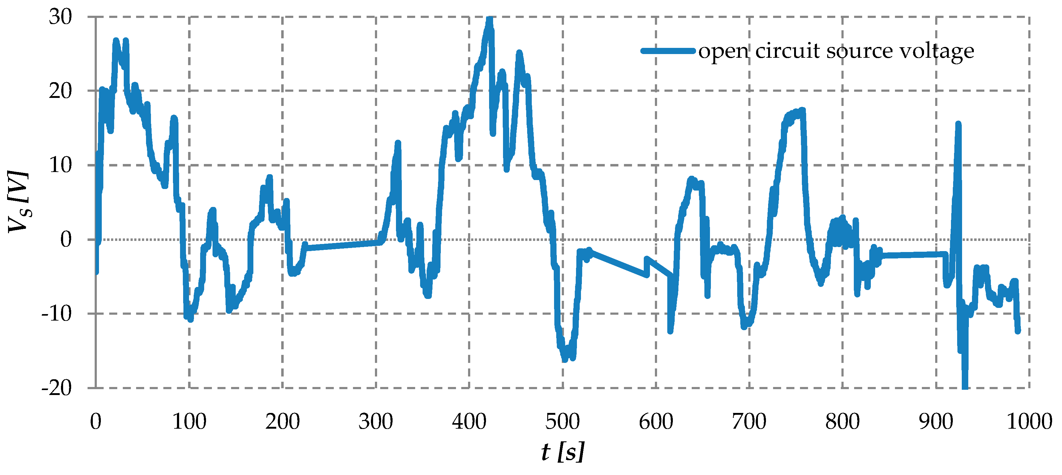
Since the potential of the rails in relation to the earth can be both positive and negative, as can be seen in Figure 30, it is necessary to use a rectifier before the converter described in this work. Secondly, the potential of the rails relative to the earth is rarely more than twice the voltage of a standard 12 V battery, resulting in the primary operating mode of such a converter being boost mode. For this reason, the simulations and measurements of the prototype device concerned the boost mode.
Although the proposed solution is designed to harvest energy from stray currents, it can also be used successfully with other energy sources with similar properties. The mathematical model of the converter shows that the impact of the output resistance is limited to a reduction in the available power, which means that the presented solution is potentially applicable even for sources with an output resistance greater than 1 kΩ.
The main limitation of the prototype is due to the use of a microcontroller, which means that the device itself consumes more power than converters designed as dedicated ICs. Therefore, the prototype is not suitable for harvesting energy from very low-power sources (less than 10 mW). However, implementing the proposed algorithm in a dedicated low-power IC could extend the range of applications to include weaker energy sources.
Table 1 contains a comparison of the prototype with other known converters that operate with energy sources with high output resistance. As mentioned above, described prototype requires greater input voltages than other converters but can operate with sources with much greater open-circuit voltage and can deliver much more power as well.

10. Conclusions

In this work, we presented the concept of a specialized converter that is able to efficiently harvest energy from sources that are characterized by high resistance and high variability of open-circuit voltage and output resistance. In particular, a novel control algorithm for the universal boost–buck converter has been proposed. Due to the high output resistance of the source, the maximum power transfer theorem was implemented. It should be emphasized that the presented solution does not use a negative feedback approach, but uses a feedforward control approach; the device is working with an open loop where control parameters and operating mode are periodically updated based on the analytical model and measured values of the resistance and open-circuit voltage of the source. The control signal frequency and duty cycle are calculated as well.
The model of the converter is finely verified by simulation and in a prototype device. To experimentally verify the concept a slightly modified previously designed device was used. So, it should be noted that the prototype was not fully optimized, and yet very encouraging results were achieved. The differences between measurements, simulations, and analytical results do not exceed 15% and can be explained by not taking into account secondary quantities such as the energy consumption of the control system from the battery or some parasite resistances absent in the mathematical model and simulations.
Detailed formulas for control parameters are derived and thorough design recommendations are provided, which should enable the proposed solution to be implemented quickly.

Author Contributions

Conceptualization, G.W., W.O. and Z.R.; methodology, G.W.; software, W.O.; validation, G.W., W.O. and Z.R.; formal analysis, G.W., W.O. and Z.R.; investigation, G.W., W.O. and Z.R.; resources, Z.R.; data curation, G.W., W.O. and Z.R.; writing—original draft preparation, G.W. and W.O.; writing—review and editing, W.O.; visualization, G.W., W.O. and Z.R.; supervision, Z.R.; project administration, Z.R.; funding acquisition, G.W., W.O. and Z.R. All authors have read and agreed to the published version of the manuscript.

Funding

This research was partially supported by the Polish Ministry of Education and Science funding for statutory activities (BK-250/RAU11/2024).

Data Availability Statement

Data are contained within the article.

Conflicts of Interest

The authors declare no conflicts of interest.

References

  1. Wieczorek, G.; Bernacki, K.; Rymarski, Z.; Oliwa, W. Gathering Energy of the Stray Currents in Electrified Railways Environment for Power Supply. Energies 2021, 14, 6206. [Google Scholar] [CrossRef]
  2. Xinyu, A.; Baowei, S.; Wenlong, T.; Congcong, T. Design and CFD Simulations of a Vortex-Induced Piezoelectric Energy Converter (VIPEC) for Underwater Environment. Energies 2018, 11, 330. [Google Scholar] [CrossRef]
  3. Carreon-Bautista, S.; Eladawy, A.; Nader Mohieldin, A.; Sánchez-Sinencio, E. Boost Converter With Dynamic Input Impedance Matching for Energy Harvesting With Multi-Array Thermoelectric Generators. IEEE Trans. Ind. Electron. 2014, 61, 5345–5353. [Google Scholar] [CrossRef]
  4. Jia, Y.; Yan, J.; Soga, K.; Seshia, A. Parametric resonance for vibration energy harvesting with design techniques to passivelyreduce the initiation threshold amplitude. Smart Mater. Struct. 2014, 23, 065011. [Google Scholar] [CrossRef]
  5. Gholikhani, M.; Nasouri, R.; Tahami, S.A.; Legette, S.; Dessouky, S.; Montoya, A. Harvesting kinetic energy from roadwaypavement through an electromagnetic speed bump. Appl. Energy 2019, 250, 503–511. [Google Scholar] [CrossRef]
  6. Kamuda, K.; Klepacki, D.; Sabat, W.; Kuryło, K.; Skoczylas, M.; Jankowski-Mihułowicz, P. Efficiency Measurements of Energy Harvesting from Electromagnetic Environment for Selected General Purpose Telecommunication Systems. Electronics 2024, 13, 3111. [Google Scholar] [CrossRef]
  7. Bandyopadhyay, S.; Chandrakasan, A.P. Platform Architecture for Solar, Thermal, and Vibration Energy Combining with MPPT and Single Inductor. IEEE J. Solid-State Circuits 2012, 47, 2199–2215. [Google Scholar] [CrossRef]
  8. Panizza, M. Input Source Impedance and Its Effects on DC-DC Converter Performance and Characteristics, Europe Applications Engineering, Vicor Corporation. Available online: https://www.vicorpower.com/documents/whitepapers/wp-input-source-impedance-DC-DC-VICOR.pdf (accessed on 30 November 2024).
  9. Middlebrook, R.D. Input Filter Considerations in Design and Application of Switching Regulators. In Proceedings of the IEEE Industry Applications Society Annual Meeting, Chicago, IL, USA, 11–14 October 1976; pp. 366–382. [Google Scholar]
  10. Siegers, J.; Domudala, V. How to Design Modular DC/DC Systems, Part 3: Stability Analysis and Decoupling. Available online: https://www.vicorpower.com/resource-library/tutorials/dc-dc-tutorials/dcdc-tutorial-3-stability (accessed on 30 November 2024).
  11. Input System Instability, SynQor, Application Note PQ-00-05-1 Rev. 2–23 August 2017. Available online: https://www.synqor.com/document-viewer?document=input+system+instability.pdf (accessed on 30 November 2024).
  12. Application Note 3166 Source Resistance: The Efficiency Killer in DC-DC Converter Circuits, Maxim Integrated. Available online: https://www.analog.com/en/resources/technical-articles/source-resistance-the-efficiency-killer-in-dcdc-converter-circuits.html (accessed on 30 November 2024).
  13. Di Maria, G. DC/DC Converters: Increasing Efficiency and Avoiding Bistability 23 March 2023. Available online: https://www.powerelectronicsnews.com/dc-dc-converters-increasing-efficiency-and-avoiding-bistability/ (accessed on 30 November 2024).
  14. Ramadass, Y.K.; Chandrakasan, A.P. A batteryless thermoelectric energy-harvesting interface circuit with 35mV startup voltage. In Proceedings of the 2010 IEEE International Solid-State Circuits Conference—(ISSCC), San Francisco, CA, USA, 7–11 February 2010; pp. 486–487. [Google Scholar] [CrossRef]
  15. Weng, P.-S.; Tang, H.-Y.; Ku, P.-C.; Lu, L.H. 50 mV-Input Batteryless Boost Converter for Thermal Energy Harvesting. IEEE J. Solid-State Circuits 2013, 48, 1031–1041. [Google Scholar] [CrossRef]
  16. Kim, J.; Kim, C. A DC–DC Boost Converter With Variation-Tolerant MPPT Technique and Efficient ZCS Circuit for Thermoelectric Energy Harvesting Applications. IEEE Trans. Power Electron. 2013, 28, 3827–3833. [Google Scholar] [CrossRef]
  17. Carlson, E.J.; Strunz, K.; Otis, B.P. A 20 mV Input Boost Converter With Efficient Digital Control for Thermoelectric Energy Harvesting. IEEE J. Solid-State Circuits 2010, 45, 741–750. [Google Scholar] [CrossRef]
  18. Umaz, R. Energy Harvesting System with A Single-step Power Conversion Process Achieving Peak Efficiency of 79.1%. In Proceedings of the 2020 International Congress on Human-Computer Interaction, Optimization and Robotic Applications (HORA), Ankara, Turkey, 26–28 June 2020; pp. 1–4. [Google Scholar] [CrossRef]
  19. Liu, X.; Sánchez-Sinencio, E. An 86% Efficiency 12 µW Self-Sustaining PV Energy Harvesting System With Hysteresis Regulation and Time-Domain MPPT for IOT Smart Nodes. IEEE J. Solid-State Circuits 2015, 50, 1424–1437. [Google Scholar] [CrossRef]
Figure 1. The considered series connection of the DC/DC converter to the source.
Electronics 14 00052 g001
Figure 2. Simplified input circuit of the energy harvesting device.
Electronics 14 00052 g002
Figure 3. A universal energy harvesting DC/DC converter. It should be very strongly emphasized that the VIB voltage, which is the voltage across the RSH resistor of value 0.1 Ω, is only used to monitor the output current; it is in no way used to control the converter, in particular, to implement negative feedback.
Electronics 14 00052 g003
Figure 4. The method of operation of the converter in boost mode: (a) Stage A—exponential capacitor C charging; (b) stage B—sinusoidal energy transferring from capacitor C to inductor L; (c) stage C—energy transferring to battery B from L and C; (d) waveforms in boost mode.
Electronics 14 00052 g004
Figure 5. The method of operation of the converter in buck mode: (a) Stage A—exponential capacitor C charging and transferring the energy to battery B; (b) stage B—sinusoidal energy transferring from capacitor C to inductor L; (c) waveforms in buck mode.
Electronics 14 00052 g005
Figure 6. The minimum value of inductance L vs coefficient kCH and normalized open-circuit voltage shown from two perspectives. Plotted using (54) assuming C and IMAX are equal to 1.
Electronics 14 00052 g006
Figure 7. The block diagram of the converter‘s control algorithm.
Electronics 14 00052 g007
Figure 8. Choice of operating mode: (a) comparison of harvesting efficacy defined by (63); (b) power delivered to the battery and load calculated using (57)–(60) for the circuit described in Section 7.
Electronics 14 00052 g008
Figure 9. The influence of the open-circuit voltage VS in boost mode on (a) the duty factor of the control signal; and (b) the frequency of the control signal normalized to the natural frequency of the LC circuit. The coefficient kCH was selected initially, and coefficient kON was calculated using (27) for VDmax = 13.8 V. The frequency hardly changes as the period of the control signal is approximately equal to TCH, which is constant. The legend on the left figure is valid for the right one as well.
Electronics 14 00052 g009
Figure 10. The influence of the open-circuit voltage VS in boost mode on (a) the duty factor of the control signal; and (b) the frequency of the control signal normalized to the natural frequency of the LC circuit. The coefficient kON was selected initially and coefficient kCH was calculated using (28) for VDmax = 13.8 V. The frequency and the duty factor depend almost linearly on open-source voltage VS as TCH is proportional to VS, and the period of the control signal is approximately equal to TCH.
Electronics 14 00052 g010
Figure 11. The influence of kCH or kON coefficients in boost mode on energy conversion efficiency factor ηconv shown from two points of view. Data calculated as described in Section 6.3 for the circuit described in Section 7. The legend in the middle is valid for both figures.
Electronics 14 00052 g011
Figure 12. The influence of kCH or kON coefficients in boost mode on energy harvesting efficacy factor ηharv shown from two points of view. Data calculated as described in Section 6.3 for the circuit described in Section 7. The legend in the middle is valid for both figures.
Electronics 14 00052 g012
Figure 13. The SPICE simulation circuit and directives for boost mode.
Electronics 14 00052 g013
Figure 14. A comparison of the simulation results with derived analytical relationships. The influence of the open-circuit voltage VS on (a) power delivered to the source POUT, data calculated using Formulas (57)–(60); (b) minimum VCL and maximum VCH voltage across capacitor C during one cycle in boost mode, data calculated using Formulas (18)–(20).
Electronics 14 00052 g014
Figure 15. The maximum current ILmax of the inductance L vs. the open-circuit voltage VS in different modes of operation and for different control modes (kCH = const or kON = const). Solid lines—data obtained using Formulas (8) and (35); markers—the results of the LTSpice simulation.
Electronics 14 00052 g015
Figure 16. The influence of key components tolerance and inaccuracy in determining source parameters on (a) the most important quantities describing the operation of the converter quantities; and (b) energy harvesting efficacy. Sensitivity is defined as the relative change of a given quantity from its nominal value (for nominal values of C, L, etc.).
Electronics 14 00052 g016
Figure 17. The schematic of the test bench used to measure prototype of the energy harvesting device. PC is the prototype of power converter and B is battery which together are Energy Harvesting Power Converter.
Electronics 14 00052 g017
Figure 18. The prototype of the energy harvesting device workingin the boost mode. On oscilloscope display: magenta waveform—Vin = VC, yellow waveform—K2 transistor control signal. Meters from left: VB [V], Iout [mA], IIN [mA], VCAV [V]. Source parameters: VS = 0.99 V, RS = 100 Ω.
Electronics 14 00052 g018
Figure 19. The most important waveforms of the converter working in the boost mode shown in two different time scales: yellow trace—K2 transistor control signal, magenta trace—voltage across capacitor C (Vin = Vc), green trace—voltage VD at the anode of diode D2, cyan trace—inductor L current measured on a 0.1 Ω resistor using differential probe. Source parameters: VS = 15 V, RS = 100 Ω. The set control parameter kCH = 0.1, calculated control parameters: kON = 0.188, f = 2.27 kHz, DF = 4.2%.
Electronics 14 00052 g019
Figure 20. The most important waveforms of the converter working in the buck mode shown in two different time scales: magenta waveform—Vin = VC, yellow waveform—K1 transistor control signal, green trace—voltage VD at the anode of diode D2, cyan trace—inductor L current measured on a 0.1 Ω resistor using differential probe. Source parameters: VS = 40 V, RS = 100 Ω.
Electronics 14 00052 g020
Figure 21. A comparison of the measurements of the prototype with simulations. The influence of the open-circuit source voltage VS on (a) energy conversion efficiency factor ηconv and harvesting efficacy factor ηharv; (b) output power. Source resistance RS was set to 100 Ω. The kCH parameter was set to 0.1.
Electronics 14 00052 g021
Figure 22. A comparison of the measurements of the prototype with simulations: (a) average voltage across input capacitor C changes vs. the open-circuit source voltage VS, source resistance RS = 100 Ω.; (b) input resistance vs. the open-circuit source voltage VS. Input resistance was calculated using VCAV/IIN, source parameters: VS = 15 V, RS = 100 Ω.
Electronics 14 00052 g022
Figure 23. The influence of (a) kCH parameter on several key quantities presented as a relative error compared to the values resulting from the simulations. Source parameters: VS = 15 V, RS = 100 Ω; (b) source resistance on energy conversion efficiency factor ηconv and harvesting efficacy factor ηharv. Open-circuit voltage VS = 10 V.
Electronics 14 00052 g023
Figure 24. A comparison of the measurements of converters operating with exact values of open-circuit voltage (‘optimal’ curves) with converters using fixed value VS equal to 5 V (‘disturbed’ curves): (a) energy conversion efficiency factor ηconv and harvesting efficacy factor ηharv; (b) output power. Measured in circuit presented in Figure 18. Source resistance RS was set to 100 Ω.
Electronics 14 00052 g024
Figure 25. A comparison of the measurements of converters operating with exact values of open-circuit voltage (‘optimal’ curves) with converters using fixed value of VS equal to 5 V (‘disturbed’ curves): (a) how average voltage across input capacitor C changes when the open-circuit source voltage VS is changing; (b) input resistance vs the open-circuit source voltage VS. Input resistance was calculated using VCAV/IIN. Source resistance RS = 100 Ω.
Electronics 14 00052 g025
Figure 26. The prototype of the energy harvesting device during quasi-realistic tests. On oscilloscope display: yellow waveform—open-circuit voltage VS from duplicated second channel of the AWG, magenta trace—input voltage VC, cyan trace—inductor L current measured on a 0.1 Ω resistor using differential probe. Meters from left: VB [V], Iout [mA], IIN [mA], VCAV [V]. Source parameters: open-circuit voltage VS varied from 5 V to 10 V, RS = 100 Ω.
Electronics 14 00052 g026
Figure 27. The most important waveforms of the converter during dynamic tests: yellow trace—open-circuit voltage VS from duplicated second channel of the AWG, magenta trace—input voltage VC, green trace—reference (GND) for VS and VC, cyan trace—inductor L current measured on a 0.1 Ω resistor using differential probe. Source parameters: RS = 100 Ω, VS changes from 5 V to 10 V with frequency: (a) 10 Hz; (b) 1 kHz. The control parameters calculated for 5 V, frequency of control signal was 2.323 kHz.
Electronics 14 00052 g027
Figure 28. A comparison of the measurements of converters operating with exact values of open-circuit voltage in static conditions (point at 0 Hz) with the converter using fixed value VS equal to 5 V while VS changes from 5 V to 10 V with frequency FS.
Electronics 14 00052 g028
Figure 29. Practical implementation of the proposed converter: the concept of a device for harvesting energy from stray current in an electrified railroad line. Note the rectifier required, as the voltage may be positive or negative to earth potential.
Electronics 14 00052 g029
Figure 30. Typical waveforms of the open-circuit voltage of the energy source when harvesting energy from a stray current in an electrified railroad line.
Electronics 14 00052 g030
Table 1. Comparison with known energy harvesters that work with sources with high output resistance.
Parameters[3][7][18]This Work
Energy sourceThermoelectric
generator
Thermoelectric
Generator, piezo-electric, photovoltaic
Thermoelectric
generator
Stray currents
Conversion-processBoost with impedance matching using MPPTBoost with impedance matching using MPPTTwo charge pumps, IC boost converter, supercapacitorBoost, flyback, or buck with battery and resistance matching using source and converter modelling
Input voltage20 mV–150 mV50 mV–10 V>0.3 V2 V–60 V
Source resistance33 Ω–2.7 kΩ5 Ω–150 kΩ100 Ω10 Ω–1 k Ω
Output voltage1.8 V–2.5 V1.8 V–2.5 V3.3 V12 V
Maximum output power360 µW
@ Vin = 0.14 V
2.5 mW
from photovoltaic
200 mW
@ Vin = 0.8 V
1.5 W
@ Vin = 24 V
Efficiency61%
@ POUT = 360 µW
83%
from photovoltaic
65%
@ POUT = 100 mW
85%
@ Vin = 19 V
Commentsaabc
Disclaimer/Publisher’s Note: The statements, opinions and data contained in all publications are solely those of the individual author(s) and contributor(s) and not of MDPI and/or the editor(s). MDPI and/or the editor(s) disclaim responsibility for any injury to people or property resulting from any ideas, methods, instructions or products referred to in the content.