Abstract
In this paper, D-band (110–170 GHz) frequency tripler module is presented using anti-parallel GaAs Schottky diode pair and waveguide-to-microstrip transitions. The anti-parallel diode pair is used as a nonlinear device generating harmonic components for Q-band input signal (33–50 GHz). The diode is zero-biased to eliminate the bias circuits and thus minimize the number of circuit components for low-cost hybrid fabrication. The anti-parallel connection of two identical diodes effectively suppresses DC and even harmonics in the output. Furthermore, the first and second harmonics of Q-band input signal are cut off by D-band rectangular waveguide. Input and output impedance matching networks are designed based on the optimum impedances determined by harmonic source- and load-pull simulations using the developed nonlinear diode model. Waveguide-to-microstrip transitions at Q- and D-bands are also designed using E-plane probe to package the frequency tripler in the waveguide module. The compensation circuit is added to reduce the impedance mismatches by bond-wires connecting two separate substrates. The fabricated frequency tripler module produces a maximum output power of 5.4 dBm at 123 GHz under input power of 20.5 dBm. A 3 dB bandwidth is as wide as 22.5% from 118.5 to 148.5 GHz at the input power of 15.0 dBm. This result corresponds to the excellent bandwidth performance with a conversion gain comparable to the previously reported frequency tripler operating at D-band.
1. Introduction
Millimeter-wave frequency band ranging from 30 to 300 GHz finds a lot of commercial and military applications such as high-speed wireless communications and high-resolution radar sensors, since it allows for wide bandwidth and small wavelength (10–1 mm). It is essential to develop the semiconductor-based devices or circuits generating high purity and high power signals for millimeter-wave communication and radar applications. Fundamental oscillators operating at millimeter-wave above 100 GHz have been introduced in the form of integrated circuits (ICs) using silicon CMOS or compound semiconductor technologies [1,2,3]. However, the fundamental oscillator ICs exhibit very limited output power and phase noise performance at millimeter-wave frequencies. This is caused by the transistors of which output powers are inversely proportional to the frequency. Another approach to generating millimeter-wave signals is to design frequency multipliers which extract the wanted harmonic frequency component generated by the non-linear devices for high-purity and low-frequency input signal, while rejecting the other unwanted harmonic frequency components [4].
Frequency multipliers can be designed using nonlinear semiconductor devices such as diodes or transistors. In millimeter-wave frequency above 100 GHz, GaAs Schottky diodes are commonly used for frequency multipliers, since they exhibit very high cut-off frequency and high output powers. It has another advantage in that it can be fabricated in the form of low-cost hybrid circuits [5]. In the frequency multipliers, it is important to filter out the spurious signals generated by the nonlinear devices, while amplifying the wanted harmonic component. In the diode-based frequency multipliers, the unwanted harmonic spurious can be effectively suppressed using the special connection of the diodes. The balanced type multipliers cancel out odd-order harmonic frequency components at the output by applying input signals with 180° out of phase to the diodes [6,7,8,9]. On the contrast, DC and even-order harmonic components are cancelled out at the output of anti-parallel diode pair which is thus widely applied for the design of millimeter-wave frequency triplers [10,11]. In order to reject the fundamental component, waveguide or microstrip filters can be placed at the input of the anti-parallel diode pair [12,13,14]. Power combiners in the waveguide are often employed to increase the output power at 3rd harmonic component [15,16].
In this work, we design a D-band (110–170 GHz) frequency tripler using anti-parallel pair of commercial GaAs Schottky diodes. We develop the nonlinear diode model using the datasheet provided by the vendor and electromagnetic simulations. Harmonic source- and load-pull simulations are performed using the develop nonlinear diode model to find the optimum impedances for high conversion gain. Input and output matching circuits are then designed to produce high 3rd harmonic power while rejecting the spurious signals. The frequency tripler is mounted inside the waveguide by designing the waveguide-to-microstrip transitions at the Q- and D-band using E-plane probes. The compensation circuit is also designed to minimize impedance mismatches caused by the bond-wires connecting the circuits in two separate substrates with different width for Q- and D-band transitions. In Section 2, the design of a D-band frequency tripler module is presented including diode model, impedance matching of frequency tripler, waveguide transitions, and bond-wire compensation circuit. Measurement results are given in Section 3, together with the performance comparison with other works.
2. Design of D-Band Frequency Tripler Module
2.1. GaAs Schottky Diode
We select GaAs Schottky diode (5VA30–13 by ACST) for the design of D-band frequency tripler in which three anodes are connected in series as illustrated in Figure 1 [17]. Figure 2a shows the equivalent circuit model of a single anode consisting of current source , junction capacitance , junction leakage conductance , and series resistance . The and are dependent on diode voltage as given in (1) and (2), where and are a saturation current and ideality factor, respectively [6]. In (2), and represent zero-bias junction capacitance and built-in voltage, respectively. The parameters of the equivalent circuit are extracted using the datasheet and measurement data provided by the vendor.
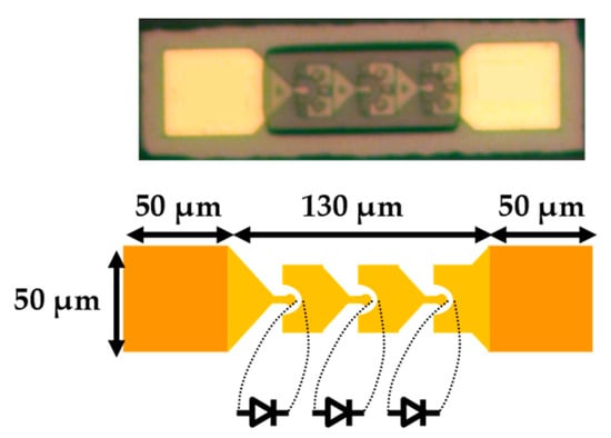
Figure 1.
GaAs Schottky diode (three-anodes in series).
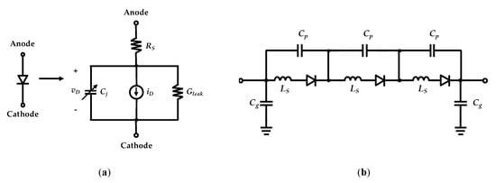
Figure 2.
Equivalent circuit model of diode. (a) Single anode and (b) three anodes in series.
Figure 2b shows the equivalent circuit of the three-anode diode including the parasitic series inductance and parallel capacitance in each anode. The pad capacitance on both ends is represented by [18]. These parasitic elements are extracted from the electromagnetic simulations and combined with the developed single diode model to complete three-anode diode model shown in Figure 2b. Table 1 shows the extracted parameters of the three-anode diode which are used for the design of frequency tripler.

Table 1.
Equivalent circuit parameters of three-anode diode.
2.2. Frequency Tripler Using Anti-Parallel Diode Pair
Anti-parallel diode pair shown in Figure 3 is a good choice for the design of odd-order frequency multipliers, since it allows in-phase combining of odd-order harmonic components of input signal and strongly suppresses the even-order harmonic components. The diodes can be reverse-biased for varactor-type frequency multipliers for high conversion gain [19]. In order to apply the reverse bias to the diodes, the bias circuit should be designed, consisting of the backside vias (or wire-bonding) for DC ground and capacitors for RF short. It can be easily designed and fabricated in ICs where the Schottky diodes and passive components are monolithically implemented on the GaAs substrate [15]. However, in the hybrid circuits, these additional off-chip circuit components introduce large parasitic effects at millimeter-wave frequencies, which can seriously degrade the performance. In addition, they can make overall circuit large and complicated, leading to high fabrication cost. Therefore, in order to alleviate these problems, we adopt the unbiased anti-parallel diode pair for the design of D-band frequency tripler in the hybrid circuit form as shown in Figure 3.
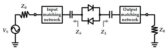
Figure 3.
Source- and load-pull simulations of anti-parallel diode pair.
In order to design the input and output matching network of the anti-parallel diode pair, the developed nonlinear diode model is used to determine the optimum impedance at each harmonic frequency. For this purpose, we perform harmonic source- and load-pull simulations as shown in Figure 3 [20]. From this simulation, we can find the optimum impedances presenting the maximum output power (Pout3) at 3rd harmonic frequency. Firstly, the load-pull simulation is performed to find load impedances ZL1 and ZL3 at fundamental (f0) and 3rd harmonic (3f0) frequencies, respectively, providing the highest Pout3. In this simulation, it is found that the impedances at 2f0 and 4f0 show almost no effect on the performance thanks to the anti-parallel connection of the diodes. Next, the source-pull simulation is performed to find source impedances ZS1 and ZS3, with ZL1 and ZL3 fixed to the values determined by the load-pull simulation. This process is iterated several times until the source and load impedances converge to optimum values. Figure 4 shows the source- and load–pull contours at input power of 19.0 dBm at f0 = 45 GHz. The highest Pout3 of 6.6 dBm is obtained at 3f0 = 135 GHz for the optimum source and load impedances specified in Table 2.
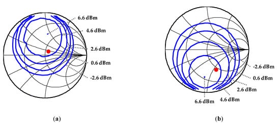
Figure 4.
Contours for 3rd harmonic power with step of 2 dB for input power of 19.0 dBm at f0 = 45 GHz. (a) Source-pull contours at f0. (b) Load-pull contours at 3f0.
Table 2.
Optimum impedances determined by source- and load-pull simulation.
Based on the source- and load-pull simulation results, input and output matching circuits are designed in a 5 mil-thick substrate with dielectric constant of 2.2 (RT Duroid 5880 by Rogers) as depicted in Figure 5. In the input matching network, three quarter-wave long lines at 3f0 (open stubs TL2 and TL3 and series line TL4) are employed to present high source impedance ZS3 to the anti-parallel diode pair. Then, high-impedance line TL1 is used to provide the optimum source impedance ZS1 at f0 given in Table 2. Two open stubs TL2 and TL3 also do the function of impedance matching at f0, presenting capacitive impedance. Output matching circuit is designed to provide slightly capacitive impedance at f0 and ZL3 at 3f0 given in Table 2. For this purpose, coupled line filter is designed at 3f0 to reject the fundamental components and provide the capacitive impedance at f0 together with transmission lines (TL5 and TL6). The low and high impedance lines, TL5 and TL6, respectively, are designed to present the optimum impedance at 3f0 as well. The source impedance at f0 and load impedance 3f0 of the designed matching network are represented by the red dots in the source- and load-pull contours in Figure 4, showing that they are close to optimum values determined by the source- and load-pull simulations.
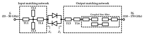
Figure 5.
Schematic of designed frequency tripler.
Figure 6 shows the simulated performance of the designed D-band frequency tripler. Output powers at each harmonic frequency are plotted in Figure 6a at input power of 19.0 dBm. Maximum Pout3 is 5.6 dBm at 138.9 GHz, corresponding to conversion gain of −13.4 dB. A 3 dB bandwidth is as wide as 22.9% (119.1–150.0 GHz). The fundamental power is suppressed by more than 13.7 dB compared to Pout3 within the 3-dB bandwidth. Note that it will be further rejected by the cut-off of D-band waveguide, when the frequency tripler is mounted in the waveguide. The 5th harmonic component is suppressed by 26.8 dB within the 3-dB bandwidth. The 2nd and 4th harmonic powers are less than −99 dBm in the simulation, so that they are not included in the figure. Figure 6b shows Pout3 and conversion gain depending on input power at f0 = 45 GHz. The conversion gain is saturated at −13.6 dB at input power of 22.0 dBm.
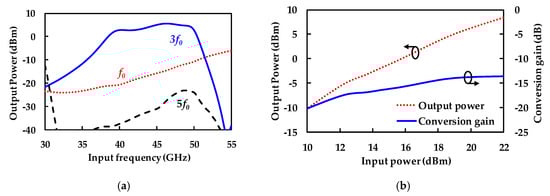
Figure 6.
Simulated performance of designed frequency tripler. (a) Output power versus frequency with input power of 19.0 dBm. (b) Output power and conversion gain versus input power at input frequency of 45 GHz.
2.3. Waveguide Transitions Using E-Plane Probe
The designed frequency tripler is mounted on the metal block with waveguide input and output. Therefore, waveguide-to-microstrip transitions are required at both Q- and D-band. Both transitions are designed using E-plane probe which translates TE10 mode of the rectangular waveguide to quasi-TEM mode of the microstrip line. Figure 7a shows Q-band waveguide-to-microstrip transition in the same substrate as used in the frequency tripler. The input impedance and bandwidth are mainly determined by the width (W) and length (L) of the probe and the distance (D) from the backshort [21]. The input impedance of the designed probe is matched to 50 Ω by adding quarter-wave long (λ/4) impedance transformer. Figure 8a shows the simulated results of the designed Q-band transition exhibiting insertion loss less than 0.1 dB and return loss better than 11.4 dB at full Q-band (33–50 GHz).
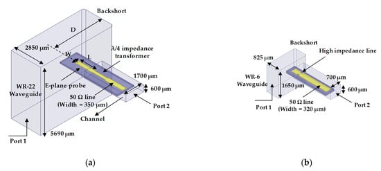
Figure 7.
Waveguide-to-microstrip transition using E-plane probe. (a) Q-band transition. (b) D-band transition.
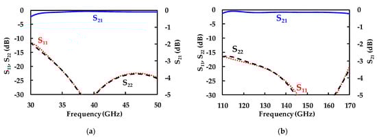
Figure 8.
Simulated S-parameters of the designed waveguide transition. (a) Q-band transition. (b) D-band transition.
Figure 7b shows the designed D-band waveguide-to-microstrip transition in the same way as Q-band transition. The probe is designed to have a slightly reactive impedance and then matched to 50 Ω by using high impedance line. The simulated insertion loss is less than 0.2 dB with return loss better than 16.4 dB across full D-band as shown in Figure 8b.
2.4. Compensation of Bond-Wire Effect
Transitions and frequency tripler are designed in the same substrate. However, as demonstrated in Figure 9, they are implemented using two separate substrates with different width, one for Q-band transition and frequency tripler (wide substrate) and the other for D-band transition (narrow substrate). This is because D-band transition should have a small width for good transition performance due to the small size of D-band waveguide. However, it is a bit difficult process to precisely cut out the substrate with non-square shape. Therefore, we fabricate the overall circuits in two separate substrates and then connect two signal lines using bond-wires as shown in Figure 9. (see Figure 12a as well). Unfortunately, the bond-wires exhibit high parasitic effect at millimeter-wave frequencies, so that it can cause severe impedance mismatches and performance degradation, unless they are properly compensated for [22,23].
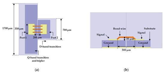
Figure 9.
Simulation of bond-wire effect. (a) Top view and (b) cross-sectional view.
Figure 9 shows the structure for the simulation of bond-wire effect. A gold wire with a diameter of 25 μm is used to connect two 50 Ω signal lines with the spacing of 200 μm. The wires are placed 35 μm higher from the substrate. Three parallel wires are used to minimize the parasitic inductance. Figure 10 shows the simulated S-parameters of this structure. Even though three short wires are used in parallel, the insertion loss is higher than 1.0 dB and return loss is below 10 dB at D-band, as shown in Figure 10a. The input impedance is plotted on Smith chart in Figure 10b, showing that bond-wires produce parasitic capacitive component at D-band (42.5-j36 Ω at port 1 and 51-j33.5 Ω at port 2, at 135 GHz).
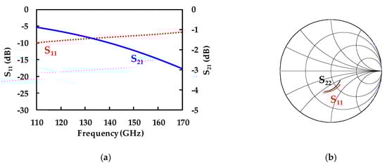
Figure 10.
Simulated S-parameters of bond-wires (a) in rectangular plot and (b) on Smith chart.
In order to compensate for the bond-wire effect and thus recover the performance, we insert high impedance lines at both ports (70 Ω line at port 1 and 100 Ω line at port 2) as shown in Figure 11a. These inductive lines effectively cancel out the capacitive parts generated by the bond-wires. Figure 11b shows that the designed circuit effectively compensates for the bond-wire effect and reduces impedance mismatches, providing insertion loss less than 0.6 dB and return loss better than 19.0 dB at full D-band.
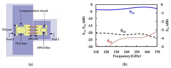
Figure 11.
Bond-wire compensation circuit. (a) Top view and (b) simulated results.
3. Measurement and Comparison
3.1. Measurement Results
Figure 12 is a photograph of fabricated D-band frequency tripler module including Q- and D-band transitions. Overall jig size is 50 mm × 50 mm × 50 mm.
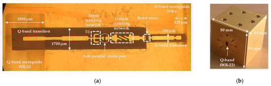
Figure 12.
Fabricated D-band frequency tripler module: (a) Internal view and (b) external view.
The fabricated waveguide-based frequency tripler is measued using the setup shown in Figure 13. Q-band signal is produced by a signal generator (E8257D by Keysight) followed by power amplifier (AMP-22-02070 by Millitech). D-band output power is measured by the power meter (PM5 by Erickson). Q-band input power is also measured by power meter (E4410B by Agilent) and power sensor (N8487A by Agilent) through a 10 dB coupler (22–3000/10 by Aerowave). D-band waveguide has a cut-off frequency of 90.8 GHz in the dominant TE10 mode, so that the fundamental and 2nd harmonic signals below the cut-off are rejected by D-band waveguide and thus they are not included in the measured output power.
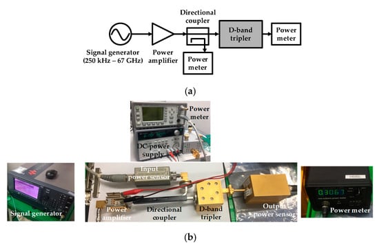
Figure 13.
Measurement set-up of D-band frequency tripler. (a) Block diagram and (b) photograph.
Figure 14a shows the measured output power versus output frequency at input powers of 15.0, 19.0 and 20.5 dBm. The maximum output power is measured to be 5.4 dBm at 123 GHz under input power of 20.5 dBm, corresponding to the conversion gain of −15.1 dB. A 3-dB bandwidth is 24.0 GHz from 118.5 to 142.5 GHz at input power of 20.5 dBm. The upper frequency of the bandwidth is limited to 142.5 GHz due to the driving capability of the Q-band power amplifier in the measurement setup. At the input power of 15.0 dBm, the measured 3-dB bandwith is as wide as 30.0 GHz from 118.5 to 148.5 GHz. Figure 14b shows the measured output power and conversion gain versus input power at f0 = 45 GHz. The maximum output power is 4.5 dBm at input power 21.5 dBm with conversion gain of −17.0 dB. The output power seems to be not satruated yet and is expected to increase at higher input power. Maximum conversion gain is measured to be −16.7 dB at input power of 19.5 dBm. The measurement shows 1.8–3.3 dB lower output power and conversion gain than the simulation, which seems to be caused by the losses of Q- and D-band transitions and inaccurate diode model.
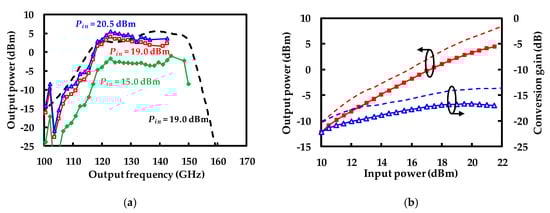
Figure 14.
Measured output power and conversion gain (solid: measurement, dashed: simulation). (a) Output power versus frequency at certain input powers (Pin). (b) Conversion gain and output power versus input power at output frequency of 135 GHz.
3.2. Performance Comparison
Table 3 compares the performance of the reported D-band frequency tripler modules using anti-parallel GaAs Schottky diodes. They are all mounted in the rectangular wavguides. The frequency triplers in [14] and this work were fabricated in the form of hybrid circuits using zero-biased diodes. In [15], the diodes were reverse-biased for high performance in the GaAs integrated circuit. The frequency tripler module in this work shows a 3-dB fractional bandwidth of 22.5% which is larger than those in [14,15]. It exhibits a peak output power of 5.4 dBm which is comparable to the zero-biased frequency tripler in [14].
Table 3.
Reported D-band frequency tripler modules using GaAs Schottky diodes.
4. Conclusions
In this work, the D-band frequency tripler module was presented using GaAs Schottky diodes and waveguide transitions. Un-biased anti-parallel diode pair was well-suited for the frequency tripler with simple structure, since even harmonic components are strongly suppressed at the output. In addition, the fundamental component is cut-off by the D-band waveguide. Harmonic load-pull simulations were performed using the developed nonlinear diode model to find the optimum impedances for high 3rd harmonic power. Bond-wire compensation circuit was carefully designed based on full-wave electromagnetic simulations. The measurement result showed the comparable performance to the previously reported D-band frequency tripler modules with excellent bandwidth. Therefore, the fabricated frequency tripler module can be used for millimeter-wave signal generation above 100 GHz.
Author Contributions
Conceptualization, J.D., J.K. and J.J.; methodology, J.D., J.K. and J.J.; software, J.D. and J.K.; validation, J.D.; formal analysis, J.D.; data curation, J.D.; writing—original draft preparation, J.J.; writing—review and editing, J.D. and J.J.; visualization, J.D.; supervision, J.J.; funding acquisition, J.J. All authors have read and agreed to the published version of the manuscript.
Funding
This work was supported by the Institute for Information & Communications Technology Planning & Evaluation (IITP) grant, funded by the Korean government (MSIT) (No. 2016-0-00185, Development of ultra-wideband terahertz CW spectroscopic imaging systems based on electronic devices).
Conflicts of Interest
The authors declare no conflict of interest.
References
- Cao, C.; Kenneth, K.O. A 140-GHz Fundamental Mode Voltage-Controlled Oscillator in 90-nm CMOS Technology. IEEE Microw. Wirel. Compon. Lett. 2006, 16, 555–557. [Google Scholar] [CrossRef]
- Kim, D.; Rieh, J. Comparison of Two Layout Options for 110-GHz CMOS LC Cross-Coupled Oscillators. J. Electromagn. Eng. Sci. 2018, 18, 141–143. [Google Scholar] [CrossRef]
- Kwon, Y.; Pavlidis, D.; Brock, T.L.; Streit, D.C. A D-Band Monolithic Fundamental Oscillator Using InP-Based HEMTs. IEEE Trans. Microw. Theory Tech. 1993, 41, 2336–2344. [Google Scholar] [CrossRef]
- Jun, J.; Bin, L.; Li, M.; Yue, H.; Xiangyang, S.; Yaoling, T.; Hailong, H.; Fengjun, C.; Xianjin, D.; Jian, Z. Single-Stage Frequency Quadrupler with SBD and Four-Octave LPF at 335 GHz. IEEE Trans. Terahertz Sci. Technol. 2017, 7, 446–454. [Google Scholar] [CrossRef]
- Pozar, D.M. Microwave Engineering, 4th ed.; Wiley: New York, NY, USA, 2011; pp. 525–530. ISBN 978-0470631553. [Google Scholar]
- Zhang, B.; Ji, D.; Min, Y.; Fan, Y.; Chen, X. A High-Efficiency 220 GHz Doubler Based on the Planar Schottky Varactor Diode. J. Electron. Mater. 2019, 48, 3603–3611. [Google Scholar] [CrossRef]
- Porterfield, D.W.; Crowe, T.W.; Bradley, R.F.; Erickson, N.R. A High-Power Fixed-Tuned Millimeter-wave Balanced Frequency Doubler. IEEE Trans. Microw. Theory Tech. 1999, 47, 419–425. [Google Scholar] [CrossRef]
- Chattopadhyay, G.; Schlecht, E.; Ward, J.S.; Gill, J.J.; Javadi, H.H.S.; Maiwald, F.; Mehdi, I. An All-Solid-State Broad-Band Frequency Multiplier Chain at 1500 GHz. IEEE Trans. Microw. Theory Tech. 2004, 52, 1538–1547. [Google Scholar] [CrossRef]
- Montero-de-Paz, J.; Sobornytskyy, M.; Hoefle, M.; Cojocari, O. High Power 150 GHz Schottky based Varactor Doubler. In Proceedings of the 2016 Global Symposium on Millimeter Waves (GSMM) & ESA Workshop on Millimeter-Wave Technology and Applications, Espoo, Finland, 6–8 June 2016. [Google Scholar] [CrossRef]
- Dou, J.; Xu, J.; Jiang, S. Accurate Design of a W-band Full Band Frequency Tripler Based on Anti-parallel GaAs Schottky Varistor Diode Pair. In Proceedings of the 2017 Progress Electromagnetics Research Symposium, St Petersburg, Russia, 22–25 May 2017; pp. 3809–3811. [Google Scholar] [CrossRef]
- Liu, Y.; Zhao, M.; He, Z.; Zhu, Z. A High Efficiency Balanced Frequency Tripler Incorporating Compensation Structure for Millimeter-Wave Applications. Prog. Electromagn. Res. C 2015, 59, 79–88. [Google Scholar] [CrossRef]
- Jha, P.; Basu, A.; Koul, S.K. Broadband Frequency Tripler Design at 40–60 GHz. In Proceedings of the Asia-Pacific Microwave Conference 2016, New Delhi, India, 5–9 December 2016. [Google Scholar] [CrossRef]
- Mao, W.; Yu, M.; He, Y. Design of Submillimeter Wave Frequency Tripler. In Proceedings of the 2009 Asia Pacific Microwave Conference, Singapore, 7–10 December 2009; pp. 1188–1191. [Google Scholar] [CrossRef]
- Guo, C.; Shang, X.; Lancaster, M.J.; Xu, J.; Powell, J.; Wang, H.; Alderman, B.; Huggard, P.G. A 135–150 GHz Frequency Tripler With Waveguide Filter Matching. IEEE Trans. Microw. Theory Tech. 2018, 66, 4608–4616. [Google Scholar] [CrossRef]
- Siles, J.V.; Lee, C.; Lin, R.; Chattopadhyay, G.; Reck, T.; Jung-Kubiak, C.; Mehdi, I.; Cooper, K.B. A High-Power 105–120 GHz Broadband On-Chip Power-Combined Frequency Tripler. IEEE Microw. Wirel. Compon. Lett. 2015, 3, 157–159. [Google Scholar] [CrossRef]
- Chen, Z.; Xu, J. Design and characterization of a W-band power-combined frequency tripler for high-power and broadband operation. Prog. Electromagn. Res. 2013, 134, 133–150. [Google Scholar] [CrossRef][Green Version]
- Jin, M.; Dehai, Z.; Changhong, J.; Xin, Z.; Jian, H.; Dashuai, Y. Crucial problems in the design of a terahertz tripler. J. Semicond. 2015, 36, 085003. [Google Scholar] [CrossRef]
- Hoefle, M.; Penirschke, A.; Cojocari, O.; Jakoby, R. Advanced RF Characterization of New Planar High Sensitive Zero-Bias Schottky Diodes. In Proceedings of the 2011 6th European Microwave Integrated Circuit Conference, Manchester, UK, 10–11 October 2011; pp. 89–92. [Google Scholar]
- Porterfield, D.W. High-Efficiency Terahertz Frequency Triplers. In Proceedings of the 2007 IEEE/MTT-S International Microwave Symposium, Honolulu, HI, USA, 3–8 June 2007; pp. 337–340. [Google Scholar] [CrossRef]
- Jeong, J.; Jang, D. Design Technique for Harmonic-Tuned RF Power Oscillators for High-Efficiency Operation. IEEE Trans. Ind. Electron. 2015, 62, 221–228. [Google Scholar] [CrossRef]
- Donadio, O. G-Band Waveguide to Microstrip Transition for MMIC Integration. Ph.D. Thesis, Dept. Science and Engineering, Glasgow Univ., Glasgow, UK, January 2012. [Google Scholar]
- Alimenti, F.; Mezzanotte, P.; Roselli, L.; Sorrentino, R. An Equivalent Circuit for the Double Bonding Wire Interconnection. In Proceedings of the IEEE MTT-S International Microwave Symposium Digest, Anaheim, CA, USA, 13–19 June 1999; pp. 633–636. [Google Scholar] [CrossRef]
- Doo, J.; Park, W.; Choe, W.; Jeong, J. Design of Broadband W-band Waveguide Package and Application to Low Noise Amplifier Module. Electronics 2019, 8, 523. [Google Scholar] [CrossRef]


© 2020 by the authors. Licensee MDPI, Basel, Switzerland. This article is an open access article distributed under the terms and conditions of the Creative Commons Attribution (CC BY) license (http://creativecommons.org/licenses/by/4.0/).