Abstract
This work proposes a high-performance asymmetric gold/graphene/platinum photodetector. The new photodetector, operating without bias, integrates interdigitated 100 nm spaced metallic contacts that induce a built-in potential and a short carrier path, allowing an improvement in the separation and collection of the photocarriers. A chemical vapor deposition graphene layer is transferred onto the interdigitated electrodes elaborated using high-resolution electron-beam lithography. Three devices with different side dimensions (100, 1000, and 3000 µm) are fabricated, and their photoresponsivities are evaluated at different wavelengths. The 100 µm device shows the highest photoresponsivity of 358 A/W at a 400 nm illumination. These promising results confirm the proposed design’s ability to increase the photodetector’s active area, improve light absorption, and achieve high separation and collection of photogenerated carriers. This makes it of great interest for optoelectronic applications.
1. Introduction
Graphene is a single layer of carbon atoms arranged in a honeycomb lattice [1,2,3,4]. The extremely high mobility of the photogenerated carriers [3,5,6,7], the flat light-absorption spectrum [6,8,9], high flexibility [10], and high conductivity [8,11,12,13] of graphene have attracted increasing attention for wide-range wavelength photodetector applications [14,15], despite the emergence of several new two-dimensional (2D) materials, including transition metal dichalcogenides (TMDs) [16,17] and black phosphorus [18]. However, the use of graphene in photodetectors has been limited due to its small photo absorption [8] and extremely short carrier lifetime [19,20,21,22,23]. To overcome the shortcomings of graphene—and considering the efficiency of graphene/semiconductor interfaces for generating, separating, and transmitting photocarriers—hybrid graphene/semiconductor heterojunctions were proposed and demonstrated by combining zero-dimensional quantum dots, one-dimensional nanowire semiconductors, and other two-dimensional layered materials [24,25,26,27,28]. Despite the device’s improved quantum efficiency, its absorption band was determined by the material added, losing the intrinsic advantage of graphene’s broad spectral photoelectric response [15]. Due to graphene’s short carrier lifetime, the only generated photocarriers in graphene that can contribute to the photocurrent are those near the metal contacts [29,30]. This problem can be resolved by fabricating interdigitated electrodes (IDEs), providing a larger photoabsorption area [31,32,33], and increasing the number of photogenerated carriers responsible for photocurrent generation. Several metals can be used as electrodes with symmetric or asymmetric configurations. Graphene-based photodetectors using the same metals on both electrodes are restricted by the symmetric band structure and field profile in the channel or between two adjacent fingers. Thus, the net photocurrent will not flow unless a drain bias is applied, because the photocarriers generated on the source and drain side have opposite charges and are compensated in the center of the graphene channel [23,31,34,35]. For this reason, many researchers have proposed photodetectors based on graphene with different metal contacts for electrodes, including gold/palladium, gold/aluminum, and gold/titanium [31,34,35,36,37]. Asymmetric contact electrodes with different work functions induce a strong built-in potential across the graphene that imparts apparent photovoltaic activities to the devices and allow them to act as self-driven photodetectors [38,39].
On the other hand, it has been found that contacts on the bottom of graphene yield resistivities four times lower than contacts on top of graphene [40,41]. The bottom electrode structure has significantly reduced contact resistivity due to the direct contact of graphene with high work function metal, fewer side effects during the fabrication process, and improved density of states at the Dirac point of the graphene edges. This architecture was proposed to achieve a lower resistance than traditional metal-on-top contact. This reduction was attributed to the cleaner interface between graphene and metals obtained by the metal-on-bottom process. It has been found that growth defects in graphene film also reduce the resistivity by a factor of two [41], contributing to an increase in the photocurrent.
Reducing the distance between the metal fingers can also increase the photocurrent [31,42]. In graphene photodetectors, the built-in field extends to several 100 nm wide at the interface where the charge transfer between metal and graphene takes place [43], and the absolute magnitude of the photocurrent is relatively small (in the nA range). For these reasons, at most, a finger gap of 100 nm is required. A small gap size (100 nm) can significantly enhance the light–graphene interaction and, thus, increase the light absorption in graphene. This is because the incident light is concentrated in these nanogaps between the electrodes, and the nanogap dimension is smaller than 𝜆/2 of light [44,45]. This design can greatly enhance the light–graphene interaction (absorption) and bypass the short carriers’ lifetime in the graphene layer by collecting all generated photocarriers in the region within the source and the drain, thanks to the size of the fingers nanogap (100 nm) [34,46]. The 100 nm gap can be achieved using nanolithography, and it represents a trade-off between the response time and the difficulty of the lithographic process. The aspect ratio reduction cannot be pursued below a certain value because it could cause a significant increase in the photodetector series resistance, particularly for larger sizes up to 3000 µm. Yoo et al. studied asymmetric metals’ contact with gold (Au) and titanium (Ti) and reported a maximum photoresponsivity of 52 mA/W [34].
Choosing the right synthesis method is another critical step in fabricating graphene-based electronic devices. Many approaches are used to synthesize graphene for electronics applications, including mechanical exfoliation from highly oriented pyrolytic graphite using a ribbon, epitaxial growth on silicon carbide (SiC) substrate, and chemical vapor deposition (CVD) [47]. However, mechanical exfoliation is not an alternative when a large graphene area is required. Graphene on centimeter-sized copper substrates or SiC wafers paves the way for the large-scale production of high-quality graphene sheets for a wide range of industrial applications [48]. Graphene grown on SiC wafers has the advantage of growing natively on a transparent insulating substrate, which enables the transfer-free fabrication of optoelectronic devices. However, graphene epitaxially grown on a SiC substrate is hardly transferrable, it is too expensive for mass production, and its film size is limited by the SiC substrate. Thanks to its low cost and high versatility, CVD is the most popular technique that can scalably produce graphene, allowing it to be transferred to virtually any type of substrate.
Transferring graphene is also an essential step in the fabrication of graphene devices. Aside from automated, continuous transfer systems [49], which are not yet generally accessible, wet graphene transfer limitations are largely user-related and require a trained hand to get reproducible outcomes. The etching process for Cu-containing metallic particles (from the FeCl3 solution) and the removal and rinsing of PMMA residues are two major sources of contamination. CVD graphene exhibits both p-type doping and electrical property degradation due to these contaminations [50,51]. In order to dissolve the metallic contamination from etchants such as FeCl3, PMMA-coated graphene has been rinsed in DI water solution with 1–2% HCl [52]. In the process of dissolving the copper foil, air bubbles can cause undissolved copper clusters. To remove the Cu clusters more effectively, fresh FeCl3 solutions can be used, followed by sequential dissolutions. Regardless, small Cu atom clusters and ions always appear on the graphene surfaces after transfer. As these particles occur on the top side of graphene (most residues are trapped at the substrate-graphene interface), they should not affect graphene surface processes. In order to guarantee a reliable transfer at a negligible contamination level, even without any post-treatment at high temperatures, an anisole mixture balancing the average molecular weight and weight percentage in PMMA was developed by Liao et al. [53].
In most studies, the graphene used in photodetectors is made by mechanical exfoliation because it yields the best quality graphene. Electrodes are made on top of graphene because of their ease of fabrication. However, few reports investigate the use of chemical vapor deposition (CVD) techniques to fabricate graphene-based photodetectors with asymmetric interdigitated electrodes. In this context, the present work used a combination of CVD graphene, asymmetric IDEs, and 100 nm spaced adjacent fingers to achieve a metal/graphene/metal heterojunction that offers greater optical absorption enhancement and improves the collection of the generated photocarriers. Au and Pt, with different work functions, create an internal field that enables photodetection over the entire device area. This allows the devices to sum the individual contributions to the total photocurrent and operate the detector without applying an external drain-source bias. This is a significant advantage compared to the symmetrical electrodes used in a graphene detector reported by Ye et al., where a photoresponsivity of 4.6 mA/W was achieved, and required an external bias of −4 V to work [54]. Three devices with different side dimensions (100, 1000, and 3000 µm) were fabricated, and a comparative study as a function of the device’s dimensions is presented. This device’s architecture leads to high photoresponse that extends from the visible to the IR.
2. Materials and Methods
2.1. Fabrication of the Interdigitated Nanogap Electrodes
High-resolution electron-beam lithography (Vistec EBPG5200 100 kV, Vistec Electron Beam GmbH, Jena, Germany) was used to fabricate the interdigitated electrodes. Resist patterning with EBL is an attractive, highly automated method, allowing good flexibility in layout design, as well as a precisely controlled pattern with direct writing and an intrinsically high nanoscale resolution [55,56]. The main manufacturing process is shown schematically in Figure 1. The IDEs mask was designed using the libreCAD software, as shown in Figure S1. Two contacts were added at the device’s top right corner, as shown in Figure S1b. Three square devices with side dimensions of 100, 1000, and 3000 µm were prepared.
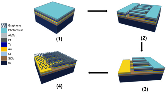
Figure 1.
The fabrication steps of the graphene photodetector interdigitated electrodes device: (1) deposition of all the metals and the photoresist; (2) lithography and ion milling; (3) second lithography and ion milling of Pt metal; (4) graphene transfer.
The IDE devices were fabricated on a boron-doped silicon substrate with a 100 nm SiO2 layer (from Swansea). The experimental process started by cleaning the silicon dioxide wafer using acetone and isopropanol. Then, 9 nm of chromium (Cr) was deposited on the wafer as an adhesion layer for metals, followed by 20 nm of Au. The reason for this is that this material has the ability to adhere well to common substrate materials, such as Si or SiO2. At the same time, thin layers of Cr (5–10 nm) typically have no effect on the fabricated device’s properties. The sites in the thin adhesion layer also aid in the nucleation of the next deposited material, which would otherwise not stick. In fact, platinum (Pt) and gold (Au) could not be used without an adhesion layer; they flake away from the sample. For the second finger set, to avoid the intermixing and the diffusion of Pt atoms into the Au layer during the deposition process, an appropriate barrier layer material is required. Tantalum (Ta), which has excellent thermal stability and good electrical conductivity, was deposited at 3 nm, followed by platinum (Pt) at 20 nm. Finally, 10 nm of aluminum trioxide (Al2O3) was deposited on top of the device using physical vapor deposition (PVD).
To remove organic and inorganic contaminants and improve the photoresist adhesion, a hydrophobic surface was achieved using low-temperature oxygen plasma etching for 6 min. A wet etch was afterward performed using tetramethylammonium hydroxide (TMAH) to remove the damage caused by the dry etch. The sample was then kept under an hexamethyldisilazane (HMDS) atmosphere for 15 min in a desiccator (Vapor Prime Oven YES-310TA, Yield Engineering Systems, Livermore CA, USA) to help the photoresist adhesion. The spin coating of the resist was performed immediately after the HMDS treatment. A negative resist was used; the layer to be etched was relatively thin (56 nm). Therefore, a photoresist layer of 80 nm was sufficient. Finally, the sample was inserted into the EBL machine.
2.2. CVD Growth and Transfer of Graphene
Graphene was grown on a 25 µm thick copper foil (purity > 99.99 wt.%) by chemical vapor deposition in a quartz tube 3-zone furnace (FirstNano EasyTube®3000, CVD Equipment Corporation, Central Islip, NY, USA). A gaseous mixture of methane/hydrogen was used during the growth process. Graphene transfer on the IDE device started by spin-coating a polymethyl methacrylate (PMMA) layer on the as-synthesized graphene/copper film. Then, the PMMA/graphene/copper film was floated on a 0.5 M ferric chloride solution for 2 h to etch the copper foil. After completely removing the copper, the PMMA/graphene film was soaked in an HCl solution for 30 min and then rinsed in deionized water for 10 min. The films were transferred to the device and air-dried overnight. Finally, the PMMA/graphene/IDEs device was placed in an acetone bath for 3 h to remove the PMMA.
2.3. Characterization
A Raman spectrophotometer (Alpha300 R Confocal Raman System, WITec GmbH, Ulm, Germany) with a 532 nm laser was used to measure the Raman spectra of graphene. Simultaneously, this Raman spectrophotometer was used to perform 40 × 40 µm2 Raman mapping of the position-G band (Pos (G)) and position of 2D band (Pos (2D)) of graphene. The objective used was 50× (Zeiss EC Epiplan, Zeiss, Oberkochen, Germany), and the motorized stage was used to scan the sample. Scanning electron microscopy (SEM), high-resolution SEM Quanta 650 FEG ESEM (FEI, Hillsboro, OR, USA), was used to study surface features and provide an energy-dispersive X-ray spectroscopy (EDX) analysis. For the electrical properties, IV curves of all devices (graphene) for different dimensions were measured with a source meter (Keithley 6470, Keithley Instruments, Solon, OH, USA) under ambient conditions. For all devices, IV curves were recorded in the dark and in the light for voltages between −3 and 3 mV for different wavelengths in the visible range. For these experiments, the light power was calibrated by a silicon photodetector.
3. Results and Discussion
During the lithography process, prior dose testing is required due to the high density of the pattern. The effect of the E-beam dose was examined to obtain the appropriate dose for the electrode’s width and spacing of 100 nm. Dose tests have been repeated, with proximity effect correction activated. The dose tests were carried out with three different doses (550, 617, and 683 µC cm−2). After developing, the sample’s relief was examined using a scanning electron microscope (SEM) to determine the appropriate nominal dose to obtain the required profile. Figure 2 shows SEM images of devices; the best doses were 550 and 617 µC cm−2. For the full exposure, the dose was set to 583 µC cm−2, an intermediate value between 550 and 617 µC cm−2.
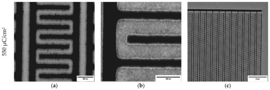
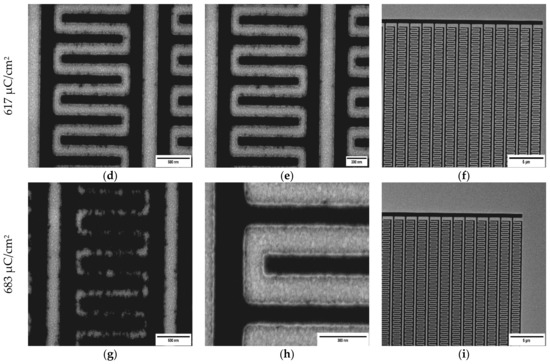
Figure 2.
Scanning electron microscope (SEM) images at the center (a,d,g), edge (b,e,h), and overview (c,f,i) of the devices for 550 µC cm−2, 617 µC cm−2, and 683 µC cm−2 doses, respectively.
A Nordiko 7500 ion milling machine (Hampshire, UK) performed the physical etching at 130° (40° from normal incidence). A second EBL procedure was used to complete the fabrication of the device. As shown in Figure 3, the second exposure was successful, and the bottom left corner of the devices has the best alignment, as it was exposed first.
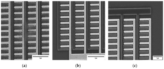
Figure 3.
SEM images of the device after the second EBL (a) at the center; and (b,c) at the edge.
Figure S2 shows optical images of the devices before and after the second ion milling process. Note that the zone in the bottom is an area that was protected with tape during the first ion milling, to give some signal in the second ion milling.
The SEM analysis in Figure 4a,b was collected after oxygen plasma ashing and 13 min of resist stripping. They show the presence of both areas (Au and Au/Pt) with different contrasts. Figure 4c shows the EDX analysis of the Au/Pt and Pt zones. The peaks of Au and Pt are very close and difficult to distinguish. Cr and Ta cannot be seen because of their small thickness (2–3 nm).
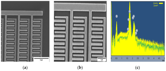
Figure 4.
(a,b) SEM images of the device edge after oxygen plasma ashing and 13 min of resist stripping; and (c) EDX of Au/Pt and Pt zones.
Ion milling was performed for 20 s to ensure the roughness of the samples had not increased. Figure 5a,b shows scanning electron microscopy (SEM) images of the fabricated IDEs after this cleaning. Figure S3 shows that, in comparison with Figure S2b, the color of the pads is changed, which could be due to the removal of the Ta layer. The SEM images show clear and uniform nanogaps, confirming the successful fabrication of the IDE arrays. The IDE devices are then ready for the graphene transfer.
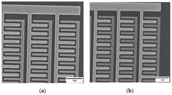
Figure 5.
(a,b) SEM images of IDEs after the final fabrication step.
Figure 6 shows the Raman spectrum of the graphene sample grown by CVD after being transferred onto the top of the electrodes. Raman spectroscopy was performed under a laser excitation of 532 nm (1.8 mW laser power), with an acquisition time of 10 s and a 600 groove/mm grating. The first two intense peaks at ca. 1596 and 1347 cm−1 correspond to graphene’s characteristic G and D bands [57,58]. The G peak corresponds to the E2g phonon at the center of the Brillouin zone [59]. The D peak is due to the breathing modes of six-atom rings and requires a defect for its activation [60,61]. The peak at 2686 cm−1 corresponds to the 2D band (also referred to as G’), and is the second order of the D peak [62]. Figure S4a,b shows the peak position maps of the G band (~1590 cm−1) and 2D band (from 2685 to 2688 cm−1), respectively [63,64]. The I2D/IG intensity ratio was about 2.6. The Raman ID/IG value was 0.6, and the full width at half maximum (FWHM) of the 2D band was measured to be 42 and 21 cm−1 for the G band. All these Raman properties confirm that the used film is monolayer graphene with some structural disorder [65].
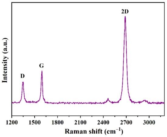
Figure 6.
Raman spectrum of a graphene sample grown by a CVD.
To determine the photon-to-electron conversion efficiency of the photodetectors, photocurrent measurements were made as a function of the applied voltage between the source, VDS, for the three fabricated graphene/IDEs devices (100, 1000, and 3000 µm) under dark and continuous illumination. The devices were exposed to different wavelength lights (400, 500, 600, 700, 800, and 900 nm), which all ranged in the visible region. These devices can be considered transistors where no gate voltage was applied (VG = 0 V); thus, they could be assimilated into standard photoconductors. The current as a function of the applied voltage between the source and drain, I(VDS), is measured at room temperature in the dark and under light (Figure 7). The I(VDS) for all devices increases with voltage due to the increased carrier drift velocity and collection efficiency, which is due to the increased electric field between the source and drain electrodes. The I(VDS) characteristics for all devices display an increase in the current with illumination compared to the dark (black curve), which is explained by the generation of photoexcited charge carriers. The three devices consistently show higher dark currents. For the 100 µm device, the dark current under (−3 mV) voltage is about 10−6 A; for the 1000 µm device, it is about triple (3 × 10⁻⁶ A); for 3000 µm device, it is about 6 × 10⁻⁶ A. This high dark current could be due to the large difference in work function between the two asymmetric contacts (Au-Pt). One can also notice a staircase behavior similar to the Coulomb staircase features found by Liu et al., in their work on defects in the 2D materials tunnel barrier [66]. This is a general behavior in the case of asymmetric tunnel barriers between defects and contacts. A series of reproducible discrete steps in current as a function of the source-drain voltage can be a signature of single-electron transport and is termed the Coulomb staircase [67,68].
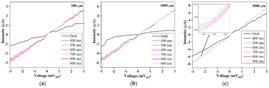
Figure 7.
I(VDS) of the graphene/IDE devices in the dark and under light with different wavelengths (400 to 900 nm). (a) 100 µm; (b) 1000 µm; and (c) 3000 µm. The inset shows a zoom of the curves obtained under continuous illumination.
The responsivity, Rλ, is defined as the ratio of the photocurrent, Iph, or photovoltage, Vph, over the incident light power density (i.e., light power per active area), Pin, as expressed by Equation (1) [28,69,70].
This parameter is often used to evaluate the photodetector’s ability to generate a photocurrent or a photovoltage after illumination. Figure 8 shows the bias-dependent photoresponsivity, Rλ, of all devices at the powers listed in Table S1. The sensitivity is measured at VDS swept from −3 to 3 mV for VG = 0 V. A linear relationship between the source–drain bias and the detector photoresponsivities can be seen. In fact, photoresponsivity increases monotonically as the applied voltage increases. The voltage dependence of the photodetector’s responsivity might be due to the influence of the applied bias on the produced photocurrent. The maximum external photoresponsivity is estimated to be at a bias of −3 mV for all devices. The photoresponsivity decreases when increasing the device size; this may be due to an increase in the resistance of the conduction line. At zero bias, the extracted photoresponsivity is non-zero for the three devices, which may be due to the internal potential created by the asymmetric structure of these devices (R400nm = 2.028 A/W for 100 µm; R400nm = 0.695 A/W for 1000 µm; and R400nm = 0.007 A/W for 3000 µm).
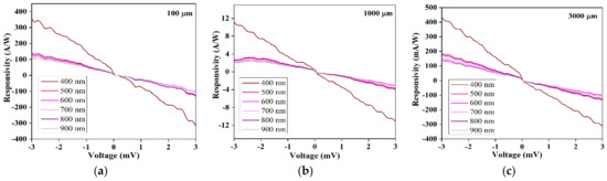
Figure 8.
Responsivity, Rλ (V), of graphene/IDE devices as a function of the wavelength (400 to 900 nm). (a) 100 µm; (b) 1000 µm; and (c) 3000 µm.
Figure 9 shows the variation of responsivity with the wavelength. Due to the resonant nature of the plasmonic design, the sensitivity (photocurrent divided by total power incident on the sample) exhibits a strong wavelength dependence for the same device design. The higher value of Rλ is recorded at 400 nm for all devices.
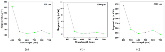
Figure 9.
Responsivity Rλ (λ) of graphene/IDE devices as a function of the wavelength (400 to 900 nm). (a) 100 µm; (b) 1000 µm; and (c) 3000 µm.
The high responsivity of all photodetectors can have several origins. Incident light is tightly concentrated in the region between the different fingers [44]. This can significantly enhance the light–graphene interaction and bypass the short carriers’ lifetime in the graphene layer. This is achieved by collecting all generated photocarriers in the region within the source and the drain, thanks to the size of the fingers nanogap (100 nm) [34,46]. The high photoresponsivity of the graphene photodetector may be a result of the photogating effect. This phenomenon is mainly attributed to the generation of photocarriers in the p-type Si substrate [71,72].
The higher photocurrent can be explained by the high difference between the work functions of the source and the drain (ΔEeff = 0.59 eV) compared to the work of Yoo et al. [34] (ΔEeff = 0.34 eV), which leads to a good separation of photocarriers. The bonding of the graphene layer to Pt and Au surfaces is so weak (≤0.04 eV per carbon atom) that its electronic band structure is preserved and does not undergo strong modification. As schematically shown in Figure 10, the difference in the work functions of graphene (WG = 4.5 eV), Au (WAu = 5.54 eV), and Pt (WPt = 6.13 eV) metals induces doping of the graphene layer, resulting in charge transfer at the contact interface up to the equilibrium of Fermi levels, EF [73,74,75]. Depending on the metal, different types and doping levels can be achieved [34,73,76,77]. As a result, Pt (ΦG = 4.87 eV) shifts the Fermi energy by approximately ΔEF = 370 meV, while Au (ΦG = 4.74 eV) shifts about ΔEF = 240 meV [74]. These values confirm that Pt and Au contacts induce p-type doping of the graphene layer. Therefore, an asymmetric metal arrangement provides additional benefits in enhancing the photovoltaic effect. Indeed, in some cases, the defects can effectively behave as dopants, thus increasing the carriers’ concentration. The defect induces mid-gap states that create a region exhibiting metallic behavior around the vacancy defects.
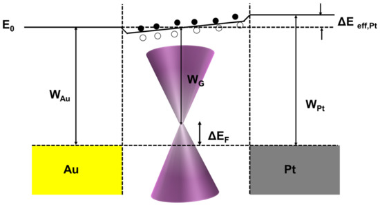
Figure 10.
Schematic diagram of the Au/graphene/Pt band structure. WAu: Au work function, and WPt: Pt work function. E0 is the vacuum level, and ΔEF represents the doping state of the graphene channel. The black-filled (empty) circle is an electron (hole) generated by light absorption.
Table 1 compares key parameters of graphene-based photodetectors found in other published works with the herein-obtained results. Yoo et al. [34] and Sevak Singh et al. [32] have proposed graphene photodetectors with asymmetric contact, which can operate without external voltage. The graphene/silicon photoconductor developed by Gao et al. [78] has a higher responsivity than that of Chen et al. [79], which can be explained by the small gap between the electrodes (200 nm). The highest responsivity reported by Chen et al., at 632 nm, might be due to the mechanism of electron/hole pair separation in the Schottky junction, and to the high carrier mobility in graphene. Graphene-antennas structured with a nanogap (40 nm), proposed by Ye et al. [54], can improve light-absorbing and photocarriers collection. However, their responsivity is still below 1 A W−1. The herein-obtained devices deliver a higher responsivity in a broad spectrum, extending from the visible range to the infrared region (900 nm), making them very competitive in terms of light sensitivity.

Table 1.
Comparison of the obtained photodetector’s parameters with typical graphene photodetectors.
4. Conclusions
A CVD-graphene-based photodetector with asymmetric bottom-side interdigitated gold-platinum (Au-Pt) contacts with a spacing of 100 nm was proposed. The device fabrication process began with the deposition of five metals, Cr/Au/Ta/Pt/Al2O3, by physical vapor deposition (PVD). Due to the high density of the pattern, dose tests were performed to optimize the fabrication of metal contacts. SEM images have confirmed that 583 µC cm−2 was the appropriate dose to obtain the suitable electrode width and spacing. Three IDEs devices with different dimensions (100, 1000, and 3000 µm) were fabricated. A CVD graphene monolayer, confirmed by Raman characterization, was transferred to the top of the IDEs to get a metal-graphene-metal structure. To compare the performance of the three fabricated photodetectors, I(V) characteristics were performed. As the dimension sizes of the devices decreased, the performance of the photodetectors increased to reach R400nm = 358 A/W for a 100 µm device size. Such results were achieved thanks to the high work function difference between the Au and Pt (≈0.59 eV) electrodes, small fingers spacing, and the asymmetric interdigitated structure.
Supplementary Materials
The following supporting information can be downloaded at: https://www.mdpi.com/article/10.3390/chemosensors11030181/s1. Figure S1. Illustration of the devices’ design using LibreCAD software, including (a) the overview of all devices, (b) zoom on 100 µm device, and (c) zoom on the IDEs (Au-Pt); Figure S2. Optical images of devices (a) before and (b) after ion milling; Figure S3. Optical images of devices; Figure S4. Raman mapping of (a) the G and (b) 2D bands positions; Table S1: Power of light used in the photoresponsivity measurement.
Author Contributions
Conceptualization, R.E. and A.B.; formal analysis, R.E. and J.B.; investigation, R.E., J.B. and A.B.; writing—original draft preparation, R.E.; writing—review and editing, R.E., A.B., D.M.F.S. and J.B.; supervision, A.B., J.B., P.A., N.S. and R.C. All authors have read and agreed to the published version of the manuscript.
Funding
Fundação para a Ciência e a Tecnologia (FCT, Portugal) is acknowledged for funding a research contract in the scope of programmatic funding UIDP/04540/2020 (D.M.F.S.).
Data Availability Statement
The authors confirm that all relevant data generated during this study are included in this published article.
Acknowledgments
Rabiaa Elkarous acknowledges the Tunisian Ministry of Higher Education and Scientific Research as well as the University of Tunis El Manar. Rabiaa Elkarous thanks F. Maria Cerqueira for her help with the Raman measurements (INL-International Iberian Nanotechnology Laboratory, Braga, Portugal).
Conflicts of Interest
The authors declare no conflict of interest.
References
- Geim, A.; Novoselov, K. The rise of graphene. Nat. Mater. 2007, 6, 183–191. [Google Scholar] [CrossRef]
- Neto, A.C.; Guinea, F.; Peres, N.; Novoselov, K.; Geim, A. The electronic properties of graphene. Rev. Mod. Phys. 2009, 81, 109–162. [Google Scholar] [CrossRef]
- Novoselov, K.; Geim, A.; Morozov, S.; Jiang, D.-E.; Zhang, Y.; Dubonos, S.; Grigorieva, I.; Firsov, A. Electric field effect in atomically thin carbon films. Science 2004, 306, 666–669. [Google Scholar] [CrossRef]
- Gao, K.; Ran, S.; Han, Q.; Yang, Q.; Jiang, H.; Fu, J.; Leng, C.; Feng, S.; Zhou, D.; Li, Z.; et al. High zero-bias responsivity induced by photogating effect in asymmetric device structure. Opt. Mater. 2022, 124, 112013. [Google Scholar] [CrossRef]
- Brida, D.; Tomadin, A.; Manzoni, C.; Kim, Y.; Lombardo, A.; Milana, S.; Nair, R.; Novoselov, K.; Ferrari, A.; Cerullo, G. Ultrafast collinear scattering and carrier multiplication in graphene. Nat. Commun. 2013, 4, 1987. [Google Scholar] [CrossRef] [PubMed]
- Dawlaty, J.; Shivaraman, S.; Chandrashekhar, M.; Rana, F.; Spencer, M. Measurement of ultrafast carrier dynamics in epitaxial graphene. Appl. Phys. Lett. 2008, 92, 042116. [Google Scholar] [CrossRef]
- Novoselov, K.; Geim, A.; Morozov, S.; Jiang, D.; Katsnelson, M.; Grigorieva, I.; Dubonos, S.; Firsov, A.A. Two-dimensional gas of massless Dirac fermions in graphene. Nature 2005, 438, 197–200. [Google Scholar] [CrossRef] [PubMed]
- Nair, R.; Blake, P.; Grigorenko, A.; Novoselov, K.; Booth, T.; Stauber, T.; Peres, N.; Geim, A. Fine structure constant defines visual transparency of graphene. Science 2008, 320, 1308. [Google Scholar] [CrossRef] [PubMed]
- Kuzmenko, A.; Van Heumen, E.; Carbone, F.; Van Der Marel, D. Universal optical conductance of graphite. Phys. Rev. Lett. 2008, 100, 117401. [Google Scholar] [CrossRef]
- Akinwande, D.; Petrone, N.; Hone, J. Two-dimensional flexible nanoelectronics. Nat. Commun. 2014, 5, 5678. [Google Scholar] [CrossRef]
- Qiu, Q.; Huang, Z. Photodetectors of 2D Materials from Ultraviolet to Terahertz Waves. Adv. Mater. 2021, 33, 2008126. [Google Scholar] [CrossRef] [PubMed]
- Li, Z.; Henriksen, E.; Jiang, Z.; Hao, Z.; Martin, M.; Kim, P.; Stormer, H.; Basov, D. Dirac charge dynamics in graphene by infrared spectroscopy. Nat. Phys. 2008, 4, 532–535. [Google Scholar] [CrossRef]
- Bonaccorso, F.; Sun, Z.; Hasan, T.; Ferrari, A. Graphene photonics and optoelectronics. Nat. Photonics 2010, 4, 611–622. [Google Scholar] [CrossRef]
- Larki, F.; Abdi, Y.; Kameli, P.; Salamati, H. An Effort Towards Full Graphene Photodetectors. Photonic Sens. 2022, 12, 31–67. [Google Scholar] [CrossRef]
- Koppens, F.; Mueller, T.; Avouris, P.; Ferrari, A.; Vitiello, M.; Polini, M. Photodetectors based on graphene, other two-dimensional materials and hybrid systems. Nat. Nanotechnol. 2014, 9, 780–793. [Google Scholar] [CrossRef]
- Yan, Z.; Yang, H.; Yang, Z.; Ji, C.; Zhang, G.; Tu, Y.; Du, G.; Cai, S.; Lin, S. Emerging Two-Dimensional Tellurene and Tellurides for Broadband Photodetectors. Small 2022, 18, 2200016. [Google Scholar] [CrossRef]
- Yu, W.; Gong, K.; Li, Y.; Ding, B.; Li, L.; Xu, Y.; Wang, R.; Li, L.; Zhang, G.; Lin, S. Flexible 2D materials beyond graphene: Synthesis, properties, and applications. Small 2022, 18, 2105383. [Google Scholar] [CrossRef]
- Mu, H.; Yu, W.; Yuan, J.; Lin, S.; Zhang, G. Interface and surface engineering of black phosphorus: A review for optoelectronic and photonic applications. Mater. Futures 2022, 1, 012301. [Google Scholar] [CrossRef]
- Urich, A.; Unterrainer, K.; Mueller, T. Intrinsic Response Time of Graphene Photodetectors. Nano Lett. 2011, 11, 2804–2808. [Google Scholar] [CrossRef]
- George, P.; Strait, J.; Dawlaty, J.; Shivaraman, S.; Chandrashekhar, M.; Rana, F.; Spencer, M. Ultrafast optical-pump terahertz-probe spectroscopy of the carrier relaxation and recombination dynamics in epitaxial graphene. Nano Lett. 2008, 8, 4248–4251. [Google Scholar] [CrossRef]
- Rana, F.; George, P.; Strait, J.; Dawlaty, J.; Shivaraman, S.; Chandrashekhar, M.; Spencer, M. Carrier recombination and generation rates for intravalley and intervalley phonon scattering in graphene. Phys. Rev. B 2009, 79, 115447. [Google Scholar] [CrossRef]
- Park, J.; Ahn, Y.; Ruiz-Vargas, C. Imaging of photocurrent generation and collection in single-layer graphene. Nano Lett. 2009, 9, 1742–1746. [Google Scholar] [CrossRef] [PubMed]
- Freitag, M.; Low, T.; Xia, F.; Avouris, P. Photoconductivity of biased graphene. Nat. Photonics 2013, 7, 53–59. [Google Scholar] [CrossRef]
- Pelella, A.; Grillo, A.; Faella, E.; Luongo, G.; Askari, M.; Di Bartolomeo, A. Graphene–Silicon Device for Visible and Infrared Photodetection. ACS Appl. Mater. Interfaces 2021, 13, 47895–47903. [Google Scholar] [CrossRef]
- Bartolomeo, A.; Luongo, G.; Iemmo, L.; Urban, F.; Giubileo, F. Graphene–Silicon Schottky Diodes for Photodetection. IEEE Trans. Nanotechnol. 2018, 17, 1133–1137. [Google Scholar] [CrossRef]
- Fang, H.; Hu, W. Photogating in low dimensional photodetectors. Adv. Sci. 2017, 4, 1700323. [Google Scholar] [CrossRef]
- Hu, A.-Q.; Liu, Q.-L.; Guo, X. Carrier localization enhanced high responsivity in graphene/semiconductor photodetectors. Chip 2022, 1, 100006. [Google Scholar] [CrossRef]
- Wu, H.; Ding, J.; Yang, D.; Li, J.; Shi, Y.; Zhou, Y. Graphene quantum dots doped ZnO superstructure (ZnO superstructure/GQDs) for weak UV intensity photodetector application. Ceram. Int. 2020, 46, 17800–17808. [Google Scholar] [CrossRef]
- Dawlaty, J.; Shivaraman, S.; Strait, J.; George, P.; Chandrashekhar, M.; Rana, F.; Spencer, M.; Veksler, D.; Chen, Y. Measurement of the optical absorption spectra of epitaxial graphene from terahertz to visible. Appl. Phys. Lett. 2008, 93, 131905. [Google Scholar] [CrossRef]
- Wang, F.; Dukovic, G.; Brus, L.; Heinz, T. Time-Resolved Fluorescence of Carbon Nanotubes and Its Implication for Radiative Lifetimes. Phys. Rev. Lett. 2004, 92, 177401. [Google Scholar] [CrossRef] [PubMed]
- Mueller, T.; Xia, F.; Avouris, P. Graphene photodetectors for high-speed optical communications. Nat. Photonics 2010, 4, 297–301. [Google Scholar] [CrossRef]
- Zhu, W.; Yang, S.; Zheng, H.; Zhan, Y.; Li, D.; Cen, G.; Tang, J.; Lu, H.; Zhang, J.; Zhao, Z.; et al. Gold Enhanced Graphene-Based Photodetector on Optical Fiber with Ultrasensitivity over Near-Infrared Bands. Nanomaterials 2022, 12, 124. [Google Scholar] [CrossRef] [PubMed]
- Lee, S.; Tang, M. Asymmetric interdigitated electrodes for amperometric detection of soluble products. J. Electrochem. Soc. 2021, 168, 057519. [Google Scholar] [CrossRef]
- Yoo, T.; Kim, Y.; Lee, S.; Kang, C.; Chang, K.; Hwang, H.; Revannath, N.; Lee, B. Zero-Bias Operation of CVD Graphene Photodetector with Asymmetric Metal Contacts. ACS Photonics 2018, 5, 365–370. [Google Scholar] [CrossRef]
- Guo, R.; Liu, W.; Zhang, Y.; Hou, Z.; He, C.; Li, J. Multi-channels electrode parallel structure graphene photodetector with high performance. Mater. Lett. 2020, 260, 126948. [Google Scholar] [CrossRef]
- Singh, R.S.; Nalla, V.; Chen, W.; Ji, W.; Wee, A. Photoresponse in epitaxial graphene with asymmetric metal contacts. Appl. Phys. Lett. 2012, 100, 093116. [Google Scholar] [CrossRef]
- Shimomura, K.; Imai, K.; Nakagawa, K.; Kawai, A.; Hashimoto, K.; Ideguchi, T.; Maki, H. Graphene photodetectors with asymmetric device structures on silicon chips. Carbon Trends 2021, 5, 100100. [Google Scholar] [CrossRef]
- Qiao, H.; Huang, Z.; Ren, X.; Liu, S.; Zhang, Y.; Qi, X.; Zhang, H. Self-powered photodetectors based on 2D materials. Adv. Opt. Mater. 2020, 8, 1900765. [Google Scholar] [CrossRef]
- Tian, W.; Wang, Y.; Chen, L.; Li, L. Self-Powered Nanoscale Photodetectors. Small 2017, 13, 1701848. [Google Scholar] [CrossRef]
- Cha, J.; Son, J.; Hong, J. A Bottom-Electrode Contact: The Most Suitable Structure for Graphene Electronics. Adv. Mater. Interfaces 2020, 9, 2102207. [Google Scholar] [CrossRef]
- Bharadwaj, B.K.; Nath, D.; Pratap, R.; Raghavan, S. Making consistent contacts to graphene: Effect of architecture and growth induced defects. Nanotechnology 2016, 27, 205705. [Google Scholar] [CrossRef] [PubMed]
- Zarei, M.; Sharifi, M. Graphene nanoribbon photodetectors based on an asymmetric potential barrier: A new concept and a new structure. J. Comput. Electron. 2018, 17, 531–539. [Google Scholar] [CrossRef]
- Mueller, T.; Xia, F.; Freitag, M.; Tsang, J.; Avouris, P. Role of contacts in graphene transistors: A scanning photocurrent study. Phys. Rev. B 2009, 79, 245430. [Google Scholar] [CrossRef]
- Yao, Y.; Kats, M.; Genevet, P.; Yu, N.; Song, Y.; Kong, J.; Capasso, F. Broad electrical tuning of graphene-loaded plasmonic antennas. Nano Lett. 2013, 13, 1257–1264. [Google Scholar] [CrossRef]
- Chakraborty, C.; Beams, R.; Goodfellow, K.; Wicks, G.; Novotny, L.; Vamivakas, A. Optical antenna enhanced graphene photodetector. Appl. Phys. Lett. 2014, 105, 241114. [Google Scholar] [CrossRef]
- Cusati, T.; Fiori, G.; Gahoi, A.; Passi, V.; Lemme, M.; Fortunelli, A.; Iannaccone, G. Electrical properties of graphene-metal contacts. Sci. Rep. 2017, 7, 5109. [Google Scholar] [CrossRef]
- Zhu, Y.; Murali, S.; Cai, W.; Li, X.; Suk, J.; Potts, J.; Ruoff, R. Graphene and graphene oxide: Synthesis, properties, and applications. Adv. Mater. 2010, 22, 3906–3924. [Google Scholar] [CrossRef]
- Chen, Y.; Gong, X.; Gai, J. Progress and challenges in transfer of large-area graphene films. Adv. Sci. 2016, 3, 1500343. [Google Scholar] [CrossRef]
- Kobayashi, T.; Bando, M.; Kimura, N.; Shimizu, K.; Kadono, K.; Umezu, N.; Miyahara, K.; Hayazaki, S.; Nagai, S.; Mizuguchi, Y. Production of a 100-m-long high-quality graphene transparent conductive film by roll-to-roll chemical vapor deposition and transfer process. Appl. Phys. Lett. 2013, 102, 023112. [Google Scholar] [CrossRef]
- Ahn, Y.; Kim, H.; Kim, Y.-H.; Yi, Y.; Kim, S.-I. Procedure of removing polymer residues and its influences on electronic and structural characteristics of graphene. Appl. Phys. Lett. 2013, 102, 091602. [Google Scholar] [CrossRef]
- Suk, J.; Lee, W.; Lee, J.; Chou, H.; Piner, R.; Hao, Y.; Akinwande, D.; Ruoff, R. Enhancement of the electrical properties of graphene grown by chemical vapor deposition via controlling the effects of polymer residue. Nano Lett. 2013, 13, 1462–1467. [Google Scholar] [CrossRef] [PubMed]
- Ullah, S.; Yang, X.; Ta, H.; Hasan, M.; Bachmatiuk, A.; Tokarska, K.; Trzebicka, B.; Fu, L.; Rummeli, M. Graphene transfer methods: A review. Nano Res. 2021, 14, 3756–3772. [Google Scholar] [CrossRef]
- Liao, C.-D.; Capasso, A.; Queirós, T.; Domingues, T.; Cerqueira, F.; Nicoara, N.; Borme, J.; Freitas, P.; Alpuim, P. Optimizing PMMA solutions to suppress contamination in the transfer of CVD graphene for batch production. Beilstein J. Nanotechnol. 2022, 13, 796–806. [Google Scholar] [CrossRef] [PubMed]
- Ye, M.; Gao, Y.; Cadusch, J.; Balendhran, S.; Crozier, K. Mid-Wave Infrared Polarization-Independent Graphene Photoconductor with Integrated Plasmonic Nanoantennas Operating at Room Temperature. Adv. Opt. Mater. 2021, 9, 2001854. [Google Scholar] [CrossRef]
- Gangnaik, A.; Georgiev, Y.; Holmes, J. New Generation Electron Beam Resists: A Review. Chem. Mater. 2017, 29, 1898–1917. [Google Scholar] [CrossRef]
- Hasan, R.; Luo, X. Promising Lithography Techniques for Next-Generation Logic Devices. Nanomanufact. Metrol. 2018, 1, 67–81. [Google Scholar] [CrossRef]
- Ferrari, A.; Meyer, J.; Scardaci, V.; Casiraghi, C.; Lazzeri, M.; Mauri, F.; Piscanec, S.; Jiang, D.; Novoselov, K.; Roth, S. Raman spectrum of graphene and graphene layers. Phys. Rev. Lett. 2006, 97, 187401. [Google Scholar] [CrossRef]
- Malard, L.; Pimenta, M.; Dresselhaus, G.; Dresselhaus, M. Raman spectroscopy in graphene. Phys. Rep. 2009, 473, 51–87. [Google Scholar] [CrossRef]
- Wu, J.-B.; Lin, M.-L.; Cong, X.; Liu, H.-N.; Tan, P.-H. Raman spectroscopy of graphene-based materials and its applications in related devices. Chem. Soc. Rev. 2018, 47, 1822–1873. [Google Scholar] [CrossRef]
- Ferrari, A.; Robertson, J. Resonant Raman spectroscopy of disordered, amorphous, and diamondlike carbon. Phys. Rev. B 2001, 64, 075414. [Google Scholar] [CrossRef]
- Thomsen, C.; Reich, S. Double Resonant Raman Scattering in Graphite. Phys. Rev. Lett. 2000, 85, 5214–5217. [Google Scholar] [CrossRef] [PubMed]
- Hao, Y.; Wang, Y.; Wang, L.; Ni, Z.; Wang, Z.; Wang, R.; Koo, C.; Shen, Z.; Thong, J. Probing layer number and stacking order of few-layer graphene by Raman Spectroscopy. Small 2010, 6, 195–200. [Google Scholar] [CrossRef] [PubMed]
- Das, A.; Chakraborty, B.; Sood, A. Raman spectroscopy of graphene on different substrates and influence of defects. Bull. Mater. Sci. 2008, 31, 579–584. [Google Scholar] [CrossRef]
- Casiraghi, C.; Pisana, S.; Novoselov, K.; Geim, A.; Ferrari, A. Raman fingerprint of charged impurities in graphene. Appl. Phys. Lett. 2007, 91, 233108. [Google Scholar] [CrossRef]
- Casiraghi, C. Probing disorder and charged impurities in graphene by Raman spectroscopy. Phys. Status Solidi (RRL) Rapid Res. Lett. 2009, 3, 175–177. [Google Scholar] [CrossRef]
- Liu, Y.; Tan, Z.; Kumar, M.; Abhilash, T.; Liu, G.-J.; Hakonen, P. Defects in h-BN tunnel barrier for local electrostatic probing of two dimensional materials. APL Mater. 2018, 6, 091102. [Google Scholar] [CrossRef]
- Hanna, A.; Tinkham, M. Variation of the Coulomb staircase in a two-junction system by fractional electron charge. Phys. Rev. B 1991, 44, 5919–5922. [Google Scholar] [CrossRef]
- Mullen, K.; Ben-Jacob, E.; Jaklevic, R.; Schuss, Z. I-Vcharacteristics of coupled ultrasmall-capacitance normal tunnel junctions. Phys. Rev. B 1988, 37, 98–105. [Google Scholar] [CrossRef]
- Geng, H.; Yuan, D.; Yang, Z.; Tang, Z.; Zhang, X.; Yang, K.; Su, Y. Graphene van der Waals heterostructures for high-performance photodetectors. J. Mater. Chem. C 2019, 7, 11056–11067. [Google Scholar] [CrossRef]
- Zhu, X.; Xie, Q.; Tian, H.; Zhang, M.; Gou, Z.; He, S.; Gu, P.; Wu, H.; Li, J.; Yang, D. High photoresponse sensitivity of lithium-doped ZnO (LZO) thin films for weak ultraviolet signal photodetector. J. Alloys Compd. 2019, 805, 309–317. [Google Scholar] [CrossRef]
- Ogawa, S.; Shimatani, M.; Fukushima, S.; Okuda, S.; Kanai, Y.; Ono, T.; Matsumoto, K. Broadband photoresponse of graphene photodetector from visible to long-wavelength infrared wavelengths. Opt. Eng. 2019, 58, 057106. [Google Scholar]
- Fukushima, S.; Shimatani, M.; Okuda, S.; Ogawa, S.; Kanai, Y.; Ono, T.; Inoue, K.; Matsumoto, K. High-Responsivity Graphene Infrared Photodetectors Using Photo-Gating Effect, Infrared Technology and Applications XLV; SPIE: Paris, France, 2019; pp. 450–455. [Google Scholar]
- Giovannetti, G.; Khomyakov, P.; Brocks, G.; Karpan, V.; van den Brink, J.; Kelly, P. Doping Graphene with Metal Contacts. Phys. Rev. Lett. 2008, 101, 026803. [Google Scholar] [CrossRef] [PubMed]
- Khomyakov, P.; Giovannetti, G.; Rusu, P.; Brocks, G.; van den Brink, J.; Kelly, P. First-principles study of the interaction and charge transfer between graphene and metals. Phys. Rev. B 2009, 79, 195425. [Google Scholar] [CrossRef]
- Ruffino, F.; Meli, G.; Grimaldi, M. Nanoscale electrical characteristics of metal (Au, Pd)–graphene–metal (Cu) contacts. Solid State Commun. 2016, 225, 1–6. [Google Scholar] [CrossRef]
- Lee, E.; Balasubramanian, K.; Weitz, R.; Burghard, M.; Kern, K. Contact and edge effects in graphene devices. Nat. Nanotechnol. 2008, 3, 486–490. [Google Scholar] [CrossRef] [PubMed]
- Gan, X.; Shiue, R.-J.; Gao, Y.; Meric, I.; Heinz, T.; Shepard, K.; Hone, J.; Assefa, S.; Englund, D. Chip-integrated ultrafast graphene photodetector with high responsivity. Nat. Photonics 2013, 7, 883–887. [Google Scholar] [CrossRef]
- Gao, Y.; Tao, L.; Tsang, H.; Shu, C. Graphene-on-silicon nitride waveguide photodetector with interdigital contacts. Appl. Phys. Lett. 2018, 112, 211107. [Google Scholar] [CrossRef]
- Chen, Z.; Cheng, Z.; Wang, J.; Wan, X.; Shu, C.; Tsang, H.; Ho, H.; Xu, J. High responsivity, broadband, and fast graphene/silicon photodetector in photoconductor mode. Adv. Opt. Mater. 2015, 3, 1207–1214. [Google Scholar] [CrossRef]
- Ostovari, F.; Moravvej-Farshi, M. Photodetectors with zigzag and armchair graphene nanoribbon channels and asymmetric source and drain contacts: Detectors for visible and solar blind applications. J. Appl. Phys. 2016, 120, 144505. [Google Scholar] [CrossRef]
- Selamneni, V.; Mukherjee, A.; Raghavan, H.; Gomathi, P.; Kolli, C.; Pal, S.; Hazra, A.; Sahatiya, P. Plasmonic Au Nanoparticles Coated on ReS2 Nanosheets for Visible-Near-Infrared Photodetectors. ACS Appl. Nano Mater. 2020, 5, 11381–11390. [Google Scholar] [CrossRef]
- Li, J.; Nie, C.; Sun, F.; Tang, L.; Zhang, Z.; Zhang, J.; Zhao, Y.; Shen, J.; Feng, S.; Shi, H.; et al. Enhancement of the Photoresponse of Monolayer MoS2 Photodetectors Induced by a Nanoparticle Grating. ACS Appl. Mater. Interfaces 2020, 12, 8429–8436. [Google Scholar] [CrossRef] [PubMed]


Disclaimer/Publisher’s Note: The statements, opinions and data contained in all publications are solely those of the individual author(s) and contributor(s) and not of MDPI and/or the editor(s). MDPI and/or the editor(s) disclaim responsibility for any injury to people or property resulting from any ideas, methods, instructions or products referred to in the content. |
© 2023 by the authors. Licensee MDPI, Basel, Switzerland. This article is an open access article distributed under the terms and conditions of the Creative Commons Attribution (CC BY) license (https://creativecommons.org/licenses/by/4.0/).