Abstract
In this review article, the state of the art of the complete processing chain in the production of solar photo-electric modules from raw materials (quartzites, quartz sand) is detailed. In particular, the silicon and silane production technologies of the Institute of Physics and Technology of Almaty, Kazakhstan, can become part of an expansive technologies chain. Such integration could present a number of benefits in comparison with the analogs, including less environmental pressure and increased safety. The combination of innovative production technologies of highly effective solar cells and modules with competitive production technologies of solar-grade silicon and silane constitutes a basis for the creation of an industrial cluster in the field of silicon solar photo energy with a complete vertically integrated production cycle.
1. Introduction
The energy sector, traditionally slow-changing, has been experiencing unprecedented growth in recent years. This is largely due to the emergence of renewable energy sources. Meanwhile, political priorities such as climate change, energy security, and air pollution have made the transition to renewable energy a priority for the world community. Today, we are entering a new era in which transformation in the energy sector will drive the transformation of the economic sector, as the transition to a low-carbon energy sector remains a key to climate neutrality. Today, the share of greenhouse gas emissions from traditional energy-producing industries is more than two-thirds of total greenhouse gas emissions [1].
The rapid development of renewable energy sources and their increasing importance in the worldwide energy balance are the latest trends. One of the most dynamic commercial renewable energy sources is solar photovoltaics [2]. Solar energy has a number of advantages over alternative energy sources: it is widely available and inexhaustible, the conversion of light into electricity does not directly influence the environment, and solar installations are modular, enabling the construction of electricity generation systems of any required size and power and the ability to operate solar installations both on-grid and off-grid.
The main electricity-generating component of solar modules is a solar cell made of materials directly converting solar radiation into electricity. Currently, commercial solar cells can be divided into the following groups:
- Wafer-based crystalline Si solar cells (made of monocrystalline Si, multi-crystalline Si, polycrystalline Si)—occupying 85–90% of the market; and
- Thin-film solar cells (made of amorphous Si, CdTe, CuInGaSe2 (CIGS) or CuInSe2 (CIS), GaAs/Ge, organic materials and organohalide perovskites)—occupying around 15–20% of the market.
The market share of crystalline silicon solar cells has appeared to grow over time in recent years. Silicon is the second most abundant element in the Earth’s crust, constituting 26% of its mass, and is generally safe for the environment. Due to these factors and taking into account the ever-decreasing prices of silicon solar modules, it is difficult to imagine another material being able to replace it in the near and even distant future [3].
The Institute of Physics and Technology (Almaty, Kazakhstan) has several works about methods of metallurgical-grade silicon (MG-Si) production and purification of silicon to upgraded metallurgical-grade silicon (UMG-Si) and works about silane production methods. As a result of conducted studies and works, purified silicon samples and Si crystals grown by the Czochralski method were obtained on a laboratory scale, approximately 2–3 kg; the results are summarized in [4]. Based on the results of the previous study, the process of integrating silicon production technology on an industrial scale was planned within the framework of the KazPV project. The KazPV Project is aimed at “Creating of the production of photovoltaic modules based on Kazakhstan silicon”, which includes the production of MG-Si and solar-grade silicon (SoG-Si), solar cells, and photovoltaic modules. The first solar-grade silicon was obtained and test solar cells were created under KazPV project [5,6,7,8]. This initiative has not been completed yet, and it is planned to continue work in both directions, namely, silicon purification and growing Si ingots and producing solar cell.
This article mainly focuses on the analysis of technological processes employed in the production of silicon solar cells and modules and the identification of some of the most promising threads, from the authors’ viewpoint, for further development of large-scale terrestrial solar photovoltaics.
2. Silicon Classification
Silicon raw materials are divided into the following grades by impurity concentration (see Table 1):

Table 1.
Concentrations of impurities in various grades of silicon.
- Metallurgical-grade silicon (MG-Si) is usually produced by carbothermic preparation. MG-Si is used in the iron and steel industry as the doping material and is the raw material for solar- and electrical-grade silicon.
- Solar-grade silicon (SoG-Si) is derived from MG-Si by its further purification and intended for use in SC.
- Electronic-grade silicon (EG-Si) used for the production of solid-state electronic devices, chips, etc.
3. Metallurgical-Grade Silicon
The most common method for producing MG-Si is the reduction of quartzite with carbon (carbothermal process) in an arc furnace with immersed electrodes. Impurity levels in MG-Si are of decisive importance for the purity of the starting quartzites and the carbonaceous reducing agents used in the carbothermal process. High-purity quartz concentrates are obtained by grinding natural quartz to a size of 100–300 microns, which are further purified from mineral and chemical impurities. To specify the purity of high-purity quartz concentrates, IOTA classification is used. It is Unimin (USA) quartz concentrate-grade classification. IOTA is characterized by low concentrations of Al, Fe, and alkaline earth metals. Minimum and maximum concentrations of impurities in quartzite, the most often used for solar energy, are as follows: 25 ppm > Al > 10–12 ppm; Fe ˂ 1 ppm; alkaline earth ˂ 7–12 ppm [9].
One of the promising approaches to metallurgical silicon production is aluminothermal technology (Figure 1). Raw materials for it are quartz raw materials and technical aluminum. This technology demonstrates its feedstock tolerance, allowing one to work with both large pieces of quartzite and bulk feedstock in the form of quartz sand [10,11]. In addition, waste from phosphorus and metallurgical industries can be used as quartz raw materials [12,13]. The main reaction in this technology is:
3SiO2 + 4Al = 3Si + 2Al2O3,
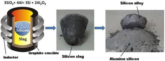
Figure 1.
The process of silicon purification by the aluminothermy method.
The reaction takes place at a temperature of 1200–1300 °C. The main advantages of this technology in comparison with the carbothermal process are the possibility of obtaining cleaner reduction products based on difficult-to-remove boron and phosphorus impurities, high process efficiency in terms of the use of materials and energy, and the production of high-alumina cement as a waste product.
4. Upgraded Metallurgical-Grade Silicon
One of the promising technologies for obtaining silicon that meets the requirements for silicon of “solar quality” is the direct purification of metallurgical silicon to obtain improved metallurgical silicon (upgraded metallurgical-grade silicon—UMG-Si). Work in this area began at the end of the 1980s by Siemens, Solarex, Bayer, Heliotronic (subsidiary of Wacker Chemie), and a number of other American and Japanese companies [14,15,16,17].
The process details may vary from manufacturer to manufacturer, but as a rule, such technologies involve removing metal impurities and reducing the boron and phosphorus content necessary for the production of “solar-grade” silicon. Most of the existing production facilities consist of the following elements:
- Carbothermal reduction of quartz from selected raw materials to minimize the content of impurities; and
- Bucket refining using gas (or plasma) or slag.
The final product purity reaches 99.99% [18]. The first studies on obtaining improved metallurgical silicon were of more scientific than applied importance due to low economic demand for solar modules. In 2004–2008, due to the shortage of high-purity silicon, interest in solar energy was revived, leading to the emergence of new UMG-Si production facilities [19,20,21]. In particular, Q-Sells (Germany) had a long-term contract for the supply of UMG silicon with Elkem (Norway), Solarvalue (Slovenia), and Timminco Ltd. (Canada), and produced solar panels from it with efficiency over 15% [22].
The aluminothermal technology development for processing phosphorus production waste and high-purity Kazakhstani quartzites in the past few years has made it possible to obtain improved metallurgical silicon with a low content of hard-to-remove boron and phosphorus impurities at a level of 1 ppmw [23,24,25]. In this case, the resulting product purity reaches 99.95%, and the yield is 75–85%. Silicon obtained by the aluminothermal treatment method has structure and phase composition that sharply differ from those for conventional metallurgical silicon, and the subsequent acid cleaning has a higher efficiency compared to acid cleaning of conventional commercial metallurgical-grade silicon. Thanks to the developed method of slag cleaning, effective removal of phosphorus and boron is achieved by binding phosphorus with aluminum and subsequent sublimation. Demonstration of aluminothermal technology for UMG-Si production with hard-to-remove boron and phosphorus impurities at the level of solar-grade silicon raises the question whether it is possible to combine this technology with directional crystallization methods that can effectively remove remaining metal impurities with simultaneous growth of crystalline ingots at a low cost.
5. Gaseous Silicon Compounds
The main raw materials for obtaining high-purity silicon of electronic quality are gaseous compounds: trichlorosilane (SiHCl3) and monosilane (SiH4) [26]. Most polycrystalline silicon wafers for the solar industry are obtained with the so-called Siemens method by using trichlorosilane [27,28]. Monosilane technology is an alternative to traditional chloride technology. Union Carbide (USA) first developed this process in the late 1980s. According to this method, the process for monosilane production consists of several stages: silicon tetrachloride hydrogenation in reactors with a fluidized bed at a temperature of about 500 °C and pressure of about 3–4 MPa to obtain chlorosilanes, vapor–gas mixture condensation, purification of chlorosilanes from low-boiling impurities and separation into light ends consisting of trichlorosilane and dichlorosilane, heavy ends consisting of silicon tetrachloride, disproportionation of trichlorosilane and dichlorosilane to obtain monosilane and a mixture of chlorosilanes, purification of monosilane (Figure 2). Then, monosilane materials are exposed to pyrolysis at 800–1000 °C in free space reactors, in fluidized bed reactors, and in rod-type reactors (as in the Siemens method). Polycrystalline silicon (poly-Si) produced by this method features low levels of the most harmful boron, phosphorus, and carbon impurities at./cm3: boron <3 × 10¹²; phosphorus 1.5 × 10¹³; carbon 2.5 × 10¹⁶ [29,30]. For more than 20 years, Union Carbide technology has significantly improved and is used in a modified form by REC (Brockton, MA, USA), the world’s largest monosilane producer.
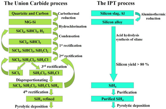
Figure 2.
Process comparison: Union Carbide corporation vs Institute of Physics and Technology (IPT).
An alternative to the Union Carbide method for monosilane preparation is acidolysis of silicon-containing alloys [31,32]. For example, the ternary alloy CaxAlySiz was previously demonstrated, which, when reacted with a mineral acid solution, leads to the release of predominantly monosilane (SiH4) [33,34]. At the beginning of the work, the starting material (ternary alloy powder) is loaded into a dosing device. The reactor and the metering device are sealed and purged with nitrogen to displace oxygen. After that, water is fed into the reactor, and then concentrated hydrochloric acid is supplied through the acid line in the calculated quantity and in established portions. Before the first portion of the acid is fed into the reactor, a stirrer is turned on. The steam–gas mixture (crude silane) leaving the silane synthesis reactor is sent to the refrigerator for drying to remove the main portion of moisture (in the form of hydrochloric acid). The condensate is returned to the silane synthesis reactor, and the raw silane stream is directed to a condenser with the temperature maintained below the silane condensation temperature by using the refrigerator. After filling the condenser with silane, the temperature of the refrigerator is raised stepwise and the silane is fed to the rectification column where higher-boiling impurities are removed from the entire evaporation cube, and then to the column where lower-boiling impurities are removed from the reflux condenser. The silane purified by rectification is accumulated in a condenser with a refrigerator. The purification pattern should make it possible to obtain silane with an impurity concentration that would ensure the production of polysilicon suitable for solar cells. Silane purified according to the developed pattern should ensure the production of polycrystalline silicon rods with a boron purity level of at least 2 × 10¹⁶ at./cm3 (1–2 ohm∙cm, p-type) and with a donor purity level of 2–5.7 × 10¹⁷ at./cm3 (0.1–1 ohm∙cm, n-type) conductivity. Silicon with this level of purity is suitable for solar cell production.
Compared to the traditional monosilane production method, the new technology is expected to offer significant cost savings that will extend to subsequent process steps (see Figure 2).
6. Mono- and Polysilicon Ingots Production
Polycrystalline silicon obtained in the form of rods serves as a raw material for the production of monocrystalline silicon ingots by the Czochralski and zone melting methods [35].
Currently, monocrystalline silicon is manly produced by the Czochralski method (80–90%) [36,37], in which purified polycrystalline silicon is melted in a crucible from highly pure quartz in a high-vacuum furnace. This method is used to grow the largest single crystals.
According to the zone melting method, ingots are grown in vacuum without crucibles. The polycrystalline ingot is fixed in holders and melted using the high-frequency inductor. The molten narrow part moves along the ingot from the bottom up and is held by the forces of surface tension between the liquid and solid zones. The method is based on unequal solubility of impurities in the liquid and solid phases. When the molten zone moves along the length of the ingot, impurities are pushed back to its end. The upper part of the ingot most contaminated with impurities is cut off and sent for remelting. After 15–20 passes, silicon of the desired quality is obtained. The difference from the Czochralski method is that the material obtained after zone melting is not contaminated, since it does not come into contact with the wall [38].
The most polycrystalline silicon intended for photovoltaic industry is obtained by directional crystallization. In this method, silicon to be purified is melted in large square quartz crucibles, followed by directional crystallization of ingots from bottom to top by cooling the bottom of the crucible. The resulting columnar structures in silicon provide a minority carrier lifetime sufficient for use in photovoltaics.
7. Solar Cell Production
After cooling the grown ingots of poly- or monocrystalline silicon, the ingot edges are cut off, thereby removing areas with high impurity concentrations. Crystals obtained are shaped (squared), ground, and cut into plates. Dimensions of crystalline solar cells are usually 125 × 125 mm2 or 156 × 156 mm2. Furthermore, solar cell manufacturers texturize silicon wafers and create semiconductor structures, as a rule, by the high-temperature phosphorus diffusion method, and the application of electrical contacts.
7.1. Amorphous Silicon Solar Cells
Amorphous silicon solar cells are a cheaper alternative to crystalline solar cells. Usually, they are produced on rigid substrates (glass, metal, etc.), but it is also possible to manufacture them on flexible surfaces [39,40]. The starting material in the production of amorphous silicon solar cells is monosilane. The main method of deposition on a substrate is plasma chemical vapor deposition (PECVD). Amorphous silicon is a hydrogenated form of silicon (a-Si:H), since it contains hydrogen in an amount of 5 to 20 at %, and therefore, the amorphous silicon film has stable semiconducting properties.
Advantages of amorphous silicon over crystalline silicon are the possibility and comparative simplicity of making solar cells with a large area (more than 1 m2) at lower deposition temperatures (about 200 °C), as well as specific semiconductor properties that can be controlled to obtain the required specification by selecting the optimal combinations of film components. In addition, solar cells based on amorphous silicon provide a higher solar energy conversion efficiency at elevated temperatures of 40–60 °C and in conditions of high cloud coverage [41,42].
Another important advantage of amorphous silicon is the ability to fabricate multi-junction structures using several layers with different bandgap widths. The most frequently manufactured multijunction amorphous solar cells consist of upper a-Si:H and lower microcrystalline silicon (μc-Si:H) layers [43,44,45]. μc-Si:H is a two-phase material consisting of crystallites (D ˂ 20 nm) embedded in an amorphous silicon matrix [46]. The first solar cell with this structure was manufactured in 1994 at the Institute of Microengineering of the University of Switzerland and demonstrated 4.6% efficiency [47].
There are no technical losses associated with cutting, grinding, and polishing in amorphous silicon solar cell technology, which exist in the monocrystalline silicon-based solar cell manufacturing. This helps to reduce the cost of production processes.
The disadvantage of solar cells based on amorphous silicon is that their efficiency is approximately 2 times lower than that of crystalline silicon cells for a higher defect density and light induction due to the Staebler–Wronski effect [48,49].
In 1976, the first thin-film solar module based on a-Si with 2.4% efficiency was produced at RCA Laboratories [50]. The highest demonstrated efficiency of a single-junction thin-film photocell based on amorphous silicon is 10.1% [39]. In this photocell, amorphous silicon was deposited on ZnO:B substrate by low-pressure chemical vapor deposition (LPCVD). The efficiency is slightly higher than 13.6% in tandem (double) amorphous silicon elements (a-Si/nc-Si/nc-Si) [51,52].
7.2. Silicon Hetero-Junction (HIT) Solar Cells
High efficiency of monocrystalline silicon and low cost of amorphous silicon are successfully combined in a heterojunction solar cell known as HIT (heterostructure with intrinsic thin layer technology). In HIT elements, the basis is monocrystalline silicon with thin layers of amorphous silicon deposited on the surface. The application of two materials with different bandgap widths significantly expands the absorption spectrum of the solar cell, increasing its efficiency. On the industrial scale, the silicon heterojunction technology makes it possible to obtain solar cells with efficiency over 20% [53,54].
Heterojunction silicon solar cell technology was first patented by Sanyo in the early 1990s. The first elements using this technology were based on a heterojunction of n-type crystalline silicon and p-type amorphous silicon. The maximum efficiency for such a solar cell structure has reached 12.3%. The introduction of a thin a-Si:H intrinsic conduction layer between the n-type and p-type silicon layers led to a further increase in solar cell performance. Improving the surface quality in heterojunction elements based on p- and n-type Si wafers showed that a sample using the n-type wafer demonstrates higher efficiency (17.6%) compared to a sample using the p-type wafer. (16.4%) [55,56,57].
A significant part of the incident radiation will be reflected even with the textured crystalline silicon wafer due to the high difference in refractive indices between amorphous silicon (n = 4–5) and air (n = 1). Transparent conducting oxide (TCO) coatings, playing the role of electrodes in HIT cells, have refractive indices ranging from 1 to 5, and can significantly reduce the reflected radiation.
HIT technology currently competes with the traditional technology where the p–n junction is formed by the impurity diffusion method [58,59]. Solar cells made using traditional technology can demonstrate comparable levels of efficiency, but this is usually achieved through complex and energy-intensive technological operations. Table 2 shows a comparison of HIT heterojunction elements with elements having the PERL structure (passivated emitter with local doping of the rear surface).
Table 2.
Comparison of PERL solar cells with heterojunction elements (based on [60,61]).
8. Solar Module Production
After dimensioning and processing both sides of a substrate (grinding, texturing, chemical processing, etc.), the contact grids are applied on future photo cells. Most of producers use a screen-printing method (silk screen process). The method is considered simple as it can be applied on substrates both made of ideal single-crystal and low-quality multicrystal silicon. They use complex silver pastes for the face side, and aluminum and silver for the back side. The face side contact grid consists of several dozens of finger-type current collectors located perpendicularly to 2 or 3 broad contacts. Then, completed solar elements are assembled in modules and the modules are assembled in solar panels. SE in the module can be connected in parallel, in series, or in parallel series. SE are connected with each other by metal tapes (buses). Soldering flux is applied on each element and tapes are soldered. After soldering, the photo cells are cleaned by ultrasound in water at 60 °C. Then, they are dried and several photo cells are soldered in a row. The number of connected SEs in a module is determined by the required rated voltage. Modules with 36 SEs with four rows, each of which consists of nine elements, are standard for most producers. Photo cells are checked with a voltmeter, as it is easy to correct soldering at this stage. A metal tape connecting these rows is applied through ready lines. Then, the system is put face side down on transparent laminated glass. The glass serves as a base supporting the photo cells. The module is sealed with ethylene vinyl acetate (EVA) and polyethyleneterephthalate protective film. The obtained sandwich structure is laminated in a furnace within 15 min for reliable fixing to the protective glass and reflection loss minimization.
The innovative solar cell module connection technology called SmartWire Connection was presented in 2014 at the Intersolar Exhibition in Munich. SmartWire Connection technology uses a wire matrix with more than 2000 points of connection with conducting fingers instead of standard tape connectors for conducting buses. Thin wires made of a foil are coiled on a polymer film. The ends of wires are connected by a wide bus, which serves as a bridge and transmitter for the serial connection of photo cells to the module. The obtained film and wire structure is applied on a photo cell with preliminarily mapped contacts by means of vacuum (see Figure 3). Photo cells are assembled with a semi-automated machine where the desirable module size (36/48/60/72) is set. Connections are made by the same film and wire structure but from the back. Photo cells assembled in a cellular matrix are placed in a vacuum and laminated. The electric connection of photo cell rows occurs during the process of lamination.
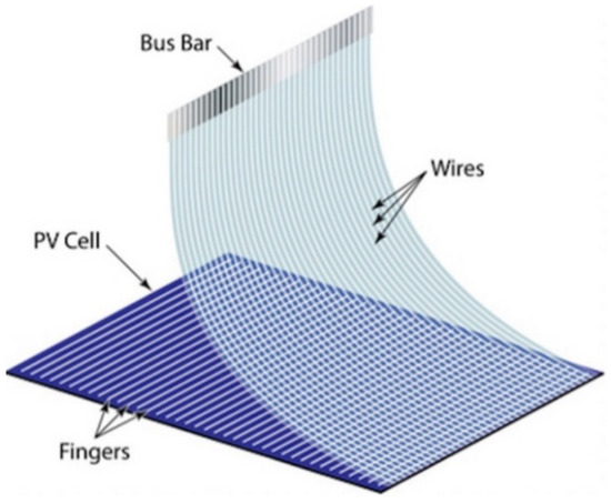
Figure 3.
SmartWire connections applied to the photocell, reprinted from [64].
The main benefits of wire foil application in comparison with SE with connecting tapes [65,66,67,68] include:
- Reduced shading of the face surface thanks to thin wires dozens of micrometers wide;
- Reduced quantity of required silver due to replacement with copper wires by 70%; and
- Up to 10% increased quantity of produced electricity without increasing the module cost.
9. Conclusions
This review work demonstrates the complete production chain of finished goods in the field of solar photo energy from raw materials (quartzites, quartz sand) to the end product (solar photo-electric modules). Along with popular technologies, we describe a number of technologies, particularly the silicon and silane production technologies of the Physics and Technology Institute of Almaty, Kazakhstan, which can become part of the described production chain possessing a number of benefits, including reduced environmental stress and improved safety. On the basis of these technologies, complete vertically integrated solar photo-electric clusters can be established, allowing us to considerably reduce production cost of finished goods in the industry, creating local points of economic growth independent of external market factor effects. It is obvious that in conditions of increasing quantities of hydro carbonic raw materials on international markets, reduced solar quality silicon production cost and less environmental stress from this process are some of the most important arguments for the subsequent growth of solar power’s role in the world energy balance. The combination of innovative production technologies of highly effective solar elements and modules with competitive technologies of solar quality silicon and silane production constitutes a basis for establishing an industrial cluster in the field of silicon solar photo energy with a complete vertically integrated production cycle. This will allow creating conditions for further decreases in the prices of final products and an increased share of renewable energy sources in the worldwide energy balance.
The review article shows that our studies can be integrated with international technologies in order to develop and enhance the entire process chain from silicon to solar cells in Kazakhstan. These major opportunities are beneficial for Kazakhstan, and the technology may also become promising for other countries with further improvement. Moreover, in the event of successful project completion, it is a favorable export item in the long term. Of course, further activities will depend on the government, as such projects are only possible with governmental support.
Author Contributions
A.S. (Abay Serikkanov), writing the manuscript. A.S. (Aigul Shongalova), writing the manuscript. K.Z., writing the manuscript. N.T., writing and revising the manuscript. T.T., writing and revising the manuscript. A.P., writing the manuscript. B.M., leadership of the project. All authors have read and agreed to the published version of the manuscript.
Funding
This research was funded by the Ministry of Education and Science of the Republic of Kazakhstan, grant no. AP08856059.
Conflicts of Interest
The authors declare no conflict of interest.
References
- Gielen, D.; Gorini, R.; Leme, R.; Prakash, G.; Wagner, N.; Janeiro, L.; Collins, S.; Kadir, M.; Asmelash, E.; Ferroukhi, R.; et al. Energy Transitions Outlook: 1.5 °C Pathway; International Renewable Energy Agency: Abu Dhabi, United Arab Emirates, 2021; Available online: http://www.irena.org/publications (accessed on 13 February 2022).
- Ssemombwe, R. Solar Power Production Efficiency. Ph.D. Thesis, Makerere University, Kampala, Uganda, 2021. [Google Scholar]
- Seo, B.; Kim, J.Y.; Chung, J. Overview of global status and challenges for end-of-life crystalline silicon photovoltaic panels: A focus on environmental impacts. Waste Manag. 2021, 128, 45–54. [Google Scholar] [CrossRef] [PubMed]
- Mukashev, B.; Abdullin, K.; Tamendarov, M.; Turmagambetov, T.; Beketov, B.; Page, M.; Kline, D. A metallurgical route to produce upgraded silicon and monosilane. Sol. Energy Mater. Sol. Cells 2009, 93, 1785–1791. [Google Scholar] [CrossRef]
- Mukashev, B.N.; Betekbaev, A.A.; Kalugulov, D.A.; Pellegrin, Y.; Skakov, D.M.; Turmagambetov, T.S. KAZPV PROJECT: Industrial development of a vertically integrated pv production in Kazakhstan (from guartz processing up to production high technology outputs). Rep. Natl. Acad. Sci. Repub. Kazakhstan 2013, 6, 5–19. [Google Scholar]
- Betekbaev, A.A.; Mukashev, B.N.; Pelissier, L.; Lay, P.; Fortin, G.; Bounaas, L.; Skakov, D.M.; Kalygulov, D.A.; Turmagambetov, T.; Lee, V.V. Comparison of the characteristics of solar cells fabricated from multicrystalline silicon with those fabricated from silicon obtained by the monolike technology. Semiconductors 2016, 50, 1085–1091. [Google Scholar] [CrossRef]
- Betekbaev, A.A.; Mukashev, B.N.; Pelissier, L.; Lay, P.; Fortin, G.; Bounaas, L.; Skakov, D.M.; Pavlov, A.A. Doping optimization of solar grade (SOG) silicon ingots for increasing ingot yield and cell efficiency. Mater. Electron. Engin. 2015, 18, 103–109. [Google Scholar] [CrossRef][Green Version]
- Kalygulov, D.; Klinovitskaya, I.; Turmagambetov, T.; Pavlov, A.; Plotnikov, S.; Mukashev, B.; Serikkanov, A.; Agabekov, Z.; Kantarbaeva, D. High-tech production of photo-energy in Kazakhstan based on the sarykol quartz deposit. Phys. Math. 2019, 3, 120–129. [Google Scholar] [CrossRef]
- May, J. Quartz (Silica) Mine: Technical Development History; Auzminerals resources Group Ltd.; Solar Silicon resources Group Pte Ltd.: Singapore, 2013. [Google Scholar]
- Philipsson, H.; Wallin, M.; Einarsrud, K.E.; Tranell, G. Kinetics of Silicon Production by Aluminothermic Reduction of Silica Using Aluminum and Aluminum Dross as Reductants. In Proceedings of the 16th International Ferro-Alloys Congress (INFACON XVI), Trondheim, Norway, 27–29 September 2021. [Google Scholar] [CrossRef]
- Khovaiter, S.A.; Chumikov, G.N.; Tamendarov, M.F.; Bekturganov, N.S.; Tokmoldin, N.S.; Tokmoldin, S.Z. A Method for Purifying Silicon, a Method for Separating It from Slag, A Method for Dispersing Lump Silicon into Powder and a Method for Purifying Impurities of Silicon Powder. Innovative Patent RK 26252, 15 October 2012. [Google Scholar]
- Guan, J.; Xie, K.; Liu, A.; Shi, Z.; Chen, G.; Boca, M. Study on the mechanism of Al-Si alloy preparation via aluminothermic reduction–molten salt electrolysis in KF–AlF3 molten salt. Mater. Today Commun. 2021, 29, 102959. [Google Scholar] [CrossRef]
- Mukashev, B.; Tamendarov, M.; Kikkarin, S.; Ustimenko, A. Development of a technology of silicon production by recycling phosphorous industry wastes. Sol. Energy Mater. Sol. Cells 2002, 72, 605–611. [Google Scholar] [CrossRef]
- Dietl, J.; Helmreich, D.; Sirtl, E. Solar silicon. In Silicon; Springer: Berlin/Heidelberg, Germany, 1981; pp. 43–107. [Google Scholar]
- Kurz, G.; Schwirtlich, I.; Gebauer, K. Process for Separating Impurities from Silicon. European Patent DE 3727647, 19 September 1987. [Google Scholar]
- Sirtl, E. Future trends in solar silicon production. Sol. Cells 1983, 10, 101–108. [Google Scholar] [CrossRef]
- Antonio, L.; Steven, H. Handbook of Photovoltaic Science and Engineering; Wiley: Hoboken, NJ, USA, 2003; p. 1138. [Google Scholar]
- Stanishevsky, M. We will make silicon. Chem. J. 2008, 9, 22–28. [Google Scholar]
- Forniés, E.; del Cañizo, C.; Méndez, L.; Souto, A.; Vázquez, A.P.; Garrain, D. UMG silicon for solar PV: From defects detection to PV module degradation. Sol. Energy 2021, 220, 354–362. [Google Scholar] [CrossRef]
- Bye, G.; Ceccaroli, B. Solar grade silicon: Technology status and industrial trends. Sol. Energy Mater. Sol. Cells 2014, 130, 634–646. [Google Scholar] [CrossRef]
- Yarkin, V.N.; Kisarin, O.A.; Rekov, Y.V.; Chervony, I.F. Silicon for solar energy: Technology competition, market impact, development problems. Theory Pract. Metall. 2010, 1, 114–125. [Google Scholar]
- Tamendarov, M.F.; Turmagambetov, T.S.; Beketov, B.A.; Abdullin, K.A.; Chumikov, G.N.; Mukashev, B.N. Silicon obtaining method. Kazakhstan Patent 22590, 15 June 2010. [Google Scholar]
- Pastor, V.E. Life Cycle Assessment of Silicon Metal by Aluminothermic Reduction: An Industrial Symbiosis Approach. Master’s Thesis, Norwegian University of Science and Technology, Trondheim, Norway, 2021. [Google Scholar]
- Tamendarov, M.F.; Mukashev, B.N.; Abdullin, K.A.; Kulekeev, K.; Bekturganov, N.S.; Beketov, B.A. Purified Silicon Obtaining Method. Kazakhstan Patent 17865, 12 October 2004. [Google Scholar]
- Tamendarov, M.F.; Tokmoldin, S.; Chumikov, G.N. Obtaining high-purity metallurgical silicon (UMG-Si) by the method of aluminothermy. In Proceedings of the Metallurgical Silicon—2012. Physicochemical processes and technologies for obtaining metallurgical silicon, Karaganda, Kazakhstan, 23–25 May 2012; pp. 182–185. [Google Scholar]
- DebRoy, T.; Bhadeshia, H.K.D.H. Inventions that enabled the silicon age. In Innovations in Everyday Engineering Materials; Springer: Cham, Switzerland; pp. 65–74. [CrossRef]
- Nie, Z.; Wang, Y.; Wang, C.; Guo, Q.; Hou, Y.; Ramachandran, P.A.; Xie, G. Mathematical model and energy efficiency analysis of Siemens reactor with a quartz ceramic lining. Appl. Therm. Eng. 2021, 199, 117522. [Google Scholar] [CrossRef]
- Campillo, J.; Foster, S. Global Solar Photovoltaic Industry Analysis with Focus on the Chinese Market; Malardalen University. Available online: http://mdh.divaportal.org/smash/get/diva2:127961/FULLTEXT01.pdf (accessed on 13 February 2022).
- Jarkin, V.N.; Kisarin, O.A.; Kritskaya, T.V. Methods of trichlorosilane synthesis for polycrystalline silicon production. Part 1: Hydrochlorination and redistribution. Mod. Electron. Mater. 2021, 7, 33–43. [Google Scholar] [CrossRef]
- Khattak, C.P. Silicon Processing for Photovoltaics I; Technology & Engineering: North-Holland, The Netherlands, 1985; Volume 1, p. 380. [Google Scholar]
- Culbertson, J.B. Method of Producing Silanes. U.S. Patent 2,551,571, 8 May 1951. [Google Scholar]
- Belot, D. Production of Silanes from Silicon Alloys and Alkaline Earth Metals or Alkaline Earth Metal Silicides. France Patent WO 2011/010032 A1, 27 January 2011. [Google Scholar]
- Tamendarov, M.F.; Turmagambetov, T.S.; Beketov, B.A.; Abdullin, K.A.; Chumikov, G.N.; Mukashev, B.N. Silane Obtaining Method. Kazakhstan Patent 20988, 16 March 2009. [Google Scholar]
- Tamendarov, M.F.; Mukashev, B.N.; Abdullin, K.A.; Kulekeev, K.; Bekturganov, N.S.; Beketov, B.A. Silane Obtaining Method. Kazakhstan Patent 17866, 12 October 2004. [Google Scholar]
- Nashelsky, A. Production of Semiconductor Materials; Metallurgy: Moscow, Russia, 1989; p. 272. [Google Scholar]
- Ren, J.-C.; Liu, D.; Wan, Y. Modeling and application of Czochralski silicon single crystal growth process using hybrid model of data-driven and mechanism-based methodologies. J. Process Control 2021, 104, 74–85. [Google Scholar] [CrossRef]
- Green, M.A. Crystalline Silicon Solar Cells; World Scientific: Singapore, 2001; Chapter 4; p. 49. [Google Scholar]
- Fahrenbruch, A.; Bube, R. Solar Cells: Theory and Experiment; Energoatomizda: Moscow, Russia, 1987; p. 280. [Google Scholar]
- Zhang, S.; Zhang, T.; Liu, Z.; Wang, J.; Yu, L.; Xu, J.; Cabarrocas, P.R. Highly flexible radial tandem junction thin film solar cells with excellent power-to-weight ratio. Nano Energy 2021, 86, 106121. [Google Scholar] [CrossRef]
- Enaganti, P.K.; Goel, S. Investigation of Silicon Solar Cells under Submerged Conditions with the Influence of Various Parameters: A Comparative Study. Energy Technol. 2021, 9, 2100018. [Google Scholar] [CrossRef]
- Afanasyev, V.P.; Terukov, E.I.; Sherchenkov, A.A. Thin-Film Solar Cells Based on Silicon. St. Petersburg State Electrotechnical University “LETI” Them. VI Ulyanov (Lenin); Ministry of Education and Science of Russia: Lenin, Russia, 2011. [Google Scholar]
- Zhang, C.; Zhang, J.; Ma, X.; Feng, Q. Thin-Film Solar Cells Based on Amorphous Silicon. Semiconductor Photovoltaic Cells; Springer: Berlin/Heidelberg, Germany, 2021; pp. 177–238. [Google Scholar]
- Gordijn, A. Microcrystalline Silicon for Thin-Film Solar Cells; Utrecht University: Utrecht, The Netherlands, 2005. [Google Scholar]
- Meier, J.; Dubail, S.; Golay, S.; Kroll, U.; Faÿ, S.; Vallat-Sauvain, E.; Shah, A. Intrinsic microcrystalline silicon (μc-Si:H)—A promising new thin film solar cell material. In Proceedings of the 24th IEEE Photovoltaic Specialists Conference, Waikoloa, HI, USA, 5–9 December 1994; pp. 409–412. [Google Scholar]
- Schropp, R.E.I.; Zeman, M. Amorphous and Microcrystalline Silicon Solar Cells: Modeling, Materials and Device Technology; Springer: Berlin/Heidelberg, Germany, 1998; p. 5. [Google Scholar]
- Meier, J.; Flückiger, R.; Keppner, H.; Shah, A. Complete microcrystalline p-i-n solar cell—Crystalline or amorphous cell behavior? Appl. Phys. Lett. 1994, 65, 860–862. [Google Scholar] [CrossRef]
- Pisminetsky, V.; Nevliudov, I.; Botsman, I.; Bortnikova, V.; Yevsieiev, V.; Mospan, D. Degradation and regeneration in silicon concentrator solar panels. In Proceedings of the IEEE International Conference on Modern Electrical and Energy Systems (MEES), Kremenchuk, Ukraine, 21–24 September 2021; pp. 518–521. [Google Scholar]
- Staebler, D.L.; Wronski, C.R. Reversible conductivity changes in discharge-produced amorphous Si. Appl. Phys. Lett. 1977, 31, 292–294. [Google Scholar] [CrossRef]
- Carlson, D.E.; Wronski, C.R. Amorphous silicon solar cell. Appl. Phys. Lett. 1976, 28, 671–673. [Google Scholar] [CrossRef]
- Benagli, S.; Borrello, D.; Vallat-Sauvain, E.; Meier, J.; Kroll, U.; Hötzel, J.; Bailat, J.; Steinhauser, J.; Marmelo, M.; Monteduro, G.; et al. High-efficiency amorphous silicon devices on LPCVD-ZnO TCO prepared in industrial KAI-M R&D reactor. In Proceedings of the 24th European Photovoltaic Solar Energy Conference, Hamburg, Germany, 21–25 September 2009; pp. 344–349. [Google Scholar]
- Sai, H. 11.0% -efficient thin-film microcrystalline silicon solar cells with honeycomb textured substrates. Photovolt. IEEE J. 2014, 4, 1349–1353. [Google Scholar] [CrossRef]
- Okil, M.; Salem, M.S.; Abdolkader, T.M.; Shaker, A. From crystalline to low-cost silicon-based solar cells: A review. Silicon 2021, 14, 1–17. [Google Scholar] [CrossRef]
- Matsui, T.; Sai, H.; Suezaki, T.; Matsumoto, M.; Saito, K.; Yoshida, I.; Kondo, M. Development of highly stable and efficient amorphous silicon based solar cells. In Proceedings of the 28th European Photovoltaic Solar Energy Conference and Exhibition, Paris, France, 30 September–4 October 2013; pp. 2213–2217. [Google Scholar]
- Veirman, J.; Varache, R.; Albaric, M.; Danel, A.; Guo, B.; Fu, N.; Wang, Y. Silicon wafers for industrial n-type SHJ solar cells: Bulk quality requirements, large-scale availability and guidelines for future developments. Sol. Energy Mater. Sol. Cells 2021, 228, 111128. [Google Scholar] [CrossRef]
- Street, R.A. Technology and applications of amorphous silicon. In Materials Science; Springer: Berlin/Heidelberg, Germany, 2000; p. 417. [Google Scholar]
- Van Cleef, M.W.; Rubinelli, F.A.; Rizzoli, R.; Pinghini, R.; Schropp, R.E.; Van der Weg, W.F. Amorphous silicon carbide/crystalline silicon heterojunction solar cells: A comprehensive study of the photocarrier collection. Jpn. J. Appl. Phys. 1998, 37, 3926–3932. [Google Scholar] [CrossRef]
- Pakala, P.S.A.; Pattnaik, A.; Tomar, A. Comprehensive study on heterojunction solar cell. In Machine Learning, Advances in Computing, Renewable Energy and Communication. Lecture; Springer: Singapore, 2022; pp. 543–552. [Google Scholar] [CrossRef]
- Jensen, N.; Rau, U.; Hausner, R.M.; Uppal, S.; Oberbeck, L.; Bergmann, R.B.; Werner, J.H. Recombination mechanisms in amorphous silicon/crystalline silicon heterojunction solar cells. J. Appl. Phys. 2000, 87, 2639–2645. [Google Scholar] [CrossRef]
- Angermann, H.; Conrad, E.; Korte, L.; Rappich, J.; Schulze, T.F.; Schmidt, M. Passivation of textured substrates for a-Si: H/c-Si hetero-junction solar cells: Effect of wet-chemical smoothing and intrinsic a-Si: H interlayer. Mater. Sci. Eng. B 2009, 159, 219–223. [Google Scholar] [CrossRef]
- Best Research-Cell Efficiency Chart, NREL. Available online: https://www.nrel.gov/pv/cell-efficiency.html (accessed on 13 February 2022).
- Rizwan, M.; Khan, W.S.; Aleena, S. Monocrystalline silicon solar cells. Mater. Sol. Cell Technol. I 2021, 88, 148. [Google Scholar]
- Honsberg, C.B.; Bowden, S.G. Photovoltaics Education Website. Available online: https://www.pveducation.org/pvcdrom/manufacturing-si-cells/high-efficiency-solar-cells (accessed on 30 June 2022).
- Green Car Congress. Sanyo Develops HIT Solar Cells With 23% Conversion Efficiency, 22 May 2009. Available online: https://www.greencarcongress.com/2009/05/sanyo-hit-20090522.html (accessed on 30 June 2022).
- Rodriguez, J. ″SmartWire″ Cell Interconnection Technology to be Manufactured in Poland. 2014. Available online: http://www.solarchoice.net.au/blog/news-smartwire-cell-interconnection-technology-manufactured-poland-240614 (accessed on 13 February 2022).
- SmartWire Connection Technology. Available online: https://www.meyerburger.com/en/ (accessed on 13 February 2022).
- Green, M.; Dunlop, E.; Hohl-Ebinger, J.; Yoshita, M.; Kopidakis, N.; Hao, X. Solar cell efficiency tables (version 57). Prog. Photovolt. Res. Appl. 2021, 29, 3–15. [Google Scholar] [CrossRef]
- Koida, T.; Fujiwara, H.; Kondo, M. Reduction of optical loss in hydrogenated amorphous silicon/crystalline silicon heterojunction solar cells by high-mobility hydrogen-doped In2O3 transparent conductive oxide. Appl. Phys. Express 2008, 1, 41501. [Google Scholar] [CrossRef]
- Taguchi, M.; Kawamoto, K.; Tsuge, S.; Baba, T.; Sakata, H.; Morizane, M.; Uchihashi, K.; Nkamura, N.; Kiyama, S.; Oota, O. HITTM cells—High-efficiency crystalline Si cells with novel structure. Prog. Photovolt. 2000, 8, 503–514. [Google Scholar] [CrossRef]


Publisher’s Note: MDPI stays neutral with regard to jurisdictional claims in published maps and institutional affiliations. |
© 2022 by the authors. Licensee MDPI, Basel, Switzerland. This article is an open access article distributed under the terms and conditions of the Creative Commons Attribution (CC BY) license (https://creativecommons.org/licenses/by/4.0/).