Article

Design of a Polarization-Insensitive and Wide-Angle Triple-Band Metamaterial Absorber

by
Shaoxin Zheng
1,2,
Manna Gu
3,
Guilan Feng
1,*,
Mingfeng Zheng
4,
Tianqi Zhao
1 and
Xufeng Jing
2,3,*
1
Institute of Optoelectronic Technology, China Jiliang University, Hangzhou 310018, China
2
Centre for THz Research, China Jiliang University, Hangzhou 310018, China
3
College of Information Engineering, China Jiliang University, Hangzhou 310018, China
4
Geely Automotive Institute, Hangzhou Vocational & Technical College, Hangzhou 310018, China
*
Authors to whom correspondence should be addressed.
Photonics 2025, 12(4), 386; https://doi.org/10.3390/photonics12040386
Submission received: 7 March 2025 / Revised: 2 April 2025 / Accepted: 11 April 2025 / Published: 16 April 2025
(This article belongs to the Special Issue Novel Developments in Optoelectronic Materials and Devices)

Abstract

:
This paper proposes a tri-band wide-angle polarization-insensitive absorber operating in the C-band and Ku-band, based on the design concept of metal–dielectric–metal. The absorber achieves absorption efficiencies of 99.05%, 99.3%, and 97.9% at 4.23 GHz, 7.403 GHz, and 14.813 GHz, respectively. The first two absorption frequencies are in the C-band, while the third absorption frequency is in the Ku-band, both of which are commonly used in satellite communication. The designed absorber consists of three differently sized regular hexagonal rings. To analyze the interaction mechanism between the electromagnetic wave and the absorber, we applied the theory of impedance matching and equivalent media to analyze the metamaterial properties of the absorber. In addition, the equivalent circuit model of the absorber has been analyzed. We then determined the existence of coupled electromagnetic resonances between the top and bottom surfaces by analyzing the distribution of the electric field, magnetic field, and surface currents on the absorber. By varying the polarization angle and incident angle of the incoming wave, we found that the absorber exhibits polarization insensitivity and wide-angle absorption characteristics. The TE and TM waves maintain more than 90% absorption efficiency up to incident angles of 50° and 60°, respectively. The absorber’s thickness is 1.07 mm, which is 0.0154 times the wavelength corresponding to the lowest resonant frequency ( λ 0 ) , and the edge length of the subunit’s regular hexagon is 7.5 mm (0.108 λ 0 ), making the absorber sub-wavelength in scale while maintaining its compactness. The proposed absorber operates in the C-band and Ku-band, and can be applied in the field of satellite communications, achieving functions such as electromagnetic shielding and stealth.

1. Introduction

In recent years, due to the wide application prospects of metamaterials, more and more scientific researchers have begun to focus on various applications based on metamaterials, of which metamaterial absorbers are a very typical application field [1]. Additionally, computational methods of artificial intelligence have been applied to the research field of metamaterials [2,3,4,5,6,7,8,9,10,11]. Specifically, in 2008, Landy [12] proposed the design concept +of a metamaterial absorber. The MMA designed based on this concept has broadband and multi-band absorption characteristics of 0.75 THz–1.5 THz. Most absorbers adopt the design concept of a metal–dielectric–metal sandwich structure. Incoming waves excite surface currents in opposite directions on the two metal planes surrounding the dielectric layer, leading to electromagnetic resonance. This resonance allows for energy dissipation at specific frequencies, creating an effective mechanism for selective frequency absorption. Sofyan [13,14] discovered the difference in dispersion characteristics of planar waveguides based on left-handed materials under different polarization states, which indicates that the resonance realized by the absorber at different frequencies can maximize the absorption of electromagnetic wave energy at that frequency point. In addition, if the thickness or other dimensions of the absorber change, it will also affect the absorption frequency. Shubo Cheng [15,16,17,18,19,20,21,22,23,24] and colleagues have designed various tunable absorber devices using materials such as Dirac semimetals, silica, and graphene, achieving electromagnetic wave absorption through surface plasmon resonance and a bound-state continuum. By adjusting the Fermi level of graphene, the resonance frequency of the absorber device can be modified. This series of work provides a novel approach for tunable terahertz metamaterial absorbers, which is of significant importance in fields such as detection and sensing.
Electromagnetic waves interact on the surface of the absorber, causing electrons to oscillate, thus exciting a current on the metal layer. The energy of the electromagnetic field is converted into electromagnetic resonance for dissipation, and the remaining electromagnetic waves are reflected on the metal backplane. Barton pointed out that the electromagnetic waves on the upper and lower metal surfaces generate anti-parallel currents. At a specific frequency, most of the energy of the electromagnetic wave is converted into electromagnetic resonance. In fact, the reflection coefficient S11 of the electromagnetic wave will infinitely approach 0 at some frequency points; such points are called resonant frequencies [25].
The top and bottom layers of absorbers are often made of metal, with copper being a popular choice due to its affordability and high compatibility with PCB manufacturing processes [26,27,28]. Alternatives include silver [29], nickel [30], MXene [31], and gold [32]. For the dielectric layer material selection in metamaterial absorbers (MMA) [33,34], FR4 is the most commonly used due to its excellent compatibility with PCB processes and its strong bonding with copper [35,36]. Other dielectric materials include ABS [37], PVC [38], PET [39], rubber [40], and polylactic acid [41]. Non-dielectric options for the middle layer can also be used, such as carbon [42] and water [43].
We propose a triple-band metamaterial absorber (MMA) based on the metal–dielectric–metal design concept. The simulation data show that the MMA achieves an absorption performance of at least 97% at three frequency points of 4.23 GHz, 7.403 GHz, and 14.813 GHz. We use the equivalent medium theory to study the impedance and equivalent electromagnetic parameters of the MMA at the absorption frequency point. We find that at the corresponding frequency point, the MMA achieves impedance matching with the vacuum. At the same time, the real parts of the equivalent permittivity and permeability also show consistency. Subsequently, we study the distribution of the electric field, magnetic field, and surface current at the absorption frequency point, and conclude that the anti-parallel currents on the upper and lower metal surfaces are the main reason for efficient absorption. Next, we studied the influence of the polarization angle and incident angle of the plane wave on the absorption performance of the MMA. Then, by separating and reconstructing the MMA sub-structure, we studied the relationship between the absorption performance of the MMA and the sub-structure parameters. Finally, we use the printed circuit board (PCB) process to produce the sample, and to conduct experimental verification in the 4–8 GHz band. The experimental method is the free space method, and the reflection coefficient is tested for normal incidence and oblique incidence. The MMA presented in this paper can be utilized in inter-satellite communications, enabling functions like electromagnetic shielding and stealth.

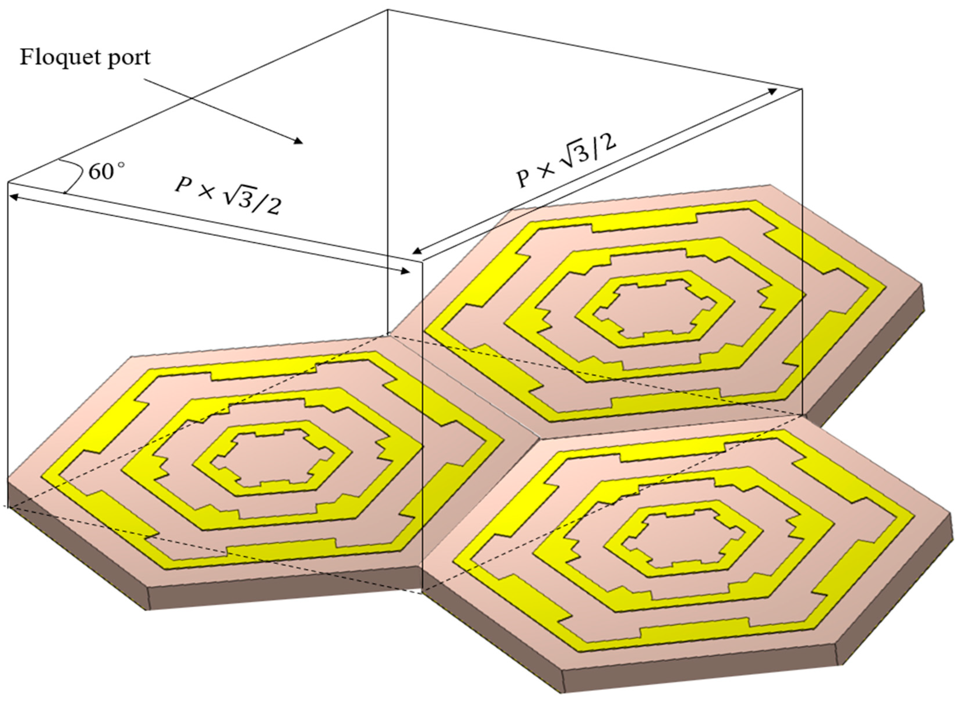
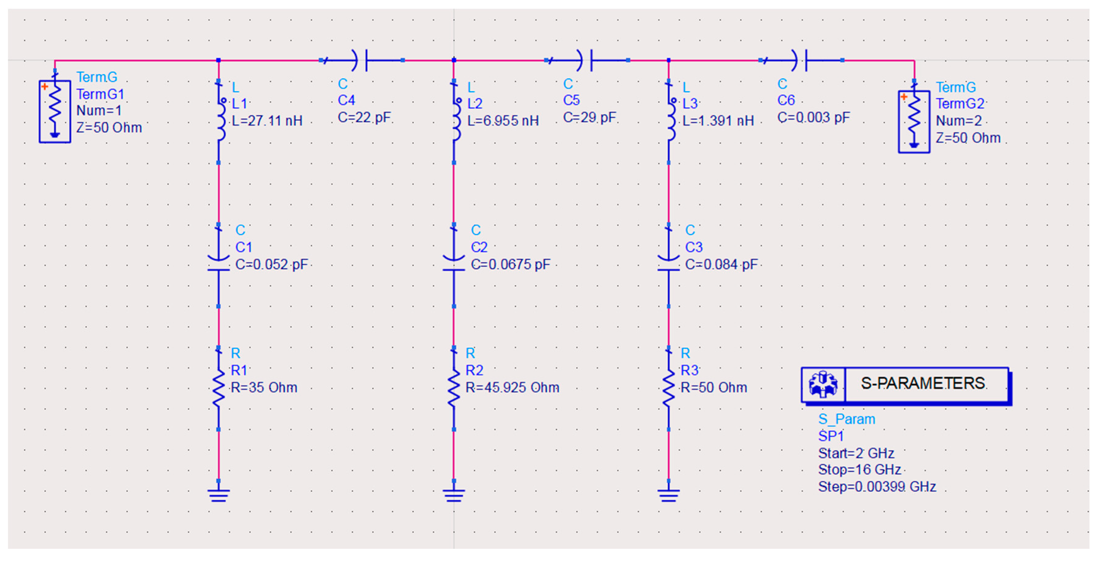
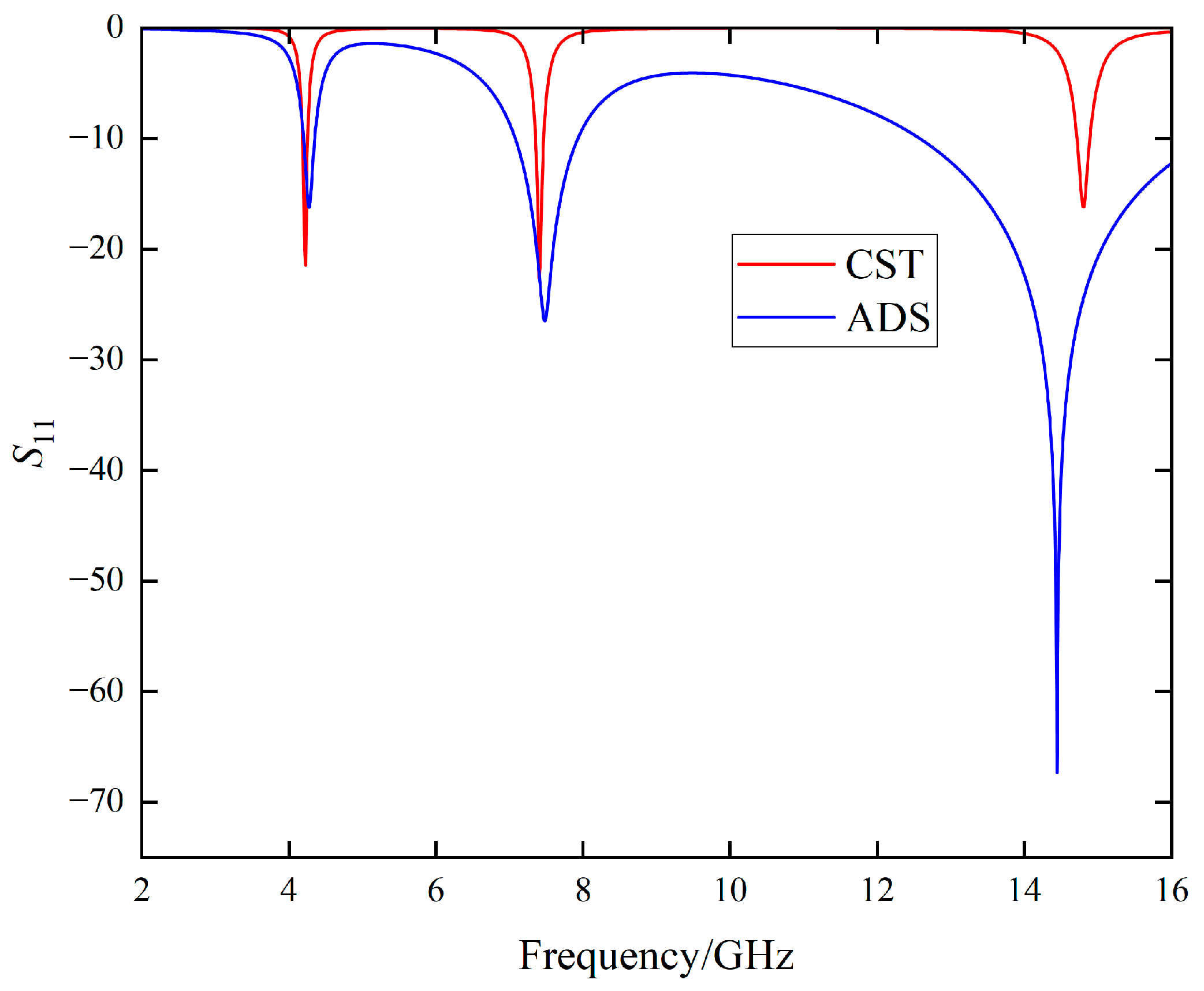
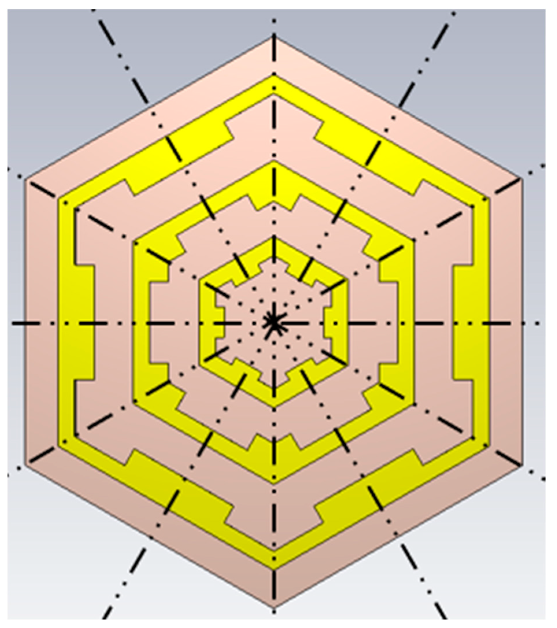
2. Modeling and Theoretical Analysis

The schematic diagram of the structure designed in this paper is shown in Figure 1. Considering the electromagnetic properties and manufacturability, as well as the process of combining different materials, the top and bottom layers are made of copper with a thickness of H1 = 0.035 mm, and the middle dielectric layer is made of FR4 with a thickness of H = 1 mm. The conductivity of copper is 5.8107 S/m, the dielectric constant of FR4 is 4.3, and the loss tangent is 0.025. Different colors are used in Figure 1 to indicate the structural parameters of different layers. Dark blue A, orange B, and blue C correspond to the inner layer, middle layer, and outer layer structure, respectively. The bottom layer is completely covered by copper. The structural parameters after parameter optimization are shown in Table 1. As shown in Figure 2, the overall structure of the MMA is formed by the periodic combination of the unit structure shown in Figure 1. Since the sub-unit adopts a hexagonal shape, the setting of periodic boundary conditions is different from the conventional rectangular boundary condition setting, specifically set to the repetition period in the x direction, which is P × 3 /2; furthermore, the other period direction forms a 60° angle with the x direction, and the repetition period is also P × 3 /2. Strictly speaking, the boundary condition used here is a rectangular periodic boundary condition with an angle, i.e., a parallelogram boundary condition. The hexagonal unit cell extends infinitely in the two-dimensional space through the parallelogram boundary condition, thus forming a honeycomb structure. The schematic diagram of boundary conditions is shown in Figure 3.
The simulation method used is the finite integral method, and the frequency domain solver used is shown in [44,45,46,47,48,49,50,51]. The simulation frequency is set to 2–16 GHz. The incident direction of the plane wave is the negative direction of the Z axis, and the electric field vibration direction is the y direction. These simulation conditions are used as the standard in the following cases, where no explanation is given.
For the structure simulated using the finite integral method [52,53,54,55,56,57,58,59,60], the reflectivity R(ω) and transmittance T(ω) after the incident wave acts on the structure can be calculated by the S parameters, R ω = S 11 2 , T ω = S 21 2 (S11 is the input reflection coefficient, S21 is the transmission coefficient). According to Kirchhoff’s thermal radiation law, the absorption rate can be calculated by the following formula:
A ( ω ) = 1 R ( ω ) T ( ω )
In the designed MMA, the copper covering the bottom layer effectively suppresses the transmission of electromagnetic waves, so the absorption rate can be further simplified to A ω = 1 R ω . The matching of the impedance of the MMA and the vacuum is often considered to be a manifestation of efficient absorption, where the impedance in the vacuum is 377 Ω. This indicates that the electromagnetic energy can enter the structure and be consumed, and there is no reflection or transmission [61,62,63,64,65,66,67,68]. Since the thickness of the MMA (2H + H1 = 1.07 mm) is very small compared to the minimum wavelength (18.75 mm@16 GHz) of the incident wave, based on the equivalent medium theory [69], this MMA can be treated as a homogeneous medium, and its impedance can be described as follows:
Z = μ e f f / ε e f f
where μeff and εeff represent the equivalent permeability and permittivity of MMA, respectively. At the same time, the refractive index and impedance of MMA can be calculated by reflection coefficient S11 and transmission coefficient S21. The formula is as follows:
n = 1 k d cos 1 1 2 S 21 1 S 11 2 + S 21 2 Z = 1 + S 11 2 S 21 2 / 1 S 11 2 S 21 2
where k is the wave vector of the incident wave and d is the total thickness of the MMA, represented as H + 2 × H1(1.07 mm). At the same time, after obtaining the wave impedance and refractive index, the equivalent permittivity and equivalent permeability can be calculated as follows:
ε e f f = n / Z μ eff = n × Z
Generally speaking, when the real part of the impedance is close to 1, the imaginary part is close to 0, and the real and imaginary parts of the equivalent dielectric constant and permeability are close in numerical value, the electromagnetic wave will be perfectly absorbed on the MMA structure.

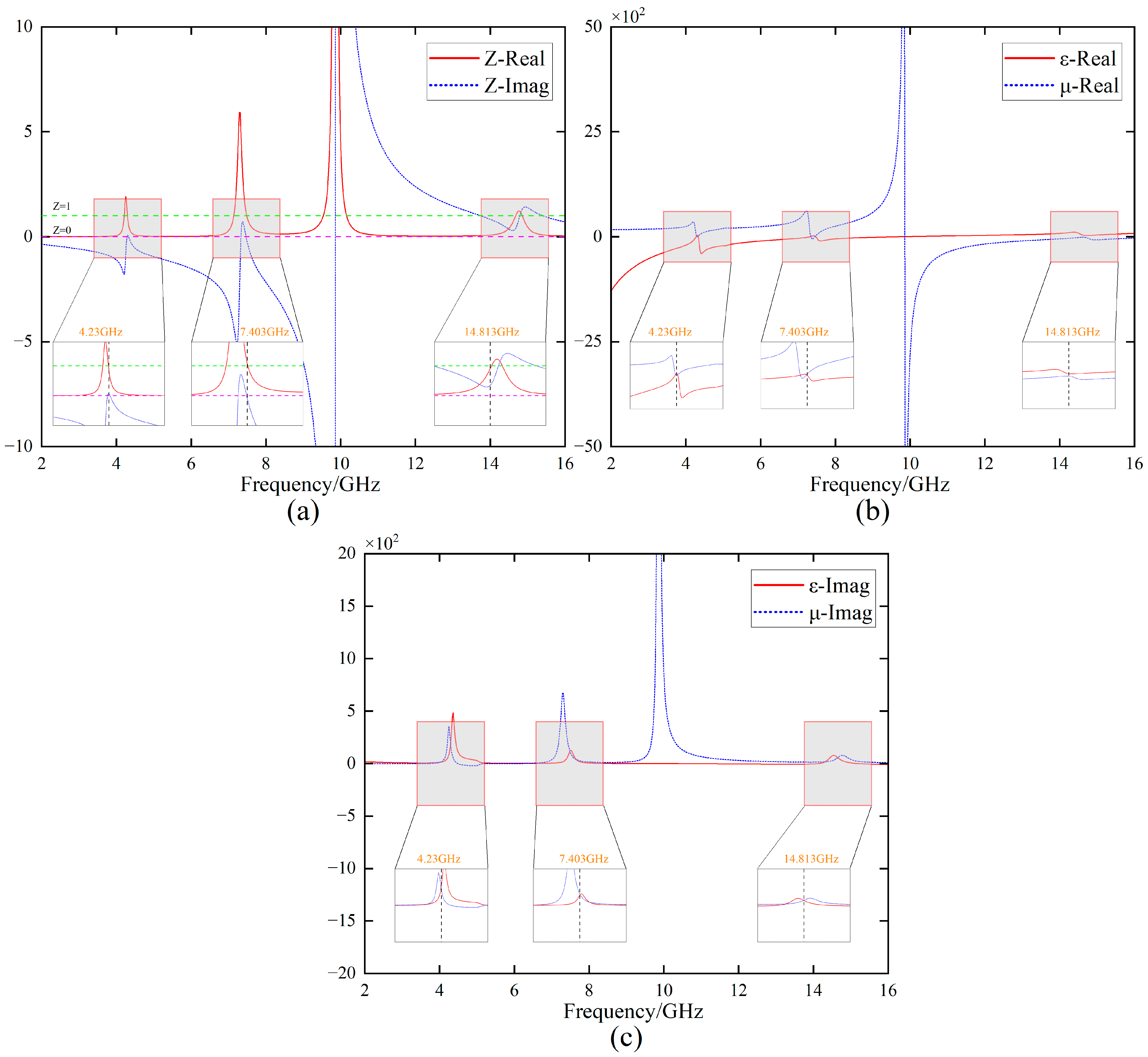
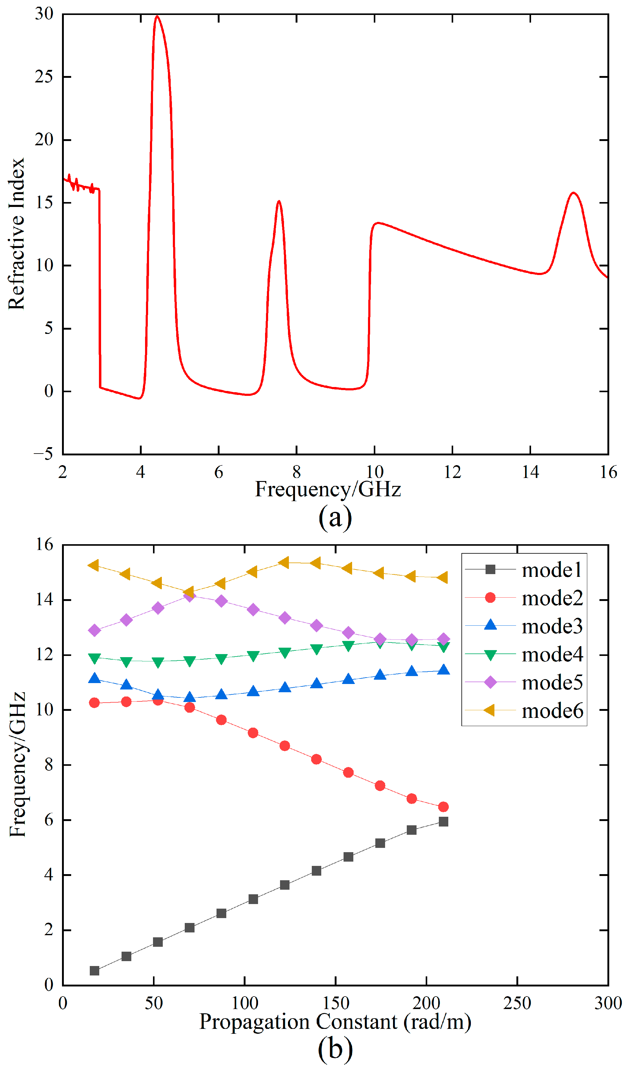
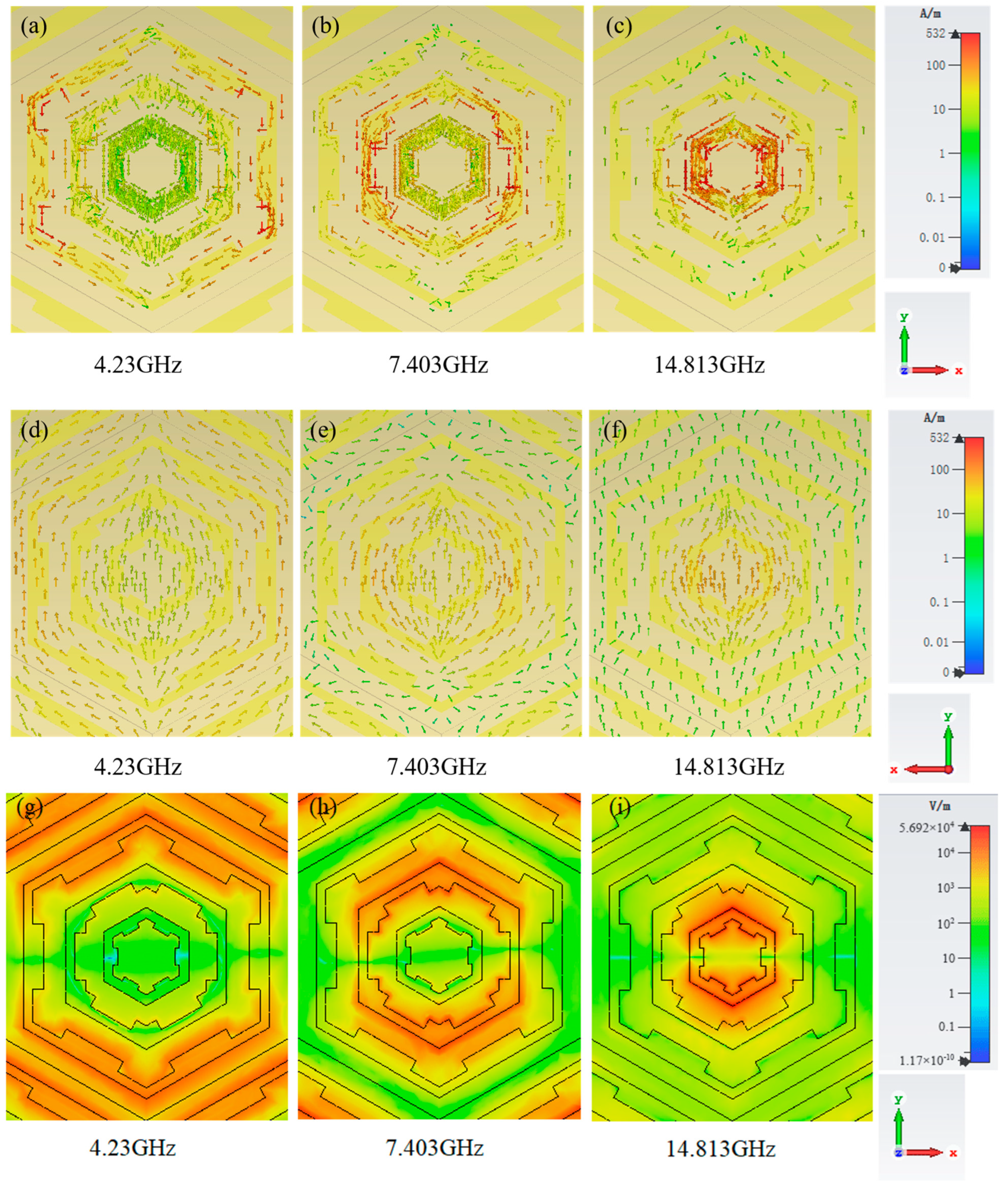
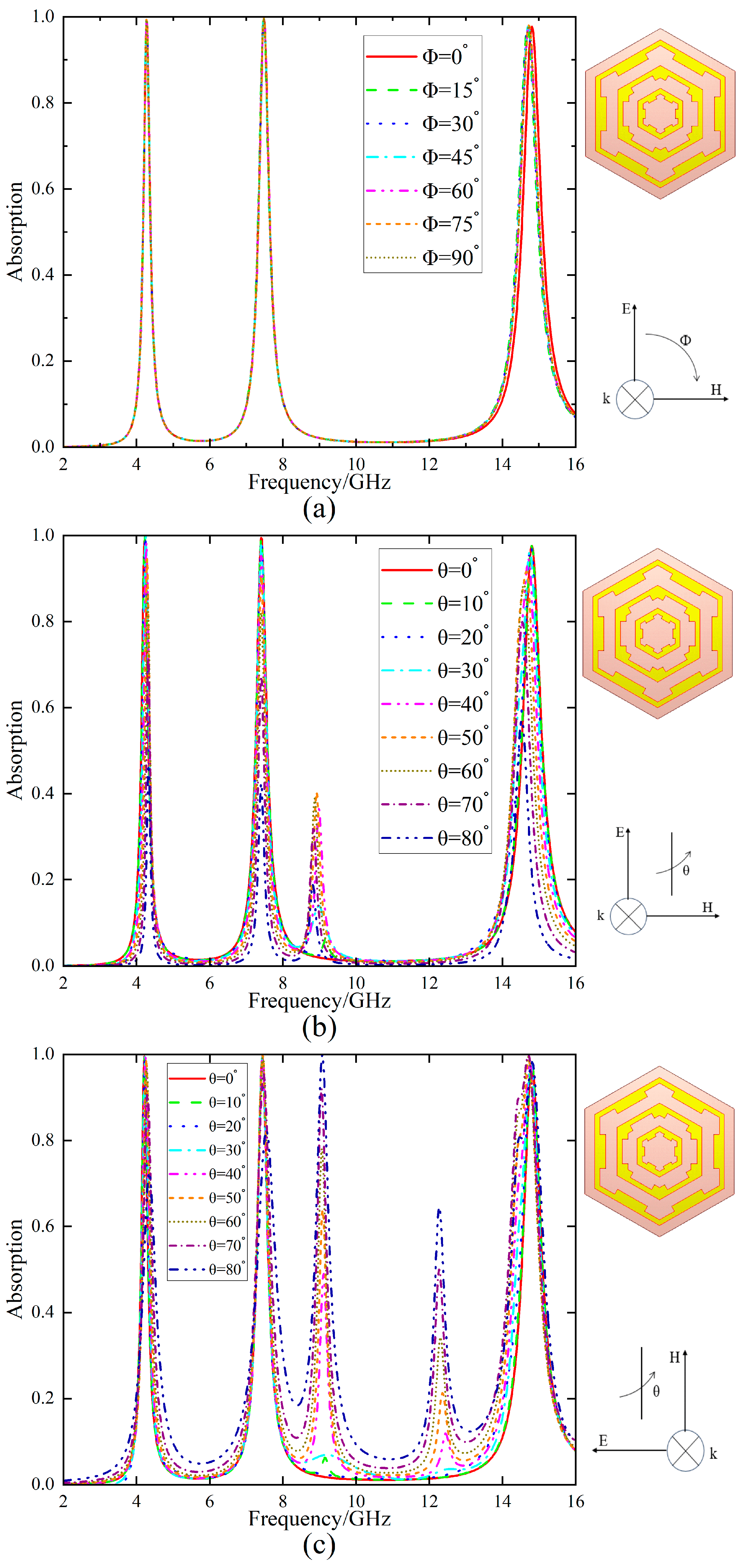
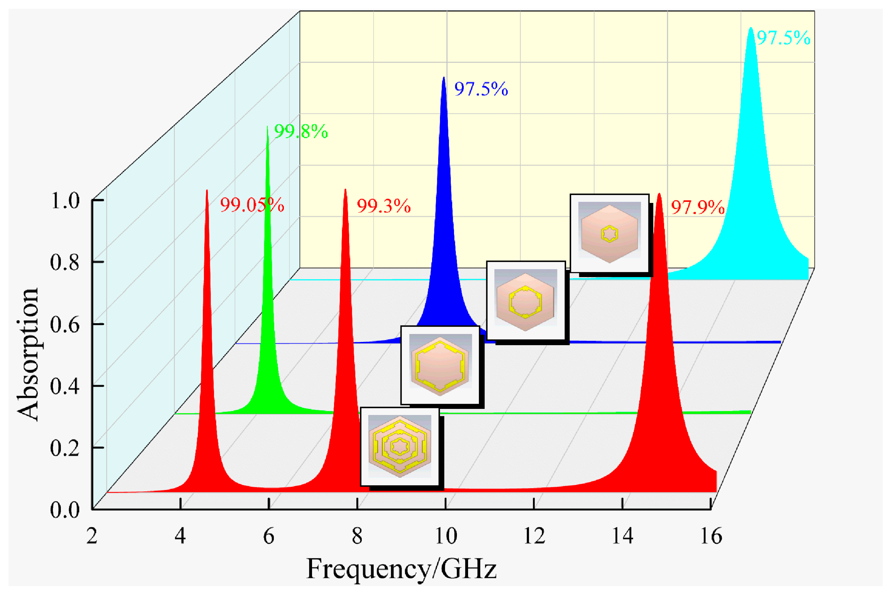
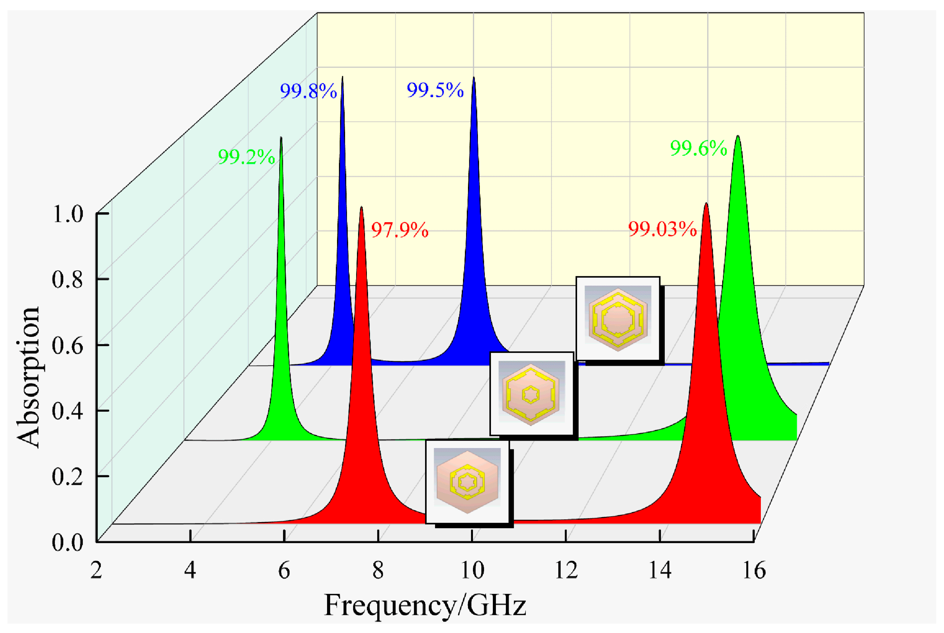
3. Analysis and Discussion

The simulation of MMA using the parameters of Table 1 in the software is shown in Figure 4 for the absorption curve of 2–16 GHz electromagnetic waves. There are three absorption peaks in the figure, located at 4.23 GHz, 7.403 GHz, and 14.813 GHz, respectively, and the corresponding absorption rates reach 99.05%, 99.3%, and 97.9%.
In principle, the refractive index and impedance can be calculated by substituting the S parameters into the above formula, but since S21 appears in the denominator in the inversion formula, S21 is required to be a non-zero value. On the back of the structure, a layer of copper is set to prevent the electromagnetic wave from penetrating, which will make S21 zero, and means that the formula cannot be inverted. After consulting the literature [70], we found that Ye of Zhejiang University mentioned in the article published in PRL that four very small holes can be set on the metal backplane, so that the absorption rate of the structure can be simulated without changing the transmission coefficient S21 to zero. In the simulation process of this article, four round holes with a diameter of 0.02 mm are set on the copper layer under the dielectric layer, so that the subsequent S parameter inversion method can be calculated. The center point of the unit structure is defined as (0, 0), and the coordinate points of the four round holes are (4, 4), (4, −4), (−4, −4), and (−4, 4).
Figure 5a shows the real and imaginary parts of the absorber impedance. It should be noted that the impedance here refers to the impedance relative to vacuum, which is 377 Ω. It can be found that at three absorption frequencies, 4.23 GHz, 7.403 GHz, and 14.813 GHz, the real part of the relative impedance is 1 and the imaginary part is 0. This indicates that near these three frequencies, the absorber achieves impedance matching and fulfills the condition of efficient absorption. Figure 5b and Figure 5c show the comparison of the real and imaginary parts of the equivalent permittivity and equivalent permeability of the absorber, respectively. It can be found that the permittivity and permeability change greatly around 10 GHz. The former changes from a normal negative value to a normal positive value, while the latter changes from a positive value to a negative value. The mutation near 10 GHz will be emphasized in the subsequent analysis of the refractive index and dispersion.
It is worth noting that near 4.23 GHz and 7.403 GHz, the permittivity briefly becomes greater than 0, and the permeability decreases to near 0. Finally, the real and imaginary parts of the permittivity and permeability are consistent near these two frequencies. Consistent with the situation of the first two frequencies, near the third absorption frequency of 14.813 GHz, the permittivity greater than 0 decreases and intersects with the permeability. In addition, near the three absorption frequencies, the real parts of the permittivity and permeability are all negative, which is beneficial for enhancing the absorption performance. The equality of the permittivity and permeability indicates that the electric resonance and magnetic resonance intensities are balanced, which is beneficial for achieving stable electromagnetic resonance and perfect absorption.
As shown in Figure 6a, the refractive index curve shows significant peaks and valleys with increasing frequency, which are associated with the absorption frequencies, respectively. Before 10 GHz, the refractive index changes abruptly at the absorption frequency, and the real part has a higher numerical value, indicating that the first two absorption frequencies correspond to strong local resonance modes. There is no corresponding absorption band near 10 GHz, but the refractive index still changes abruptly, and this change is not accompanied by an obvious decrease, indicating that the absorption mechanism may have changed after 10 GHz. The reason behind this phenomenon can be better understood through Figure 6b. Only modes one and two are distributed below 10 GHz, and the two modes do not overlap, indicating that the first two absorption bands correspond to one mode, respectively, and the absorption mechanisms are similar, both of which are local resonance modes. Between 10 GHz and 16 GHz, the four modes are concentrated in this interval and partially overlap, indicating that the absorption in this interval may rely on multilayer interference or other high-frequency effects.
Next, the surface current and electric field of MMA at the corresponding absorption frequency were simulated to analyze the absorption mechanism. The electric field polarization direction of the plane wave is set to y direction polarization. The corresponding surface current and electric field diagrams at the three frequency points are shown in Figure 7a–i.
First, we will focus on the surface current. As shown in Figure 7a, at 4.23 GHz, the surface current of the upper metal layer is mainly distributed in a ring shape on the outermost structure, while it can be seen in Figure 7d that the current direction of the lower metal layer at 4.23 GHz is opposite to that of the upper metal layer. The currents in the opposite direction on the upper and lower surfaces form a magnetic response. Secondly, we will focus on Figure 7g–i. At 4.23 GHz, the electric field distribution is located in the upper and lower parts of the outermost structure, aligning with the direction of the incident wave’s electric field, which is along the y-axis. The vertical electric field is concentrated within the outermost layer of the structure, indicating that electromagnetic resonance occurs in this layer of the MMA. The electromagnetic field and surface current distributions at 7.403 GHz and 14.813 GHz are very similar to those observed at 4.23 GHz, with these distributions located in the middle and innermost layers, respectively. The electromagnetic resonance generated by the metallic structure on the surface of the MMA, along with the magnetic response formed by the opposing circular currents between the upper and lower metal surfaces, enables efficient absorption of electromagnetic waves at specific frequency points.
The triple-band absorber proposed in this paper can also be analyzed using an equivalent circuit, as shown in Figure 8. From the electric field distribution in Figure 7, it can be observed that, under the influence of the electric field, the electrons in the three-ring structure of the top metasurface undergo directional movement. When excited by electromagnetic waves of different frequencies, each ring can be equivalently modeled as a series connection of an inductor and a capacitor. Additionally, charge accumulation and release occur between adjacent rings within the same subunit, with the equivalent capacitances represented by C4 and C5. The top and bottom metal surfaces are separated by a dielectric, which can be equivalently modeled as capacitance C6. In addition, resistors R1, R2, and R3 are placed in each branch to represent the energy dissipation caused by electromagnetic resonance within the absorber when it is excited by the incident electromagnetic wave. The equivalent circuit was simulated using ADS software, and the two-port S11 results were compared to the full-wave simulation S11 results from CST, as shown in Figure 9. It can be seen that, except for the relatively large deviation at the third absorption peak, the results from both methods show a high level of agreement in the other frequency bands. This fully demonstrates the feasibility of using ADS for equivalent circuit analysis. Furthermore, considering that the equivalent circuit theory of frequency-selective surfaces is essentially an adaptation of antenna theory, the deviation observed at the third absorption peak remains within an acceptable range.
Next, we analyze the polarization sensitivity of the MMA and the impact of different incidence angles on its absorption performance. Figure 10a shows the absorption spectra under a normal incidence of a plane wave as the polarization angle changes. The polarization angle increases from 0 degrees to 90 degrees, with an amplitude of 15 degrees. It can be observed that the MMA’s absorption performance remains almost unchanged for incident waves with different polarizations. This phenomenon occurs because the designed MMA has a high degree of geometric symmetry, as shown in Figure 11. This high symmetry ensures that the energy loss caused by electromagnetic resonance and the magnetic response within the MMA remains consistent for incident waves with varying polarizations, indicating that the MMA is polarization-insensitive [71].
Figure 10b and Figure 10c show the absorption spectra for TE and TM incident waves at different incidence angles, respectively. For TM waves, the incident wave retains all magnetic field components. As the incidence angle increases from 0° to 80° in 10° increments, all three absorption peaks remain clearly visible. As shown in Figure 10c and Table 2, when the incidence angle increases from 0° to 70°, the absorption efficiency of the three peaks remains above 90%, maintaining a high level. Only when the incidence angle reaches 80° does the absorption efficiency at around 4.3 GHz and 7.5 GHz drop to 72.6% and 82.2%, respectively, while the absorption efficiency at 14.8 GHz remains largely unchanged, staying above 97%. On the other hand, as the incidence angle exceeds 30°, two new absorption peaks emerge between the second and third absorption peaks. The absorption efficiency of these new peaks increases with the incidence angle, reaching over 90% and 60% when the angle reaches 80°. The appearance of these new peaks can be attributed to additional electromagnetic resonances occurring at other frequencies between the electromagnetic wave and the fixed MMA structure under oblique incidence, resulting in secondary absorption peaks.
For TE waves, as shown in Figure 10b and Table 3, the situation is similar to that of TM waves. The difference is that when the incident angle of TM waves reaches 80°, the absorption efficiency of the first two absorption peaks drops to below 90%, while when the incident angle of TE waves changes to 60°, the absorption efficiency of the three absorption peaks has greatly attenuated, dropping to below 90%. When the incident angle increases to 80°, the absorption efficiency of the three absorption peaks is further reduced to 46.7%, 72.4%, and 57.1%. Compared to the TM wave, the absorption efficiency of the first and third absorption peaks decreased by more than 50%. The reason for this phenomenon may be that the electromagnetic field vector directions of TM waves and TE waves are perpendicular, and the structures of MMA in the X and Y directions are different. The MMA arranged in a honeycomb shape is compactly arranged in the X direction. In the case of oblique incidence, the electromagnetic response generated by adjacent units will not be greatly affected, while the spacing between adjacent MMA units in the Y direction is larger (nearly 10 mm). Under normal incidence, such an arrangement will not have a significant impact on the absorption efficiency, while under oblique incidence, MMA will not be able to generate a stable electromagnetic response at the original absorption frequency due to its relatively sparse arrangement, thus exhibiting significantly deteriorated absorption characteristics.
The metallic structure on the top surface consists of the following three parts: inner, middle, and outer sections; specifically, there are three concentric hexagonal rings with different details and sizes. To analyze the impact of these individual structures on absorption performance, the simulation results of each separate section are compared to those of the complete structure. The corresponding absorption curves and schematic diagrams of these structures are shown in Figure 12.
As shown in Figure 12, the three structures from the outside to the inside correspond to the three absorption peaks, from low-frequency to high-frequency, respectively, which indicates that the large-sized structure corresponds to the lower frequency absorption frequency point. It can be seen that the absorption near 4 GHz and 14 GHz does not differ significantly before and after separation, while the absorption efficiency at 7.479 GHz, in the middle, drops from 99.3% to 97.5% after separation. This indicates that the absorption efficiency of a single absorption peak does not depend solely on the corresponding structure, and the absorption performance of the middle ring also depends on the coupling between adjacent structures.
In addition, the absorption performance of the double-ring structure was compared, as shown in Figure 13. There are three combination modes of the double-ring structure, namely, inner-middle, inner-outer, and middle-outer. The inner-middle ring achieves absorption efficiency of 97.9% and 99.03% at 7.384 GHz and 14.813 GHz, respectively; the inner-outer ring has an absorption efficiency of 99.2% at 4.211 GHz and 99.6% GHz at 14.642 GHz; and the middle-outer ring has two absorption frequencies of 4.268 GHz and 7.441 GHz, and the corresponding absorption efficiencies are 99.8% and 99.5%. It can be found that with the change in the combination mode, the absorption frequency and absorption efficiency do not change significantly, which indicates that the coupling between the inner, middle, and outer rings does not weaken the absorption performance.
Table 4 compares the proposed triple-band metasurface absorber with the published research results in related fields in recent years. It can be found that the proposed structure is the only absorber that works in the C-band and Ku-band, and the absorption efficiency in the C-band exceeds 99%. In addition, the thickness of the absorber is only 1.07 mm, which is 0.0154 times the wavelength corresponding to the minimum absorption frequency, and it has entered the sub-wavelength range. Other meta-unit cells all adopt square units, while this paper adopts a honeycomb regular hexagon sub-structure. Compared to the square structure, the regular hexagon structure has a higher close-packing degree, and more absorbing units can be placed on the unit area. The proposed triple-band metasurface absorber has polarization-insensitive characteristics. For obliquely incident TE and TM waves, the absorption efficiency can be maintained above 90% when the incident angle is less than 50 degrees and 70 degrees, respectively. The authors believe that the proposed metasurface absorber can be applied in the fields of television, broadcasting, and satellite communication.

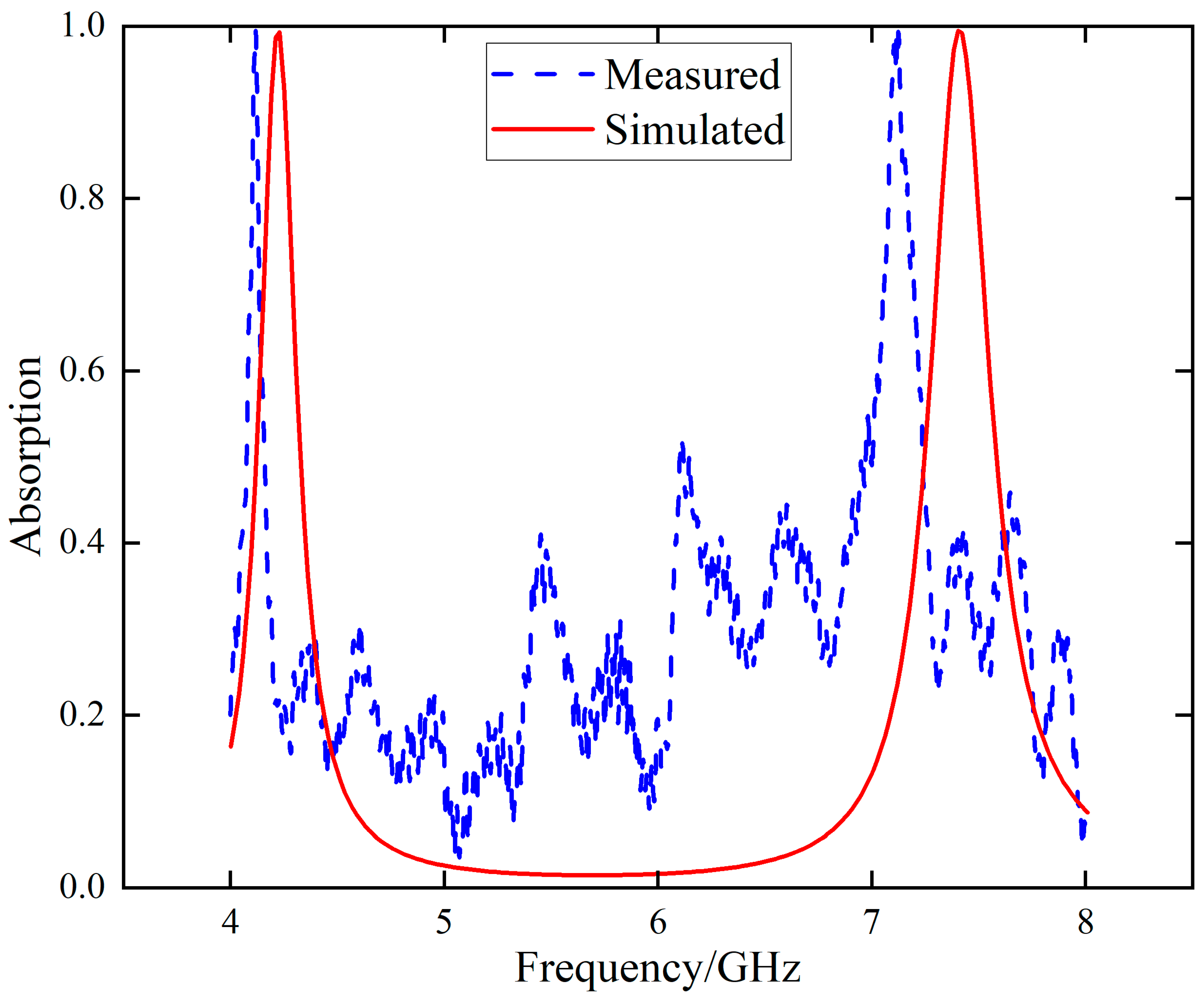
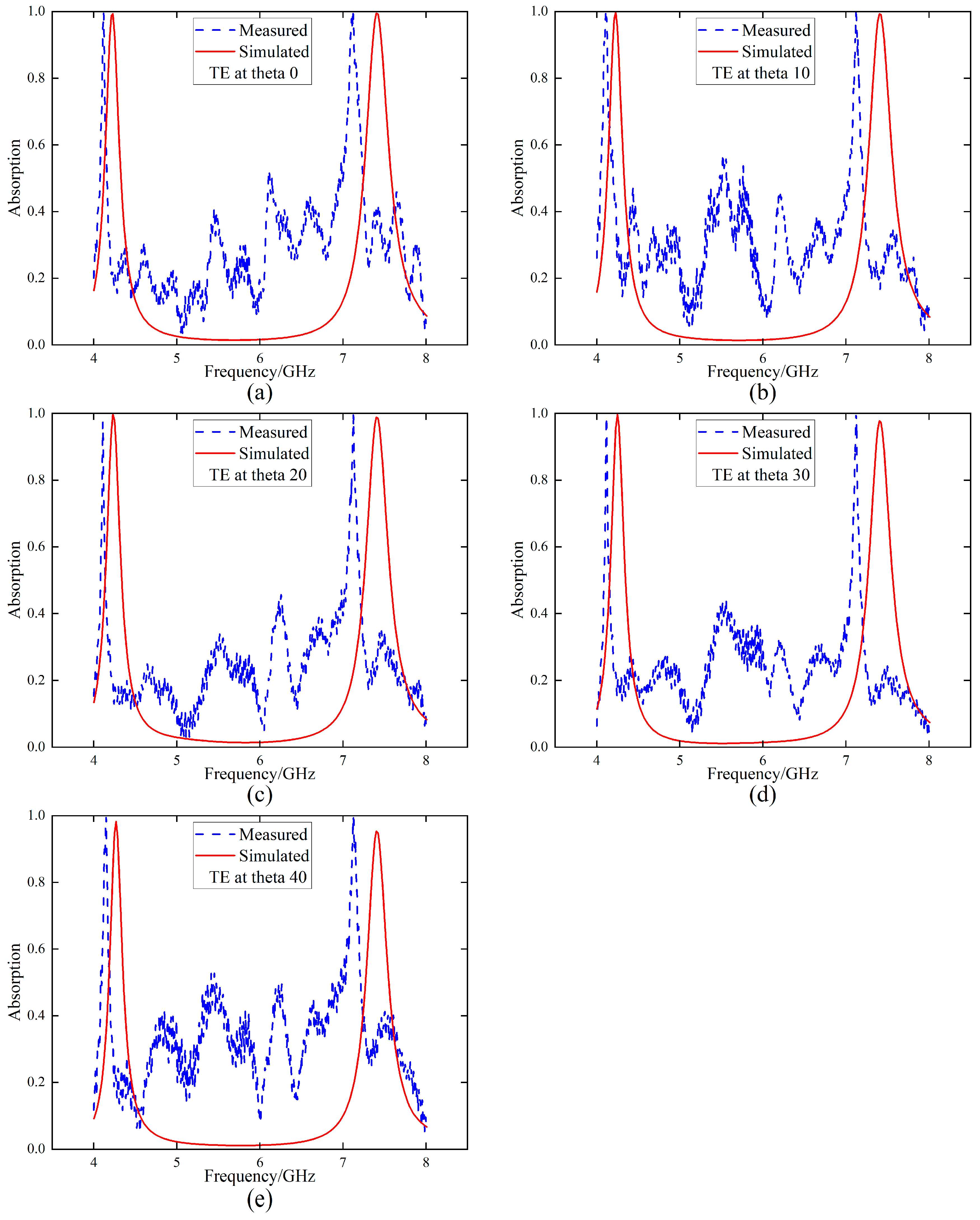
4. Experiment and Verification

The sample fabricated by the PCB printing process is shown in Figure 14a, and the experimental facilities and environment are shown in Figure 14b [79,80,81,82,83,84,85,86]. The absorption performance of the sample is tested using the free space method, with the schematic diagram depicted in Figure 14c. The output port and input port of the vector network analyzer (VNA) are connected to the transmitting antenna and receiving antenna, respectively. In this experiment, the distance between the metasurface and the horn antenna was set to 35 cm. The electromagnetic wave emitted by the transmitting antenna is reflected and absorbed on the surface of the sample. The reflected energy is collected by the receiving antenna and input into the VNA to obtain the reflection coefficient S11 curve. Since a layer of copper is laid on the back of the sample, the electromagnetic wave will not pass through the sample; therefore, the reflection coefficient can be used to evaluate the absorption performance [87,88,89,90]. By normalizing the reflection coefficient, the absorption rate can be obtained.
Firstly, the measured and simulated absorption diagram of MMA under normal incidence is shown in Figure 15. Due to the limitations of the experimental conditions, the transmitting horn can only emit electromagnetic waves of 4–8 GHz, so only the first two absorption peaks can be tested. From the absorption diagram, it is evident that the fabricated MMA achieved absorption efficiencies of 99.5% at 4.12 GHz and 99.4% at 7.123 GHz, with deviations of 0.11 GHz and 0.28 GHz, respectively. Considering the errors caused by the manufacturing process and experimental conditions, this degree of absorption frequency shift is acceptable.
Then, the TE wave oblique incidence experiment was carried out, and the incident angle was changed from 0° to 40°, with a step length of 10°. The corresponding absorption diagram is shown in Figure 16. The absorption frequency charts obtained from the simulation and experiment are shown in Table 5. As can be seen, with the increase in the incident angle, the absorption frequencies obtained from the simulation remain at 4.23 GHz and 7.403 GHz, while the absorption frequencies from the experiment shift from 4.12 GHz and 7.123 GHz to 4.149 GHz and 7.126 GHz, respectively. As shown in Table 5, there is always a deviation of approximately 0.1 GHz and 0.2 GHz between the simulated and tested absorption frequencies, which may be caused by process errors and experimental conditions. It should be noted that the test results indicate that with the increase in the incident angle, the two absorption frequencies do not shift by more than 0.3 GHz, suggesting that the absorption characteristics of this MMA do not degrade significantly with changes in the incident angle.

5. Conclusions

This paper proposes a triple-band metamaterial absorber based on metal–dielectric–metal. The simulation results show that the structure achieves 97% absorption efficiency at 4.23 GHz, 7.403 GHz, and 14.813 GHz. By changing the polarization angle and incident angle of the incident plane wave, the MMA exhibits polarization-insensitive and wide-angle absorption characteristics. The absorption mechanism is explained by the equivalent medium theory, impedance matching, and the equivalent circuit. At the absorption frequency, the structure satisfies impedance matching and electromagnetic parameter matching. The analysis of the electromagnetic field and surface current distribution shows that the absorption process of MMA is mainly completed by the magnetic response formed by the reverse current between the upper and lower surfaces and the electromagnetic resonance on the upper metal surface. Then, the influence of different parts of the structure on the absorption performance is analyzed, and the three independent parts on the upper surface of the structure correspond to three different absorption peaks. Finally, the MMA’s performance is validated through experiments, and the experimental results align closely with the simulation outcomes. The MMA proposed in this paper can be applied in the inter-satellite communications, achieving functions such as electromagnetic shielding and stealth.

Author Contributions

Conceptualization, S.Z. and X.J.; methodology, T.Z.; software, S.Z.; validation, S.Z., M.G. and G.F.; formal analysis, S.Z.; investigation, S.Z.; data curation, S.Z.; writing—original draft preparation, S.Z.; writing—review and editing, X.J.; visualization, M.Z.; supervision, X.J. All authors have read and agreed to the published version of the manuscript.

Funding

This work was supported in part by the Science and Technology Innovation Leading Talent Project of Special Support plan for high-level talents in Zhejiang Province (2021R52032); in part by the Natural Science Foundation of Zhejiang Province under grant No. ZCLZ25F0502; and in part by the Zhejiang University Students Science and Technology Innovation Activity Plan-New Talent Plan (2024R409C054).

Institutional Review Board Statement

Not applicable.

Informed Consent Statement

Not applicable.

Data Availability Statement

The data that support the findings of this study are available from the corresponding author upon reasonable request.

Conflicts of Interest

The authors declare no conflict of interest.

References

  1. Wang, Y.; Liu, Z.; Zhou, F.; Yi, Z.; Wang, J. Perfect absorption properties of a near-infrared super-surface perfect absorber based on a multilayer subwavelength array structure. Phys. Lett. A 2025, 540, 130395. [Google Scholar] [CrossRef]
  2. Sun, Z.; Zhao, J.; Zhou, Z.; Gao, Q. L1 model-driven recursive multi-scale denoising network for image super-resolution. Knowl. Based Syst. 2021, 225, 107115. [Google Scholar] [CrossRef]
  3. Zhao, J.; Chen, C.; Zhou, Z.; Cao, F. Single image super-resolution based on adaptive convolutional sparse coding and convolutional neural networks. J. Vis. Commun. Image Represent. 2019, 58, 651–661. [Google Scholar] [CrossRef]
  4. Zhao, J.; Chen, N.; Zhou, Z. A temporal sparse collaborative appearance model for visual tracking. Multimed. Tools Appl. 2020, 79, 14103–14125. [Google Scholar] [CrossRef]
  5. Zhao, J.; Huang, T.; Zhou, Z.; Cao, F. A Compact Recursive Dense Convolutional Network for image classification. Neurocomputing 2020, 372, 8–16. [Google Scholar] [CrossRef]
  6. Zhao, J.; Lu, Y.; Zhou, Z. Correlation filters based on temporal regularization and background awareness. Comput. Electr. Eng. 2020, 86, 106757. [Google Scholar] [CrossRef]
  7. Zhao, J.; Lv, Y.; Zhou, Z.; Cao, F. A novel deep learning algorithm for incomplete face recognition: Low-rank-recovery network. Neural Netw. 2017, 94, 115–124. [Google Scholar] [CrossRef] [PubMed]
  8. Zhao, J.; Sun, T.; Cao, F. Image super-resolution via adaptive sparse representation and self-learning. IET Comput. Vis. 2018, 12, 753–761. [Google Scholar] [CrossRef]
  9. Zhao, J.; Zhang, W.; Cao, F. Robust object tracking using a sparse coadjutant observation model. Multimed. Tools Appl. 2018, 77, 30969–30991. [Google Scholar] [CrossRef]
  10. Zhou, Z.; Xue, B.; Wang, H.; Zhao, J. Bidirectional Multi-scale Deformable Attention for Video Super-Resolution. Multimed. Tools Appl. 2024, 83, 27809–27830. [Google Scholar] [CrossRef]
  11. Zhou, Z.; Zhang, W.; Zhao, J. Robust visual tracking using discriminative sparse collaborative map. Int. J. Mach. Learn. Cybern. 2019, 10, 3201–3212. [Google Scholar] [CrossRef]
  12. Tao, H.; Landy, N.I.; Bingham, C.M.; Zhang, X.; Averitt, R.D.; Padilla, W.J. A metamaterial absorber for the terahertz regime: Design, fabrication and characterization. Opt. Express 2008, 16, 7181–7188. [Google Scholar] [CrossRef] [PubMed]
  13. Taya, S.A. Dispersion properties of lossy, dispersive, and anisotropic left-handed material slab waveguide. Optik 2015, 126, 1319–1323. [Google Scholar] [CrossRef]
  14. Taya, S.A.; Colak, I.; Suthar, B.; Ramahi, O.M. Cancer cell detector based on a slab waveguide of anisotropic, lossy, and dispersive left-handed material. Appl. Opt. 2021, 60, 8360–8367. [Google Scholar] [CrossRef]
  15. Chen, Z.; Cheng, S.; Zhang, H.; Yi, Z.; Tang, B.; Chen, J.; Zhang, J.; Tang, C. Ultra wideband absorption absorber based on Dirac semimetallic and graphene metamaterials. Phys. Lett. A 2024, 517, 129675. [Google Scholar] [CrossRef]
  16. Cheng, S.; Li, W.; Zhang, H.; Akhtar, M.N.; Yi, Z.; Zeng, Q.; Ma, C.; Sun, T.; Wu, P.; Ahmad, S. High sensitivity five band tunable metamaterial absorption device based on block like Dirac semimetals. Opt. Commun. 2024, 569, 130816. [Google Scholar] [CrossRef]
  17. Li, W.; Cheng, S.; Yi, Z.; Zhang, H.; Song, Q.; Hao, Z.; Sun, T.; Wu, P.; Zeng, Q.; Raza, R. Advanced optical reinforcement materials based on three-dimensional four-way weaving structure and metasurface technology. Appl. Phys. Lett. 2025, 126, 033503. [Google Scholar] [CrossRef]
  18. Li, W.; Cheng, S.; Zhang, H.; Yi, Z.; Tang, B.; Ma, C.; Wu, P.; Zeng, Q.; Raza, R. Multi-functional metasurface: Ultra-wideband/multi-band absorption switching by adjusting guided-mode resonance and local surface plasmon resonance effects. Commun. Theor. Phys. 2024, 76, 065701. [Google Scholar] [CrossRef]
  19. Li, W.; Yi, Y.; Yang, H.; Cheng, S.; Yang, W.; Zhang, H.; Yi, Z.; Yi, Y.; Li, H. Active tunable terahertz bandwidth absorber based on single layer graphene. Commun. Theor. Phys. 2023, 75, 045503. [Google Scholar] [CrossRef]
  20. Li, Z.; Cheng, S.; Zhang, H.; Yang, W.; Yi, Z.; Yi, Y.; Wang, J.; Ahmad, S.; Raza, R. Ultrathin broadband terahertz metamaterial based on single-layer nested patterned graphene. Phys. Lett. A 2025, 534, 130262. [Google Scholar] [CrossRef]
  21. Zeng, Z.; Liu, H.; Zhang, H.; Cheng, S.; Yi, Y.; Yi, Z.; Wang, J.; Zhang, J. Tunable ultra-sensitive four-band terahertz sensors based on Dirac semimetals. Photonics Nanostruct.-Fundam. Appl. 2025, 63, 101347. [Google Scholar] [CrossRef]
  22. Cheng, Y.; Cao, W.; He, X. Hybrid Plasmonic Waveguides with Tunable ENZ Phenomenon Supported by 3D Dirac Semimetals. Laser Photonics Rev. 2024, 18, 2400167. [Google Scholar] [CrossRef]
  23. Liu, S.; Cao, W.; Jiang, S.; He, L.; Lin, F.; He, X. 3D Dirac Semimetal Supported Tunable Multi-Frequency Terahertz Metamaterial Absorbers. Adv. Quantum Technol. 2024, 7, 2300386. [Google Scholar] [CrossRef]
  24. Wang, G.; Cao, W.; He, X. 3D Dirac Semimetal Elliptical Fiber Supported THz Tunable Hybrid Plasmonic Waveguides. IEEE J. Sel. Top. Quantum Electron. 2023, 29, 3284231. [Google Scholar] [CrossRef]
  25. Corbitt, S.J.; Francoeur, M.; Raeymaekers, B. Implementation of optical dielectric metamaterials: A review. J. Quant. Spectrosc. Radiat. Transf. 2015, 158, 3–16. [Google Scholar] [CrossRef]
  26. Dewangan, L.; Patinavalasa, M.S.; Acharjee, J.; Solunke, Y.; Ghosh, S.; Mishra, N.K. Broadband metamaterial absorber for stealth applications at K-band. AEU-Int. J. Electron. Commun. 2023, 170, 154828. [Google Scholar] [CrossRef]
  27. Saadeldin, A.S.; Sayed, A.M.; Amr, A.M.; Sayed, M.O.; Hameed, M.F.O.; Obayya, S.S.A. Broadband polarization insensitive metamaterial absorber. Opt. Quantum Electron. 2023, 55, 652. [Google Scholar] [CrossRef]
  28. Sharma, A.; Singh, H.; Gupta, A. Design and development of high-performance metamaterial absorber for moisture-sensing application. Appl. Phys. A 2023, 129, 377. [Google Scholar] [CrossRef]
  29. Yoon, Y.; Lim, D.; Tentzeris, M.M.; Lim, S. Low-cost metamaterial absorber using three-dimensional circular truncated cone. Microw. Opt. Technol. Lett. 2018, 60, 1622–1630. [Google Scholar] [CrossRef]
  30. Kumar, R.; Singh, B.K.; Pandey, P.C. Cone-shaped resonator-based highly efficient broadband metamaterial absorber. Opt. Quantum Electron. 2023, 55, 579. [Google Scholar] [CrossRef]
  31. Armghan, A.; Aliqab, K.; Alsharari, M. Polarization and wide-angle incidence MXene-based metamaterial absorber for visible and infrared wavelengths. Opt. Quantum Electron. 2024, 56, 1265. [Google Scholar] [CrossRef]
  32. Huang, X.; Chen, Y.; Chen, S.; Yang, K.; Liang, J.; Zhou, Z.; Dai, W. Ultrasensitive and tunable multi-narrowband metamaterial absorber. Results Phys. 2023, 47, 106364. [Google Scholar] [CrossRef]
  33. Abdalla, M.A.; Choudhary, D.K.; Chaudhary, R.K. A compact reconfigurable bandpass/lowpass filter with independent transmission zeros based on generalized NRI metamaterial. Int. J. RF Microw. Comput. Aided Eng. 2020, 30, e22074. [Google Scholar] [CrossRef]
  34. Kukreja, J.; Choudhary, D.K.; Chaudhary, R.K. A Metamaterial Inspired ZOR Antenna Using IDC and Spiral Inductor with Partial Ground Plane for WLAN Application. Wirel. Pers. Commun. 2019, 107, 137–147. [Google Scholar] [CrossRef]
  35. Garg, P.; Jain, P. Novel ultrathin penta-band metamaterial absorber. AEU-Int. J. Electron. Commun. 2020, 116, 153063. [Google Scholar] [CrossRef]
  36. Hannan, S.; Islam, M.T.; Faruque, M.R.I.; Rmili, H. Polarization-independent perfect metamaterial absorber for C, X and, Ku band applications. J. Mater. Res. Technol. 2021, 15, 3722–3732. [Google Scholar] [CrossRef]
  37. Al-Khafaji, R.M.; AbdulAmeer, S.A.; Husain, A.; Al Mashhadani, Z.I.; Ali, B.M.; Abdulkadhim, A.H.; Albahash, Z.F. On mechanical behavior and optimization of elliptical-rectangular absorbers made by ABS and PLA in both experimental and numerical methods. J. Braz. Soc. Mech. Sci. Eng. 2023, 45, 383. [Google Scholar] [CrossRef]
  38. Narkis, M.; Shach-Caplan, M.; Haba, Y.; Silverstein, M.S. PVC modification through polymerization of a monomer absorbed in porous suspension-type PVC particles. J. Vinyl Addit. Technol. 2004, 10, 109–120. [Google Scholar] [CrossRef]
  39. Kim, J.H.; Lee, S.-G.; Kim, T.-T.; Ha, T.; Lee, S.H.; Kim, J.-H.; Lee, Y.H. High-temperature differences in plasmonic broadband absorber on PET and Si substrates. Sci. Rep. 2020, 10, 13279. [Google Scholar] [CrossRef]
  40. Han, W.; Park, Q.H. Broadband absorber with dispersive metamaterials. Nanophotonics 2023, 12, 2443–2449. [Google Scholar] [CrossRef]
  41. Laur, V.; Maalouf, A.; Chevalier, A.; Comblet, F. Three-Dimensional Printing of Honeycomb Microwave Absorbers: Feasibility and Innovative Multiscale Topologies. IEEE Trans. Electromagn. Compat. 2021, 63, 390–397. [Google Scholar] [CrossRef]
  42. Kshirsagar, D.E.; Dubey, H.; Puri, V.; Sharon, M.; Sharon, M. X-band absorber carbon microbeads. Mater. Lett. 2021, 299, 130054. [Google Scholar] [CrossRef]
  43. Yang, H.; Zhang, J.; Shen, Z. Water-based metamaterial absorber for temperature modulation. Phys. Scr. 2024, 99, 105563. [Google Scholar] [CrossRef]
  44. AbdelAll, N.; Almokhtar, M.; Khouqeer, G.; Abood, I.; El Soliman, S. Rainbow Trapping with Engineered Topological Corner States and Cavities in Photonic Crystals. Adv. Quantum Technol. 2024, 7, 2400050. [Google Scholar] [CrossRef]
  45. Istokskaia, V.; Lefebvre, B.; Versaci, R.; Dreghici, D.B.; Doria, D.; Grepl, F.; Olšovcová, V.; Schillaci, F.; Stanček, S.; Tryus, M.; et al. Real-time bremsstrahlung detector as a monitoring tool for laser–plasma proton acceleration. High Power Laser Sci. Eng. 2024, 12, e57. [Google Scholar] [CrossRef]
  46. Li, S.; Fang, Y.; Wang, J. Control of light–matter interactions in two-dimensional materials with nanoparticle-on-mirror structures. Opto-Electron. Sci. 2024, 3, 240011. [Google Scholar] [CrossRef]
  47. Liang, M.; Lu, D.; Ma, Y. Vectorial optical fields manipulation via metasurfaces. Opto-Electron. Eng. 2024, 51, 240068. [Google Scholar] [CrossRef]
  48. Luo, Z.; Ding, Y.; Peng, F.; Wei, G.; Wang, Y.; Wu, S.-T. Ultracompact and high-efficiency liquid-crystal-on-silicon light engines for augmented reality glasses. Opto-Electron. Adv. 2024, 7, 240039. [Google Scholar] [CrossRef]
  49. Peters, C.; Forbes, A. Controlling the hidden parity in vectorial light with metasurfaces. Adv. Photonics 2024, 6, 040501. [Google Scholar] [CrossRef]
  50. Rane, S.; Prabhu, S.; Chowdhury, D.R. Physics and applications of terahertz metagratings. Opto-Electron. Sci. 2024, 3, 230049. [Google Scholar] [CrossRef]
  51. Zhang, S.; Li, H.; Fan, C.; Zeng, Z.; Xiong, C.; Wu, J.; Yan, Z.; Liu, D.; Sun, Q. Adaptive decentralized AI scheme for signal recognition of distributed sensor systems. Opto-Electron. Adv. 2024, 7, 240119. [Google Scholar] [CrossRef]
  52. Md Sadman Sakib, R.; Aydogan, O. Physics and artificial intelligence: Illuminating the future of optics and photonics. Adv. Photonics 2024, 6, 050500. [Google Scholar] [CrossRef]
  53. Seo, J.; Jo, J.; Kim, J.; Kang, J.; Kang, C.; Moon, S.-W.; Lee, E.; Hong, J.; Rho, J.; Chung, H. Deep-learning-driven end-to-end metalens imaging. Adv. Photonics 2024, 6, 066002. [Google Scholar] [CrossRef]
  54. Shi, J.; Yang, C.; Chen, Y.; Wang, T.; Yu, H.; Cao, J.; Geng, Z.; Wang, Z.; Wen, H.; Tan, H.; et al. Precise mode control of mid-infrared high-power laser diodes using on-chip advanced sawtooth waveguide designs. High Power Laser Sci. Eng. 2024, 12, e42. [Google Scholar] [CrossRef]
  55. Taha, B.A.; Addie, A.J.; Haider, A.J.; Chaudhary, V.; Apsari, R.; Kaushik, A.; Arsad, N. Exploring Trends and Opportunities in Quantum-Enhanced Advanced Photonic Illumination Technologies. Adv. Quantum Technol. 2024, 7, 2300414. [Google Scholar] [CrossRef]
  56. Wang, H.; He, Y.; Zhu, H.; Dong, H.; Wang, S. Research progress and prospects of metasurface polarization devices. Opto-Electron. Eng. 2024, 51, 240095. [Google Scholar] [CrossRef]
  57. Wu, Y.; Yang, Q.; Shen, B.; Tao, Y.; Zhang, X.; Tao, Z.; Xing, L.; Ge, Z.; Li, T.; Bai, B.; et al. Multifunctional mixed analog/digital signal processor based on integrated photonics. Opto-Electron. Sci. 2024, 3, 240012. [Google Scholar] [CrossRef]
  58. Yang, H.; He, H.; Hu, Y.; Duan, H. Metasurface-empowered vector light field regulation, detection and application. Opto-Electron. Eng. 2024, 51, 240168. [Google Scholar] [CrossRef]
  59. Yu, Z.; Li, M.; Xing, Z.; Gao, H.; Liu, Z.; Pu, S.; Mao, H.; Cai, H.; Ma, Q.; Ren, W.; et al. Genetic algorithm assisted meta-atom design for high-performance metasurface optics. Opto-Electron. Sci. 2024, 3, 240016. [Google Scholar] [CrossRef]
  60. Zhou, L.; Lou, H.; Deng, Z.; Qin, X.; Pan, J.; Di, Y.; Gu, C.; Luo, D.; Li, W. Compact mid-infrared dual-comb spectrometer over 3–4 μm via intra-pulse difference frequency generation in LiNbO3 waveguides. High Power Laser Sci. Eng. 2024, 12, e23. [Google Scholar] [CrossRef]
  61. Berhe, A.M.; As’ham, K.; Al-Ani, I.; Hattori, H.T.; Miroshnichenko, A.E. Strong coupling and catenary field enhancement in the hybrid plasmonic metamaterial cavity and TMDC monolayers. Opto-Electron. Adv. 2024, 7, 230181. [Google Scholar] [CrossRef]
  62. Nan, T.; Zhao, H.; Guo, J.; Wang, X.; Tian, H.; Zhang, Y. Generation of structured light beams with polarization variation along arbitrary spatial trajectories using tri-layer metasurfaces. Opto-Electron. Sci. 2024, 3, 230052. [Google Scholar] [CrossRef]
  63. Refaeli, Z.; Marcus, G.; Shamir, Y. A simple method for pulse contrast enhancement via self-focusing. High Power Laser Sci. Eng. 2024, 12, e18. [Google Scholar] [CrossRef]
  64. Shen, C.-Y.; Li, J.; Li, Y.; Gan, T.; Bai, L.; Jarrahi, M.; Ozcan, A. Multiplane quantitative phase imaging using a wavelength-multiplexed diffractive optical processor. Adv. Photonics 2024, 6, 056003. [Google Scholar] [CrossRef]
  65. Ullah, M.; Mikki, S. Optical Nonreciprocity in a Multimode Cavity Optomechanical System Controlled by Dynamic Casimir Force. Adv. Quantum Technol. 2024, 7, 2400007. [Google Scholar] [CrossRef]
  66. Zhang, C.-L.; Hu, K.-X.; Zhang, J.; Cao, J.; Zhang, S.; Wang, H.-F. Topological Phase Transition and Edge States with Tunable Localization in the Cyclic Four-Mode Optical System. Adv. Quantum Technol. 2024, 7, 2400165. [Google Scholar] [CrossRef]
  67. Zhang, J.C.; Chen, M.K.; Fan, Y.; Chen, Q.; Chen, S.; Yao, J.; Liu, X.; Xiao, S.; Tsai, D.P. Miniature tunable Airy beam optical meta-device. Opto-Electron. Adv. 2024, 7, 230171. [Google Scholar] [CrossRef]
  68. Zhang, Y.; Chen, Y.; Wang, T.; Zhu, Q.; Gu, M. Ultrahigh performance passive radiative cooling by hybrid polar dielectric metasurface thermal emitters. Opto-Electron. Adv. 2024, 7, 230194. [Google Scholar] [CrossRef]
  69. Smith, D.R.; Vier, D.C.; Koschny, T.; Soukoulis, C.M. Electromagnetic parameter retrieval from inhomogeneous metamaterials. Phys. Rev. E 2005, 71, 036617. [Google Scholar] [CrossRef]
  70. Ye, D.; Wang, Z.; Xu, K.; Li, H.; Huangfu, J.; Wang, Z.; Ran, L. Ultrawideband Dispersion Control of a Metamaterial Surface for Perfectly-Matched-Layer-Like Absorption. Phys. Rev. Lett. 2013, 111, 187402. [Google Scholar] [CrossRef]
  71. Zhou, F.; Ji, C.; Liu, Z.; Jiang, N. Polarization-desensitization dynamically adjustable quintuple plasmon-induced transparency multi-frequency modulator based on graphene metamaterial. J. Appl. Phys. 2024, 136, 143107. [Google Scholar] [CrossRef]
  72. Jorwal, S.; Dubey, A.; Gupta, R.; Agarwal, S. Triple-Band Ultrathin Minkowski Fractal-Inspired Polarization-Insensitive Microwave Absorber for Stealth Application. J. Electron. Mater. 2024, 53, 8171–8179. [Google Scholar] [CrossRef]
  73. Shukoor, M.A.; Kumar, V.; Dey, S. Compact polarisation insensitive wide angular stable triple band absorber for RF energy harvesting, RCS reduction, and sensor applications. Int. J. RF Microw. Comput. Aided Eng. 2021, 31, e22763. [Google Scholar] [CrossRef]
  74. Genikala, S.; Ghosh, A.; Roy, B. Triple band single layer microwave absorber based on closed loop resonator structures with high stability under oblique incidence. AEU-Int. J. Electron. Commun. 2023, 164, 154629. [Google Scholar] [CrossRef]
  75. Amugothu, R.; Damera, V. Wide incidence angle triple-band metamaterial EM wave absorber at X and Ku frequency band applications. J. Electromagn. Waves Appl. 2023, 37, 1208–1220. [Google Scholar] [CrossRef]
  76. Berka, M.; Fellah, B.; Islam, T.; Bendaoudi, A.; Das, S.; Mahdjoub, Z.; Tarricone, L. A triple band square-interlinked-rhombus shaped metamaterial absorber for microwave C and X-band utilizations. Opt. Quantum Electron. 2023, 55, 1223. [Google Scholar] [CrossRef]
  77. Mishra, N.; Choudhary, D.K.; Chowdhury, R.; Kumari, K.; Chaudhary, R.K. An Investigation on Compact Ultra-Thin Triple Band Polarization Independent Metamaterial Absorber for Microwave Frequency Applications. IEEE Access 2017, 5, 4370–4376. [Google Scholar] [CrossRef]
  78. Hossain, M.B.; Faruque, M.R.I.; Islam, M.T.; Singh, M.; Jusoh, M. Triple band microwave metamaterial absorber based on double E-shaped symmetric split ring resonators for EMI shielding and stealth applications. J. Mater. Res. Technol. 2022, 18, 1653–1668. [Google Scholar] [CrossRef]
  79. Cheng, H.; Fang, B.; Huang, W.; Li, R.; Shen, C.; Ke, L.; Jing, X.; Li, C.; Hong, Z. Far-field steering of beams based on dynamic encoding metasurface. Opt. Laser Technol. 2022, 156, 108520. [Google Scholar] [CrossRef]
  80. Jing, X.; Gui, X.; Zhou, P.; Hong, Z. Physical Explanation of Fabry–Pérot Cavity for Broadband Bilayer Metamaterials Polarization Converter. J. Light. Technol. 2018, 36, 2322–2327. [Google Scholar] [CrossRef]
  81. Jing, X.; Tang, X.; Tian, Y.; Kong, Z.; Li, C.; Shen, C.; Hong, Z. Enhancement of Diffraction Efficiency Based on the Addition Principle of Coded Digital Gratings. J. Light. Technol. 2022, 40, 136–142. [Google Scholar] [CrossRef]
  82. Qin, G.; Dong, Y.; Zhang, P.; Liu, J.; Li, C.; Huang, W.; Hong, Z.; Shen, C.; Jing, X. Broadband absorber coupled with anti-reflection inverted pyramid type all-dielectric microstructure. Opt. Lasers Eng. 2023, 160, 107288. [Google Scholar] [CrossRef]
  83. Wang, Q.; Li, C.; Fang, B.; Ke, L.; Lu, J.; Ma, X.; Hong, Z.; Jing, X. Flexible and Independent Control of Asymmetric Vortex Beams Based on Spin Multiplexing all Dielectric Metasurface. J. Light. Technol. 2023, 41, 7098–7104. [Google Scholar] [CrossRef]
  84. Xia, R.; Jing, X.; Gui, X.; Tian, Y.; Hong, Z. Broadband terahertz half-wave plate based on anisotropic polarization conversion metamaterials. Opt. Mater. Express 2017, 7, 977–988. [Google Scholar] [CrossRef]
  85. Zeng, B.; Li, C.; Cheng, H.; Fang, B.; Lu, J.; Ma, X.; Wang, L.; Hong, Z.; Jing, X. Anisotropic programmable metasurface beam splitter based on diode real-time control. Opt. Lasers Eng. 2023, 169, 107723. [Google Scholar] [CrossRef]
  86. Zhao, J.; Jing, X.; Wang, W.; Tian, Y.; Zhu, D.; Shi, G. Steady method to retrieve effective electromagnetic parameters of bianisotropic metamaterials at one incident direction in the terahertz region. Opt. Laser Technol. 2017, 95, 56–62. [Google Scholar] [CrossRef]
  87. Jiang, L.; Fang, B.; Yan, Z.; Fan, J.; Qi, C.; Liu, J.; He, Y.; Li, C.; Jing, X.; Gan, H.; et al. Terahertz high and near-zero refractive index metamaterials by double layer metal ring microstructure. Opt. Laser Technol. 2020, 123, 105949. [Google Scholar] [CrossRef]
  88. Jiang, L.; Fang, B.; Yan, Z.; Li, C.; Fu, J.; Gan, H.; Hong, Z.; Jing, X. Improvement of unidirectional scattering characteristics based on multiple nanospheres array. Microw. Opt. Technol. Lett. 2020, 62, 2405–2414. [Google Scholar] [CrossRef]
  89. Jing, X.; Xu, Y.; Gan, H.; He, Y.; Hong, Z. High Refractive Index Metamaterials by Using Higher Order Modes Resonances of Hollow Cylindrical Nanostructure in Visible Region. IEEE Access 2019, 7, 144945–144956. [Google Scholar] [CrossRef]
  90. Wang, W.; Jing, X.; Zhao, J.; Li, Y.; Tian, Y. Improvement of accuracy of simple methods for design and analysis of a blazed phase grating microstructure. Opt. Appl. 2017, 47, 183–198. [Google Scholar] [CrossRef]
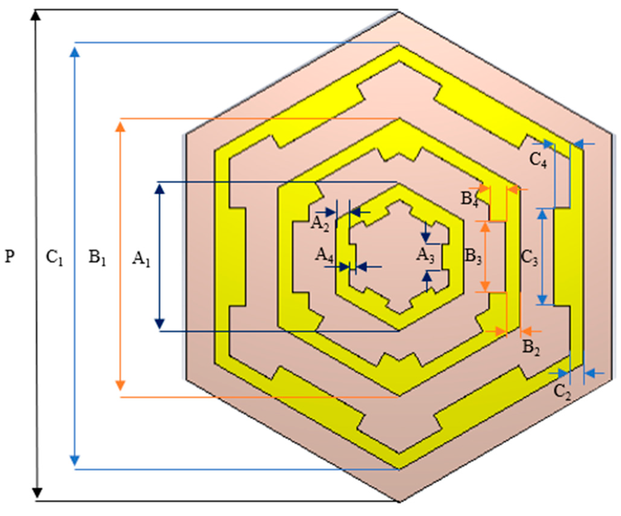
Figure 1. Top view of the MMA.
Photonics 12 00386 g001
Figure 2. Schematic diagram of periodic MMA.
Photonics 12 00386 g002
Figure 3. Schematic diagram of boundary conditions.
Photonics 12 00386 g003
Figure 4. Absorption spectrum diagram of the MMA.
Photonics 12 00386 g004
Figure 5. Wave impedance and equivalent parameters diagram: (a) comparison of the real and imaginary parts of impedance; (b) comparison of the real parts of the equivalent permittivity and permeability; (c) comparison of the imaginary parts of the equivalent permittivity and permeability.
Photonics 12 00386 g005
Figure 6. Refractive index and dispersion diagram: (a) refractive index diagram; (b) dispersion diagram.
Photonics 12 00386 g006
Figure 7. Distribution diagrams of electric fields and surface currents: (a) surface current of the upper layer at 4.23 GHz; (b) surface current of the upper metal layer at 7.403 GHz; (c) surface current of the upper metal layer at 14.813 GHz; (d) surface current of the lower metal layer at 4.23 GHz; (e) surface current of the lower metal layer at 7.403 GHz; (f) surface current of the lower metal layer at 14.813 GHz; (g) electric field distribution at 4.23 GHz; (h) electric field distribution at 7.403 GHz; (i) electric field distribution at 14.813 GHz.
Photonics 12 00386 g007
Figure 8. The equivalent circuit of the proposed absorber. Here, C1 = 0.052 pF, C2 = 0.0675 pF, C3 = 0.084 pF, C4 = 22 pF, C5 = 29 pF, C6 = 0.003 pF, L1 = 27.11 nH, L2 = 6.955 nH, L3 = 1.391 nH, R1 = 35 Ω, R2 = 45.925 Ω, R3 = 50 Ω.
Photonics 12 00386 g008
Figure 9. Comparison of S11 curves from CST and ADS.
Photonics 12 00386 g009
Figure 10. Absorption efficiency diagrams at different polarization angles and incidence angles: (a) absorption efficiency at different polarization angles; (b) absorption efficiency of TE waves at different incidence angles; (c) absorption efficiency of TM waves at different incidence angles.
Photonics 12 00386 g010
Figure 11. Schematic diagram of MMA symmetry.
Photonics 12 00386 g011
Figure 12. Absorption efficiency diagram for single component of MMA.
Photonics 12 00386 g012
Figure 13. Absorption efficiency diagram for double-ring structure.
Photonics 12 00386 g013
Figure 14. Photograph of the MMA, experimental environment, and schematic diagram of the test principle: (a) photograph; (b) experimental environment; (c) schematic diagram of the test principle.
Photonics 12 00386 g014
Figure 15. Absorption comparison of the simulated and measured response under normal incidence.
Photonics 12 00386 g015
Figure 16. Absorption comparison of the simulated and measured response under oblique incidence: (a) theta = 0, (b) theta = 10, (c) theta = 20, (d) theta = 30, and (e) theta = 40.
Photonics 12 00386 g016
Table 1. Diagram of structural parameters.
ParameterSize/mmParameterSize/mmParameterSize/mmParameterSize/mm
A14.5B18.5C113P15
A20.433B20.433C20.433H1
A30.8B32.15C33H10.035
A40.22B40.5C40.5
Table 2. Absorption peak frequencies and absorption rates at different incidence angles for TM wave oblique incidence.
Degree/°First Absorption PeakSecond Absorption PeakThird Absorption Peak
Frequency/GHzAbsorption/%Frequency/GHzAbsorption/%Frequency/GHzAbsorption/%
04.2199.67.4499.614.8197.6
104.2199.37.4499.614.8097.7
204.2399.77.4499.714.8098.3
304.2399.47.4499.814.7898.0
404.2599.77.4499.914.7498.2
504.2399.07.4499.914.7298.7
604.2996.87.4699.214.7099.4
704.3190.87.4695.414.7299.9
804.3472.67.5482.214.8198.2
Table 3. Absorption peak frequencies and absorption rates at different incidence angles for TE wave oblique incidence.
Degree/°First Absorption PeakSecond Absorption PeakThird Absorption Peak
Frequency/GHzAbsorption/%Frequency/GHzAbsorption/%Frequency/GHzAbsorption/%
04.2399.37.4099.514.8197.6
104.2399.77.4099.314.8097.6
204.2399.77.4098.914.7897.6
304.2599.77.4097.714.7696.3
404.2798.27.4095.314.7294.4
504.2994.67.4090.614.6791.6
604.3186.87.4082.014.5688.6
704.3371.57.4067.314.5579.9
804.3346.77.4072.414.5357.1
Table 4. Comparison of the proposed work and the other literature works.
RefAbsorption Frequency (GHz)Frequency BandAbsorptivityUnit Cell Thickness
(mm)
Unit Cell Size (mm)Polarization InsensitivityAngular Stability
[72]2.5, 5.2, 9.8, and 11.0S, C, and X90%, 91%, 97%, and 94%1.6
(0.013λ0)
19 × 19
(0.18λ0 × 0.18λ0)
60°60° for TE and TM
[73]4.9, 10, and 14.05C, X, and Ku99.53%, 99.76%, and 98.71%0.8
(0.013λ0)
10 × 10
(0.163λ0 × 0.163λ0)
Yes45° for TE and 75 for TM
[74]2.4, 5.5, and 7.5S and C99.53%, 99.33%, and 99.90%1.6
(0.0128λ0)
15.1 × 15.1
(0.12λ0 × 0.12λ0)
Yes52° for TE and TM
[75]11.6, 14.04, and 16.56X and Ku99.88%, 99.72%, and 96.41%1.6
(0.0618λ0)
13 × 13
(0.425λ0 × 0.425λ0)
Yes60° for TE and TM
[76]5.86, 6.57, and 8.94C and X86.23%, 92.92%, and 82.07%1.52
(0.029λ0)
10 × 10
(0.19λ0 × 0.19λ0)
Yes90° for TE and TM
[77]4.19, 9.34, and 11.48C and X99.67%, 99.48%, and 99.42%0.8
(0.011λ0)
8 × 8
(0.11λ0 × 0.11λ0)
Yes60° for TE and TM
[78]5.376, 10.72, and 12.25C, X, and Ku99.9%, 99.9%, and 99.7%1.6
(0.028λ0)
10 × 10
(0.179λ0 × 0.179λ0)
No30° for TE and TM
This work4.306, 7.479, and 14.661C and Ku99.05%, 99.3%, and 97.9%1.07
(0.0154λ0)
6 × 7.5 × 7.5 × 3 2   ×   1 2   =
146 mm2
(6 × 0.108λ0 × 0.108λ0 ×   3 2   × 1 2 )
Yes50° for TE and 70° for TM
Table 5. Comparison table of the first two absorption frequencies of simulation and experiment.
SimulationExperiment
Theta = 0Theta = 0Theta = 0Theta = 0Theta = 0
First Absorption peak/GHz4.2304.1204.1094.1094.1164.149
Second Absorption peak/GHz7.4037.1237.1217.1247.1217.126
Disclaimer/Publisher’s Note: The statements, opinions and data contained in all publications are solely those of the individual author(s) and contributor(s) and not of MDPI and/or the editor(s). MDPI and/or the editor(s) disclaim responsibility for any injury to people or property resulting from any ideas, methods, instructions or products referred to in the content.

