Article

Characterization and Degradation of Perovskite Mini-Modules

1
Center for Energy, AIT Austrian Institute of Technology, 1210 Vienna, Austria
2
FOSS Research Centre for Sustainable Energy, University of Cyprus, 1678 Nicosia, Cyprus
3
Department of Physics, College of Science, Kuwait University, Sabah Al Salem University City Campus, Farwaniya 85700, Kuwait
4
Thin Film PV Technology–Partner in Solliance, IMO-IMOMEC, IMEC, 3600 Genk, Belgium
5
EnergyVille, IMO-IMOMEC, 3600 Genk, Belgium
6
IMO-IMOMEC, Hasselt University, 3500 Hasselt, Belgium
*
Author to whom correspondence should be addressed.
Inorganics 2024, 12(8), 219; https://doi.org/10.3390/inorganics12080219
Submission received: 4 July 2024 / Revised: 2 August 2024 / Accepted: 8 August 2024 / Published: 15 August 2024
(This article belongs to the Special Issue The State of the Art of Research on Perovskites Materials)

Abstract

:
Organic–inorganic hybrid metal halide perovskites are poised to revolutionize the next generation of photovoltaics with their exceptional optoelectronic properties and compatibility with low-cost and large-scale fabrication methods. Since perovskite tends to degrade over short time intervals due to various parameters (oxygen, humidity, light, and temperature), advanced characterization methods are needed to understand their degradation mechanisms. In this context, investigation of the electrical and optoelectronic properties of several perovskite mini-modules was performed by means of photo- and electroluminescence imaging as well as Dark Lock-In Thermography methods. Current–voltage curves at periodic time intervals and External Quantum Efficiency measurements were implemented alongside other measurements to reveal correlations between the electrical and radiative properties of the solar cells. The different imaging techniques used in this study reveal the changes in radiative emission processes and how those are correlated with performance. Alongside the indoor optoelectronic characterization of perovskite reference samples, the outdoor monitoring of two perovskite modules of the same structure for 23 weeks is reported. Significant performance degradation is presented outdoors from the first week of testing for both samples under test. The evolution of the major electrical characteristics of the mini-modules and the diurnal changes were studied in detail. Finally, dark storage recovery studies after outdoor exposure were implemented to investigate changes in the major electrical parameters.

1. Introduction

The leap forward in power conversion efficiency (PCE) enabled by lead halide perovskites is unprecedented, with PCEs starting from 3.8% in its first study to a current certified value of 25.5% in single-junction and 33.7% in perovskite–silicon tandem devices [1]. The main challenge for the successful commercialization of perovskite solar cells is to achieve high stability at the module level [2,3]. The commercially available solar modules undergo a series of characterization procedures that analyze their properties and ensure their quality [4]. However, these procedures and protocols cannot unambiguously be applied to perovskite solar modules (PSMs), due to their unpredictable degradation mechanisms.
Optical techniques such as electroluminescence (EL), photoluminescence (PL), and transient absorption spectroscopy [5] are valuable and non-destructive measurement techniques for the investigation of local radiative/non-radiative charge recombination processes, thus allowing the investigation of cracks, defects, shunts, and stacking faults in cells and modules. Larger-scale defects and shunts comprise variations of series resistances, stoichiometry variations, and differences in interface recombination properties [6,7,8,9].
So far, only a limited number of studies have been conducted on outdoor performance monitoring of perovskite-based devices [10,11,12,13,14,15]. Outdoor stability testing has been reported for different types of perovskite devices, including single-junction cells [16,17], modules [12,18], and tandem cells [19,20]. A systematic investigation of perovskite performance and measurements under real outdoor conditions and related with indoor characterization studies is still needed to reach commercialization.
In the presented work, we employed both indoor optoelectronic characterization methods and investigation of stability outdoors to understand the degradation of perovskite mini-modules. Understanding the radiative properties as well as the evolution of electrical characteristics of perovskite outdoors is required for improving knowledge of these devices and maximizing the cell’s efficiency.

2. Materials and Methods

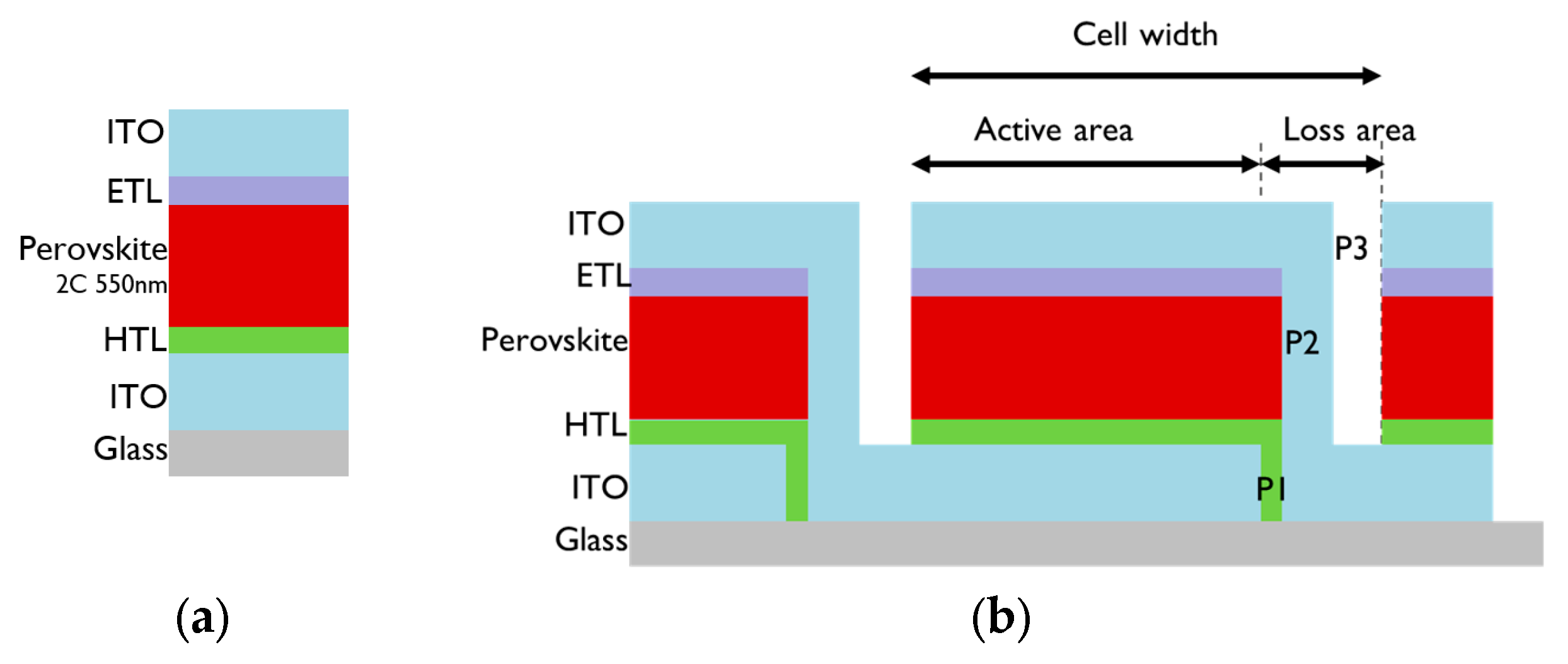
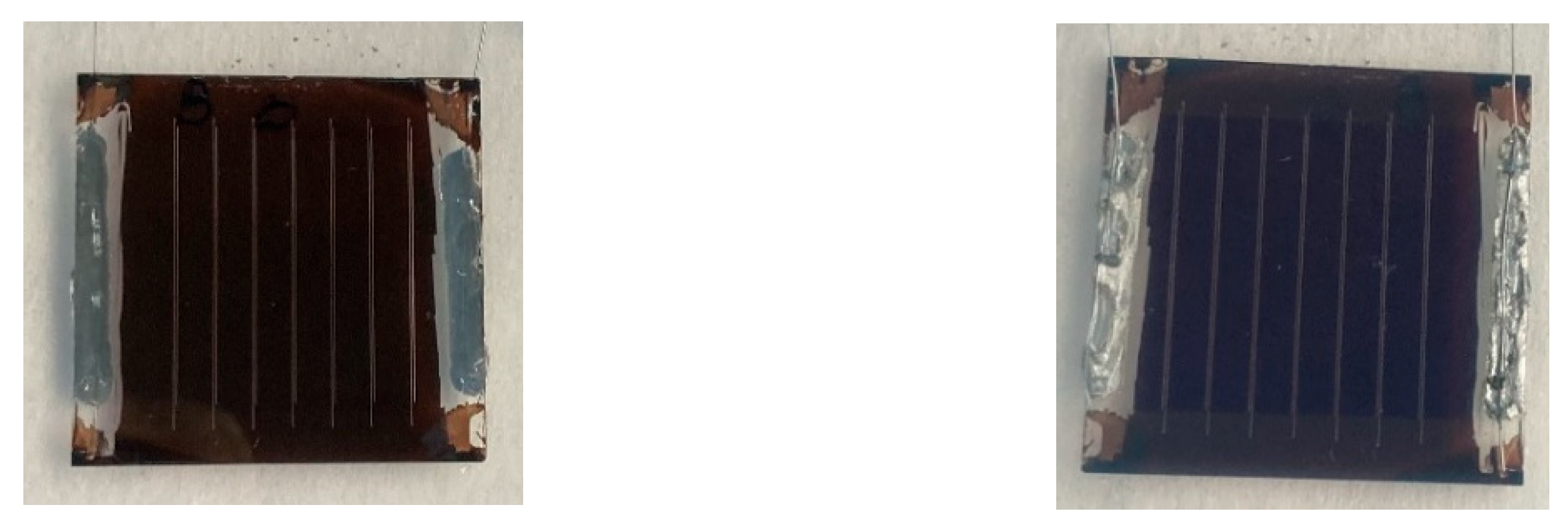
2.1. Perovskite Mini-Modules

The perovskite mini-modules studied presented a double-cation/double-halide perovskite active layer with the composition Cs0.18FA0.82PbI2.82Br0.18. To make large-area devices, the mini-modules were produced by laser scribing, to generate 7 sub-cells connected in series. To prevent penetration of metallic particles of the top electrode into the soft perovskite layer, ITO (indium–tin–oxide) was used. ITO was also selected as a top electrode to obtain semi-transparent modules. The module stack was as follows: glass/ITO/hole transport layer (HTL)/560 nm 2C perovskite with a bandgap of 1.6 eV/electron transport layer (ETL)/ITO/glass. The hole transport layer (HTL) and perovskite layer were processed from the solution by spin coating. PTAA (poly(triaryl amine)) was employed as the HTL. A combination of LiF/C60/BCP was chosen as the ETL. Fullerene (C60) is well known as an ETL, while the LiF improved the perovskite/C60 interface and BCP improved the energy level alignment between C60 and the metal electrode.
Figure 1 depicts the structure of the perovskite sub-cell and the cross-section of the mini-module. Figure 2 shows the front and back sides of one perovskite mini-module (substrate size: 10 cm × 10 cm and active area size: 2 cm × 2 cm). Four perovskite mini-modules (labeled as S9, S10, S11, and S12) were utilized as reference samples and kept indoors (in the dark) under ambient conditions for frequent characterization using DLIT, EL, and PL methods alongside IV measurements. Two identical samples to those used indoors (labeled as S6 and S7) were characterized outdoors from August 2021 until January 2022. The initial electrical characteristics of all the perovskite mini-module samples are demonstrated in Table 1. The results are presented in Section 3.1.

2.2. Indoor Measurement Systems

The current–voltage characteristic of the control modules was measured at AIT with the TRI-SOL Solar Simulator, Class AAA, Xe Arc Lamp with 100 mW/cm2 power output. The current at the contacts of the cell was collected by using a Keithley 2651A source meter and by applying ivRider software. The temperature of the control samples was kept at 25 °C. The PL and EL system built up at AIT consists of a sensitive Si-CCD camera (300 nm to 1000 nm wavelength window). For PL, different LED arrays with peak wavelengths from 525 nm to 840 nm are available. Each LED spectrum was chosen to have a negligible overlap with the luminescence spectrum (950–1200 nm). In the AIT setup, the camera is placed on the same side as the LED arrays. This requires good filtering, as a large portion of the excitation light is reflected on the wafer and strikes the camera. This is performed by a two-step filter, of which one is a custom-made anti-reflex-coated GaAs wafer, which is transparent in the range of the emitted PL photons. The second filter is a normal LP optical filter in front of the camera.
The EQE apparatus at AIT is a turn-key solution PVE300 from Bentham. The system consists of a 100 W QTH lamp. The wavelength range is between 300 nm and 2500 nm. It is temperature controlled with a range of 15 °C to 65 °C.

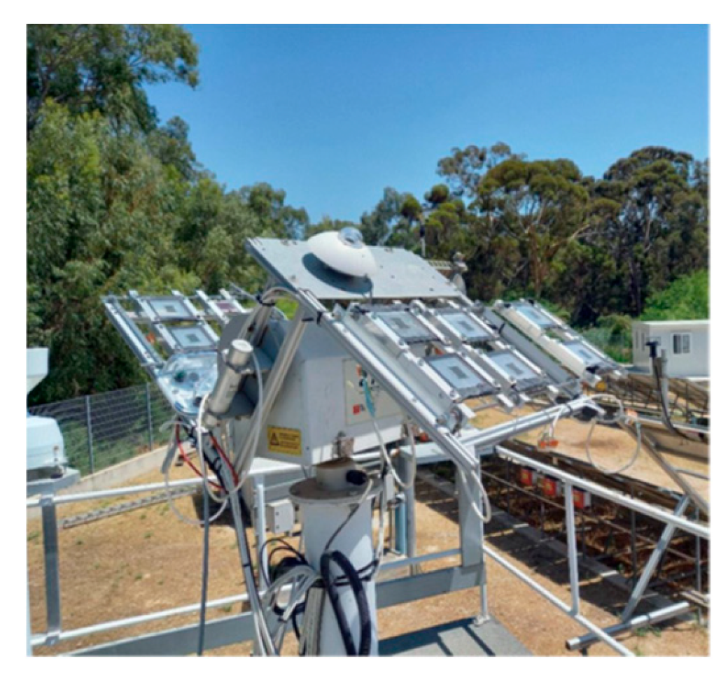
2.3. Outdoor Measurement Systems
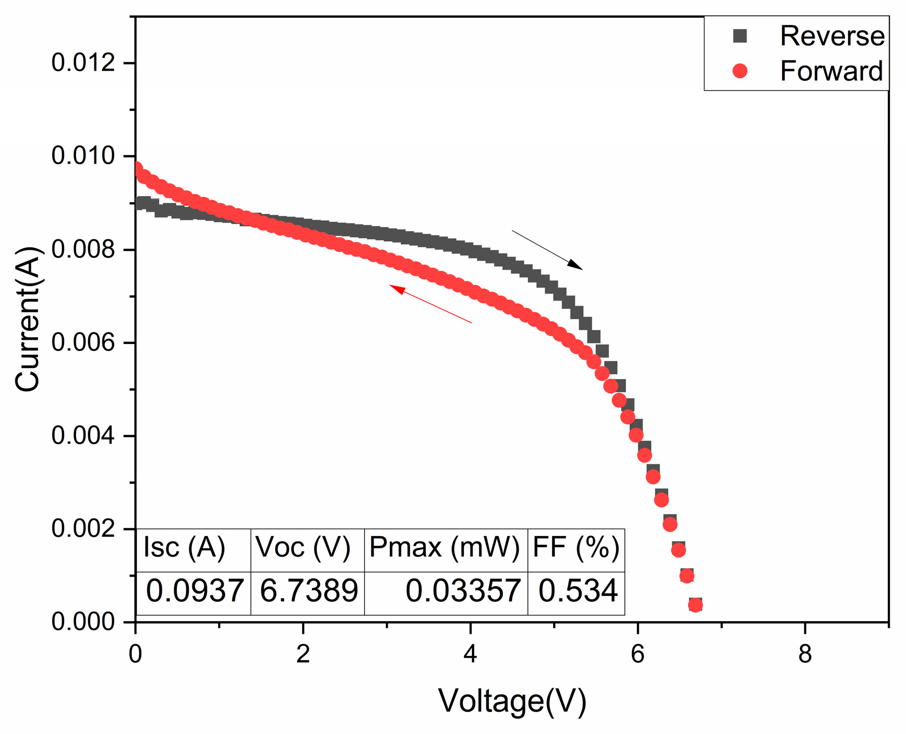
The samples labeled as S5, S6, and S7 were monitored over the period between August 2021 and January 2022 (see Figure 3). During this period, the modules were removed from the field for almost three weeks (in November 2021 and December 2021) for indoor measurements and then located back in the field. The perovskite devices were mounted outdoors in a fixed plane array, and current–voltage (IV) measurements were collected every ten minutes.
Between IV scans, the modules were left at open-circuit voltage (Voc). Both forward (<0 V to >Voc) and reverse (>Voc to <0 V) voltage sweeps were applied to the devices for the IV collection. A forward-first voltage sweep strategy was used in all instances since that was found to minimize hysteresis effects in the samples under test. The voltage sweep rate was chosen to be 1 V/s. The voltage scan rate is a key factor of the hysteresis [21] and should be carefully investigated for each perovskite technology device before field operation. The selection of the sweep rate value was based on taking into consideration indoor studies of perovskite modules at different sweep rates. Indoor studies demonstrated non-significant changes in IV parameters in a range between 0.3 V/s and 2 V/s. Therefore, the IV curves outdoors were set to be acquired as fast as possible (1 V/s) to avoid being affected by any sudden fluctuations in ambient conditions (e.g., irradiance changes due to clouds) that would considerably introduce significant measurement artifacts during our outdoor IV monitoring.
Alongside the IV traces from the devices, environmental sensors were used to collect solar irradiance in the plane of array, ambient and device temperature, wind velocity, and humidity/precipitation levels. The electrical measurements were acquired by a single current–voltage source-meter multiplexed to take sequential measurements from the testing devices. LabVIEW software was designed to record the IV traces every ten minutes at high global normal irradiance (GNI) conditions (GNI > 400 W/m2).

3. Results

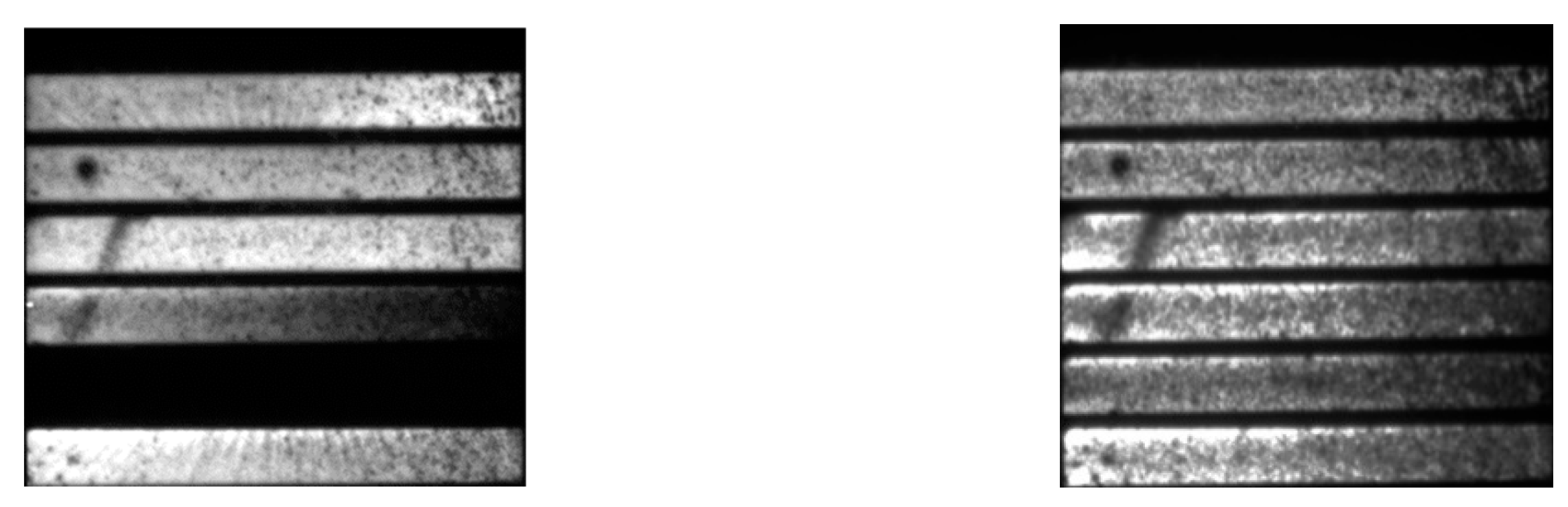
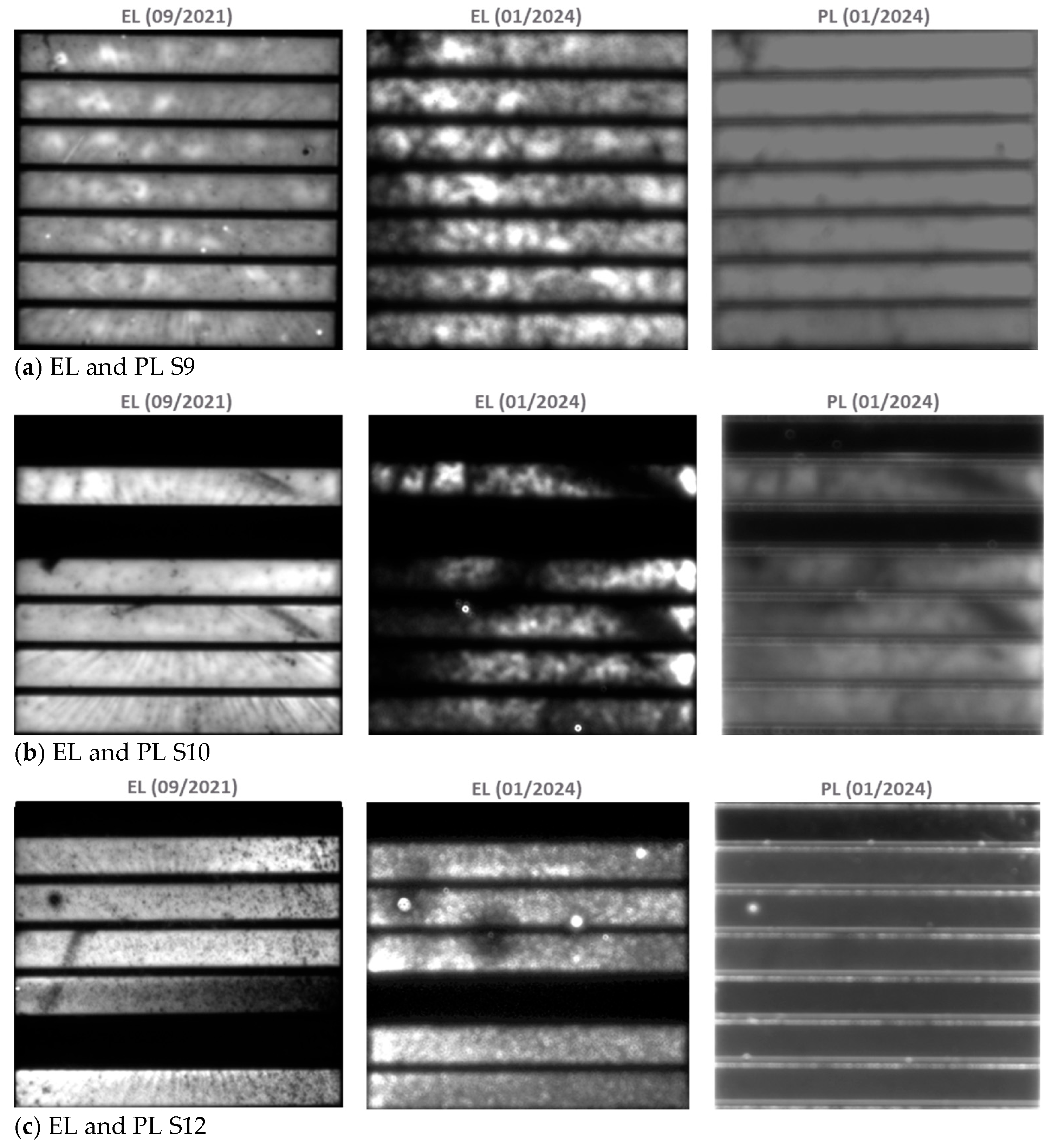
3.1. Perovskite Mini-Modules—Indoor Results

Dark storage studies were performed over a period of three years on perovskite mini-modules according to the ISOS-D protocol [22] to provide information regarding the stability of the perovskites in the absence of light but in the presence of oxygen, moisture, and other atmospheric components naturally present in the air. Four perovskite mini-modules (S9, S10, S11, and S12) were kept indoors at room temperature and measured at regular time intervals with several methods such as EL/PL/DLIT/IV and sometimes Raman spectroscopy. The same methodology was followed for the indoor characterization of the samples to target reliable stability assessment of the mini-modules. The modules were stored in the dark at ambient temperature conditions between measurements. As can be seen in Figure 4, the mini-modules present different trends in their power output evolution over time. The application of the different characterization techniques (EL/PL/DLIT/Raman) during the dark storage of the modules and the impact of several environmental factors (humidity, oxygen, and temperature) have different impacts on the intrinsic stability and the electrical characteristics of each device, and this is the major reason for the different power output evolutions among the perovskite devices. The changes observed in the output power of the devices were found to be sometimes reversible and in other cases irreversible. Mini-module S9 was found not to be affected by any of the characterization techniques applied to the samples over the years. Module S9 was found to be the most stable structure, with a power change of only 15% over almost three years of frequent indoor IV testing. On the other hand, module S11 was affected by Raman spectroscopy measurements in spring 2022 and this led to a power output increase in the sample. Module S10 was found to degrade after the implementation of the same type of measurements in spring 2022.
It is worth noting that the differences between the output power of the samples at the beginning, in 07/21, were caused by some difficulties in device preparation.
The initial electrical characteristics of the mini-modules S9, S10, S11, and S12 were ascertained after their delivery to AIT (see Table 1). Moreover, spatially resolved EL images were collected from the samples to detect the presence of defects and shunts or inactive cells in the devices (see Figure 5). All devices present EL inhomogeneities in their active cells, while in some samples, some cells present no illumination, indicating their inability to produce sufficient radiative recombination even in their pristine state. The spatially resolved EL images of the modules collected after their delivery to AIT are shown in Figure 6.
One important observation arising from the systematic investigation of the spatially resolved EL images is the change in the radiative emission from samples after the implementation of other optical measurements (DLIT, Raman spectroscopy, etc.) on them. A characteristic example is the change in the EL image of module S10 after the DLIT measurements were conducted on the sample (see Figure 6). After DLIT measurements in that sample, an interrupted contact was reactivated, thus resulting in the radiative activation of one cell in the mini-module (after DLIT measurement, there was only one inactive cell instead of two). DLIT measurements might put a great strain on the modules, with the potential to induce degradation, interrupt electrical contact, or even re-establish broken contacts.
The changes in the major electrical parameters of the module before and after the implementation of DLIT measurements can be found in Table 2. A systematic investigation of IV measurements in that specific sample revealed a subsequent return of the power values to those that existed before DLIT measurements (see Table 3).
After the performance of some optical measurements in April 2022, mini-module S10 was completely degraded (see Figure 6).
Changes in the power output after Raman measurements were detected in mini-module S11. A power increase was obtained after Raman testing in the sample between February and April 2022 (see Figure 4), indicating that the output characteristics of the perovskites are sensitive to electrical and optical measurements due to their metastable behavior.

Systematic EL and PL Measurements of Control Samples

EL measurements of mini-modules S9, S10, and S12 were implemented in September 2021 and February 2024 to reveal the changes in shunt/defect evolutions in the samples. The results are shown in Figure 6. It is worth noting that the same voltage was applied to the samples during EL testing on both dates (September 2021 and February 2024). Additionally, PL measurements (with green LEDs: 500–570 nm) were performed (see Figure 6).
EL images after three years of dark storage demonstrate lower emissions and more inhomogeneities within the modules. In mini-modules S9 and S10, the reduction in radiative emission is more pronounced at the edges of the modules. The power measurements over the three years (see Figure 4) show a slight decrease in power and an increase in series resistance. Significant differences in stability among different samples were identified. The lack of stability of perovskite materials is a well-known issue [23], and it has been shown that, at the device level, several degradations occur simultaneously at various interfaces. Moisture, UV light, hot temperatures, and exposure to the outside air can all directly contribute to these degradations. The causes of the stability issue can thus be determined to be intrinsic stability, moisture ingress, oxygen ingress, and illumination-accelerated decomposition [24]. Intrinsic stability refers to the chemical and structural stability of devices throughout a wide range of photovoltaic working conditions in the presence of contaminants, particularly oxygen and water, which were introduced into the device during production. Extrinsic stability is concerned with the failures of sealing and moisture-blocking layers. Under normal conditions, degradation mechanisms are activated or accelerated. The aforementioned conditions may also contribute to the material’s disintegration of the organic layer, top electrode instability, photo-degradation, and crystallization instability. Numerous degradations can begin even in the absence of water or oxygen due to the intrinsic deterioration produced by thermal stress or illumination. Both the employed charged transport material’s instability and the inherent instability of the perovskite material are to blame for the stability drawbacks [25].

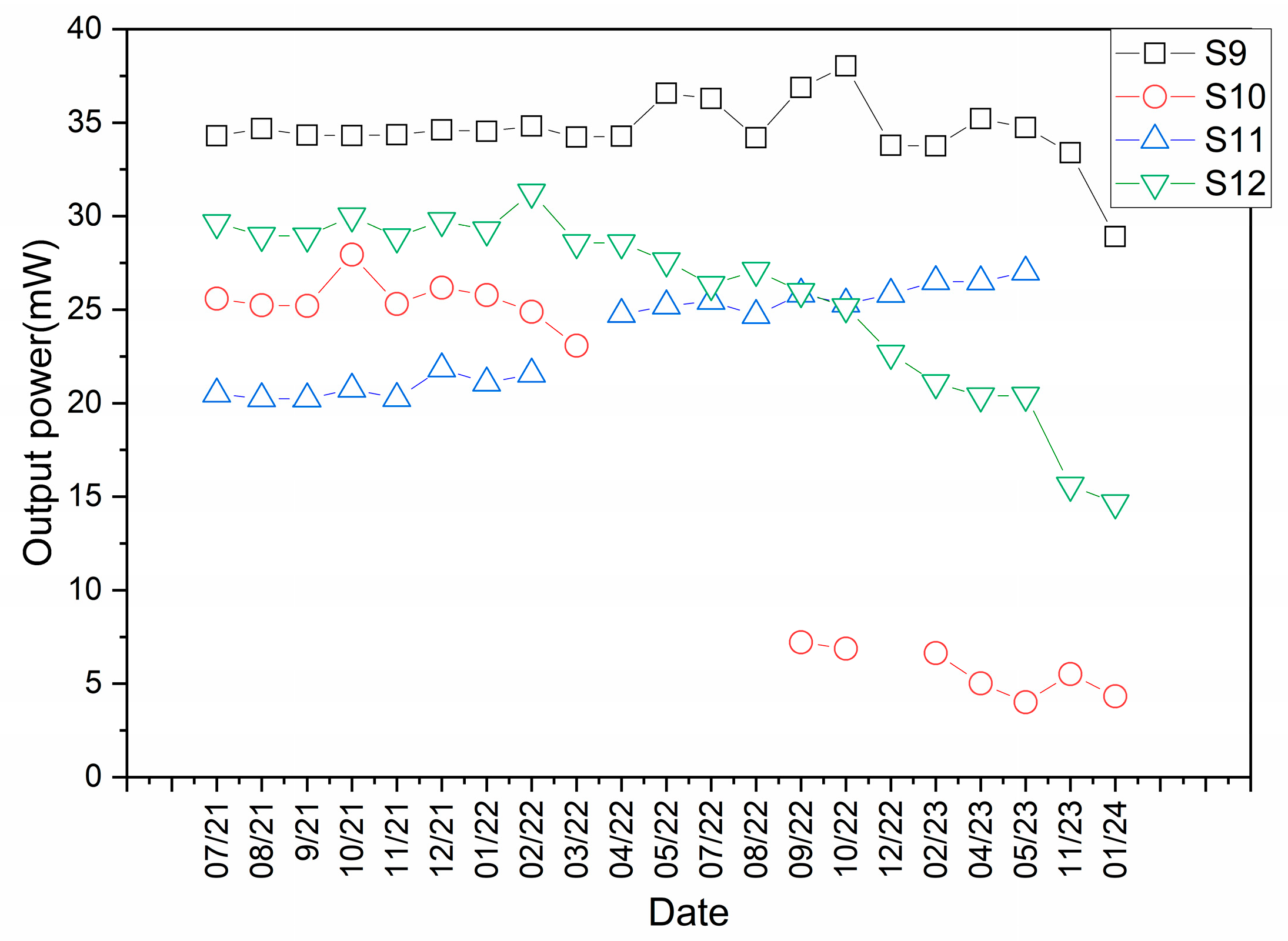
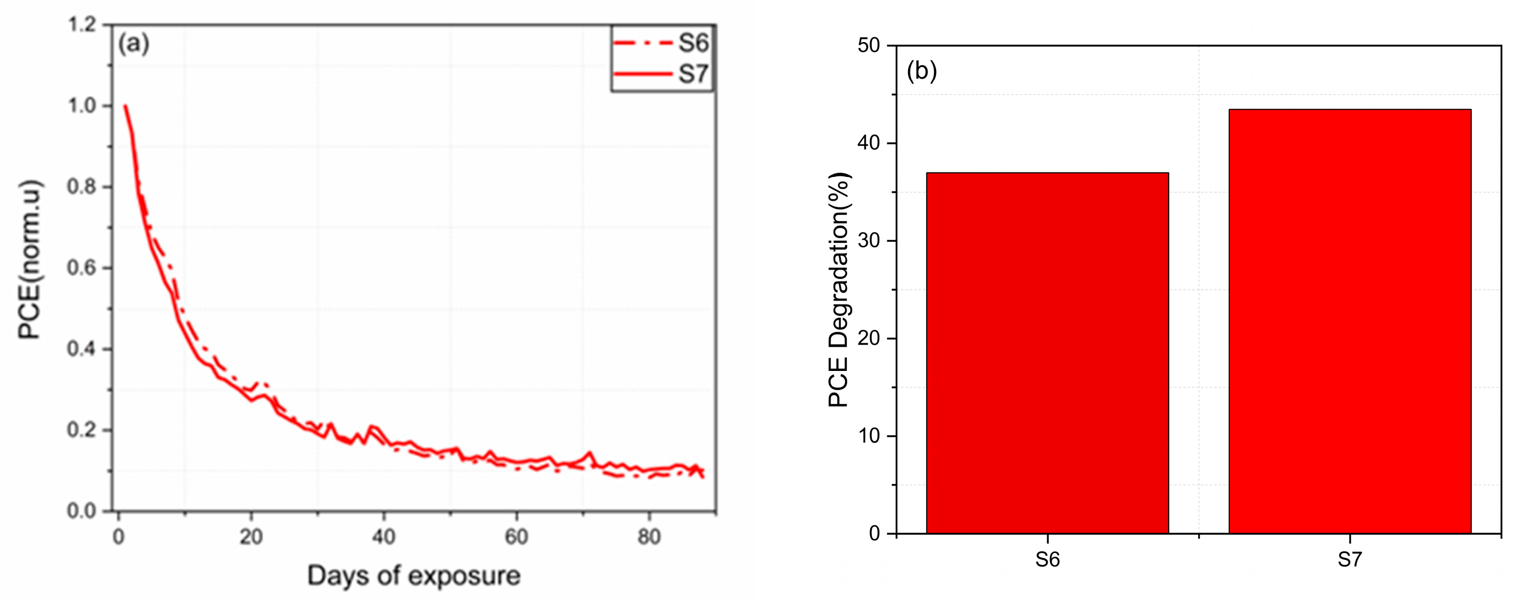
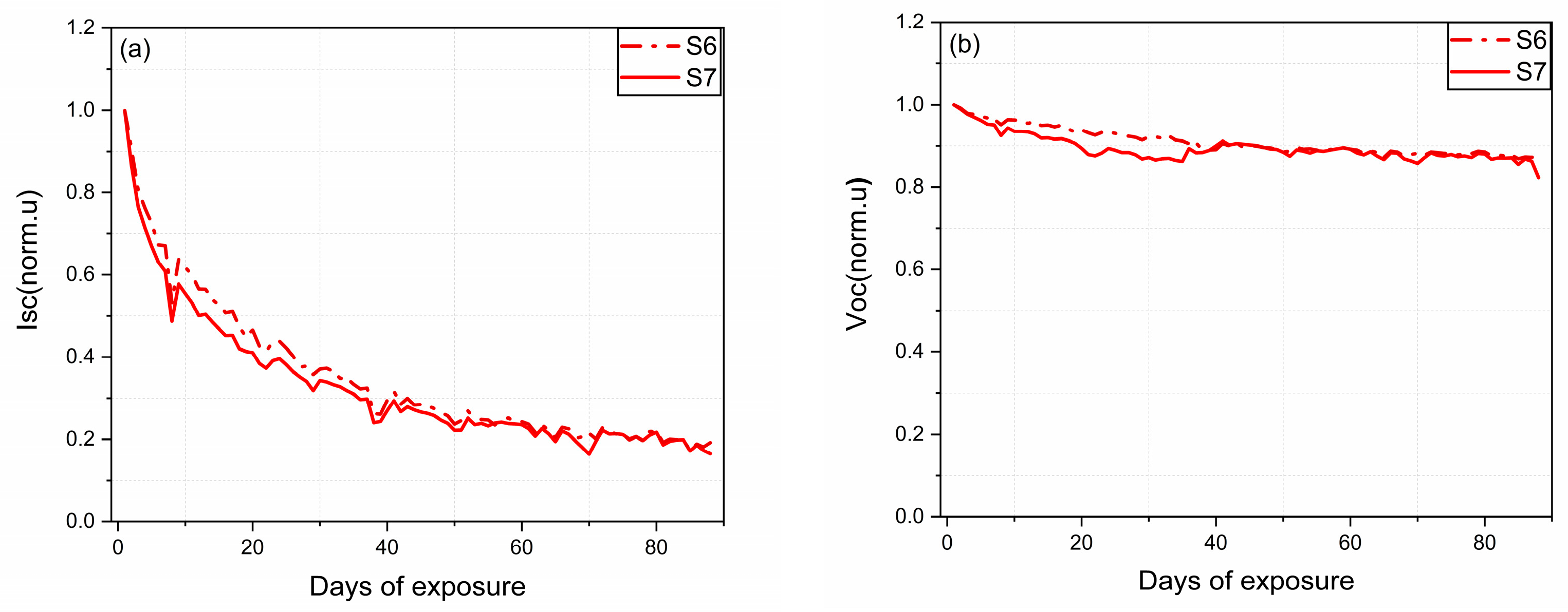
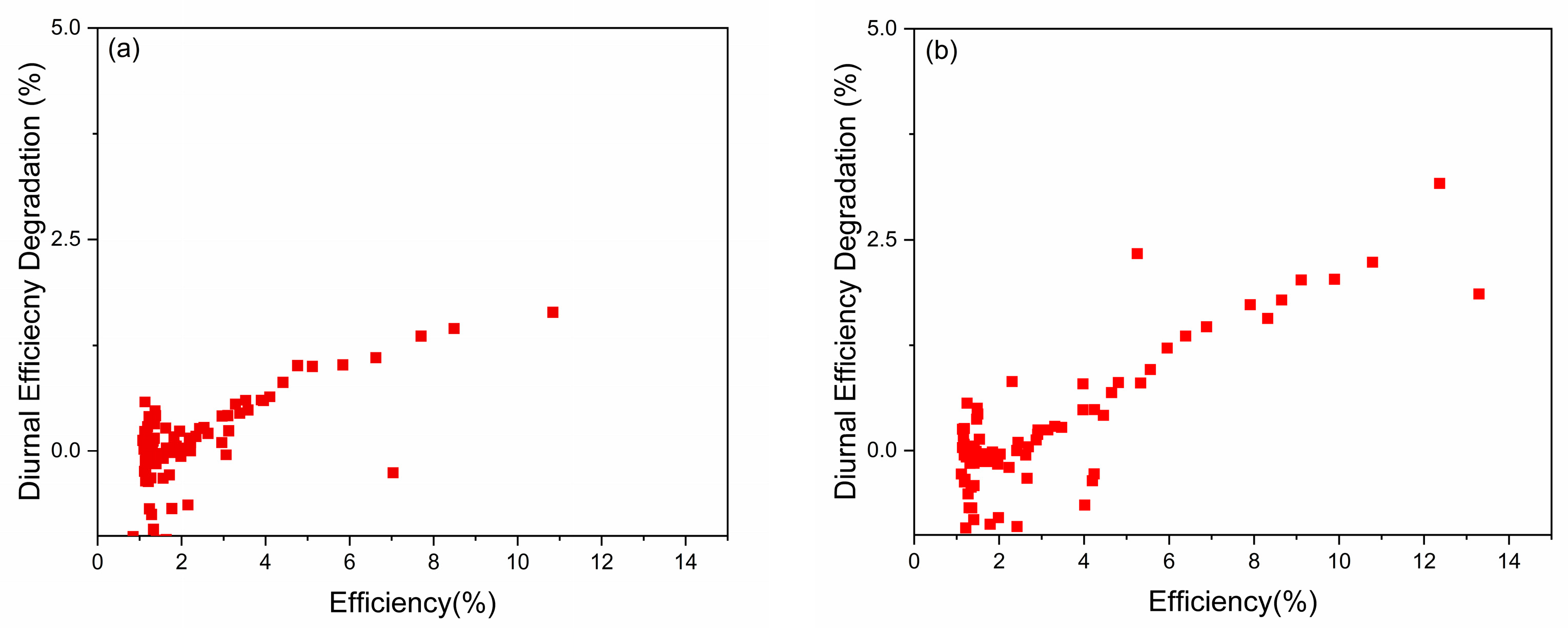
3.2. Outdoor Testing Results of the Mini-Modules

All modules exposed outdoors presented a rapid drop in performance (see Figure 7a) during the first days of exposure. The mean value of efficiency on the first day of exposure was set as the starting point for the normalization in Figure 7a. Perovskite mini-modules presented a continuous and significant drop in their efficiency until it stabilized after the 60th day of exposure. The initial decay of the performance efficiency in perovskite devices is known as “burn-in” degradation [26], and previous reports demonstrated that this is closely related to the current extraction, non-radiative recombination, and charge transport processes [27].
For a better understanding of the performance degradation of the modules over the first days of outdoor exposure, the power conversion efficiency loss was calculated for each module over the first week of testing. The graph in Figure 7b demonstrates that the modules presented a reduction in efficiency up to 45% of their initial values during the first week of testing. During this period, the mean module temperature was around 49.6 °C, and the total weekly solar irradiation received by the modules was 41.25 kWh/m2. This module temperature measurement was collected only during the collection of current–voltage characteristics of the modules at irradiance values higher than 400 W/m2.
It is worth noting that no visible degradation due to humidity ingress inside the encapsulant material was observed in any modules under testing. A typical example of the IV curves presented during the first days of testing (at early degradation stages) is demonstrated in Figure 8.
To identify the root cause of the efficiency degradation of the modules, the electrical parameters of the modules were studied over the testing period. The evolution of short-circuit and open-circuit voltage over the 23 weeks of outdoor operation is depicted in Figure 9. The decrease in power conversion efficiency of the modules is linked to a significant reduction in current output. The perovskite mini-modules present a current exponential reduction from their first day of operation outdoors. A current reduction of 50% occurs in perovskite devices in only 14 days of outdoor testing. Voltage losses were much lower than current losses in all modules tested outdoors.
The modules were uninstalled from the field on the 23rd of November (day 91) and then located back on the 10th of December (day 108). A significant performance recovery occurred in the mini-modules during their storage in the dark, and thus higher performance was detected after their installation in the field on day 108. To examine the root cause of performance recovery, the short-circuit and open-circuit voltage recovery were calculated. The short-circuit recovery in modules S6 and S7 was found to be 6.2% and 6.8%, respectively, while the open-circuit recovery was found to be much lower (1.0% and 0.7%). The results provide an indication that current is the major origin of performance recovery in the modules under testing, and this is related to the ion migration and charge redistribution in the material in the dark.
The efficiency of the perovskite modules changes over the course of a day. The diurnal efficiency degradation of the modules under test was calculated for each day in the field to investigate any possible trend with efficiency value. The diurnal efficiency degradation was calculated based on the efficiency values at the beginning and the end of each day at the same irradiation conditions (400 W/m2). The values were normalized to the initial efficiency value to have comparable results. More details regarding this approach can be found in the diurnal efficiency degradation versus efficiency for the samples exposed outdoors graph, which can be found in Figure 10. Diurnal performance degradation values of up to 2.5% were found over the timespan of the outdoor studies. High diurnal efficiency degradation is detected at higher efficiency values in modules tested outdoors, and a linear relationship is present between those quantities. Accelerated performance degradation occurs in modules from the first days of exposure, leaving the modules with low overall efficiency after some days of testing, which show lower diurnal changes in efficiency.
The hysteresis index was then calculated to study any correlation of hysteresis with the degradation stage. The hysteresis index was introduced in previous papers for quantifying hysteresis in perovskite solar cells [28]. Previous works reported that hysteresis is due to the interaction of the mobile ionic species with the external bias, which can affect the built-in field and modify the energetic environment of the interfaces [29]. For a more precise analysis of the results, the hourly dependence of the electrical characteristics was studied, and the data were separated into morning and evening acquisition. The morning hours correspond to the data collected until 12 p.m. noon while the evening hours correspond to the data collected after 12 p.m. noon. The evolution of the hysteresis index at different months of testing is depicted in Figure 11.
Figure 11 demonstrates a significant increase in hysteresis during the second month of testing in both samples investigated outdoors due to the significant increase in defect and ion accumulation in the devices. The increase in hysteresis index is present during the third month (M3) in module S7. However, this is not obtained in module S6 for unclarified reasons. Both samples present a significant decrease in the hysteresis index in the fourth month (M4) of testing, which is the month after the samples were kept indoors for two weeks. This might be attributed to the self-healing of the light-activated trap states in the dark that act as ion accumulation centers [30]. The hysteresis index is then returned to higher values at month 5 due to the formation of light-activated trap states after some time of light soaking outdoors. It is worth noting that a larger deviation of the hysteresis index values occurs during the first month of testing due to the significant performance degradation that occurs that month and consequently larger changes in the hysteresis index.
One important observation arising from Figure 11 is the presence of a negative hysteresis index in some cases. Negative capacitance and inverted hysteresis effects in perovskite devices have been reported before [31]. In an attempt to find the origin of the negative hysteresis index in the perovskite mini-modules, all the instances of negative hysteresis were gathered alongside the environmental conditions presented during those cases. The negative hysteresis index instances were found to be attributed to rapid and significant changes in irradiance levels during the IV collection, resulting in an overestimation of the forward sweep of the IV curve over the reverse sweep.
The environmental conditions present over the testing period of outdoor exposure were recorded at regular time intervals. Particularly, data such as global normal irradiance (GNI), ambient temperature, and relative humidity were acquired every 5 min. The total irradiation received by the devices over time and the average ambient temperature present during the outdoor exposure of the two batches are plotted in Figure 12.

4. Conclusions

In this work, both indoor optoelectronic characterization methods and investigations of outdoor stability were employed to understand the degradation of perovskite cells and mini-modules. Initial defects and shunts were identified by EL, PL, and IV measurements, and it turned out that significant differences in degradation occured in perovskites tested indoors and outdoors. Indoor studies revealed that the degradation is much lower than assumed. These are very good results, which predict a successful future for the use of perovskites. It should be noted that some indoor measurements (DLIT and Raman) led to an increase or decrease in power, partly reversible but also irreversible. Thus, perovskites are very sensitive to some optical measurements. Concerning outdoor measurements, the defect and shunt evolutions were obtained with the degradation stage. Performance reduction of up to 45% was observed in perovskite devices tested outdoors. The diurnal performance degradation of the perovskite devices tested outdoors was found to be higher at early degradation stages, while changes in the hysteresis index were obtained with light soaking outdoors and dark storage in the dark. The higher irradiation and ambient temperature present during summer months were found to cause accelerated efficiency degradation in the modules. This fact provides evidence that module lifetime depends on the temperature and irradiance levels during the first days of testing and that their values are critical for the perovskite module operation.
Further indoor tests and outdoor tests of differently structured perovskite samples and perovskite tandem cells need to be performed to identify more defects and thus be able to improve the perovskite cell and module structure.

Author Contributions

Conceptualization, A.A.; Validation, M.H. and T.A.; Writing—original draft, R.E.; Writing—Review & Editing, V.P.; Sample Preparation, A.H. and A.A.; Interpretation of Data, R.E.; Analysis, A.M., G.U. and V.P.; Supervision, G.E.G. and T.A.; Review, M.H. and T.A. All authors have read and agreed to the published version of the manuscript.

Funding

This work was funded by the European Union through the TESTARE project (Grant ID: 101079488) and by the European Regional Development Fund and the Republic of Cyprus through the DegradationLab project (Grant ID: INFRASTRUCTURES/1216/0043, and through the ViperLab project which has received funding from the European Union’s Horizon 2020 research and innovation program under grant agreement N°101006715.

Data Availability Statement

The original contributions presented in the study are included in the article, further inquiries can be directed to the corresponding author.

Conflicts of Interest

Authors R. Ebner, A. Mittal and G. Ujvari were employed by the research company AIT Austrian Institute of Technology GmbH. Author A. Aguirre and T. Aernouts were employed by the company imec. The remaining authors declare that the research was conducted in the absence of any commercial or financial relationships that could be construed as a potential conflict of interest.

References

  1. NREL. Best Research-Cell Efficiency Chart. Available online: https://www.nrel.gov/pv/cell-efficiency.html (accessed on 3 July 2024).
  2. Li, N.; Niu, X.; Chen, Q.; Zhou, H. Towards commercialization: The operational stability of perovskite solar cells. Chem. Soc. Rev. 2020, 49, 8235–8286. [Google Scholar] [CrossRef] [PubMed]
  3. Baumann, F.; Raga, S.R.; Lira-Cantú, M. Monitoring the stability and degradation mechanisms of perovskite solar cells by in situ and perando characterization. APL Energy 2023, 1, 011501. [Google Scholar] [CrossRef]
  4. Wagner, L.; Bogachuk, D.; Qui, C.; Mathiazhagan, G.; Zouhair, S.; Hinsch, A. Characterization Methods and Technologies for Halide Perovskite Materials and Devices; Wiley-VCH: Weinheim, Baden-Wurttemberg, Germany, 2023; Chapter 2. [Google Scholar] [CrossRef]
  5. Manser, J.S.; Kamat, P.V. Band filling with free charge carriers in organometal halide perovskites. Nat. Photonics 2014, 8, 737–743. [Google Scholar] [CrossRef]
  6. Schubert, M.C.; Mundt, L.E.; Walter, D.; Fell, A.; Glunz, S.W. Spatially Resolved Performance Analysis for Perovskite Solar Cells. Adv. Energy Mater. 2020, 10, 1904001. [Google Scholar] [CrossRef]
  7. Hepp, J.; Machui, F.; Egelhaaf, H.; Brabec, C.J.; Vetter, A. Automatized analysis of IR-images of photovoltaic modules and its use for quality control of solar cells. Energy Sci. Eng. 2016, 4, 363–371. [Google Scholar] [CrossRef]
  8. Mundt, L.E.; Kwapil, W.; Yakoob, M.A.; Herterich, J.P.; Kohlstadt, M.; Wurfel, U.; Schubert, M.C.; Glunz, S.W. Quantitative Local Loss Analysis of Blade-Coated Perovskite Solar Cells. IEEE J. Photovolt. 2019, 9, 452–459. [Google Scholar] [CrossRef]
  9. Rakocevic, L.; Mundt, L.E.; Gehlhaar, R.; Merckx, T.; Aernouts, T.; Schubert, M.C.; Glunz, S.W.; Poortmans, J. Loss Analysis in Perovskite Photovoltaic Modules. Sol. RRL 2019, 3, 1900338. [Google Scholar] [CrossRef]
  10. Jošt, M.; Lipovšek, B.; Glažar, B.; Al-Ashouri, A.; Brecl, K.; Matič, G.; Magomedov, A.; Getautis, V.; Topič, M.; Albrecht, S. Perovskite Solar Cells go Outdoors: Field Testing and Temperature Effects on Energy Yield. Adv. Energy Mater. 2020, 10, 2000454. [Google Scholar] [CrossRef]
  11. Emery, Q.; Remec, M.; Paramasivam, G.; Janke, S.; Dagar, J.; Ulbrich, C.; Schlatmann, R.; Stannowski, B.; Unger, E.; Khenkin, M. Encapsulation and Outdoor Testing of Perovskite Solar Cells: Comparing Industrially Relevant Process with a Simplified Lab Procedure. ACS Appl. Mater. Interfaces 2022, 14, 5159–5167. [Google Scholar] [CrossRef] [PubMed]
  12. Velilla, E.; Jaramillo, F.; Mora-Seró, I. High-throughput analysis of the ideality factor to evaluate the outdoor performance of perovskite solar minimodules. Nat. Energy 2021, 6, 54–62. [Google Scholar] [CrossRef]
  13. Stoichkov, V.; Bristow, N.; Troughton, J.; De Rossi, F.; Watson, T.; Kettle, J. Outdoor performance monitoring of perovskite solar cell mini-modules: Diurnal performance, observance of reversible degradation and variation with climatic performance. Sol. Energy 2018, 170, 549–556. [Google Scholar] [CrossRef]
  14. Manshanden, P.; Coletti, G.; Ronchetti, M.W.; Jansen, M.J.; Rosca, V.; Späth, M.; Zardetto, V.; Verhees, W.J.H.; Dogan, I.; Fledderus, H.; et al. Prediting Outdoor Performance of Perovskite Modules with Modified Reliability Testing; EU PCSEC: Vienna, Austria, 2023. [Google Scholar] [CrossRef]
  15. Ali, M.U.; Mo, H.; Li, Y.; Djurišić, A.B. Outdoor stability testing of perovskite solar cells: Necessary step toward real-life applications. APL Energy 2023, 1, 020903. [Google Scholar] [CrossRef]
  16. Li, J.; Dagar, J.; Shargaieva, O.; Maus, O.; Remec, M.; Emery, Q.; Khenkin, M.; Ulbrich, C.; Akhundova, F.; Márquez, J.A.; et al. Ink Design Enabling Slot-Die Coated Perovskite Solar Cells with >22% Power Conversion Efficiency, Micro-Modules, and 1 Year of Outdoor Performance Evaluation. Adv. Energy Mater. 2023, 13, 2203898. [Google Scholar] [CrossRef]
  17. Chen, W.; Han, B.; Hu, Q.; Gu, M.; Zhu, Y.; Yang, W.; Zhou, Y.; Luo, D.; Liu, F.-Z.; Cheng, R.; et al. Interfacial stabilization for inverted perovskite solar cells with long-term stability. Sci. Bull. 2021, 66, 991–1002. [Google Scholar] [CrossRef] [PubMed]
  18. Ramirez, D.; Velilla, E.; Montoya, J.F.; Jaramillo, F. Mitigating scalability issues of perovskite photovoltaic technology through a p-i-n meso-superstructured solar cell architecture. Sol. Energy Mater. Sol. Cells 2019, 195, 191–197. [Google Scholar] [CrossRef]
  19. De Bastiani, M.; Van Kerschaver, E.; Jeangros, Q.; Rehman, A.U.; Aydin, E.; Isikgor, F.H.; Mirabelli, A.J.; Babics, M.; Liu, J.; Zhumagali, S.; et al. Toward Stable Monolithic Perovskite/Silicon Tandem Photovoltaics: A Six-Month Outdoor Performance Study in a Hot and Humid Climate. ACS Energy Lett. 2021, 6, 2944–2951. [Google Scholar] [CrossRef]
  20. Liu, J.; Aydin, E.; Yin, J.; De Bastiani, M.; Isikgor, F.H.; Rehman, A.U.; Yengel, E.; Ugur, E.; Harrison, G.T.; Wang, M.; et al. 28.2%-efficient, outdoor-stable perovskite/silicon tandem solar cell. Joule 2021, 5, 3169–3186. [Google Scholar] [CrossRef]
  21. Balaguera, E.H.; Bisquert, J. Accelerating the Assessment of Hysteresis in Perovskite Solar Cells. ACS Energy Lett. 2024, 9, 478–486. [Google Scholar] [CrossRef] [PubMed]
  22. Khenkin, M.V.; Katz, E.A.; Abate, A.; Bardizza, G.; Berry, J.J.; Brabec, C.; Brunetti, F.; Bulović, V.; Burlingame, Q.; Di Carlo, A.; et al. Consensus statement for stability assessment and reporting for perovskite photovoltaics based on ISOS procedures. Nat. Energy 2020, 5, 35–49. [Google Scholar] [CrossRef]
  23. Chowdhury, T.A.; Bin Zafar, A.; Islam, S.-U.; Shahinuzzaman, M.; Islam, M.A.; Khandaker, M.U. Stability of perovskite solar cells: Issues and prospects. RSC Adv. 2023, 13, 1787–1810. [Google Scholar] [CrossRef] [PubMed]
  24. Bryant, D.; Aristidou, N.; Pont, S.; Sanchez-Molina, I.; Chotchunangatchaval, T.; Wheeler, S.; Durrant, J.R.; Haque, S.A. Light and oxygen induced degradation limits the operational stability of methylammonium lead triiodide perovskite solar cells. Energy Environ. Sci. 2016, 9, 1655–1660. [Google Scholar] [CrossRef]
  25. Li, W.; Zhang, W.; Van Reenen, S.; Sutton, R.J.; Fan, J.; Haghighirad, A.A.; Johnston, M.B.; Wang, L.; Snaith, H.J. Enhanced UV-light stability of planar heterojunction perovskite solar cells with caesium bromide interface modification. Energy Environ. Sci. 2016, 9, 490–498. [Google Scholar] [CrossRef]
  26. Ding, C.; Yin, L.; Wang, J.; Larini, V.; Zhang, L.; Huang, R.; Nyman, M.; Zhao, L.; Zhao, C.; Li, W.; et al. Boosting Perovskite Solar Cells Efficiency and Stability: Interfacial Passivation of Crosslinked Fullerene Eliminates the “Burn-in” Decay. Adv. Mater. 2023, 35, 2207656. [Google Scholar] [CrossRef] [PubMed]
  27. Duan, L.; Zhang, Y.; He, M.; Deng, R.; Yi, H.; Wei, Q.; Zou, Y.; Uddin, A. Burn-In Degradation Mechanism Identified for Small Molecular Acceptor-Based High-Efficiency Nonfullerene Organic Solar Cells. ACS Appl. Mater. Interfaces 2020, 12, 27433–27442. [Google Scholar] [CrossRef] [PubMed]
  28. Habisreutinger, S.N.; Noel, N.K.; Snaith, H.J. Hysteresis Index: A Figure without Merit for Quantifying Hysteresis in Perovskite Solar Cells. ACS Energy Lett. 2018, 3, 2472–2476. [Google Scholar] [CrossRef]
  29. Tress, W. Metal Halide Perovskites as Mixed Electronic–Ionic Conductors: Challenges and Opportunities—From Hysteresis to Memristivity. J. Phys. Chem. Lett. 2017, 8, 3106–3114. [Google Scholar] [CrossRef] [PubMed]
  30. Nie, W.; Blancon, J.-C.; Neukirch, A.J.; Appavoo, K.; Tsai, H.; Chhowalla, M.; Alam, M.A.; Sfeir, M.Y.; Katan, C.; Even, J.; et al. Light-activated photocurrent degradation and self-healing in perovskite solar cells. Nat. Commun. 2016, 7, 11574. [Google Scholar] [CrossRef] [PubMed]
  31. Alvarez, A.O.; Arcas, R.; Aranda, C.A.; Bethencourt, L.; Mas-Marzá, E.; Saliba, M.; Fabregat-Santiago, F. Negative Capacitance and Inverted Hysteresis: Matching Features in Perovskite Solar Cells. J. Phys. Chem. Lett. 2020, 11, 8417–8423. [Google Scholar] [CrossRef] [PubMed]
Figure 1. (a) PIN structure of each sub-cell. (b) Cross-section of mini-module.
Inorganics 12 00219 g001
Figure 2. Perovskite mini-module: front side (left) and back side (right).
Inorganics 12 00219 g002
Figure 3. Perovskite mini-modules located outdoors and tested side by side.
Inorganics 12 00219 g003
Figure 4. Aging behavior of the perovskite mini-modules.
Inorganics 12 00219 g004
Figure 5. Spatially resolved EL images of mini-module “S10” before (left) and after (right) DLIT measurements in October 2021.
Inorganics 12 00219 g005
Figure 6. Spatially resolved EL images in September 2021 (left) and January 2024 (right) in mini-modules (a) S9, (b) S10, and (c) S12.
Inorganics 12 00219 g006
Figure 7. Efficiency degradation of modules (a) against time of exposure and (b) after one week of outdoor testing.
Inorganics 12 00219 g007
Figure 8. A typical example of IV curves collected from perovskite mini-module S7. At each instant, forward and reverse scan sweeps are collected. The IV curves correspond to the 2nd day of outdoor testing (27 August 2021, 10:33 a.m.). Forward curve was implemented first (black arrow) and then reverse curve (red arrow).
Inorganics 12 00219 g008
Figure 9. (a) Short-circuit current and (b) open-circuit voltage evolution over time for the perovskite mini-modules under testing.
Inorganics 12 00219 g009
Figure 10. Diurnal performance degradation versus efficiency values for mini-modules (a) S6 and (b) S7.
Inorganics 12 00219 g010
Figure 11. The hysteresis index at different months of outdoor exposure for modules (a) S6 and (b) S7. The data are separated into morning (before 12 a.m.) and evening acquisition (after 12 a.m.) for more detailed analysis.
Inorganics 12 00219 g011
Figure 12. (a) Total irradiation received by the modules over time and (b) the mean ambient temperature at different days of exposure.
Inorganics 12 00219 g012
Table 1. Initial IV measurement results of the mini-modules S9, 10, 11, and 12 (measurement uncertainty is ±5.31% of PMPP, ±3.08% of ISC, ±3.02% of VOC, and ±3.1% of FF) caused by the metastable behavior of perovskites and the high capacitive effects).
ISC
[mA]
VOC
[V]
FF
[%]
PMPP [mW]Jsc [mA/cm2]
S910.267.78942.9134.2913.10
S1010.566.10639.7025.5913.48
S1110.375.26037.6020.5013.24
S1210.446.99340.6029.6413.33
Table 2. IV measurement results of the mini-module “S10” before and after DLIT measurement (10/21).
Mini-ModuleISC [mA]VOC [V]FF [%]PMPP [mW]Jsc [mA/cm2]
S1010.566.10639.7025.5913.48
S10 DLIT10.396.75639.8127.9413.27
Table 3. IV measurements on “S10”.
Mini-ModuleISC [mA]VOC [V]FF [%]PMPP [mW]Jsc [mA/cm2]
S10 initial value10.566.10639.7025.5913.48
S10 DLIT October 202110.396.75639.8127.9413.27
S10 November 202110.486.74838.1826.9913.38
S10 December 202110.416.73737.3126.1813.30
S10 January 202210.436.76436.9525.7813.17
S10 February 202210.456.84334.8024.8913.35
S10 March 202210.386.39734.7323.0713.26
Disclaimer/Publisher’s Note: The statements, opinions and data contained in all publications are solely those of the individual author(s) and contributor(s) and not of MDPI and/or the editor(s). MDPI and/or the editor(s) disclaim responsibility for any injury to people or property resulting from any ideas, methods, instructions or products referred to in the content.

