Article

The Influence of Annealing Temperature on the Microstructure and Electrical Properties of Sputtered ZnO Thin Films

Department of Physics, College of Science, King Faisal University, P.O. Box 400, Al Ahsa 31982, Saudi Arabia
Inorganics 2024, 12(9), 236; https://doi.org/10.3390/inorganics12090236
Submission received: 21 July 2024 / Revised: 18 August 2024 / Accepted: 26 August 2024 / Published: 29 August 2024
(This article belongs to the Special Issue New Advances into Nanostructured Oxides, 2nd Edition)

Abstract

:
Thin films are the backbone of the electronics industry, and their widespread application in heat sensors, solar cells, and thin-film transistors has attracted the attention of researchers. The current study involves the deposition of a hetero-structured (ZnO/Zn/ZnO) thin film on a well-cleaned glass substrate using the DC magnetron sputtering technique. The samples were then annealed at 100, 200, 300, 400, and 500 °C. The structural, morphological, and electrical characteristics of the annealed samples as well as one as-deposited sample were then examined using atomic force microscopy (AFM), scanning electron microscopy (SEM), X-ray diffraction (XRD), and a Hall effect measuring apparatus. XRD analysis showed a hexagonal ZnO crystal structure for the samples annealed at 300 and 400 °C, whereas the samples annealed at 100 and 200 °C showed metallic zinc and hexagonal ZnO, and the crystallinity decreased for the sample annealed at 500 °C with pure hexagonal crystal symmetry. According to the AFM study, as the annealing temperature increases, the average roughness (Ra) decreases. Temperature has an inverse relationship with particle size. The optimal annealing temperature was determined to be 400 °C. Over this temperature range, the average roughness and particle size increased. Similarly, when Ra decreased, the conductivity increased and the resistance decreased. A fundamental difficulty is that the heating of the heterostructure to 400 °C melts the Zn-based intermediate layer, which alters the Zn phase and disrupts the sample homogeneity.

1. Introduction

Semiconductor nanomaterials play a significant role in renewable energy, notably in thin-film solar cells, and have attracted the attention of scientists and researchers worldwide [1]. Many elemental and compound semiconductor nanomaterials have been investigated, with ZnO being one of the most prominent and promising [2]. ZnO is a binary II–VI compound semiconductor material having Wurtzite crystal structure, a wide and direct bandgap of 3.3 eV at ambient temperature, and an exciton binding energy of 60 meV [3,4,5]. It can be grown in several different types of nanoscales, thus making it possible to obtain various novel products [6]. Moreover, the properties of ZnO can be altered by fabricating thin films [7]. ZnO thin films have been extensively researched in various areas due to their high bond strength [8], good optical performance [9], severe exciton stabilisation [10], and outstanding piezoelectric properties [11], and they have many prospective applications in multiple technological areas, such as clear film/electrodes [12] in screen systems and solar energy [13]. Another benefit of ZnO compared to other metals is its substantial cost, which makes it an extremely prospective candidate for industrial applications [14]. ZnO is currently one of the leading materials used as a window layer [9], transparent conducting oxide (TCO) [15,16], and buffer layer in the solar cell industry [17].
The transparent conductive oxides (TCOs) thin films have several options in optoelectronic devices. Such thin films can be used especially for organic light-emitting diodes (OLEDs) [16], solar cells, heat sensors [18,19], and thin-film transistors (TFTs) [20]. One of the most studied and industrially used TCO is tin-doped indium oxide (ITO) [17,21]. The latest rise in consumption by the optoelectronic devices sector ITO has become rare and more expensive [6,22]. Because of its advantages in several fields and its unique characteristics like low price, non-toxicity, and good chemical stability in maintaining plasma, an extremely successful substitute for indium tin oxide (ITO) is ZnO [21,23]. Native and extrinsic defects in ZnO nanostructures, however, are considered to reach profound concentrations that limit their application performance [24]. A detailed understanding of the type, composition, and electronic parameters of deep-level facilities is the key to understanding and controlling electronic characteristics [7,25]. Understanding surface defect behaviour is essential for ZnO to be successfully applied [26]. Inherent defects and vacancies in ZnO are mainly classified into four kinds: surface defects including O vacancies (VO) and Zn vacancies (VZn) and interstitials (Zn and O), which are part of the majority of the fabric [27,28]. ZnO’s large-scale development process regulates the development of its inherent flaws [29,30]. It is recognized that the number of failures depends on a post-growth sample therapy, which can change its characteristics significantly [31,32]. However, in many practical systems, no control over defects is one of the major problems in using ZnO [33,34]. Thus, one way to control point and surface defects is to post-anneal the ZnO nanoparticles to obtain high UV photodetection in a short interval of time [26,32]. Higher temperature treatment in air and N2 results in excellent monitoring of surface-related abnormalities such as VO and VZn and decreases radiative recombination of the surface defects [22,35]. To achieve a defect-free ZnO thin film, we used the magnetron sputtering method to deposit thin film at room temperature with a ZnO/Zn/ZnO heterostructure accompanied by thermal annealing at various temperatures. The objective of the ZnO/Zn/ZnO heterostructure was to obtain a defect-free ZnO thin film by harnessing the characteristics of the intermediate Zn layer. The metallic Zn layer exhibits a ‘surfactant effect’, promoting recrystallization during the deposition process. In conjunction with moderate-temperature annealing, the Zn layer facilitates the ‘therapy’ of surrounding ZnO crystallites, enhancing the overall crystalline quality by addressing lattice mismatches and thermal expansion differences, thereby reducing defects in the ZnO layers [36,37]. Furthermore, the Zn layer facilitates grain coalescence during thermal treatment, resulting in larger grain sizes and fewer grain boundaries, which are crucial factors in achieving a high-quality, defect-free ZnO thin film.

2. Results and Discussion

2.1. Surface Morphology

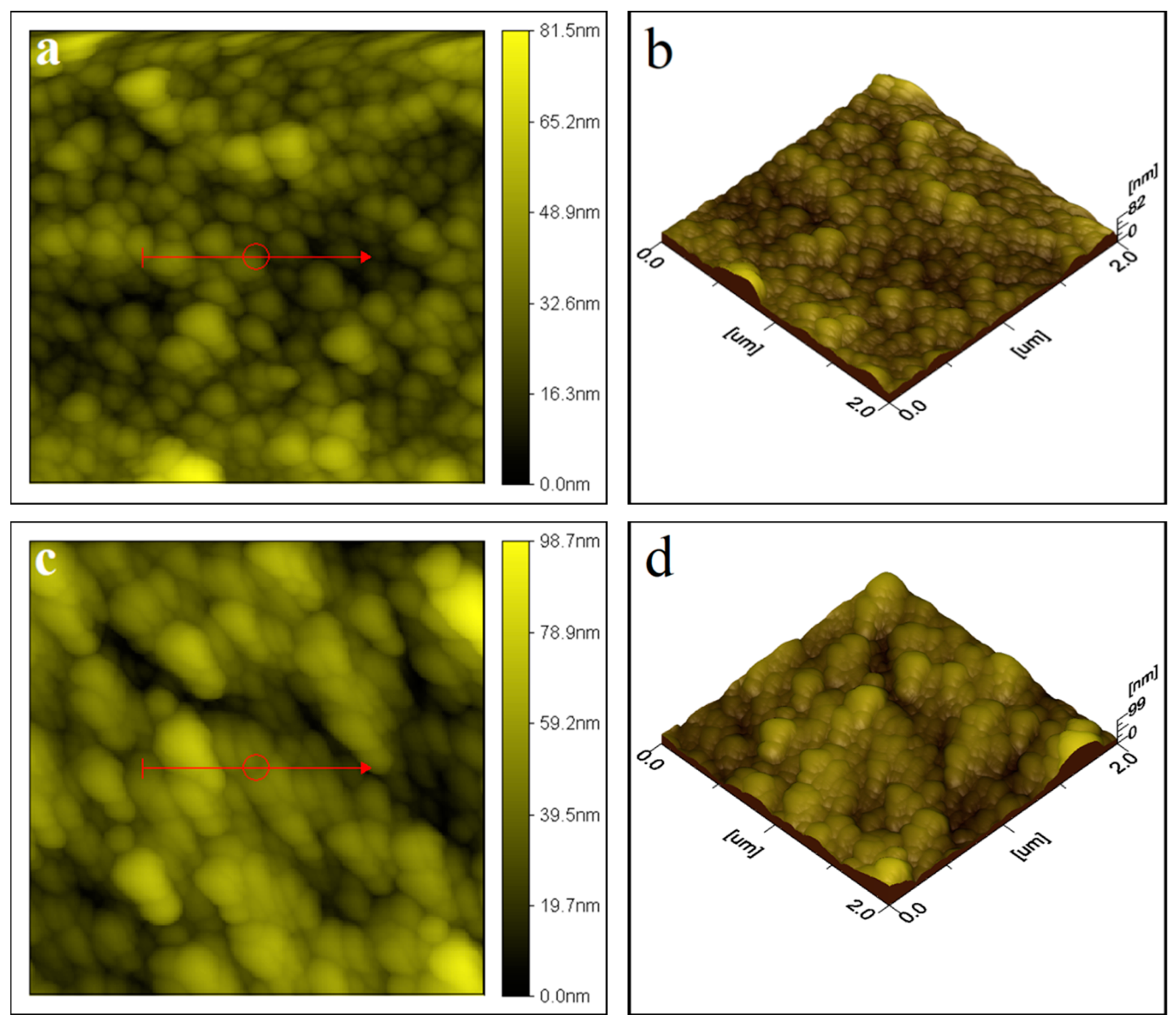
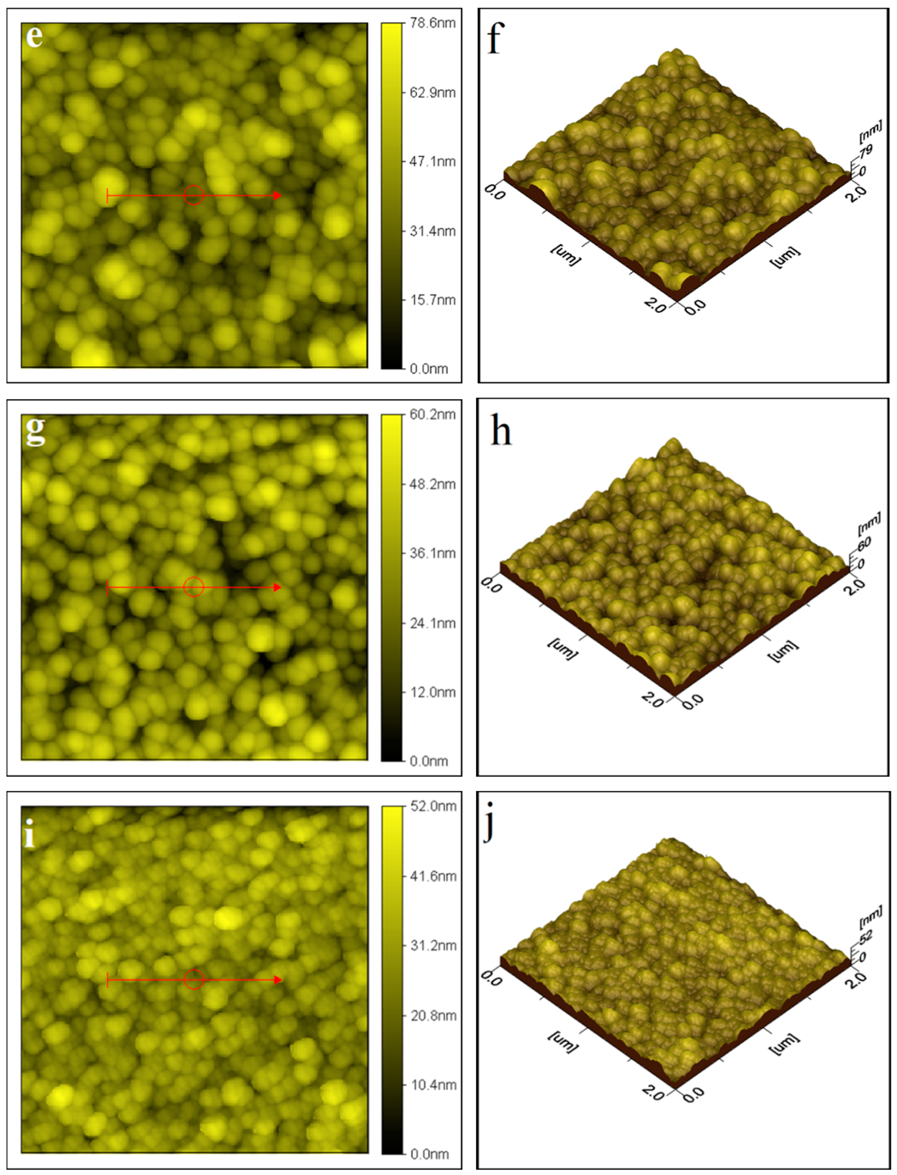
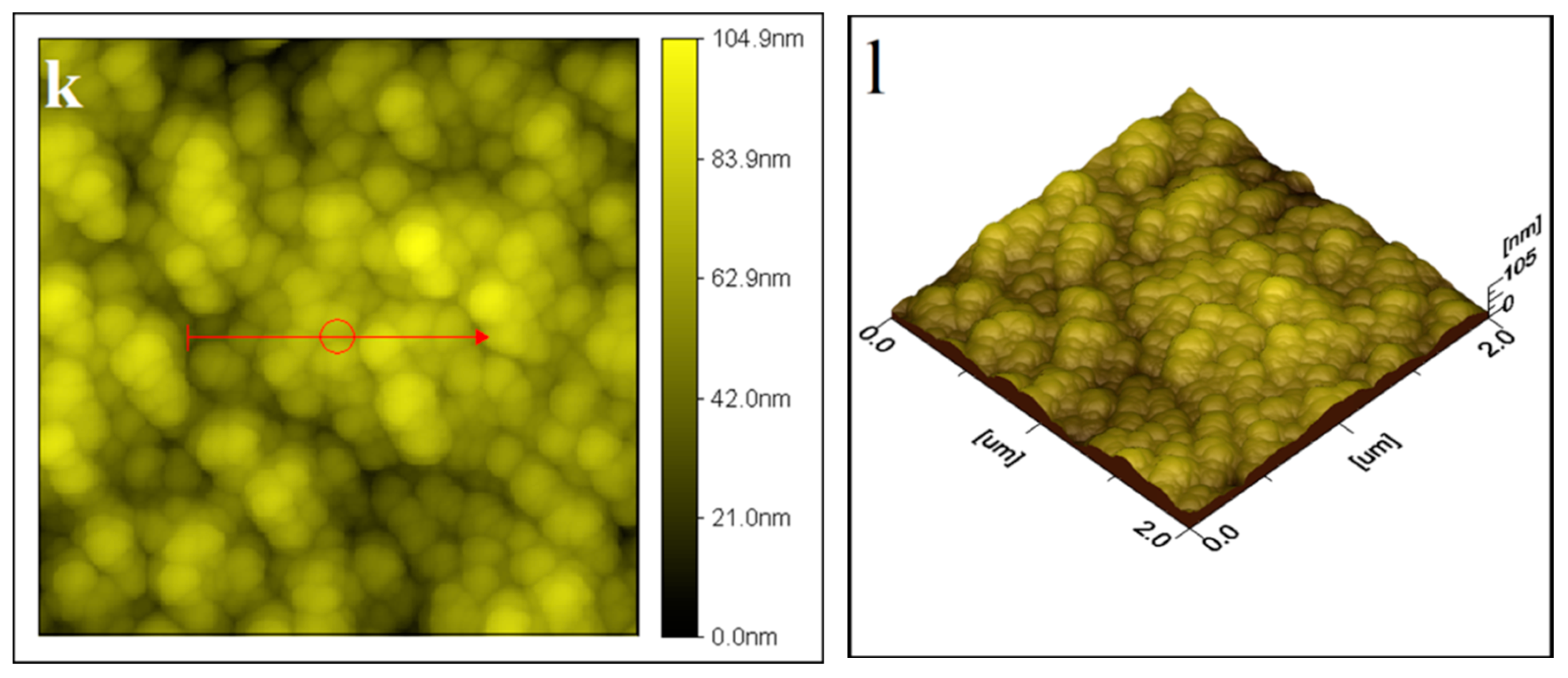
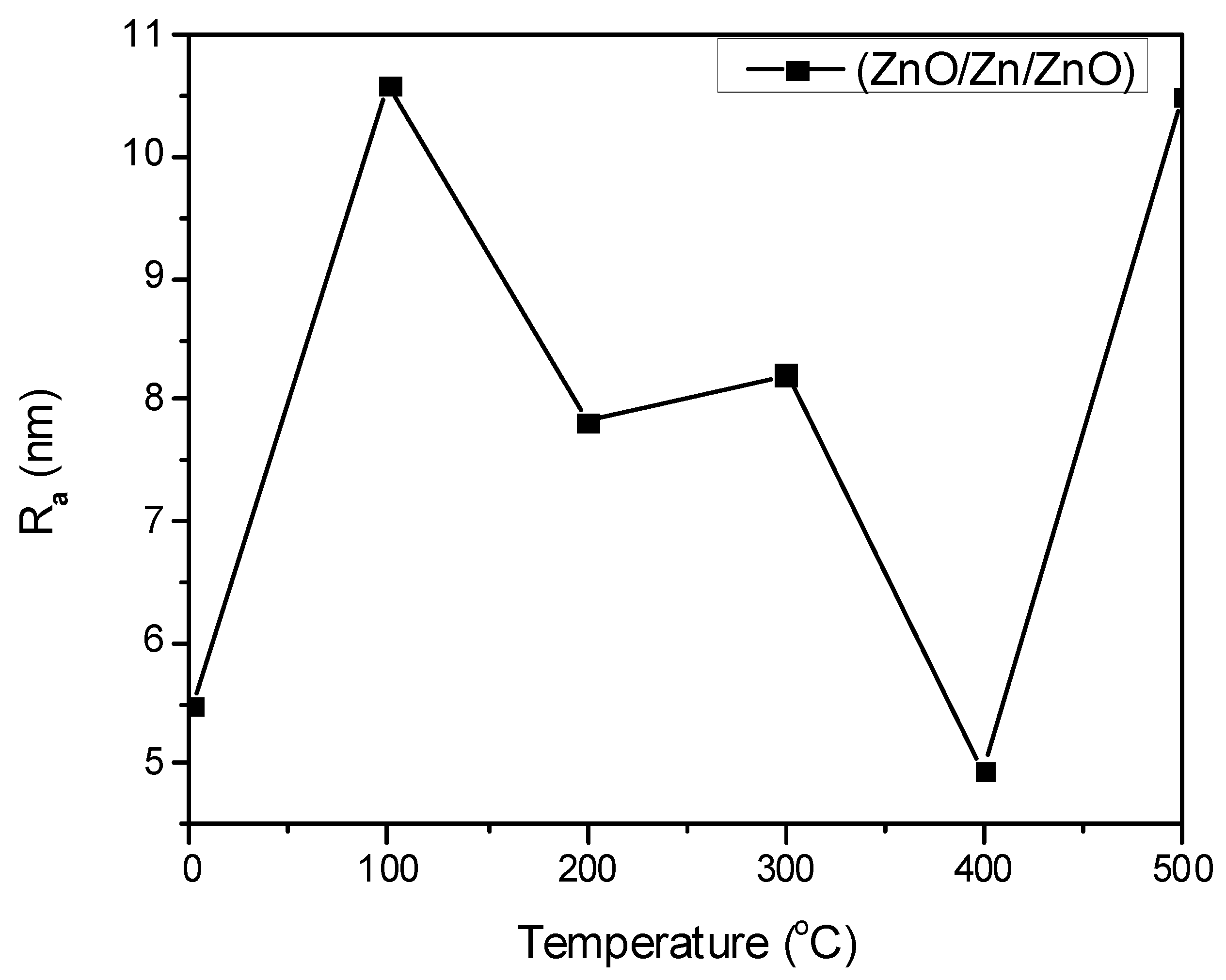
2.1.1. Atomic Force Microscopy (AFM) Analysis

Figure 1 shows atomic force microscopy (AFM) images of annealed thin films in comparison to as-deposited films, whereas Figure 2 describes the influence of annealing temperature on the average roughness (Ra) of the films. Ra measures the average length between the peaks and valleys and the deviation from the mean line on the entire surface within the sampling length. From Figure 1, one can observe that Ra first increases with an increase in the annealing temperature and then decreases to a minimum value. A minimum roughness was observed for the sample annealed at 400 °C, which is about 4.95 nm. A further increase in the annealing temperature results in an increase in the Ra value. A maximum Ra value was obtained for the sample annealed at 500 °C, which is about 10.60 nm. The initial decrease in roughness with increasing annealing temperature was attributed to the coalescence of the grains. A further increase in roughness with an increase in the annealing temperature may be due to the further increase in grain size. Moreover, the heterostructure is composed of three layers; that is, Zn is sandwiched between the ZnO layers. The melting point of Zn is 420 °C, whereas that of ZnO is 1975 °C. Increasing the annealing temperature from 400 °C to 500 °C changed the Zn phase from solid to liquid. The liquid Zn layer might penetrate or percolate into the interstitial pores in the underlying ZnO layers. This penetration can lead to a disruption in the uniformity of the ZnO structure, as the liquid Zn may fill voids and create localized regions of different densities or compositions. As can be seen, an increase in the peaks and valleys in the film results in an increase in the average roughness above the optimum value of the annealing temperature. The infiltration of liquid Zn into the ZnO layers can also promote the formation of microcracks or other structural imperfections as the film cools down and as Zn solidifies, leading to an increase in the Ra of the film. Furthermore, the increase in Ra at higher annealing temperatures can be linked to the thermodynamic instability introduced by the liquid phase of Zn. As Zn re-solidifies upon cooling, it may not return to its original crystalline orientation, leading to further imperfections and non-uniformities in the ZnO/Zn/ZnO heterostructure.

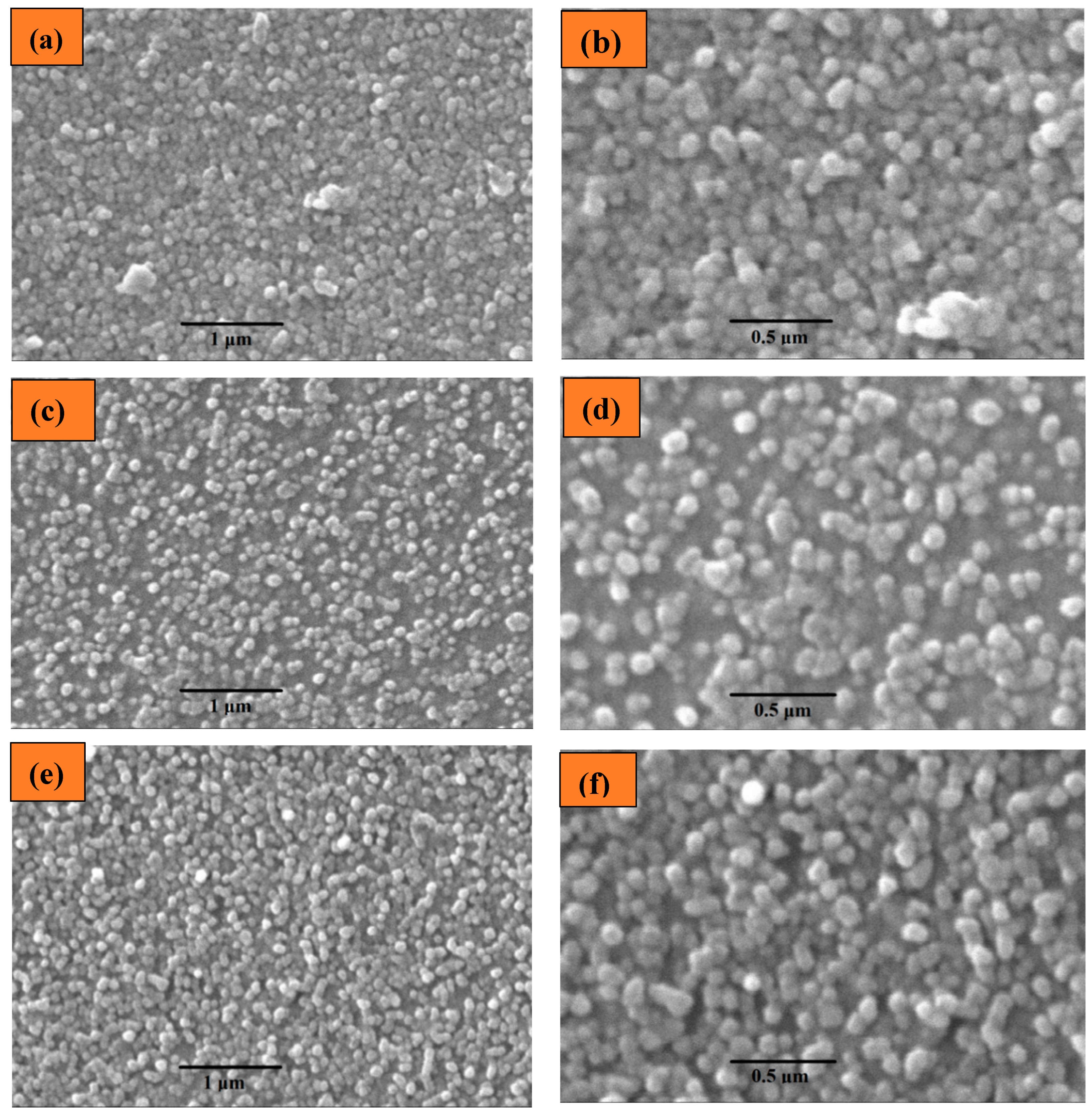
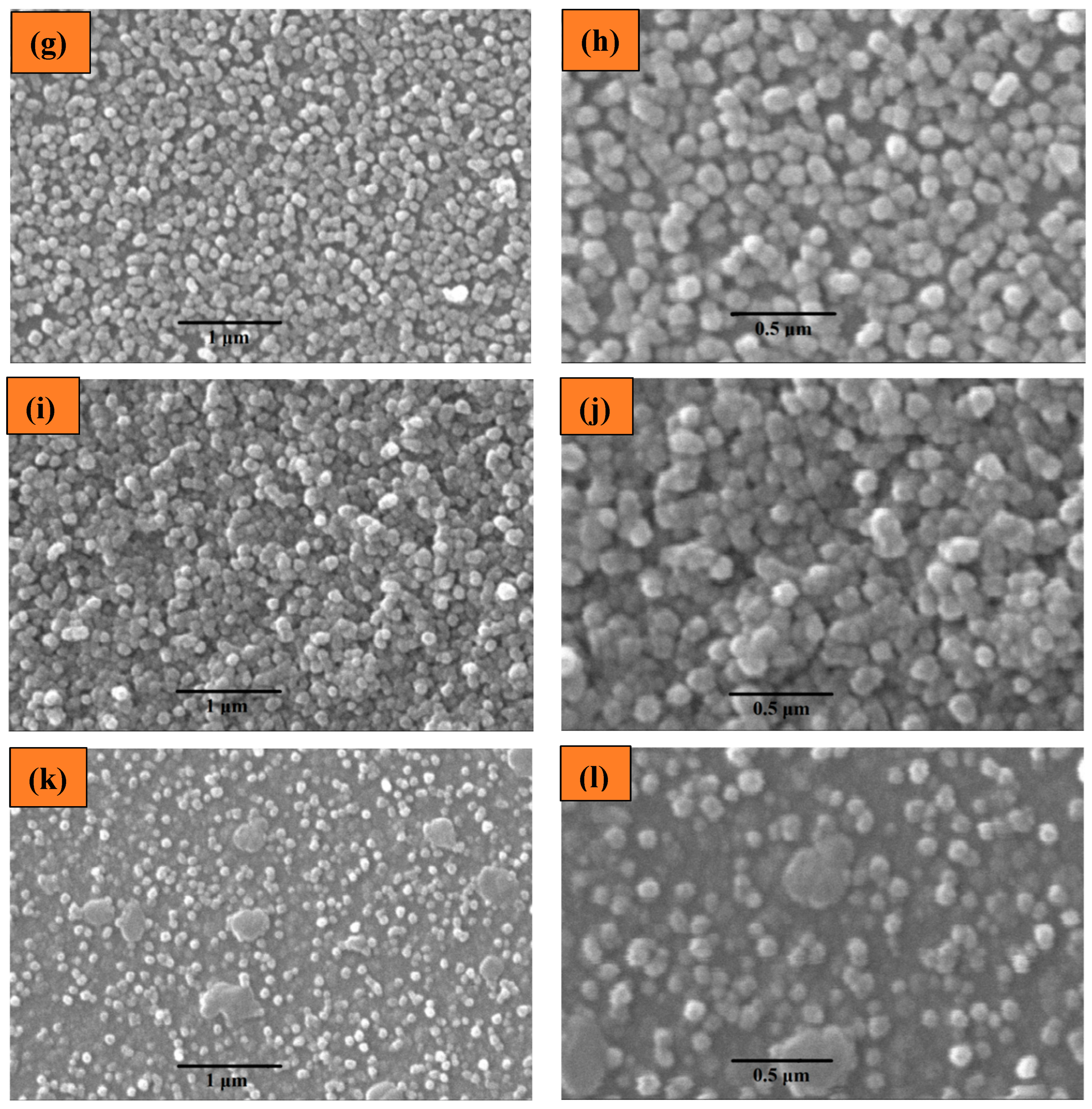
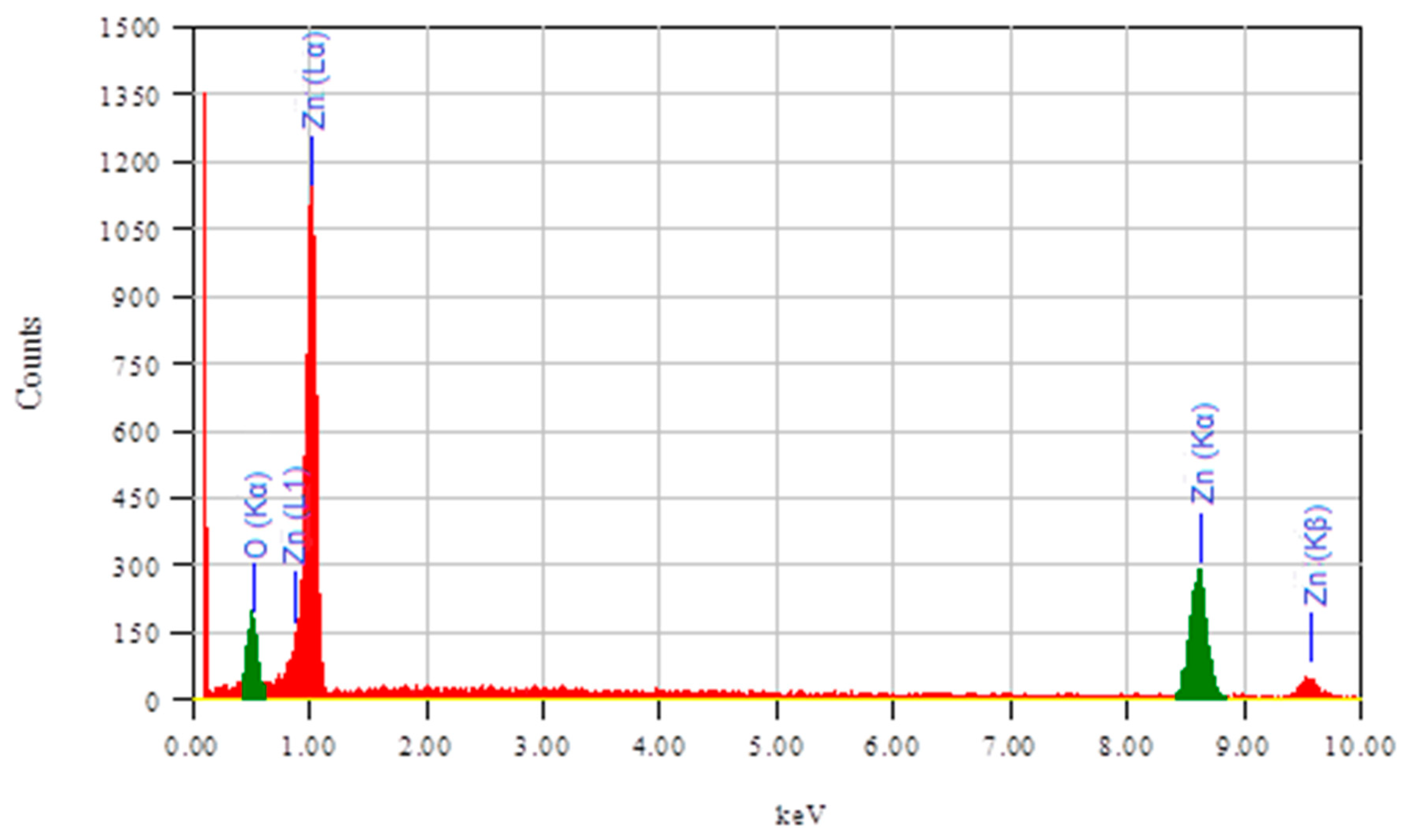
2.1.2. Scanning Electron Microscopy (SEM) Analysis

Figure 3 shows the scanning electron microscopy (SEM) images of the ZnO/Zn/ZnO heterostructure of the as-deposited thin film in comparison with annealed thin films. The annealed samples have a smooth surface morphology compared to the as-deposited thin films. However, the surface smoothness is disturbed by the higher annealing temperature. Moreover, the average particle size also has a great impact on the annealing temperature. Table 1 lists the average particle size calculated for all the thin films along with the annealing temperature.
From the table, we can see that the average particle size decreases with an increase in the post-heat treatment (annealing temperature). An optimum value of the particle size was calculated for the sample annealed at 400 °C. A further increase in temperature in the middle layer, which is comprised of Zn, affects the surface morphology and smoothness of the films. Figure 4 shows the energy dispersive X-ray (EDX) spectra of the film annealed at 400 °C, confirming that ZnO film is deposited.

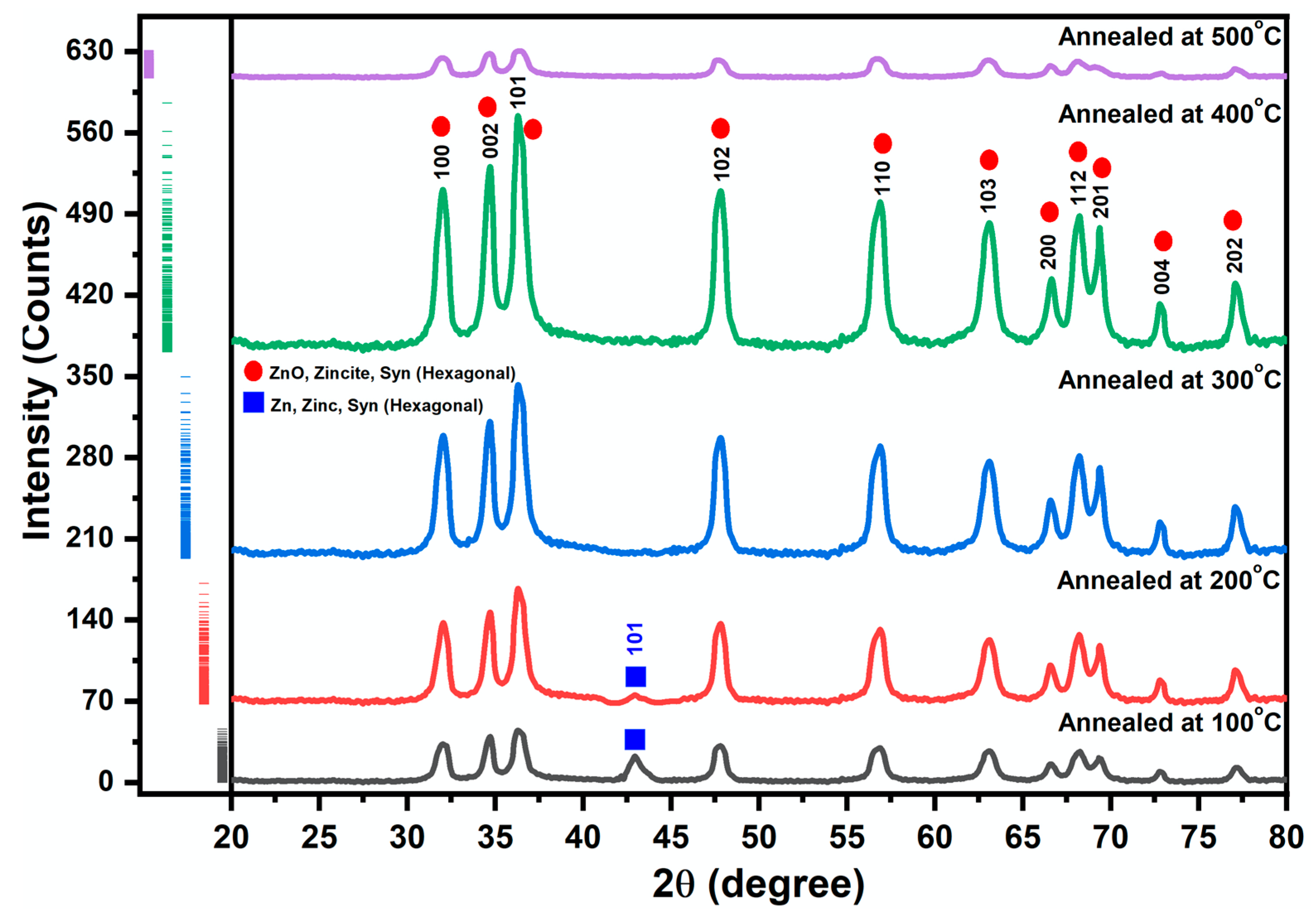
2.2. Structural Analysis

Figure 5 displays the XRD patterns of the as-prepared ZnO/Zn/ZnO thin films that were prepared and subjected to annealing temperatures of 100, 200, 300, 400, and 500 °C. XRD offers valuable information regarding the crystalline structure and phase composition of the samples at various annealing temperatures. The XRD patterns of the sample that underwent annealing at 100 °C indicated the existence of a zincite hexagonal crystal structure. The diffraction peaks observed in the figure match those of the hexagonal zincite ZnO. However, there was also an extra peak corresponding to metallic Zn. This suggests that a portion of the Zn still existed in its metallic form. The XRD spectrum of the sample annealed at 200 °C exhibited peaks corresponding to both Zn and ZnO. The identification of the ZnO peaks provides evidence for the creation of the hexagonal structure of zincite, whereas the Zn peak indicates that a portion of the zinc did no undergone conversion at this particular temperature. The samples annealed at 300 and 400 °C displayed XRD patterns indicative of pure ZnO with a hexagonal crystal structure. There were no discernible peaks in the spectra corresponding to metallic Zn. This indicates the complete transformation of Zn into ZnO, leading to the formation of a ZnO crystal structure with only one phase. Significantly, the strength of the diffraction peaks increased as the annealing temperature increased, culminating in the highest intensity at 400 °C. These findings indicate that the quality of the ZnO crystal structure is enhanced as the temperature increases, reaching its peak at 400 °C. However, the sample annealed at 500 °C exhibited a reduction in the intensity of the ZnO diffraction peaks in comparison to the sample annealed at 400 °C while still maintaining the pristine hexagonal structure of ZnO. The decrease in the maximum intensity at 500 °C can be ascribed to various factors. At elevated temperatures, excessive grain growth occurs, as discussed in the SEM and AFM results, and the particle size and roughness increase, resulting in the formation of imperfections within the crystal structure. The presence of these imperfections causes X-rays to disperse more widely, resulting in a decrease in the overall intensity of the diffraction patterns. Extended exposure to elevated temperatures can generate thermal stress in the thin film, which may lead to the formation of microcracks or other structural flaws that diminish the crystalline quality of the material.

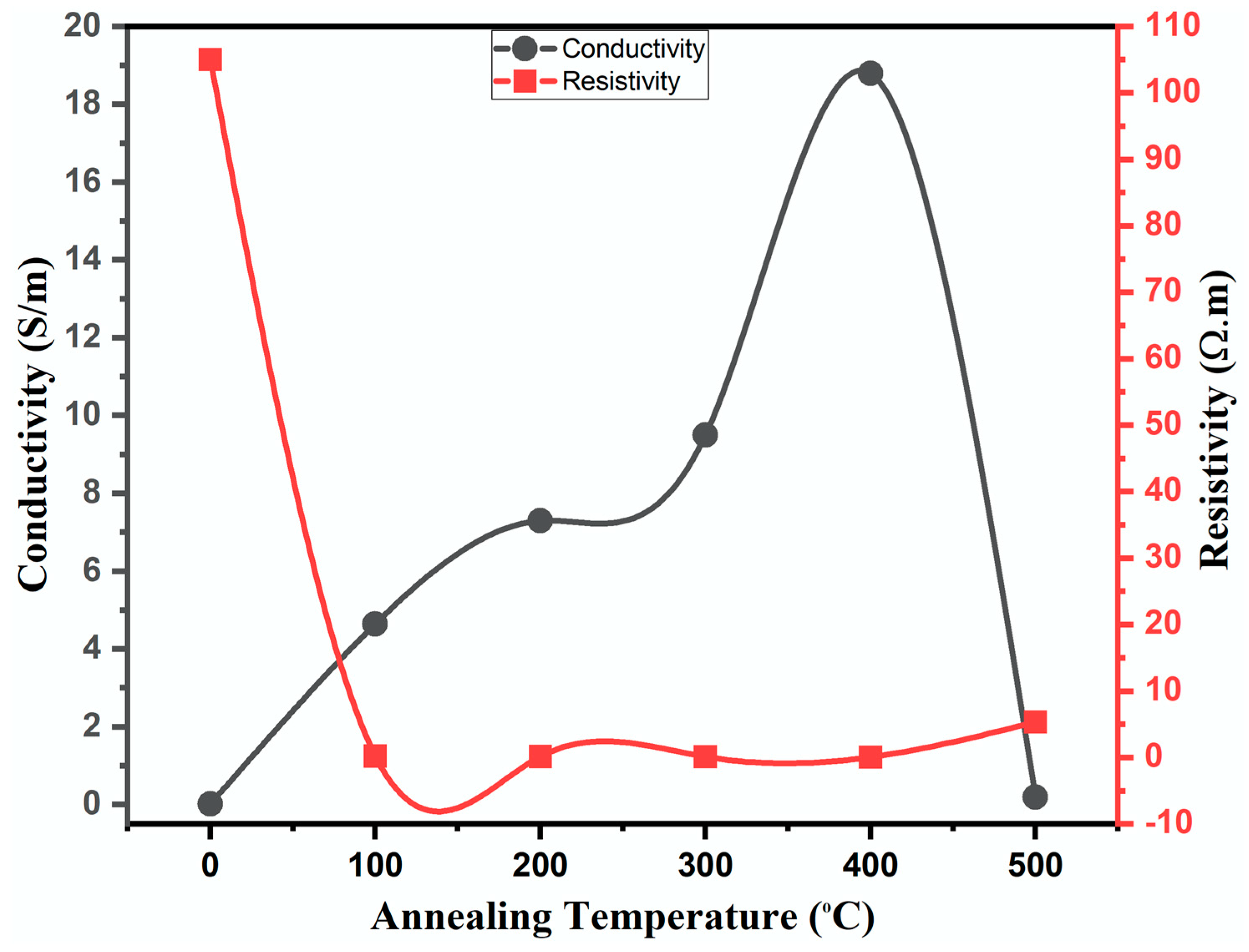
2.3. Electrical Properties

Figure 6 shows the electrical resistivity and conductivity of the thin films annealed at different temperatures. In addition, Table 2 lists the electrical resistivity and conductivity values of the annealed and deposited thin films. From the figure and table, we can see that the electrical resistivity/conductivity of the film changes with an increase in the annealing temperature. The electrical behaviour demonstrates a complex relationship among particle size, surface roughness, and electrical conductivity, which is closely connected to the microstructural evolution during thermal annealing. The electrical conductivity of the thin films exhibited a substantial increase from the as-deposited state to a thin film annealed at 400 °C, as displayed in Figure 6. This improvement in conductivity is linked to the reduction in particle size and enhancement in crystalline quality, as demonstrated by the XRD analysis, as well as a corresponding decrease in surface roughness, which facilitates crystalline quality. The decrease in surface roughness from the as-deposited thin film to the 400 °C annealed film indicates a smoother film surface, which minimizes scattering sites for charge carriers, thus enhancing conductivity. Smaller particle sizes and improved crystal structures decrease the number of grain boundaries, which are known to act as scattering centres for charge carriers (electrons and holes) [38,39,40]. The reduction in grain boundary scattering allows for more efficient carrier transport, thereby increasing the electrical conductivity of the films. However, a significant change occurred at 500 °C, where the particle size increased dramatically and the conductivity dropped sharply. This decline in conductivity can be ascribed to the formation of larger grains, which may introduce structural imperfections such as microcracks. These imperfections likely result from thermal stress or excessive grain growth, which disrupts the crystal structure and increases the scattering of carriers, ultimately leading to a higher electrical resistance [41]. This phenomenon aligns with the established understanding that while smaller grains typically increase resistance due to grain boundary scattering, excessively large grains can introduce new defects that also adversely affect conductivity.

3. Conclusions

In summary, magnetron sputtering was used to deposit hetero-structured (ZnO/Zn/ZnO) thin films on clean glass substrates. The resulting samples were annealed in an inert environment at 100, 200, 300, 400, and 500 °C. XRD analysis confirmed the presence and highly crystalline hexagonal structure of ZnO at 300 and 400 °C, whereas at other annealing temperatures, the sample either possessed metallic zinc or low crystallinity. Atomic force microscopy (AFM) and scanning electron microscopy (SEM) were used to effectively study the surface morphology and particle size. A Hall effect measurement device was used to analyse the electrical characteristics. The annealed thin-film data were plotted in comparison with the deposited thin film. AFM analysis indicated that the average roughness (Ra) of the film decreased with an increase in the annealing temperature, reaching an optimum value of 4.95 nm for the sample annealed at 400 °C, and then increased with a further increase in the annealing temperature. SEM analysis showed that the particle sizes initially decreased with increasing annealing temperature but increased at higher temperatures. The Hall effect measurement system showed that the electrical resistivity decreased for the annealed samples. In addition, the resistivity showed a good relationship with the surface roughness of the thin films; the lower the surface roughness with lower scattering centres of charge carriers, the lower the resistivity. The sample annealed at 400 °C exhibited the lowest resistivity.

4. Experimental

This section discusses the fabrication process of a hetero-structured (ZnO/Zn/ZnO) thin film and its thermal annealing at different temperatures and gives the description used to analyse the morphological, topographical, structural, and electrical properties of the samples. Magnetron sputtering was used to deposit a hetero-structured (ZnO/Zn/ZnO) thin film on a glass substrate, which was subsequently annealed at 100, 200, 300, 400, and 500 °C.

4.1. Films Deposition

4.1.1. Substrate Preparation

The cleanliness of the substrate is crucial for achieving high-quality thin films. Soda-lime glass slides (SLG) (cat. No. 7105) were cut into small squares (10 cm × 10 cm × 1 cm) using a diamond saw cutter. The cleaning process involved several steps. First, the substrates were immersed in methanol and cleaned ultrasonically for 30 min to remove organic residues. Washing with the soap solution was then carried out, followed by rinsing in deionised water. Subsequently, the substrates were immersed in a chromic acid solution for 20 min. Finally, the substrates were ultrasonically cleaned with water for 30 min. Subsequently, the substrate surface was dried by blowing pressurised inert gas and immediately transferred to the deposition chamber.

4.1.2. Sputtering System and Film Deposition Process

Deposition of ZnO and Zn thin films over SLG substrates was performed using a disk-shaped ZnO and Zn target (100 mm diameter, 8.25 mm thickness) in a magnetron sputtering system (Alliance Concept, DP650, Annecy, France). The system consisted of mechanical and turbomolecular pumps, sputtering guns, RF and DC power supplies, and heating and bias capabilities for substrate support. Each film deposition cycle included the following steps: After loading the substrates, the chamber was evacuated to a base pressure of a few microtorr, followed by the introduction of argon gas. The argon flow rate was maintained at 20 sccm to achieve a pressure of 10 mTorr. The DC power was then turned on, and its value was adjusted to the desired level. Initially, the target was sputtered with its shutter closed for approximately 15 min to remove any native oxide layer present on its surface. Subsequently, ZnO (bottom layer), Zn (middle layer), and ZnO (top layer) film deposition was performed to fabricate films with a thickness of 1.5 μm, 30 nm, and 75 nm, respectively. The base pressure was maintained at 7.49 × 10⁻⁶ bar, and a 300 W DC power source was employed to keep the potential difference between the target and glass substrate constant. During growth, the film thickness was monitored using a quartz crystal microbalance. The sputtered samples were annealed in an inert argon atmosphere for 1 h at 100, 200, 300, 400, and 500 °C. The deposition parameters are listed in Table 3.

4.2. Characterization Tools

The surface morphologies of the as-grown and annealed multilayer structures were examined using scanning electron microscopy (SEM) (JSM-840, JEOL, Tokyo, Japan) with an operating voltage of 15–20 kV, spot size of 30–50 nm, and working distance of 10 mm. For SEM analysis, samples were coated by sputtering 100 nm gold, and small silver strips were placed on the sample to make it conductive. Atomic force microscopy (AFM) (JEOL SPM-5200) was used to examine the topography and measure the surface roughness of the multilayer structure while operating in the non-contact mode with scan sizes of (10 × 10) and (3 × 3) μm2. X-ray diffraction (XRD) was used to determine the structural and phase purity of the prepared samples using a D8 ADVANCE, Bruker, Germany instrument over the range of 20–80° with Cu Kα radiation (λ = 1.5418Å) and a step size and dwell time of 0.041 and 3 s, respectively. The electrical conductivity was measured using either a four-point electrical resistance probe or a Hall automated measuring system utilizing the Van-Der-Pauw method (Ecopia HMS-5000, Bridge Technology, USA). Four electrodes of gold paste were placed at four different equal points, and four needle tips were placed to measure the voltage and current.

Funding

This work was supported by the Deanship of Scientific Research, Vice Presidency for Graduate Studies and Scientific Research, King Faisal University, Saudi Arabia (Grant No. 3,061).

Data Availability Statement

The original contributions presented in the study are included in the article, further inquiries can be directed to the author.

Conflicts of Interest

The author declares that he has no known competing financial interests or personal relationships that could have appeared to influence the work reported in this paper.

References

  1. Khan, M.; Islam, M. Deposition and Characterization of Molybdenum Thin Films Using DC Plasma Magnetron Sputtering 1. Semiconductors 2013, 47, 1610–1615. [Google Scholar] [CrossRef]
  2. Hussein, A.K. Applications of nanotechnology in renewable energies—A comprehensive overview and understanding. Renew. Sustain. Energy Rev. 2015, 42, 460–476. [Google Scholar] [CrossRef]
  3. Ali, S.; Saleem, S.; Salman, M.; Khan, M. Synthesis, structural and optical properties of ZnS–ZnO nanocomposites. Mater. Chem. Phys. 2020, 248, 122900. [Google Scholar] [CrossRef]
  4. Sharma, D.K.; Shukla, S.; Sharma, K.K.; Kumar, V. A review on ZnO: Fundamental properties and applications. Mater. Today Proc. 2020, 49, 3028–3035. [Google Scholar] [CrossRef]
  5. Kumar, V.P.S.; Manikandan, N.; Nagaprasad, N.; Letatesfaye, J.; Krishnaraj, R. Analysis of the Performance Characteristics of ZnO Nanoparticles’ Dispersed Polyester Oil. Adv. Mater. Sci. Eng. 2022, 2022, 4844979. [Google Scholar] [CrossRef]
  6. Liu, C.; Burghaus, U.; Besenbacher, F.; Wang, Z.L. Preparation and Characterization of Nanomaterials for Sustainable Energy Production. ACS Nano 2010, 4, 5517–5526. [Google Scholar] [CrossRef]
  7. Sanchez, C.; Lebeau, B.; Chaput, F.; Boilot, J. Optical Properties of Functional Hybrid Organic-Inorganic Nanocomposites. Adv. Mater. 2004, 15, 1969–1994. [Google Scholar] [CrossRef]
  8. Du, Y.; Zhao, F.; Liu, L.; Gao, Y.; Xing, L.; Li, Q.; Fu, C.; Zhong, Z.; Zhang, X. Improvement of bond strength between ZnO nanorods and carbon fibers using magnetron sputtered ZnO films as the interphase. CrystEngComm 2017, 19, 868–875. [Google Scholar] [CrossRef]
  9. Ferhati, H.; Djeffal, F.; Kacha, K. Optimizing the optical performance of ZnO/Si-based solar cell using metallic nanoparticles and interface texturization. Optik 2018, 153, 43–49. [Google Scholar] [CrossRef]
  10. Klingshirn, C.; Priller, H.; Decker, M.; Bruckner, J.; Kalt, H.; Hauschild, R.; Zeller, J.; Waag, A.; Bakin, A.; Wehmann, H.; et al. Excitonic properties of ZnO. Adv. Solid State Phys. 2005, 45, 275–287. [Google Scholar]
  11. Kou, L.Z.; Guo, W.L.; Li, C. Piezoelectricity of ZNO and its nanostructures. In 2008 Symposium on Piezoelectricity, Acoustic Waves, and Device Applications; IEEE: New York, NY, USA, 2008; pp. 354–359. [Google Scholar] [CrossRef]
  12. Chen, Z.; Wang, J.; Wu, H.; Yang, J.; Wang, Y.; Zhang, J.; Bao, Q.; Wang, M.; Ma, Z.; Tress, W.; et al. A Transparent Electrode Based on Solution-Processed ZnO for Organic Optoelectronic Devices. Nat. Commun. 2022, 13, 4387. [Google Scholar] [CrossRef]
  13. Blom, F.R.; Bauhuis, G. 365 RF Planar Magnetron Sputtered ZnO Films II: Electrical Properties. Thin Solid Film. 1991, 204, 365–376. [Google Scholar] [CrossRef]
  14. Mahmood, F.S.; Gould, R.D.; Hassan, A.K.; Salih, H.M. DC properties of ZnO thin films prepared by rf magnetron sputtering. Thin Solid Film. 1995, 770, 95–98. [Google Scholar]
  15. Ponja, S.D.; Sathasivam, S.; Parkin, I.P.; Carmalt, C.J. Highly conductive and transparent gallium doped zinc oxide thin films via chemical vapor deposition. Sci. Rep. 2020, 10, 1–7. [Google Scholar]
  16. Sharma, R.; Yoo, S. ZnO in organic electronics. In Nanostructured Zinc Oxide: Synthesis, Properties and Applications; Elsevier: Amsterdam, The Netherlands, 2021. [Google Scholar] [CrossRef]
  17. Saitou, M.; Makabe, A.; Tomoyose, T. AFM study of surface roughening in sputter-deposited nickel films on ITO glasses. Europhys. Lett. 2000, 52, 185–188. [Google Scholar] [CrossRef]
  18. Hasan, S.A.; Gibson, D.; Song, S.; Wu, Q.; Ng, W.P.; McHale, G.; Dean, J.; Fu, Y.Q. ZnO thin film based flexible temperature sensor. Proc. IEEE Sens. 2017, 2017, 1–3. [Google Scholar]
  19. Xuan, J.; Zhao, G.; Sun, M.; Jia, F.; Wang, X.; Zhou, T.; Yin, G.; Liu, B. Low-temperature operating ZnO-based NO2 sensors: A review. RSC Adv. 2020, 10, 39786–39807. [Google Scholar] [CrossRef]
  20. Nomura, K.; Ohta, H.; Ueda, K.; Kamiya, T.; Hirano, M.; Hosono, H. Thin-Film Transistor Fabricated in Single-Crystalline Transparent Oxide Semiconductor. Nanotechnology 2003, 300, 1269–1272. [Google Scholar] [CrossRef]
  21. Bel Hadj Tahar, R.; Ban, T.; Ohya, Y.; Takahashi, Y. Tin doped indium oxide thin films: Electrical properties. J. Appl. Phys. 1998, 83, 2631–2645. [Google Scholar] [CrossRef]
  22. Kind, B.H.; Yan, H.; Messer, B.; Law, M.; Yang, P. Nanowire Ultraviolet Photodetectors and Optical. Adv. Mater. 2002, 14, 200–202. [Google Scholar] [CrossRef]
  23. Zaier, A. Annealing effects on the structural, electrical and optical properties of ZnO thin films prepared by thermal evaporation technique. J. King Saud Univ. Sci. 2015, 27, 356–360. [Google Scholar] [CrossRef]
  24. Husna, J.; Aliyu, M.M.; Islam, M.A.; Chelvanathan, P. Influence of Annealing Temperature on the Properties of ZnO Thin Films Grown by Sputtering. Energy Procedia 2012, 25, 55–61. [Google Scholar] [CrossRef]
  25. Shivaraj, B.W.; Murthy, H.N.N.; Krishna, M.; Satyanarayana, B.S. Effect of Annealing Temperature on Structural and Optical properties of Dip and Spin coated ZnO Thin Films. Procedia Mater. Sci. 2015, 10, 292–300. [Google Scholar] [CrossRef]
  26. Films, T.S.; Engineering, E.; Enschede, A.E. 1.1. Sputtered thin film ZnO. Thin Solid Film. 1991, 204, 349–364. [Google Scholar]
  27. Soci, C.; Zhang, A.; Xiang, B.; Dayeh, S.A.; Aplin, D.P.R.; Park, J.; Bao, X.Y.; Lo, Y.H.; Wang, D. ZnO Nanowire UV Photodetectors with High Internal Gain. Nano Lett. 2007, 7, 1003–1009. [Google Scholar] [CrossRef]
  28. Gurylev, V.; Perng, T.P. Defect engineering of ZnO: Review on oxygen and zinc vacancies. J. Eur. Ceram. Soc. 2021, 41, 4977–4996. [Google Scholar] [CrossRef]
  29. Heremans, J.P. The ugly duckling. Nature 2014, 508, 327–328. [Google Scholar] [CrossRef]
  30. McCluskey, M.D. Defects in ZnO. In Defects in Advanced Electronic Materials and Novel Low Dimensional Structures; Elsevier: Amsterdam, The Netherlands, 2018. [Google Scholar]
  31. Gorla, C.R.; Emanetoglu, N.W.; Liang, S.; Mayo, W.E.; Lu, Y.; Wraback, M.; Shen, H.; Gorla, C.R.; Emanetoglu, N.W.; Liang, S.; et al. Structural, optical, and surface acoustic wave properties of epitaxial ZnO films grown on (0112) sapphire by metalorganic chemical vapor deposition. J. Appl. Phys. 2009, 85, 2595–2602. [Google Scholar] [CrossRef]
  32. Huang, P.; Huang, C.; Lin, M.; Chou, C.; Hsu, C.; Kuo, C. The Effect of Sputtering Parameters on the Film Properties of Molybdenum Back Contact for CIGS Solar Cells. Int. J. Photoenergy 2013, 2013, 390824. [Google Scholar] [CrossRef]
  33. Kumar, S.; Gupta, V.; Sreenivas, K. Synthesis of photoconducting ZnO nano-needles using an unbalanced magnetron sputtered ZnO/Zn/ZnO multilayer structure. Nanotechnology 2005, 16, 1167. [Google Scholar] [CrossRef]
  34. McCluskey, M.D.; Jokela, S.J. Defects in ZnO. J. Appl. Phys. 2009, 106, 071101. [Google Scholar] [CrossRef]
  35. Mohamed, D. Influence of Low Ag Doping on Structural, Morphological and Optical Properties of Sol-Gel Dip-Coated Nanostructured ZnO Thin Films. Int. J. Nat. Sci. 2016, 4, 15–28. [Google Scholar]
  36. Chen, W.-T.; Fang, P.-C.; Chen, Y.-W.; Chiu, S.-J.; Ku, C.-S.; Brahma, S.; Lo, K.-Y. Zn dots coherently grown as the seed and buffer layers on Si(111) for ZnO thin film: Mechanism, in situ analysis, and simulation. J. Vac. Sci. Technol. A 2022, 40, 063403. [Google Scholar] [CrossRef]
  37. Fu, Z.; Lin, B.; Liao, G.; Wu, Z. The effect of Zn buffer layer on growth and luminescence of ZnO films deposited on Si substrates. J. Cryst. Growth 1998, 193, 316–321. [Google Scholar] [CrossRef]
  38. Seto, J.Y.W. The electrical properties of polycrystalline silicon films. J. Appl. Phys. 1975, 46, 5247–5254. [Google Scholar] [CrossRef]
  39. Bhuvana, K.P.; Elanchezhiyan, J.; Gopalakrishnan, N.; Balasubramanian, T. Influence of grain size on the properties of AlN doped ZnO thin film. Mater. Sci. Semicond. Processing. 2011, 14, 84–88. [Google Scholar] [CrossRef]
  40. Zhu, M.W.; Wang, Z.J.; Chen, Y.N.; Wang, H.L.; Zhang, Z.D. Effect of grain boundary on electrical properties of polycrystalline lanthanum nickel oxide thin films. Appl. Phys. A 2013, 112, 1011–1018. [Google Scholar] [CrossRef]
  41. Imajo, T.; Suemasu, T.; Toko, K. Strain effects on polycrystalline germanium thin films. Sci. Rep. 2021, 11, 8333. [Google Scholar] [CrossRef]
Figure 1. AFM 2D and 3D images of thin films: (a,b) as deposited, (c,d) annealed at 100 °C, (e,f) annealed at 200 °C, (g,h) annealed at 300 °C, (i,j) annealed at 400 °C, and (k,l) annealed at 500 °C.
Inorganics 12 00236 g001aInorganics 12 00236 g001bInorganics 12 00236 g001c
Figure 2. Average roughness (Ra) vs. annealing temperature of thin films.
Inorganics 12 00236 g002
Figure 3. SEM images of thin films with low and high magnifications: (a,b) as deposited, (c,d) annealed at 100 °C, (e,f) annealed at 200 °C, (g,h) annealed at 300 °C, (i,j) annealed at 400 °C, and (k,l) annealed at 500 °C.
Inorganics 12 00236 g003aInorganics 12 00236 g003b
Figure 4. EDX spectra of hetero-structured ZnO/Zn/ZnO thin film annealed at 400 °C.
Inorganics 12 00236 g004
Figure 5. XRD spectra of ZnO/Zn/ZnO thin film annealed at 100, 200, 300, 400, and 500 °C.
Inorganics 12 00236 g005
Figure 6. Resistivity/conductivity vs. annealing temperature of thin films.
Inorganics 12 00236 g006
Table 1. Average particle size of thin films annealed at different temperatures in comparison to the as-deposited sample.
S. No.Thin FilmAverage Particle Size
1As deposited74.41 ± 1.75 nm
2100 °C78.08 ± 1.83 nm
3200 °C66.85 ± 1.62 nm
4300 °C54.46 ± 1.23 nm
5400 °C50.67 ± 1.02 nm
6500 °C163.00 ± 2.51 nm
Table 2. Electrical resistivity and conductivity values of thin films annealed at different temperatures in comparison to a deposited thin film.
S. No.Thin FilmElectrical Conductivity (S/m)Electrical Resistivity (Ω.m)
1As deposited0.0095105
2100 °C4.6370.2157
3200 °C7.2920.1371
4300 °C9.490.105
5400 °C18.790.05321
6500 °C0.1875.348
Table 3. Deposition parameters of ZnO/Zn/ZnO thin films heterostructure.
Deposition ParametersZnOZnZnO
Pressure (mTorr)255050
Power (Watt)300300300
Thickness1.5 µm30 nm75 nm
Annealing Temperature (°C)
100200300400500
Disclaimer/Publisher’s Note: The statements, opinions and data contained in all publications are solely those of the individual author(s) and contributor(s) and not of MDPI and/or the editor(s). MDPI and/or the editor(s) disclaim responsibility for any injury to people or property resulting from any ideas, methods, instructions or products referred to in the content.

