Article

Design of a Novel Magnetic Induction Switch with a Permalloy Film and a Trans-Impedance Amplifier Circuit

1
Department of Electrical Engineering, School of Internet of Things Engineering, Jiangnan University, Wuxi 214122, China
2
Institute of Advanced Technology, Jiangnan University, Wuxi 214122, China
*
Author to whom correspondence should be addressed.
Inventions 2024, 9(1), 4; https://doi.org/10.3390/inventions9010004
Submission received: 2 December 2023 / Revised: 21 December 2023 / Accepted: 22 December 2023 / Published: 27 December 2023
(This article belongs to the Special Issue From Sensing Technology towards Digital Twin in Applications)

Abstract

:
At present, magnetic induction switches are widely used in industrial automation control and biological sensing systems. A core module composed of a magnetic sensing device and a signal conditioning circuit is designed and analyzed in this paper. Utilizing a permalloy film with the anisotropic magneto-resistance (AMR) effect, the novel magnetic induction switch shows its ability to correctly detect the direction of magnetic fields. Furthermore, an interfacial circuit based on a trans-impedance amplifier (TIA) is designed to measure and regulate the output signal of the sensing device. Accurate simulation results show the gain of the TIA reaches up to 51.36 dB with a bandwidth of 1.3 GHz and a power consumption of 3.65 mW. The outstanding performance of the proposed module demonstrates the possibility of solving the problems induced by high input impedance, high frequency, and parasitic effects in magnetic induction switches.

1. Introduction

As a type of non-contact switch, the magnetic induction switch is widely used in many areas, such as industrial automation control, biological sensing, and microparticle detection [1,2,3,4]. Its outstanding properties, including its high switching speed, high sensitivity, and large switching capacity, help it adapt to different working environments. However, in practical applications, the maximum operating frequency of the switch is usually limited. Meanwhile, the current induced in the sensing device is relatively low, so a high-precision processing circuit is needed [5,6].
A magnetic sensing device is usually made of a magnetically sensitive material, with the following processing circuit used to construct the core module of the switch. Fina et al. [7] studied the properties of the materials of a sensing device. They reported the polarization of the magnetic switch in epitaxial orthorhombic YMnO3 thin films. It was found that the reported field-induced switching is consistent with the existence of a cycloidal magnetic order in YMnO3. An approach to realizing field-free deterministic perpendicular magnetic switching with a ferromagnetic metal/non-magnetic metal/ferromagnetic metal (FM/NM/FM) structure is presented by Chen et al. [8], in which the large spin Hall angle of the transition metal β-W is used. In addition, in terms of processing circuits, an innovative direct current (DC) circuit breaker based on a magnetic induction current commutation module is proposed by Wu et al. [9].
In this paper, a novel module based on a sensing device made of a permalloy (PM) film and a current processing circuit is proposed. It can be used to determine the direction of a magnetic field along the Z-axis, which is perpendicular to the design plane of the PM film. Through the subsequent processing circuit, it outputs a high or low level, acting as a switch.
This paper is organized as follows. A sensor based on the anisotropic magneto-resistance (AMR) effect is first designed and fabricated, and one PM strip is inserted into the sensor, acting as the sensing device. From the perspective of simplicity and versatility, the strip is applied with a fixed voltage, and the principle of the sensing device is analyzed briefly. Next, a differential circuit for a current comparison is presented. The current of the sensing device is used as the input of the circuit, and an output signal at a high or low level is obtained by comparing it with the reference current. Finally, in the case of either a low or high frequency, a trans-impedance amplifier (TIA) circuit is proposed to solve the problems of increased input impedance and a large parasitic effect.

2. Materials and Methods
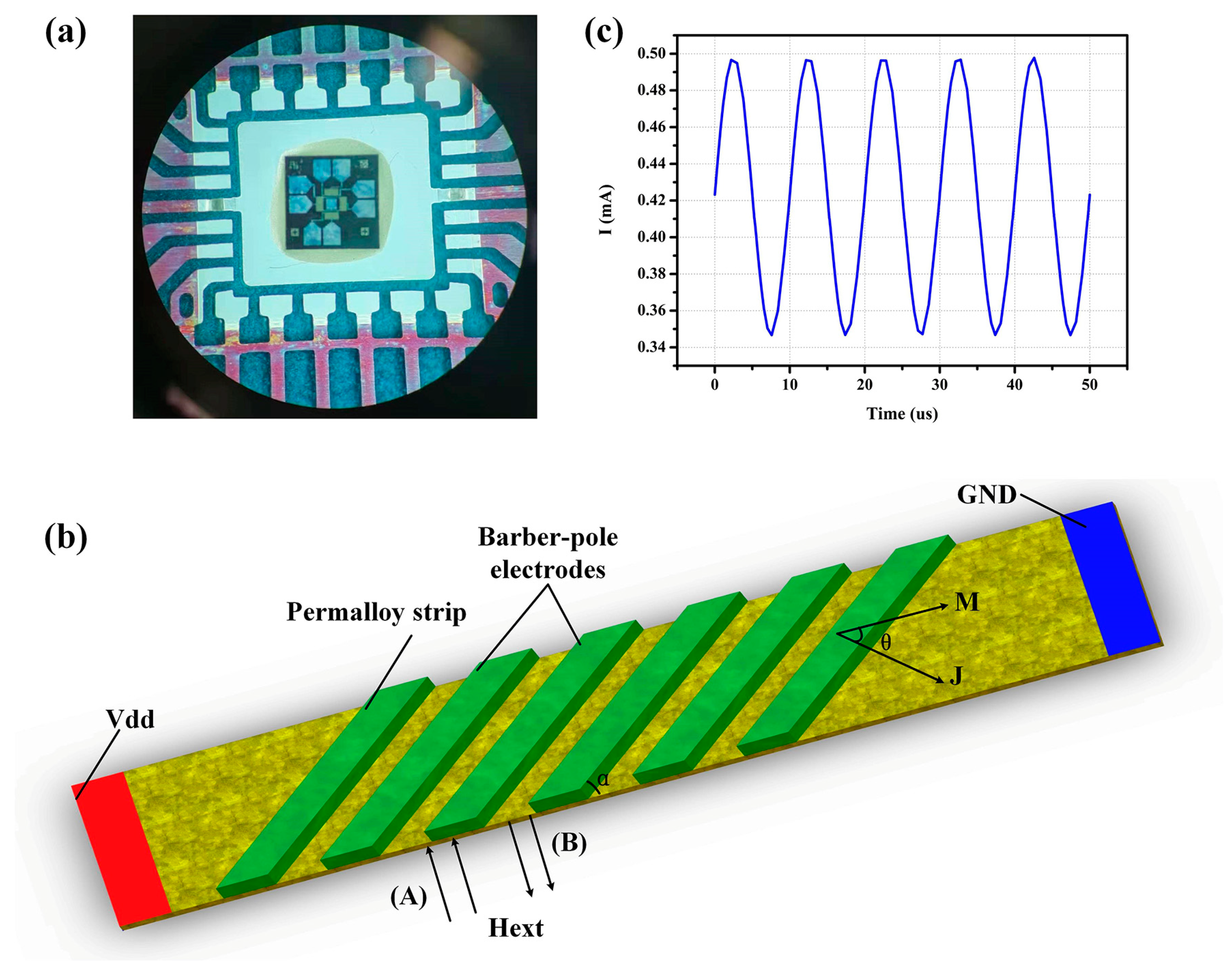
2.1. Sensing Device

Among the magnetic sensing devices developed, magnetic sensors based on the AMR effect are widely used due to their high sensitivity, large temperature range, low power consumption, and low cost [10,11,12]. The AMR effect is caused by the anisotropic scattering of 4s electrons in the exchanged split 3D orbitals [13]. This effect is obvious in PM films [14,15]. Therefore, a PM film made of 80% nickel and 20% iron is deposited on the device via magnetron sputtering. Its surface roughness, measured using an atomic force microscope (AFM), is shown in Figure 1a. The average roughness is 1.985 nm, qualifying it for further fabrication as a planar magnetic device [8]. The film is then patterned into a strip structure. Due to the shape anisotropy of the strip pattern, it can be easily magnetized along the long axis. In addition, a barber-pole electrode [16] is introduced on the PM film as it can rotate the direction of the current by an angle of 45° or 135° in the absence of a magnetic field ( H e x t ). Thus, the output voltage shows a linear relationship around zero magnetic field. Additionally, in actual working conditions, the sensor can be affected by temperature changes. The output signal of the PM film can be changed by its environment, which degrades the stability and accuracy of the sensor. For this reason, the Wheatstone bridge (WB) structure is adopted [2,17]. The WB structure contains four branches, and each branch consists of one or more PM strips. When the external magnetic field intensity H e x t changes, the WB outputs the measured results of the sensor in the form of a differential voltage. Through the differential outputs of the bridge, the measured error of the PM film caused by external factors can be offset. Figure 1b shows the structure of the WB. To show detailed information, only half of the structure is shown in Figure 1b, in which the structures of the PM strips and barber-pole electrodes can be seen clearly.
The AMR sensor is fabricated based on the structure of the WB and barber-pole electrodes. For the convenience of testing, the sensor chip is packaged as shown in Figure 2a. Only one PM strip of the sensor is needed to act as the sensing device of the switch in this figure. This can reduce power consumption and minimize the chip’s size. Its schematic structure is shown in Figure 2b. When a current is applied to the PM strip together with an external magnetic field, the magnetization direction (M) inside the alloy changes, forming an angle ( θ ) with a current direction (J). With a change in θ , the resistance of the whole alloy can be changed.
The barber-pole electrodes are deposited on the PM by means of electron beam evaporation and form an angle ( α ) with the PM, typically about 45 degrees, to obtain a linear output around zero magnetic field. They are made of aluminum, which has better conductivity than the PM film. Therefore, an initial angle ( θ 0 ) of 45° is formed between J and M at zero magnetic field.
The sensing device at zero magnetic field has a certain resistance value of R 0 and a certain current value of I r e f , both of which relate to the external magnetic field intensity H e x t . M rotates counterclockwise due to an increasing H e x t with a direction (A) in Figure 2b, and θ increases until it reaches 90 degrees. Minimum resistance R is achieved in this state. On the contrary, M rotates clockwise due to an increased H e x t with a direction (B), and θ decreases until it reaches 0. Maximum resistance R is achieved when J is parallel to M. H e x t in the opposite direction make the value of the resistance higher or lower than R 0 and the current value lower or higher than I r e f . When the sensing device makes a rotary motion in a constant H e x t with 100 kHz or when the H e x t makes a relative move in an opposite direction (A) or (B), the output of the sensing device becomes a sinusoidal current wave, as shown in Figure 2c. Thus, switching operations can be realized by designing a circuit that compares the output current with I r e f .

2.2. Current Comparison Circuit

A schematic diagram of the magnetic induction switch proposed in this paper is shown in Figure 3. In addition to the sensing device, a current comparison circuit is adopted to be the subsequent processing circuit. The final output is a high- or low-level signal. The module plays the role of controlling the switch on or off through a magnetic field in opposite directions.
A current comparison circuit is shown in Figure 4a. The current signal I i n is the current of the sensing device with the applied H e x t . The direction of the H e x t is parallel to the X-axis in Figure 3 in two opposite directions. MP1, MP2 and MN1, MN2 constitute two simple current-mirror circuits, respectively, to replicate the I r e f and I i n in order to reduce the influences of the process and temperature on the circuit. To decrease the input impedance and the response time, MP3 and MN3 are connected as a source follower, and at the output, MP4 and MN4 are connected as a CMOS inverter to achieve a positive feedback function. One advantage of using the low-input resistance is reducing the impact of parasitic parameters of the sensing device at the front end of the circuit.
The transient simulation results of this circuit are shown in Figure 4b. The I r e f is about 0.42 mA, the frequency is 100 kHz, and the supply voltage V d d is 1.8 V. The output voltage U o u t is changed alternately between the high and low levels (1.76 V and 24 mV) as the I i n changes. According to the U o u t   result , the orientation of the H e x t can be extrapolated. When the U o u t is at a high level, it can be proved that I i n > I r e f ; thus, the resistance is less than R 0 . According to the sensing principle in the previous section, it can be inferred that the   H e x t at this time is in the (A) direction. Conversely, the H e x t is in the direction of (B). Thus, based on a sensing device and a simple circuit, two magnetic fields in opposite directions can control the switch on or off.
However, the circuit in Figure 4a has obvious disadvantages. Firstly, since the input voltage of the positive feedback inverter does not slew from rail to rail, the transistors MN4 and MP4 cannot be completely turned off, resulting in additional DC power consumption. In addition, when the input current is very low, the dynamic response exists a dead region temporarily in which the two input transistors MN3 and MP3 are both turned off. This state, combined with parasitic effects, causes the input impedance to become very large. Eventually, wrong judgments and inaccurate output voltage signals may be resulted in. Meanwhile, the circuit cannot meet the demand of a high-frequency module. Therefore, the trans-impedance amplifier circuit is used in this paper to improve the properties of the designed module.

2.3. TIA Circuit

A TIA circuit is often used as the pre-amplifier circuit of a CMOS optoelectronic integrated circuit [18,19]. Its main function is to convert the current generated when the photoelectric sensor receives an optical signal into a voltage signal and amplify it. Its input current is often in the range of μA or even nA. In addition, a TIA circuit with outstanding performance can have a large bandwidth and is suitable for a high-frequency input. Therefore, it can be used to solve the problem mentioned in the previous section.
A schematic diagram of the module with a TIA circuit is shown in Figure 5. I i n is converted by the TIA circuit to obtain an output voltage with a large swing. Then the output voltage with outstanding characteristics can be compared with the reference voltage in the voltage comparison circuit. Finally, a switching signal with a high or low level is obtained.

3. Results and Discussions

3.1. Circuit Analysis

Among many TIA circuits with different structures, the regulated-cascode (RGC) TIA circuit is widely used; it is shown in Figure 6a. Compared with a single-stage common-gate amplifier, the RGC-TIA has a lower input impedance, which further increases the frequency of the main pole at the input, thus weakening the influence of parasitic capacitance on the circuit performance. The input impedance Zin and the 3 dB bandwidth f−3dB of the RGC-TIA are the main parameters of the TIA, which are shown below:
f 3 d B = 1 2 π 1 C i n Z i n
Z i n 1 ( g m 2 R b + 1 ) g m 1
where Cin the input capacitance, and g m 1 and g m 2 represent the transconductance values of the transistors M1 and M2, respectively. The inverse relationship between f3dB and CinZin in Equation (1) can be inferred as follows: when an improved TIA with a large bandwidth is obtained by improving the circuit, the value of the input impedance decreases, and the influence of parasitic effect on the circuit can be weakened. In this paper, a novel TIA circuit is proposed which is shown in Figure 6b. Compared with the traditional RGC-TIA circuit, it has two characteristics. Firstly, the original RGC-TIA consisting of NMOS is mirrored to that consisting of PMOS, and the two parts are connected. Thus, for the same DC currents, the trans-conductance of the devices and the circuit gain can be improved. For each RGC-TIA, the common-source transistor serves as a feedback loop and sub-amplifier. Through the operation of mirroring NMOS, such a common-source feedback loop is doubled to increase the gain.
C1 and C2 are AC coupled capacitors. Mn1, Mn2 and Mp1, Mp2 constitute two current mirrors which, respectively, provide stable DC components for the NMOS circuit and PMOS loop. Mn3, Mn6 and Mp3, Mp6 form two RGC structures that mirror each other. MN9 and MP9 are the main amplification stages. In addition to acting as a sub-amplifier stage, Mn3 and Mp3 also form two voltage-parallel negative feedback loops. R4, R5, and C3 form an optimal bias network to improve circuit performance. In this network, R1 and R2 form a voltage divider to provide bias to the common gate transistors Mn6 and Mp6, and capacitor C3 is used to isolate DC signals. In this way, additional bias and transistors can be avoided to simplify the circuit, reduce noise, and reduce power consumption. It is important to note that the values of R4 and R5 should be large enough (in the thousand Ω scale) to prevent the signal from flowing into the ground through the bias circuit and introducing noise. The load resistors R1 and R2 serve to assist in dc biasing. To make the desired voltage at the output node approximately half of the supply voltage Vdd, the value of R1 is equal to that of R2.
Secondly, a third feedback loop is introduced by means of active feed-forward compensation. A path with dual common-source transistors is composed of R3, Mn5, and Mp5, providing a feed-forward path and compensation of zero points in the left-half plane for the system. The introduction of in-band zero widens the gain bandwidth product (GBW) and improves the bandwidth performance of the TIA so, the parasitic effect at the input is weakened.
By mirroring the NMOS loop and adding a dual common-source feedback path, the input impedance of the TIA at this time can be calculated as
Z i n 1 ( g m n 9 + g m p 9 ) A f 1 + g m p 8 A f 2
where A f 1 is the gain of the mirrored RGC structures, A f 2 is the gain of the third feedback loop composed of common-source transistors, and g i is the transconductance of the transistor i (i denotes mn1, mp1, etc.). The gains can be decided as follows:
A f 1 = 1 + ( g m n 7 + g m p 7 ) ( R 1 R 2 )
A f 2 = g m n 8 ( g m n 7 + g m p 7 ) ( R 1 R 2 ) R 5
Compared to the traditional RGC-TIA, the newly proposed circuit has a significantly lower input impedance, which gives it a huge bandwidth and better circuit performance.

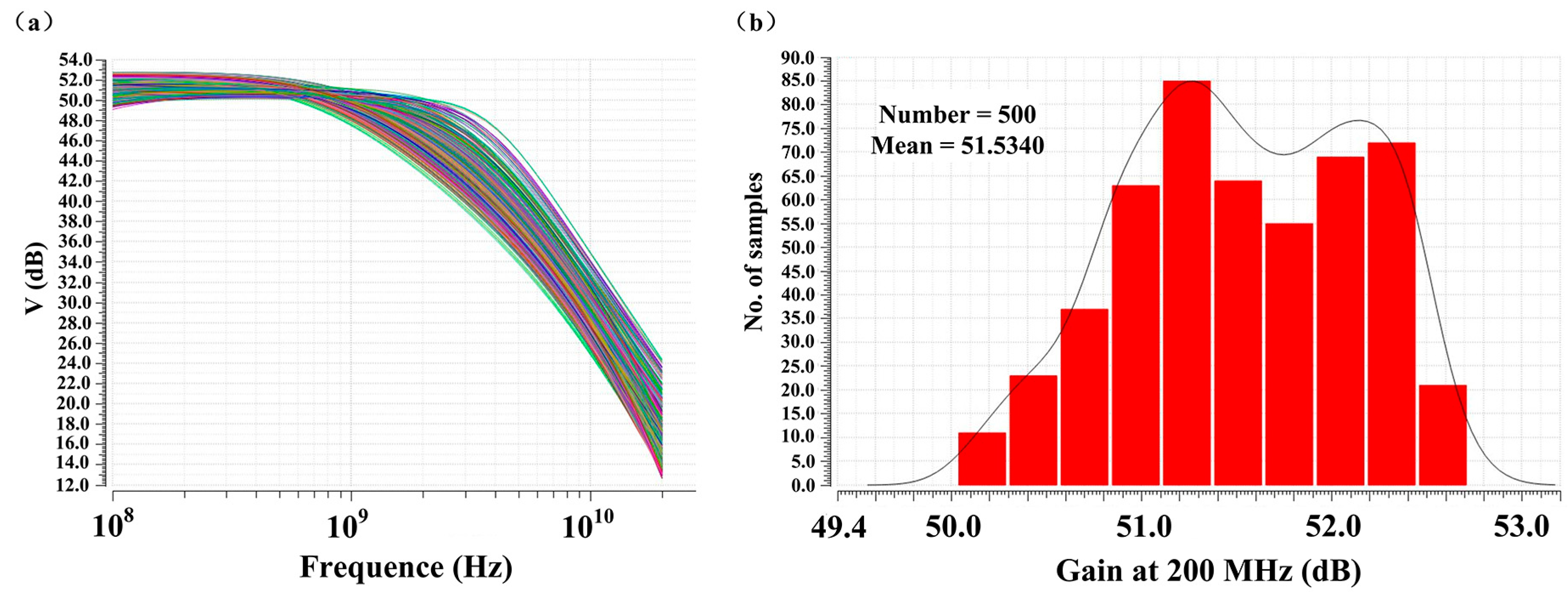
3.2. Simulation Results

The proposed TIA circuit is simulated with Cadence Spectre and a standard 65 nm CMOS process library. The amplitude–frequency characteristic curve is shown in Figure 7a. In a practical situation, the parasitic capacitance and resistance at the input are considered. Considering the possibility of producing a relatively extreme large input impedance, Rs and Cin at the input in Figure 6 are set at 5 kΩ and 200 fF. At this point, the value of the gain ZT shows an outstanding amplitude–frequency characteristic. The gain reaches 51.36 dB when the frequency is 200 MHz. And the −3 dB bandwidth of the curve is 1.3 Ghz. Thus, the circuit has a relatively large bandwidth, which means it can work well and maintain a high gain in high-frequency regions. This is important because according to Equation (2), when the circuit is adjusted to obtain a larger bandwidth, the input impedance can be effectively reduced so as to reduce the influence of a parasitic effect and large input impedance at the input. This effectively helps to solve the problem of a large impedance and parasitic effect generated from the sensing device.
Transient simulation results of TIA circuit are shown in Figure 7b. The input signals are set as sinusoidal current signals with swing amplitudes of 100 nA, 1 μ A, 10 μ A, and 100 μ A. The frequency is set to be 1 GHz for all of them. As can be seen from the figure, the voltage signal at the output is a sinusoidal wave with a phase opposite to the current signal at the input. For the input current at the μA level, the output voltage swing is at the mV level, and the amplification factor is about 49.31 dB after carrying out a calculation with the equation 20log( U o u t / I i n ), which is consistent with the result of 49.47 dB at 1 GHz in the AC simulation. For an input current of 100 nA, the output voltage swing is about 29.42 μ V, and the gain is 49.37 dB. It is found that even when the input current reaches the nA level, the circuit can still maintain a large gain and can amplify a small current into a large voltage without distortion. Through an analysis of the transient simulation results, it can be concluded that this TIA circuit solves the problem of a small input current.
At this point, the problems mentioned in the previous section are solved using the proposed TIA circuit. The output voltage with a large swing amplitude is transferred to the voltage comparison circuit of the next level, through which the high or low level is generated. It can be found that another advantage of using the TIA circuit is that voltage signals with a large swing amplitude can provide stable output results and avoid the wrong judgment coming from current signals with a small swing amplitude in current comparison circuits. In addition, the power consumption of the TIA circuit is 3.65 mW under the actual input conditions, which is relatively low. Monte Carlo simulation result of the amplitude-frequency characteristic with 500 calculations is shown in Figure 8a. And Figure 8b illustrates a Monte Carlo histogram distribution of the gain at 200 MHz. The histogram roughly presents the characteristics of a Gaussian distribution, and most of the simulation results for gain are concentrated between 51.2 dB and 52.4 dB. Monte Carlo simulation results with 500 calculations show that the gain curve is stable.

4. Conclusions

A new module for a magnetic induction switch is proposed. It is based on a sensing device made of a PM film and a current comparison circuit. The sensing principle, simulation results, and possible problems of the circuit are analyzed in detail. By introducing a newly designed TIA circuit to replace the current comparison circuit, a small current signal can be converted into a voltage signal with a large swing, and the voltage signal can then be easily handled in the following circuit. The whole circuit shows high gain, a huge bandwidth, and low power consumption. This outstanding performance helps solve the problems of a high input impedance, high frequency, and parasitic effect.

Author Contributions

Conceptualization, S.Z. and Y.J.; Formal analysis, S.Z.; Funding acquisition, S.Z.; Investigation, Q.J.; Methodology, S.Z.; Project administration, S.Z. and Y.J.; Resources, S.Z.; Software, Q.J.; Supervision, Y.J.; Validation, Y.J.; Writing—original draft, Q.J.; Writing—review & editing, S.Z. All authors have read and agreed to the published version of the manuscript.

Funding

This research was funded by the National Natural Science Foundation of China, grant number 62204100; the China Postdoctoral Science Foundation, grant number 2021M691360; and the Postdoctoral Research Foundation of Zhejiang Province, grant number ZJ2020101.

Data Availability Statement

Data are contained within the article.

Acknowledgments

Special thanks for technical support from the Department of Electronic Information and Control Engineering of the Beijing University of Technology.

Conflicts of Interest

The authors declare no conflicts of interest.

References

  1. Mishra, P.K.; Halavath, N.; Bhuktare, S. Strain-mediated voltage controlled magnetic anisotropy based switching for magnetic memory applications. J. Appl. Phys. 2023, 134, 123905. [Google Scholar] [CrossRef]
  2. Demirci, E. Magnetic and Magnetotransport Properties of Memory Sensors Based on Anisotropic Magnetoresistance. J. Supercond. Nov. Magn. 2020, 33, 3835–3840. [Google Scholar] [CrossRef]
  3. Liu, S.M.; Li, X.; Wang, Y.Q.; Yang, Y.F.; Meng, L.X.; Cheng, T.H.; Wang, Z.L. Magnetic switch structured triboelectric nanogenerator for continuous and regular harvesting of wind energy. Nano Energy 2021, 83, 105851. [Google Scholar] [CrossRef]
  4. Komine, T.; Chiba, T. Numerical analysis of voltage-controlled magnetization switching operation in magnetic-topological-insulator-based devices. Appl. Phys. Lett. 2023, 123, 102404. [Google Scholar] [CrossRef]
  5. Zhang, J.H.; Wang, Z.; Ma, C. A CMOS transimpedance amplifier with broad-band and high gain based on negative Miller capacitance. Integration 2023, 91, 60–66. [Google Scholar] [CrossRef]
  6. Costanzo, R.; Bowers, S.M. A Current Reuse Regulated Cascode CMOS Transimpedance Amplifier with 11-GHz Bandwidth. IEEE Microw. Wirel. Compon. 2018, 28, 816–818. [Google Scholar] [CrossRef]
  7. Fina, I.; Fábrega, L.; Martí, X.; Sánchez, F.; Fontcuberta, J. Magnetic switch of polarization in epitaxial orthorhombic YMnO thin films. Appl. Phys. Lett. 2010, 97, 232905. [Google Scholar] [CrossRef]
  8. Chen, W.Z.; Qian, L.J.; Xiao, G. Deterministic Current Induced Magnetic Switching Without External Field using Giant Spin Hall Effect of β-W. Sci. Rep. 2018, 8, 8144. [Google Scholar] [CrossRef] [PubMed]
  9. Wu, Y.; Hu, Y.; Wu, Y.F.; Rong, M.Z.; Yi, Q. Investigation of an Active Current Injection DC Circuit Breaker Based on a Magnetic Induction Current Commutation Module. IEEE T Power Deliv. 2018, 33, 1809–1817. [Google Scholar] [CrossRef]
  10. Wang, T.; Liu, S.; Zhou, Z.X.; Wang, W.Y.; Ren, S.Y.; Liu, B.L.; Gao, Z.X. Dual-responsive amplification strategy for ultrasensitive detection of norovirus in food samples: Combining magnetic relaxation switching and fluorescence assay. Sens. Actuat. B-Chem. 2023, 396, 134573. [Google Scholar] [CrossRef]
  11. Zhang, X.T.; Huang, H.N. Vehicle Classification Based on Feature Selection with Anisotropic Magnetoresistive Sensor. IEEE Sens. J. 2019, 19, 9976–9982. [Google Scholar] [CrossRef]
  12. Djuzhev, N.A.; Mazurkin, N.S.; Pozdnyakov, V.S.; Iurov, A.S.; Chinenkov, M.Y. Magnetic-field sensors based on anisotropic magnetoresistive thin-film structures for operation in a wide temperature range. Semicond 2015, 49, 1739–1742. [Google Scholar] [CrossRef]
  13. Zhang, S.S.L.; Vignale, G.; Zhang, S.F. Anisotropic magnetoresistance driven by surface spin-orbit scattering. Phys. Rev. B 2015, 92, 024412. [Google Scholar] [CrossRef]
  14. Volmer, M.; Neamtu, J. Magnetic field sensors based on Permalloy multilayers and nanogranular films. J. Magn. Magn. Mater. 2007, 316, E265–E268. [Google Scholar] [CrossRef]
  15. Belyaev, B.A.; Boev, N.M.; Izotov, A.V.; Skomorokhov, G.V.; Solovev, P.N. Magnetic Properties of Permalloy Thin Film Edges. Russ. Phys. J. 2020, 63, 16–22. [Google Scholar] [CrossRef]
  16. Wang, C.Y.; Su, W.; Hu, Z.Q.; Pu, J.T.; Guan, M.M.; Peng, B.; Li, L.; Ren, W.; Zhou, Z.Y.; Jiang, Z.D.; et al. Highly Sensitive Magnetic Sensor Based on Anisotropic Magnetoresistance Effect. IEEE Trans. Magn. 2018, 54, 2301103. [Google Scholar] [CrossRef]
  17. Ueki, R.; Okada, T.; Masuzawa, M.; Tsuchiya, K.; Kawamoto, T.; Utnemori, K.; Kako, E.; Konomi, T.; Sakai, H. Study on Magneto-Resistance Sensors for Low Magnetic Field Measurements. IEEE Trans. Appl. Supercond. 2020, 30, 9001204. [Google Scholar] [CrossRef]
  18. Romanova, A.; Barzdenas, V. On Noise Modeling of Capacitive Feedback Transimpedance Amplifiers in CMOS. Appl. Sci. 2022, 12, 10186. [Google Scholar] [CrossRef]
  19. Perelló-Roig, R.; Verd, J.; Bota, S.; Segura, J. A Tunable-Gain Transimpedance Amplifier for CMOS-MEMS Resonators Characterization. Micromachines 2021, 12, 82. [Google Scholar] [CrossRef] [PubMed]
Figure 1. (a) Measurement results of PM surface roughness. (b) Internal structure of WB.
Inventions 09 00004 g001
Figure 2. (a) Photograph of the packaged AMR sensor, (b) schematic of the PM strip, and (c) the current produced by a PM strip under the action of a magnetic field, changing alternately in two opposite directions along the Z-axis.
Inventions 09 00004 g002
Figure 3. Schematic of the proposed module with a current comparison circuit.
Inventions 09 00004 g003
Figure 4. (a) Schematic of current comparison circuit. (b) Transient simulation results of current comparison circuit.
Inventions 09 00004 g004
Figure 5. Schematic of the proposed module with a TIA circuit.
Inventions 09 00004 g005
Figure 6. Schematic of (a) a conventional RGC-TIA and (b) the proposed TIA.
Inventions 09 00004 g006
Figure 7. (a) Amplitude-frequency characteristic curve of the proposed TIA circuit, and (b) transient simulation results of proposed TIA circuit with different input currents.
Inventions 09 00004 g007
Figure 8. Monte Carlo simulation results of the proposed TIA circuit: (a) amplitude-frequency characteristic with 500 calculations. (b) histogram distribution of the gain at 200 MHz.
Inventions 09 00004 g008
Disclaimer/Publisher’s Note: The statements, opinions and data contained in all publications are solely those of the individual author(s) and contributor(s) and not of MDPI and/or the editor(s). MDPI and/or the editor(s) disclaim responsibility for any injury to people or property resulting from any ideas, methods, instructions or products referred to in the content.

