Article

Field-Programmable Analog Array Implementation of Neuromorphic Silicon Neurons with Fractional Dynamics

by
Andrés J. Serrano-Balbontín
*,
Inés Tejado
* and
Blas M. Vinagre
Escuela de Ingenierías Industriales, Universidad de Extremadura, 06006 Badajoz, Spain
*
Authors to whom correspondence should be addressed.
Fractal Fract. 2024, 8(4), 226; https://doi.org/10.3390/fractalfract8040226
Submission received: 1 March 2024 / Revised: 9 April 2024 / Accepted: 11 April 2024 / Published: 15 April 2024

Abstract

:
Silicon neurons are bioinspired circuits with the capability to reproduce the modulation through pulse-frequency observed in real neurons. They are of particular interest in closed-loop schemes to encode the control signal into pulses. This paper proposes the analog realization of neuromorphic silicon neurons with fractional dynamics. In particular, the fractional-order (FO) operator is introduced into classical neurons with the intention of reproducing the adaptation that has been observed experimentally in real neurons, which is the variation in the firing frequency even when considering a constant or periodic incoming stimulus. For validation purposes, simulations using a field-programmable analog array (FPAA) are performed to verify the behavior of the circuits.

1. Introduction

Neuromorphic engineering is a discipline inspired by the working principles of the biological nervous system to develop both hardware and software that are more efficient. Carver Mead, who believed that the brain could be at least 10 million times more efficient than digital technology [1], proposed analog silicon systems as the technology capable of imitating neural systems [2]. Examples of neuromorphic engineering include investigations into neuromorphic computing to develop new hardware technologies capable of mimicking the topology of the brain. In software, brain-inspired algorithms, such as artificial neural networks, have shown remarkable success [3].
Among the many areas of research in neuromorphic technologies, this work is inspired by the way in which biological neurons transmit information in the form of pulse trains. In particular, the concept of pulse-frequency modulation (PFM) emerged as an abstraction from the study of neuronal communication links in physiological control systems [4]. The application of PFM in current technologies has already provided the first fruitful results. For example, the use of PFM as a modulation technique for switching regulators has been shown to be more power efficient at low load conditions than other alternatives, such as pulse-width modulation (PWM), because it reduces the losses associated with the number of commutations [5]. In fact, switching regulators currently available on the market use a combination of these techniques.
In the field of control systems, the concept of neuromorphic control (NC) has recently emerged. It relies on neuron-inspired modulation techniques to encode the controller signal into pulses that mimic the operation of the biological motor system [6]. PFM provides robustness to noise because it encodes information in the distance between pulses rather than in amplitude. It has also been found to be particularly good at improving the precision of actuators, even in cases of poor behavior. For example, unlike PWM, PFM naturally handles static friction in DC motors because the energy delivered by each pulse can be tuned to overcome static friction at any time [6].
Silicon neurons are low-power circuits that reproduce the spike-based models of neurons and constitute the main building blocks for the implementation of neuromorphic systems. They are hybrid analog/digital very-large-scale integration (VLSI) circuits that emulate the electrophysiological behavior of real neurons and are suitable for implementing the real-time interaction of a neuromorphic system with its environment. There are many types of silicon neurons that vary in complexity depending on the application. In particular, biophysically realistic models that emulate the detailed internal dynamics of the neuron can be found in the literature, such as the Hodgkin–Huxley model as well as basic circuits that attempt to directly mimic the spike-like output of real neurons, such as integrate-and-fire (I&F) circuits [7]. This paper focuses on the latter. In this sense, a proposal for such a type of circuits is the fractional-order (FO) I&F neuron, which is able to model the firing frequency adaptation observed in real neurons to constant or periodic stimuli by introducing only one parameter, the order of the operator [8].
A field-programmable analog array (hereafter, FPAA) is an integrated circuit using switched capacitor technology that provides the ability to configure an analog signal processing system. The FPAA consists of an array of configurable analog blocks (CABs) that contain the resources to implement comparators, gain blocks, dividers, multipliers, filters, adders and subtractors, among other functions. FPAAs offer control designers new ways in simple and rapid verifying and prototyping of the analog implementation of controllers [9]. FPAAs take relevancy in the research of neuromorphic algorithms because they are the main alternative in the analog domain to digital prototyping with field-programmable gate arrays (FPGAs).
Recently, two applications related to the FPAA-based implementation of the FO operator have received much interest: FO chaotic systems and FO filters. With respect to the former, Charef’s approximation of the FO operator has been implemented in, e.g., [10,11,12]. For analog FO filters, the realization of the operator using partial fraction expansion (PFE), Oustaloup’s (in its classical and modified versions), Matsuda’s, and Charef’s methods can be found in [13]. Likewise, an implementation based on Oustaloup’s approximation combined with a curve-fitting-based method has been proposed in [14] for power-law filters (transfer functions raised to an FO) and using particle swarm optimization in [15]. A comparison study on the Carlson, continued fraction expansion, Padé, Charef, and curve-fitting approximation techniques can be found in [16]. The curve-fitting methodology is tested for double-order filters (FO filters raised to an FO) in [17].
To the best of the authors’ knowledge, there is only one paper that uses FPAAs to implement FO neurons. The type of neuron implemented there is known as the FitzHugh–Nagumo neuron, which is not expected to be used for signal modulation in control systems, but it has potential use in spiking neural networks [18].
This paper explores the functionality of the Anadigm® AN231E04 circuit for the analog implementation of silicon neurons and fractional operators, as well as their combination, for use in control applications. Three types of integer-order neurons are implemented in the FPAA, two of which are classical circuits that have been adapted to this technology, while the third is a neuron proposed here to perform PFM correctly. Three types of FO operator implementations are compared. Finally, FO variants of two different types of neurons are proposed based on our previous results. The Anadigm programming and simulation environment is used to verify the behavior of the designs.
After this introduction, Section 2 covers some basics about silicon neurons and the FO operator that are necessary for understanding the rest of the paper. Section 3 contains the description of the implementations of both the selected silicon neurons and the FO operator in the Anadigm FPAA. Section 4 shows and discusses the results obtained by simulating the proposed analog circuits. Conclusions are given in Section 5.

2. Fundamentals

This section contains the basics of biological neurons, PFM, silicon neurons by types, the FO operator, and fractional neurons.

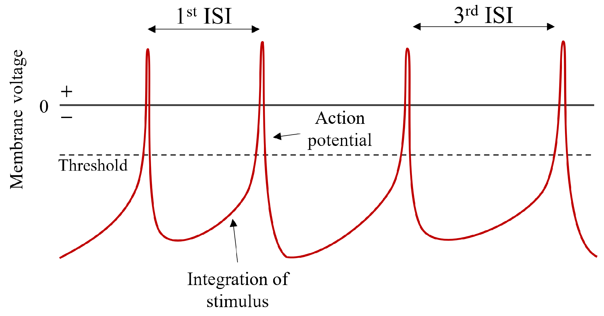
2.1. Biological Neurons

Real neurons transmit information in the form of spikes called action potentials. Evolution has found this type of representation to be more efficient and reliable for transmitting information compared to continuous signals [6]. At rest, the cell membrane has a negative polarization. An incoming stimulus causes the depolarization, which is an increase in the membrane voltage. The summation of these stimulus-induced depolarizations is also known as integration. When a threshold is reached, a positive feedback loop is activated, causing the neuron to depolarize even more. When the peak is reached, the membrane voltage returns to the negative resting state. This short upward and downward variation in the membrane voltage is the action potential. As action potentials do not change their shape, information is conveyed in the timing of action potentials. The elapsed time between action potentials is known as the inter-spike interval (ISI). Figure 1 shows the evolution of membrane voltage in a neuron.

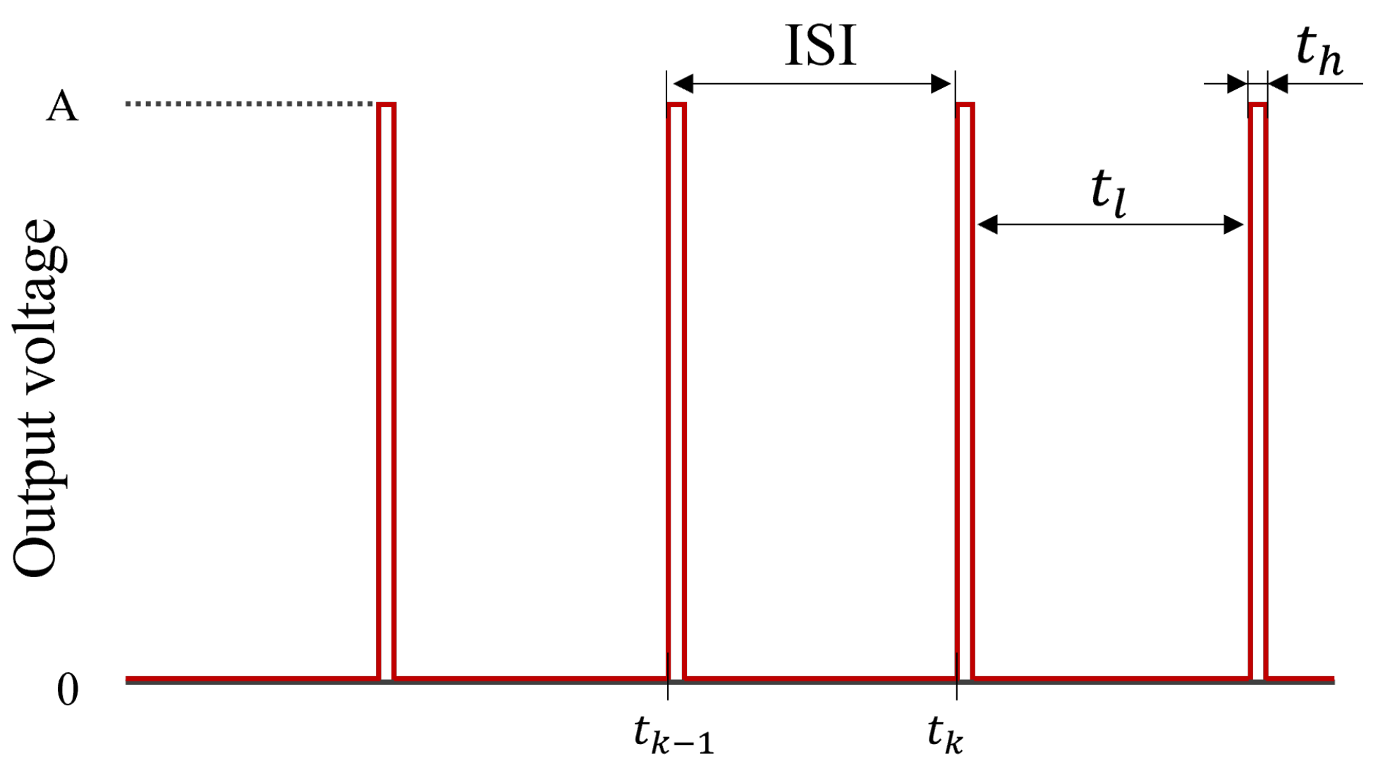
2.2. Pulse-Frequency Modulation

PFM originated as a modulation technique inspired by the output of biological neurons. The amplitude information of the input signal is encoded in the spacing between impulses or pulses of constant width [4]. Therefore, the output can be represented as a succession of pulses:
z ( t ) = A k 1 δ ( t t k )
where z ( t ) is the output of the PFM, A is the amplitude of the pulses, δ is the Dirac delta function or unit impulse, and t k is the instant at which the k-th pulse is fired. For PFM that fires pulses with non-zero width, i.e., rectangular pulses, the output is described by:
z ( t ) = A k 1 θ ( t t k ) θ ( t t k t h )
where t h is the width of the pulse or high state duration, and θ is the unit step function. The time between pulses also satisfies t h + t l = t k t k 1 , where t l is the duration of the low state. A representation of the output is depicted in Figure 2. The most common PFM variant, and the one closest to biological behavior, is the integral PFM (IPFM) [19], which determines the firing instant t k by integrating the input until a certain amount K t i , called threshold, is reached, i.e.,
y ( t k ) = t k 1 t k x ( t ) d t = K t i
where x ( t ) and y ( t ) are the integrator input and output, respectively. After each pulse is fired, the integral is reset, which is denoted by:
y ( t k + ) 0
Traditionally, neuron models have only considered positive inputs, leading to the concept of single-signed IPFM (SS-IPFM), which includes a rectifier at the input to avoid negative values ( x ( t ) 0 ), as shown in Figure 3.

2.3. Silicon Neurons

Silicon neurons, also called just neurons, are circuits that use the silicon medium to reproduce the dynamics of real neurons. There is a wide variety of silicon neurons whose structure depends on the application and the fidelity to reproduce the different dynamics of real neurons.

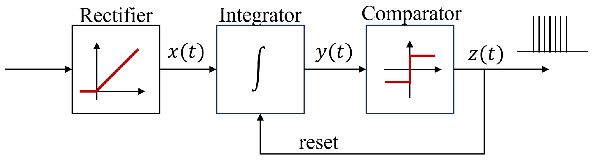
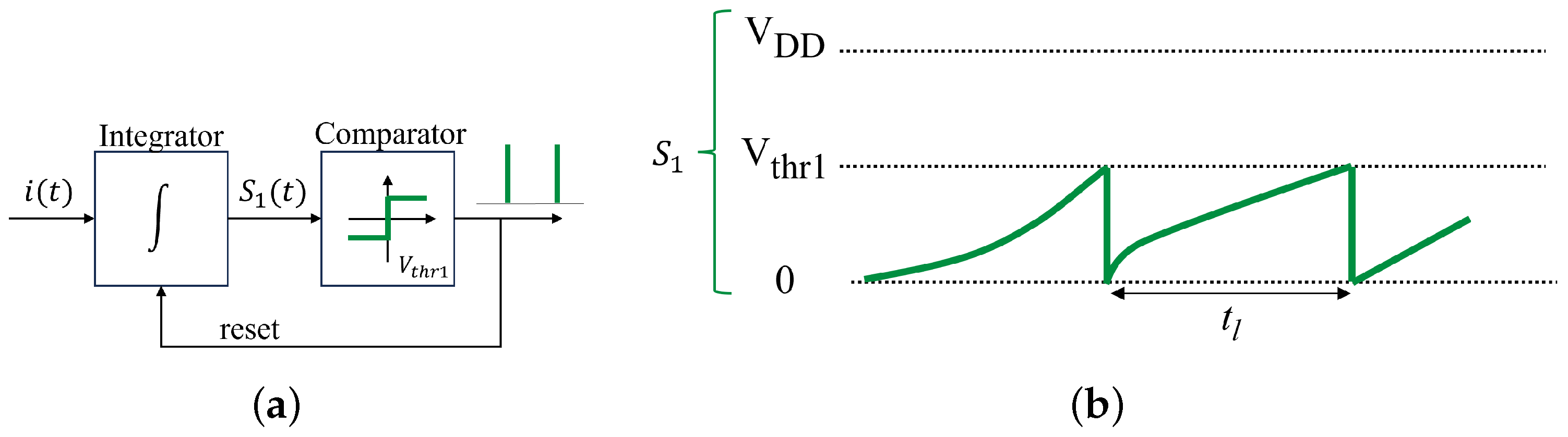
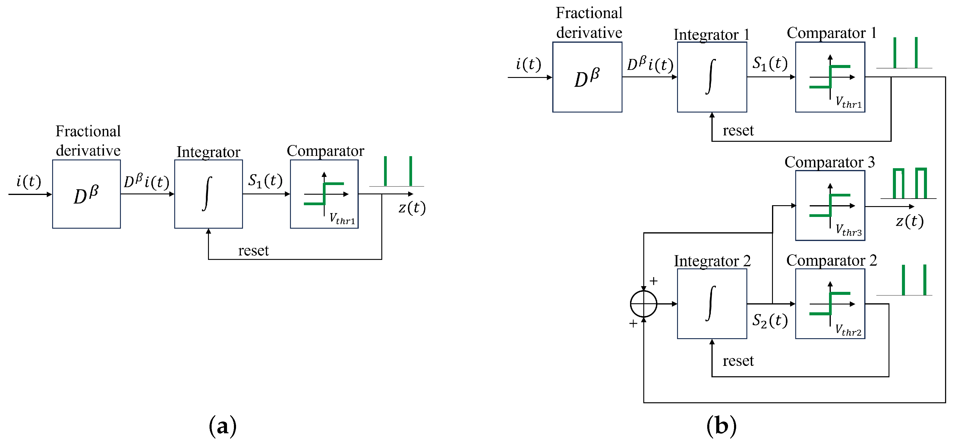
2.3.1. Integrate-and-Fire Neurons

Early designs of silicon neurons were used to mimic the firing frequency of real neurons by simply using a resistor–capacitor (RC) circuit, leading to the concept of I&F neuron models [20]. I&F neurons have, at least, the following four properties: (1) a threshold is set; (2) the input is integrated, usually using a capacitor; (3) a spike is fired when the integration reaches the threshold; and (4) the neuron returns to the resting state to begin another cycle, which is usually performed either by a shortcut between the ends of the capacitor or by feeding a negative input. These are the common approaches, but there are infinite cases. It is important to clarify the difference between I&F and IPFM concepts. I&F encompasses a wide variety of integration and firing processes that model neuron behavior where the input–output relationship may be nonlinear. In contrast, IPFM uses a specific integration and firing process, which was originated as a modulation technique, where the dependence of the average output on the average input must be linear. Appendix A includes an explanation on how to relate IPFM to other neuron models. The simplest I&F circuit consists of a single capacitor, as shown in Figure 4a. It is charged by a positive input current and can be reset by connecting a switch in parallel. Each time the voltage reaches the threshold, a spike is fired by a secondary circuit, Θ, and the neuron is reset by a brief commutation of the switch. Note that, in contrast to the biological dynamics of membrane voltage, the integration and generation of pulses (representing action potentials) are separated. The voltage evolution in the capacitor is given by the following two equations:
V A ( t k ) = 1 C m t k 1 t k i ( t ) d t = V t h r
V A ( t k + ) 0
where C m is the membrane capacitance, i ( t ) is the instantaneous current through the capacitor, V A ( t ) and V t h r are the voltage across the capacitor and the voltage threshold, respectively, t k is the instant at which the k-th pulse is triggered, and V A ( 0 ) = 0 denotes the initial condition. In this case, (3) and (4) are imitated by this simple circuit. It is worth mentioning that constants C m and V t h r can be combined in a single threshold K t i , A with the value K t i , A = C m V t h r .

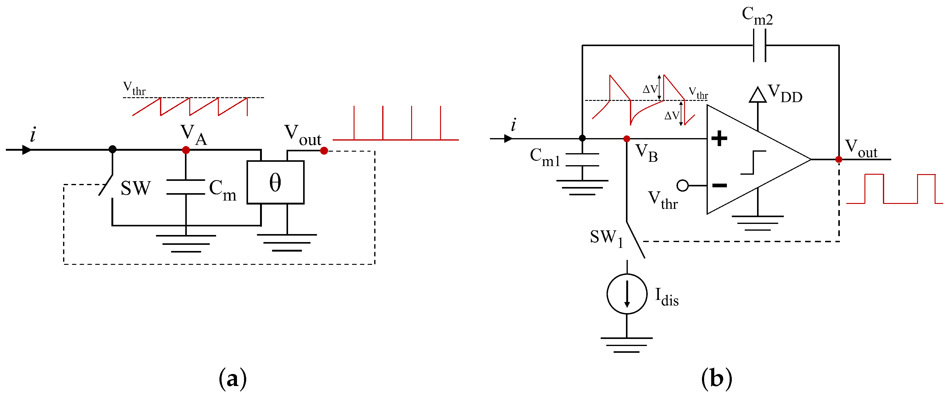
2.3.2. Axon-Hillock Circuit

The Axon-Hillock (A-H) circuit is the evolution of the first I&F models, resulting in one of the simplest implementations of a silicon neuron for rectangular pulse generation. The circuit (Figure 4b) comprises the input current, a positive feedback loop created by an amplifier and two capacitors that form a capacitive voltage divider, and a constant discharging current controlled by a switch. It was used for control purposes in [6]. Its output is determined by an integration at two different rates around a threshold, i.e., the integral is not reset to zero. First, the integral V B ( t ) of the input signal is performed until the threshold V t h r is reached, which provides the time to the first pulse. Second, the circuit adds an offset Δ V to the integral ( Δ V = V D D C 2 / ( C 1 + C 2 ) ; expression derived from the capacitive voltage divider) and the input signal is replaced by a negative constant input until the threshold is reached again, but from above, which determines the width of the pulse. Third, the same offset is subtracted from the integral and the integration of the input is started again for the next low duration. The variation of the integral signal V B ( t ) is illustrated in Figure 5. This circuit is valuable because it is compact, consumes low power, and uses asynchronous strategies to determine the time in the high state. More details about the analog implementation of this circuit and its variants can be found in [2,7].
The evolution of V B ( t ) , after reaching the threshold the first time, is determined by the following set of equations:
V B ( t ) = V t h r Δ V + 1 C B t k 1 + t h t i ( t ) d t if V B ( t ) < V t h r V B ( t k + ) V t h r + Δ V if V B ( t k ) = V t h r V B ( t ) = V t h r + Δ V 1 C B t k t I d i s d t if V B ( t ) > V t h r V B ( ( t k + t h ) + ) V t h r Δ V if V B ( t k + t h ) = V t h r
where C B is the parallel of capacitors C m 1 and C m 2 , and I d i s is the discharging current. Also, C B and Δ V can be combined in a single threshold K t i , B with the value K t i , B = C B Δ V . The output is described by:
z B ( t ) = A if V B ( t ) V t h r 0 if V B ( t ) < V t h r
With regard to an A-H neuron, it is important to remark the following issues:
  • It does not actually implement IPFM, but something that is very close to it, for narrow pulse widths. Therefore, in the next section, a new type of neuron capable of performing PFM is proposed and compared to the A-H neuron.
  • It cannot be directly reproduced in the FPAA because individual electronic components cannot be used. However, CABs, which can implement integrators and comparators, are available in an FPAA and can be used to mimic the input-to-output behavior based on analog principles. Having a quickly configurable neuron could help to verify designs prior to the final fabrication of the silicon neurons.

2.4. Fractional Operator

The Riemann–Liouville definition for the FO derivative of order α [ 0 , 1 ] is defined as follows:
D α f ( t ) = 1 Γ ( 1 α ) d d t 0 t f ( τ ) ( t τ ) α d τ = f ( t ) t α Γ ( 1 α )
where Γ and * denote the Gamma function and the convolution operation, respectively. In this definition, the FO derivative of a constant is not equal to zero, which can be observed in the power-law decaying kernel. Its Laplace transform for zero initial conditions can be expressed as:
L { D α f ( t ) } = s α F ( s )
The Oustaloup approximation, also known as the Oustaloup recursive method, consists of the product of pairs of poles and zeros to approximate the FO operator, D α , with α 1 , 1 , as follows:
s α C 0 k = 1 N s + ω z k s + ω p k
where ω z k and ω p k are the frequencies of the zeros and poles, respectively, N is the order of the approximation, and C 0 is a constant. This approximation is valid in the range [ w b , w h ] , where ω b and ω h are the low and high transition frequencies, respectively. The correct gain at 1 rad/s, which is | ( j ω ) α | = 1 , can be adjusted by C 0 , but if 1 rad/s is outside of [ w b , w h ] , the gain can be adjusted at any other suitable frequency instead [21].
This approximation can also be expressed using PFE as the sum of first order transfer functions and a constant, i.e.,
s α c 0 + i = 1 N c i T i s + 1
where c 0 , c i , and T i are constants.

2.5. Fractional-Order Integrate-and-Fire Neurons

Recently, new models of silicon neurons using FO operators have emerged to model the spike frequency variation, also known as adaptation or accommodation, observed in some types of real neurons in response to constant or periodic stimuli. Integer-order models predict that, for this kind of input, the spikes should follow a uniform pattern over time. In [8], an FO model was utilized to describe experimental data where adaptation was relevant. It is thought that these dynamics can provide neurons with additional mechanisms for the transmission of information, such as
C f D α V f ( t ) = i ( t )
where α 0 , 1 in this case, and C f and V f are the capacitor and the voltage in this fractional model, respectively.

3. Analog Implementation
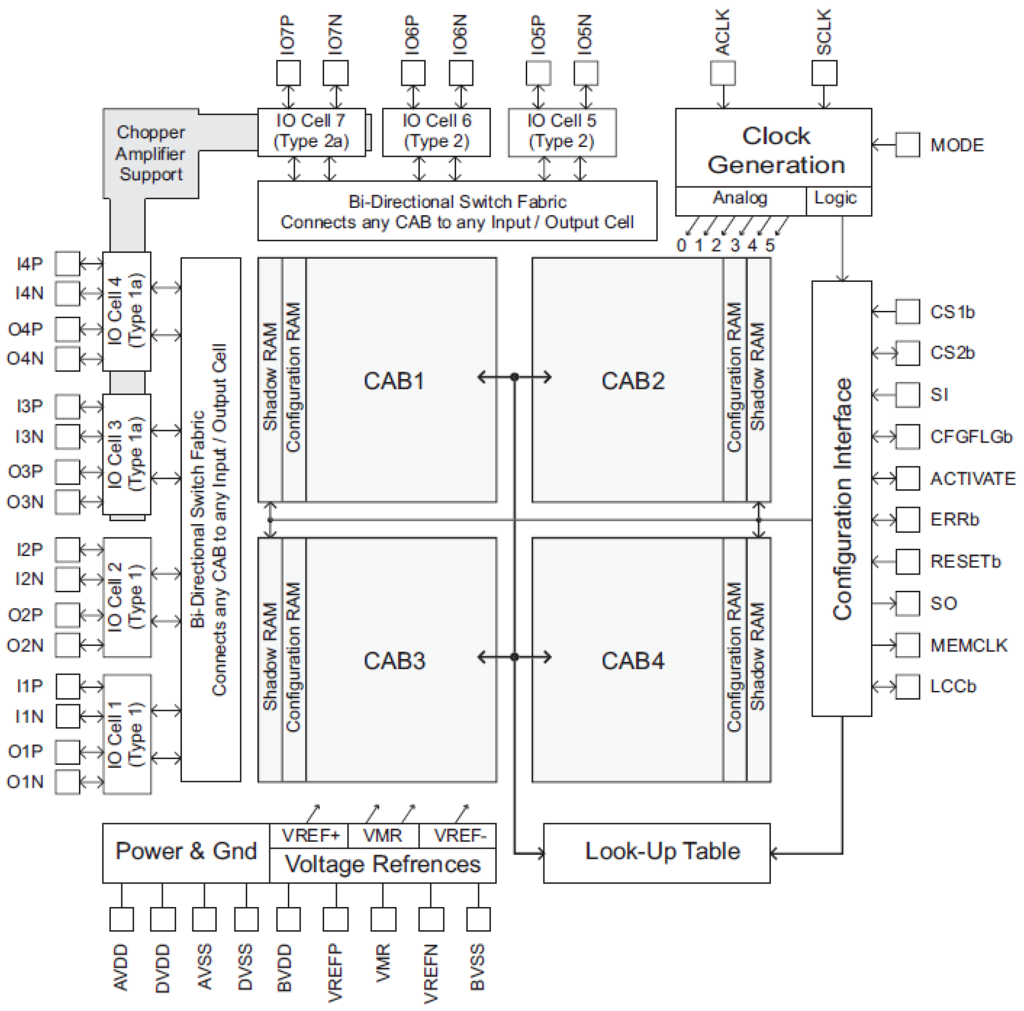
This section addresses the analog implementation of the silicon neurons considered in this work using the AN231E04 FPAA from Anadigm®. Firstly, details of the FPAA are given from both hardware and software perspectives. Then, the implementation of the neurons are presented based on the description in Section 2.

3.1. Anadigm’s FPAA

The AN231E04 device is one of the dynamically reconfigurable FPAAs in the family of integrated circuits offered by Anadigm®. It consists of, depending on the development kit, one, two or four FPAA modules. Each FPAA has seven analog input/output (I/O) cells and four configurable blocks. Every CAB contains two op-amps, a comparator, banks of programmable capacitors, and a collection of configurable routing and clock resources. For complex signal processing, it is common to connect several FPAAs together. Its architecture is illustrated in Figure 6. Configuration data are stored in an on-chip static random access memory (SRAM) and configuration can be changed dynamically.
FPAA programming is carried out with the AnadigmDesigner2 software, a visual programming environment using high level block diagrams. The FPAA modules are represented as subsystems, while each circuit function is represented by blocks denominated configurable analog modules (CAMs), which are made up by the resources available from CABs. CAMs must be connected by wires, making up a schematic. In this environment, it is possible to deal with continuous or sampled signals. When the labels Φ 1 and Φ 2 appear next to a pin, it indicates that the corresponding input of that CAM is sampled on phase 1 or 2, respectively, with respect to its own CAM clock, while for output pins, it indicates that the output changes only during the specified phase and is held or set to zero during the opposite phase, also referred to as half-cycle signals.
The relevant considerations related to the analog processing of signals derived from its architecture are summarized next:
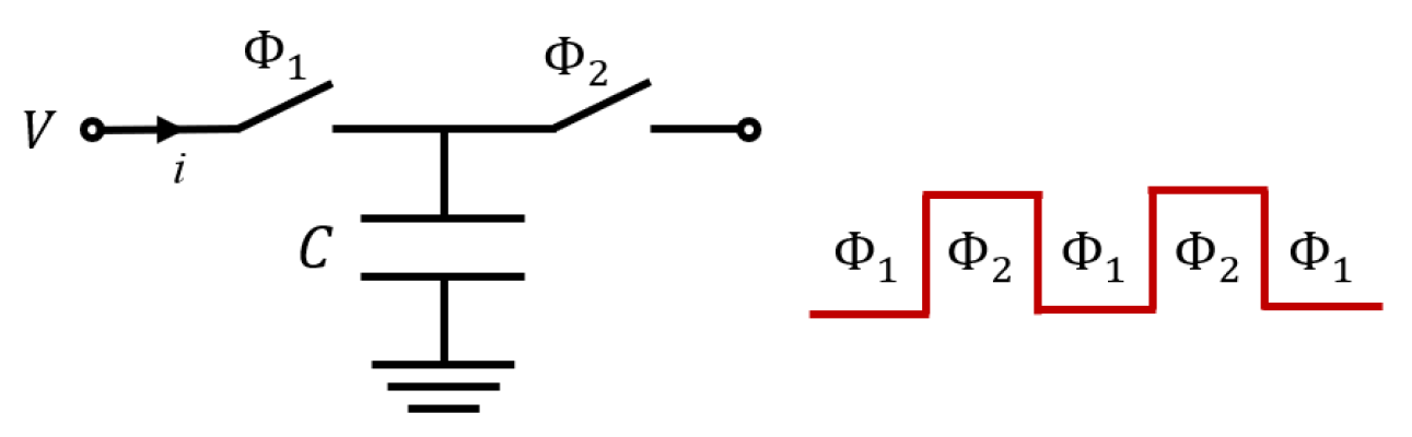
  • The FPAA uses switched capacitor technology, which mimics the behavior of other components, such as resistors, by controlling the current flowing to or from capacitors. Figure 7 illustrates the concept. One consequence is that the values of the parameters of a CAM are quantized and limited to a frequency-dependent range. It also causes some CAM signals to be sampled in one of two non-overlapping phases of the clock, while others are processed in continuous time. Therefore, the clock frequency and the phase in which the signal is processed affect the design process. Continuous-time CAMs are preferred when possible.
  • The FPAA operates internally with differential signals centered around a mid-rail voltage (VMR) of 1.5 V, which is the internal signal reference. Therefore, the common mode voltage of the signals is 1.5 V. The differential mode ranges from −3 to +3 V. Both differential and non-differential signals can be connected to the FPAA. In the case of non-differential ones, the negative pin is connected to VMR.
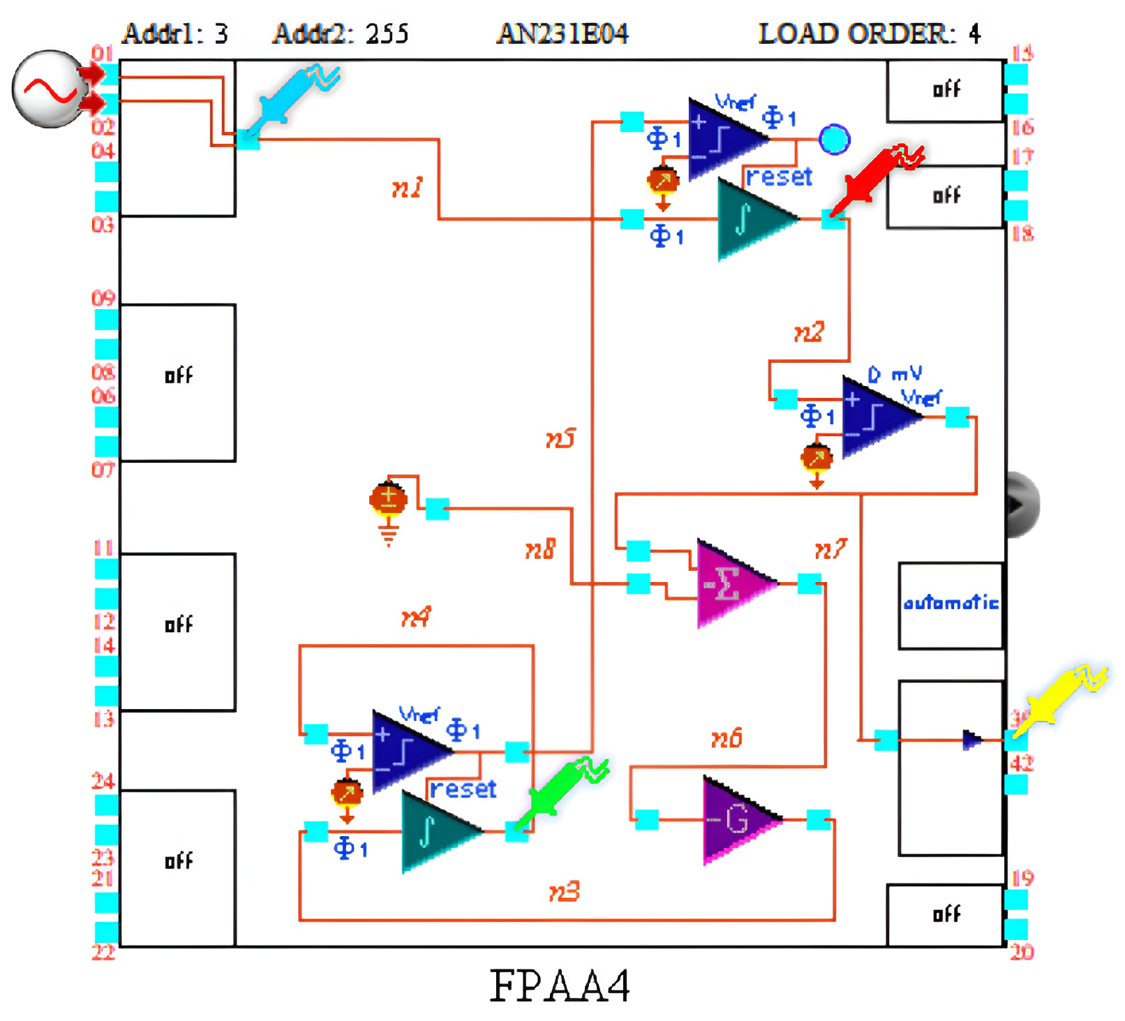
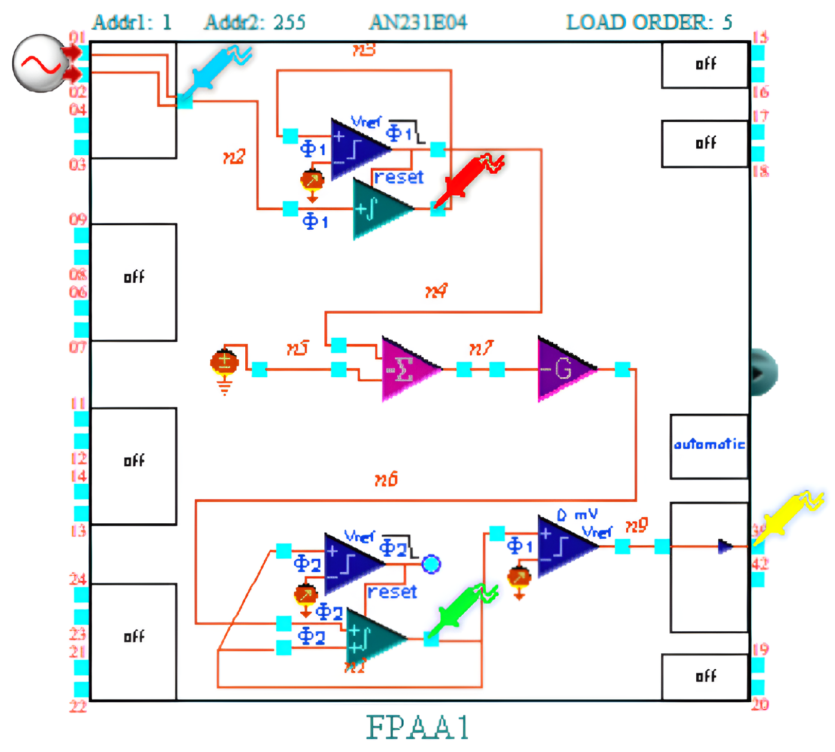
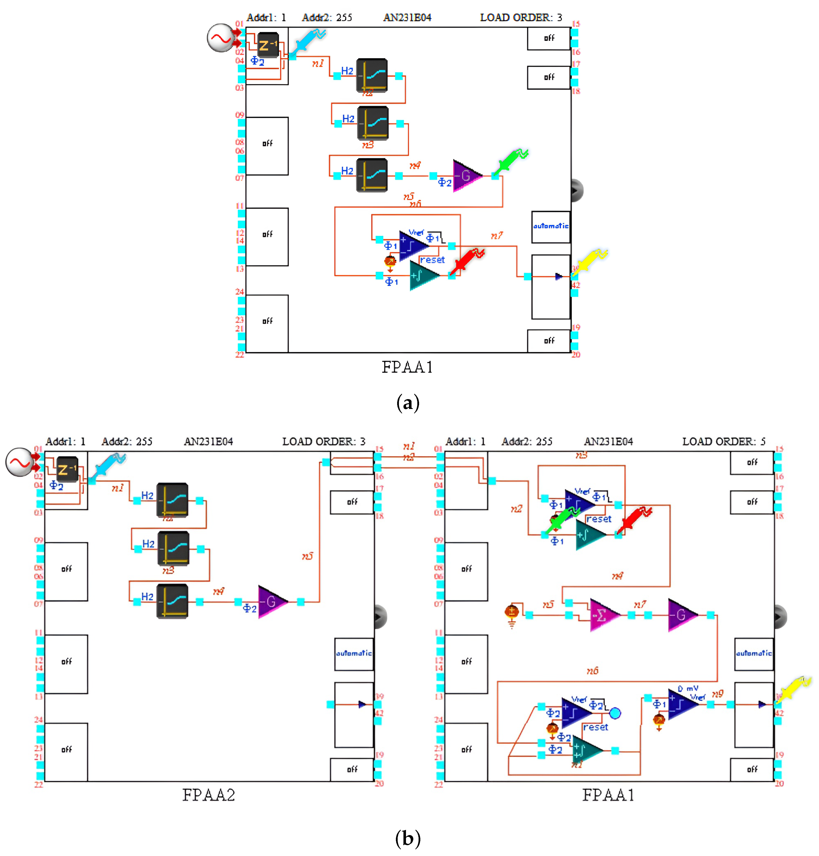
  • The CAMs can be configured as: (a) Integrators and SumIntegrators, which are single-input and two- or three-input integrators, respectively, with integration constants programmable for each input (on the scale of µs−1) and with an optional reset function controlled by a comparator that is part of the same CAM; (b) Comparators, which produce digital output levels that go high when the input is greater than an internal programmable reference or an external signal; (c) FilterBilinears (BFs), which can be programmed as low-pass, high-pass, and all-pass filters or as zero-pole pairs; (d) GainInv and GainHold, which are the continuous-time and half-cycle gains, respectively; and (e) SumInv and SumDiff, which are the continuous-time and half-cycle summing blocks, respectively, with three and four possible inputs, respectively. CAMs are typically recommended to have a clock frequency of 4 MHz or less, with the exception of comparators, which can be used at 8 MHz. Here, the highest clock frequency will be used to achieve neuron behaviors closer to pure analog versions, i.e., closer to mimicking asynchronous strategies.

3.2. Integer-Order Neurons

The proposed implementations of neurons in the FPAA are now explained. In particular, three types of integer-order neurons are considered.

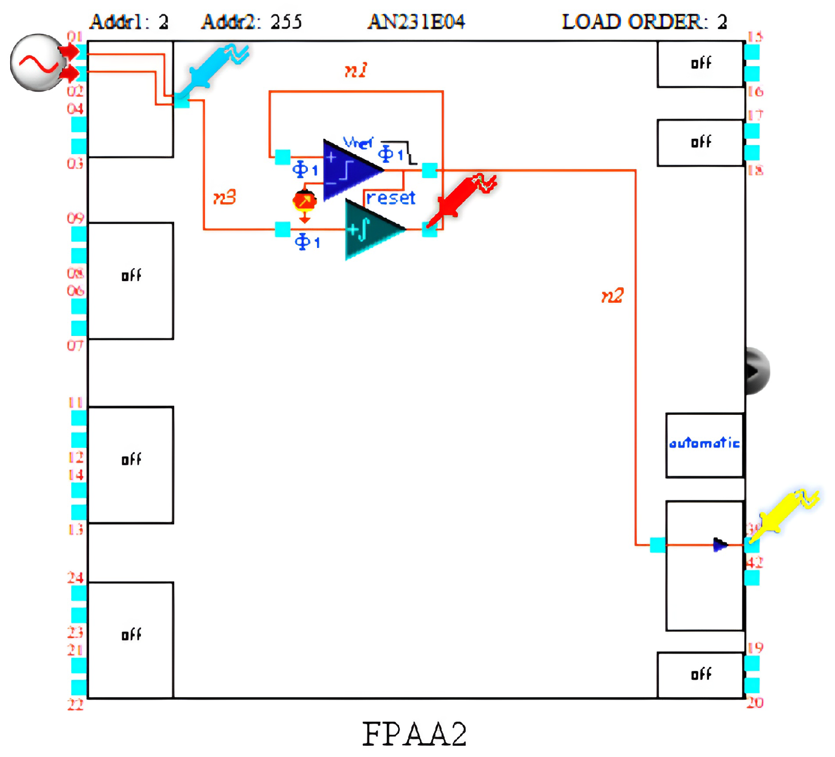
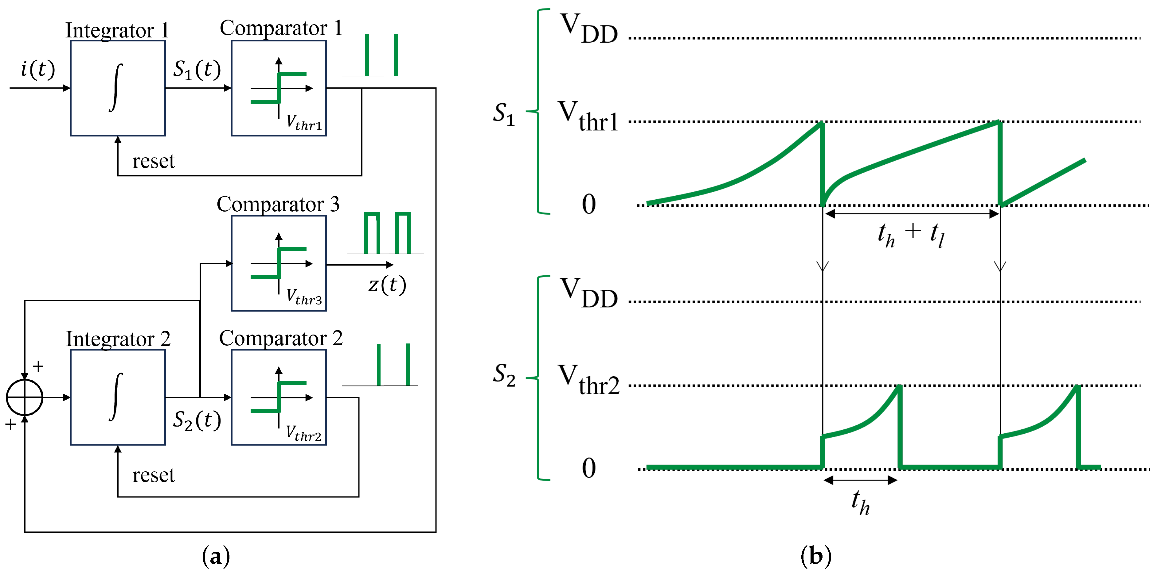
3.2.1. Dirac Delta-Pulsed Neuron

The simplest implementation of an I&F neuron with an impulse-like output of the form of (1) is achieved by reproducing (5) and (6) directly, which involves only one integral with reset and a comparator. Figure 8a shows the block diagram of this neuron (DP neuron, hereafter), whereas Figure 8b illustrates the evolution of the integrator output. V D D = 3 V denotes the maximum voltage of the signals within the FPAA. From now on, i ( t ) will represent the input in terms of voltage since it is the working domain of the FPAA, and, for simplicity, only positive inputs are considered ( i ( t ) 0 ).
In the FPAA, an integrator block with reset option controlled by a comparator signal fits the requirements. Figure 9 shows the schematic of this implementation in the AnadigmDesigner2 software. As can be seen, a single FPAA is employed. A wave generator is connected as input to pins 01 and 02 (top-left corner). The output of the integrator will be fed to the input of the comparator, whereas the output of the comparator will be the impulse-like output. Actually, it is a pulse of 250 nanoseconds when using a 4 MHz clock in the CAM ( f s = 4 MHz). The output of the comparator is routed to an I/O cell in order to make it accessible outside the FPAA (pin 39). Since all comparators of the CAMs are either 2 or + 2 V in differential mode internally, the I/O cell has been set to work in “comparator mode”, which converts a comparator signal to a single-ended signal outside the FPAA, between 0 and 3.3 V. The probes in the schematic indicate which signals of the simulation will be plotted. Only the pulse train of the neuron is measured outside the FPAA because it is the main signal. The intermediate signals, such as integrator output, are testing points, i.e., signals to monitor the circuitry behavior. Measuring them outside requires using additional resources. Furthermore, it is easier to interpret the differential signals inside the FPAA than the two-pin signals outside the FPAA.
Mathematically, the behavior is described by:
S 1 A ( t ) = τ 1 A i ( t ) d t
S 1 A ( t k + ) 0 if C 1 A ( t k ) = + V C
C 1 A ( t ) = + V C if S 1 A ( t ) > U 1 A V C if S 1 A ( t ) U 1 A
where S 1 A ( t ) and C 1 A ( t ) are the output of the integrator and the comparator, respectively, V C = 2 V and U 1 A and τ 1 A are the configurable parameters in the CAM, namely, the comparator threshold and the constant of integration, respectively. Comparing this implementation with the IPFM theoretical model, the following relation can be obtained:
K t i A = U 1 A τ 1 A
where K t i A is the equivalent threshold.

3.2.2. Axon-Hillock-Like Neuron

One way to generate an output similar to that of the A-H circuit in the FPAA is to use two integrators with reset. The proposed implementation is based on the following operating principles: (1) the input is integrated ( S 1 ) up to the threshold of the neuron ( V t h r , 1 ) and it is not yet reset but is ignored (it is ignored as in the A-H circuit); (2) when the threshold is reached, a second integral ( S 2 ) with constant input is activated, which will determine the time in the high state; (3) when the threshold of the second comparator ( V t h r , 2 ) is reached, both integrals are reset to start a new cycle; and (4) the signal S 2 is fed to a comparator to obtain the output pulses. An illustration of the block diagram of the implementation and the evolution of both integrals S 1 and S 2 are shown in Figure 10a and Figure 10b, respectively. The first integrator output, S 1 , replicates the behavior of V 1 ( t ) in the A-H circuit (Figure 4b) during the low state (i.e., V 1 < V t h r ), while the second integrator output, S 2 , reproduces it during the high state (namely, V 1 > V t h r ).
Having sketched the general idea, the schematic used to reproduce the neuron behavior is illustrated in Figure 11. It can be observed that it contains two integrators with reset, an independent comparator, a voltage source (+2), an inverting gain, and an inverted summing block. Its description is as follows. The first integrator block (top) receives the input signal i ( t ) from the wave generator and integrates it until the pulse has been released, i.e.,
S 1 B ( t ) = τ 1 B i ( t ) d t
S 1 B ( ( t k + t h ) + ) 0 if C 1 B ( t k + t h ) = + V C
C 1 B ( t ) = + V C if C 2 B ( t ) > U 1 B V C if C 2 B ( t ) U 1 B
where S 1 B ( t ) is the output of the first integrator block, C 1 B ( t ) and C 2 B ( t ) are the output of the comparators of the first and the second integrator blocks (the latter, at the bottom), respectively, and U 1 B is the threshold of the comparator of the first integrator block. The activation of the input of the second integrator block and, therefore, the trigger of a pulse, is given by the independent comparator with output C 3 B ( t ) (middle right):
C 3 B ( t ) = + V C if S 1 B ( t ) > U 3 B V C if S 1 B ( t ) U 3 B
where U 3 B is the threshold of this comparator, which is, in fact, the neuron threshold V t h r , 1 .
In order to take only the positive part of this comparator output, a constant voltage of 2 V is added by using the voltage block (middle left), the inverted summing block, and the inverting gain (bottom right). Taken together, these three blocks act much like a half-wave rectifier ( R 1 B ( t ) ). Note that a half-wave rectifier block was not used instead because it was observed to cause significant distortion in the dynamics. Therefore, the output of this set of blocks is:
R 1 B ( t ) = + V D D if C 1 B ( t ) > 0 0 if C 1 B ( t ) 0
The second integrator block receives the rectified signal and integrates it until it reaches its own threshold, i.e.,
S 2 B ( t ) = τ 2 B R 1 B ( t ) d t
S 2 B ( ( t k + t h ) + ) 0 if C 2 B ( t k + t h ) = + V C
C 2 B ( t ) = + V C if S 2 B ( t ) > U 2 B V C if S 2 B ( t ) U 2 B
where S 2 B ( t ) and U 2 B are the output and the threshold ( V t h r , 2 ) of the second integrator with reset block, respectively. Finally, the single-ended output of this schematic is obtained by feeding an I/O cell, operating in comparator mode, with the output C 3 B ( t ) (similar to the previous implementation).
The properties of the output pulses can be described by the following expressions:
t l B = U 3 B τ 1 B i ¯
t h B = U 2 B τ 2 B V D D
where i ¯ can be a constant input or the average value of i ( t ) over the time interval in which it participates ( t l B in this case). This model is related to the A-H model as follows:
K t i B = U 3 B τ 1 B
I d i s B = V D D U 3 B U 2 B τ 2 B τ 1 B
By making U 2 B = U 3 B , more similarity to an A-H neuron can be achieved. The value of threshold U 1 B is chosen to reset the integrators S 1 B and S 2 B at the same time (e.g., U 1 B = 0 ).

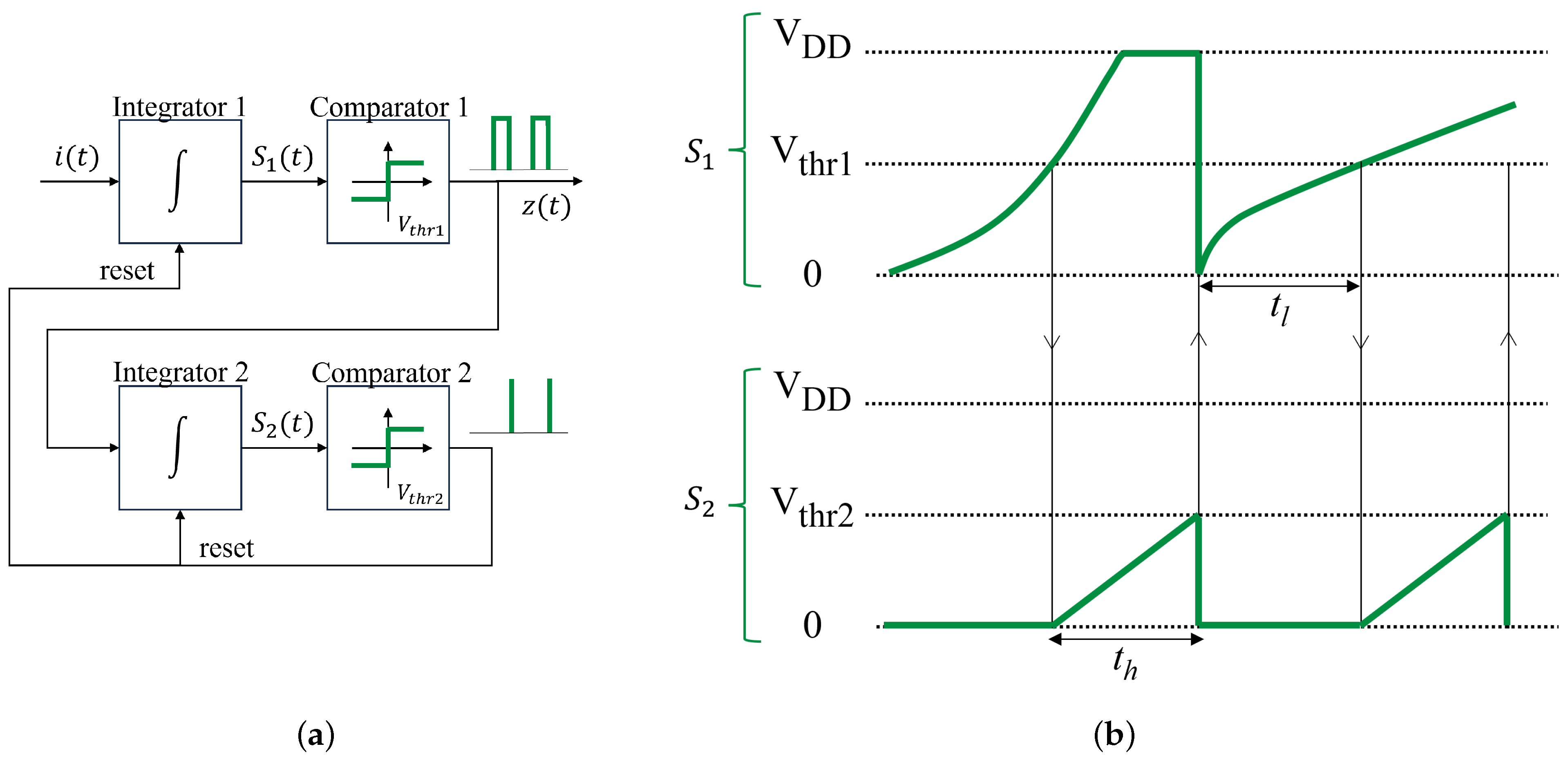
3.2.3. True-PFM Neuron

An alternative to the previously presented schematic to perform correct PFM modulation is what we call the true-PFM (TPFM) neuron, which operates as follows. First, the input ( S 1 ) is integrated up to the threshold ( V t h r , 1 ) and immediately reset (similar to the delta-pulsed neuron). Then, a positive feedback involving a second integrator ( S 2 ) starts the integration when the impulse of the previous integrator is received. The positive feedback stops when the threshold of the second integrator ( V t h r , 2 ) is reached, which determines the high state duration. Note that real neurons use positive feedback to generate action potentials. Finally, the output S 2 is given as input to a third comparator to obtain the rectangular output pulses ( V t h r 3 close to 0). Figure 12a shows the block diagram of the neuron, while Figure 12b illustrates a possible scenario for the evolution of the two integrals.
The proposed implementation for the FPAA contains an integrator block, a summing integrator block, two independent comparators, an inverted summing stage, and an inverted gain, as shown in Figure 13. The first integrator with reset, which behaves as a DP neuron, is described by:
S 1 C ( t ) = τ 1 C i ( t ) d t
S 1 C ( t k + ) 0 if C 1 C ( t k ) = + V C
C 1 A ( t ) = + V C if S 1 C ( t ) > U 1 C V C if S 1 C ( t ) U 1 C
The output signal of the comparator C 1 A is processed with a rectifier similar to the previous implementation. The combined output of the blocks is then:
R 1 C ( t ) = + V D D if C 1 C ( t ) > 0 0 if C 1 C ( t ) 0
The integrator–adder block receives the rectified delta pulse from the first integrator block and its own output, forming a positive feedback. The duration in the high state is determined by the time it takes for the integral to integrate the sum since the delta pulse is triggered until it reaches the threshold of its comparator:
S 2 C ( t ) = ( τ 2 , 1 C R 1 C ( t ) + τ 2 , 2 C S 2 C ( t ) ) d t
S 2 C ( ( t k + t h ) + ) 0 if C 2 C ( t k + t h ) = + V C
C 2 C ( t ) = + V C if S 2 C ( t ) > U 2 C V C if S 2 C ( t ) U 2 C
where τ 2 , 1 C and τ 2 , 2 C are the integrator–adder block gains. Thus, the second integral follows a differential equation of the form:
d d t S 2 C ( t ) = τ 2 , 2 C S 2 C ( t ) + τ 2 , 1 C V D D δ ( t t k ) , S 2 C ( 0 ) = 0
whose solution is:
S 2 C ( t ) = τ 2 , 1 C V D D e τ 2 , 2 C ( t t k ) θ ( t t k )
Note that (37) and (38) are simplifications in which a single pulse has been considered to facilitate the following deductions. In particular, at the moment when the integral reaches the threshold U 2 C , the following holds:
S 2 C ( t k + t h ) = τ 2 , 1 C V D D e τ 2 , 2 C t h = U 2 C
Since the maximum value of U 2 C is V D D , τ 2 , 1 C must be less than 1. From (39), the following expression is deducted for the high state duration:
t h C = 1 τ 2 , 2 C ln U 2 C τ 2 , 1 C V D D
while the elapsed time between pulses is the same as in the DP neuron, i.e.,
I S I k = t l C + t h C = U 1 C τ 1 C i ¯
The equivalent threshold, K t i C , is obtained as:
K t i C = U 1 C τ 1 C
Table 1 contains a comparison of the three implementations of integer-order neurons, namely DP, A-H, and TPFM neurons.

3.3. Fractional-Order Operator

Figure 14 shows the schematics used to implement the FO operator in AnadigmDesigner2. Based on the two forms of the approximation of the FO operator (i.e., transfer functions (11) and (12)), three different implementations are developed:
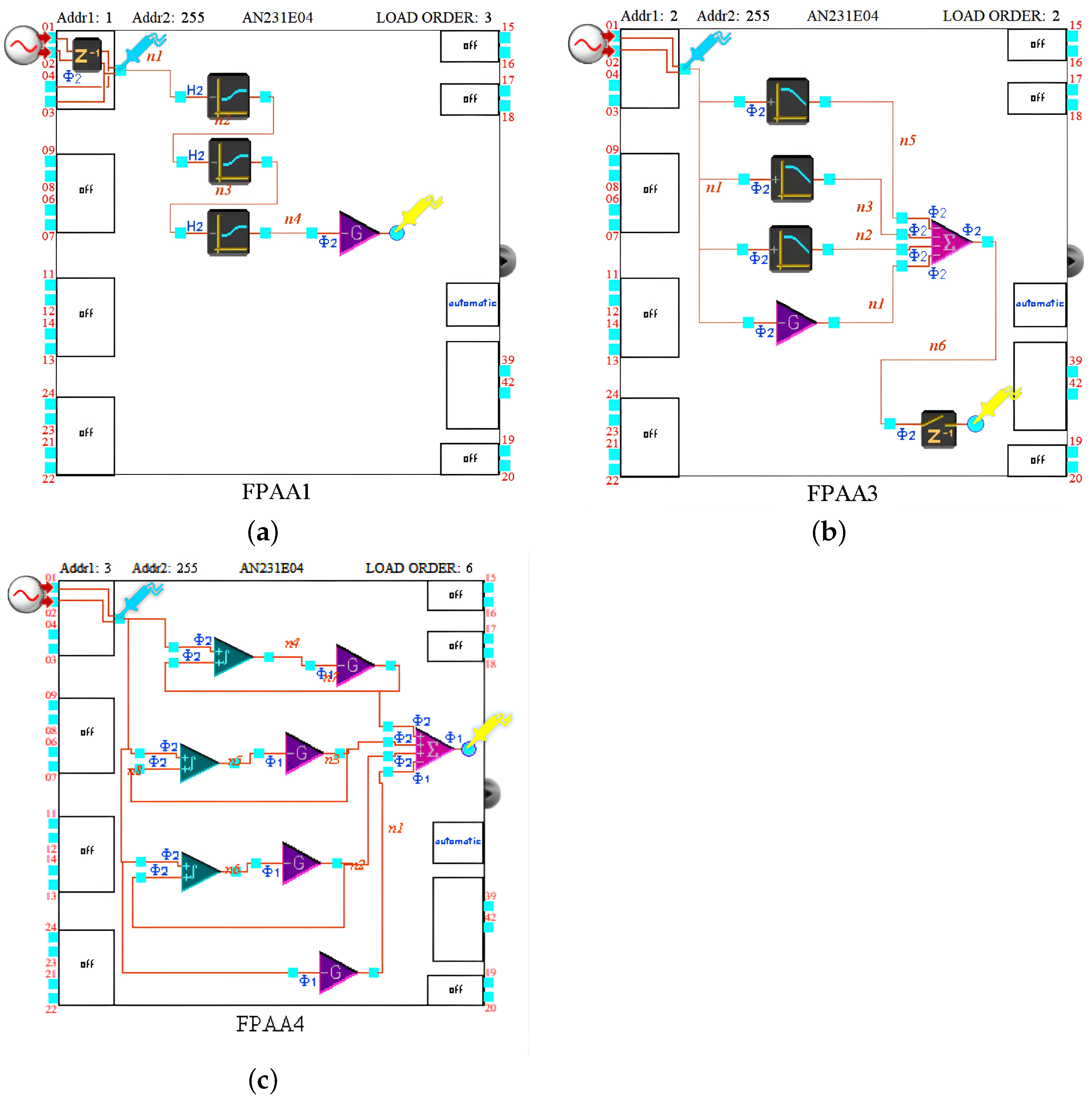
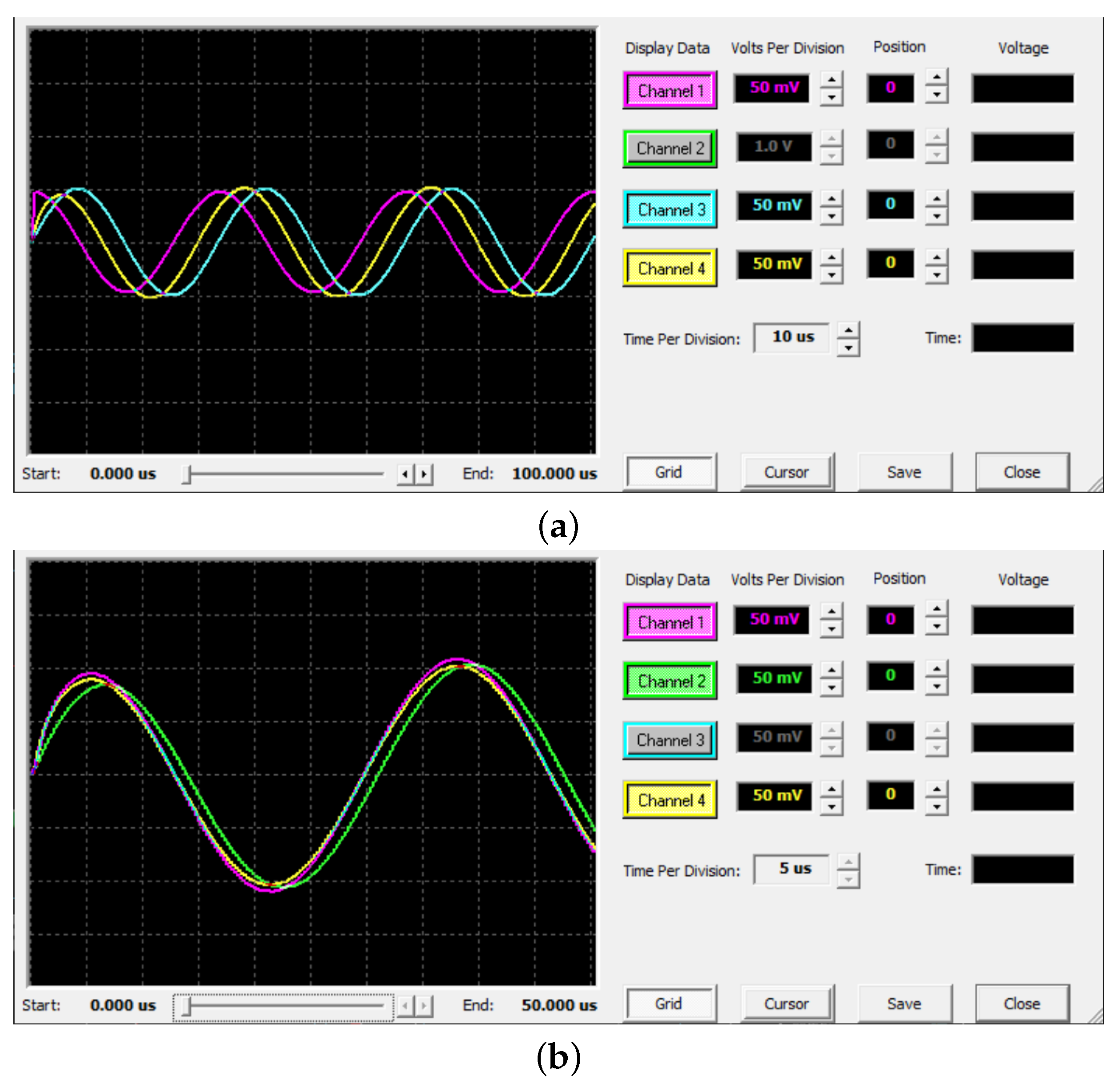
  • Setting up the BFs as zero-pole pairs in series to match transfer function (11), similar to [23]. This implementation will be referred to as BFs in series. Each of these CAMs has the following transfer function:
    V o u t ( s ) V i n ( s ) = G H F s + 2 π f z s + 2 π f p
    where G H F is the gain at high frequencies, and f z and f p are the zero and pole frequencies, respectively, with the condition:
    G D C = f z f p G H F
    where G D C is the static gain. In this form, the number of BFs required is equal to the order of the approximation to match the number of poles and zeros. Because the BFs have an inverted output, when dealing with an odd approximation order, an inverted gain must be connected to achieve a non-inverted operator. To implement the constant C 0 of (11), its value can be distributed among the BFs gains and/or the additional inverting gain. Furthermore, as recommended in the documentation, the I/O cell is configured as an input with sample and hold that samples during phase 2. Figure 14a shows the implementation for this case for an approximation of order three (i.e., N = 3 ).
  • Using the BFs as low-pass filters, along with summing blocks and a gain, to obtain transfer function (12). This implementation will be referred to as BFs in parallel. Each of these CAMs has the following transfer function:
    V o u t ( s ) V i n ( s ) = ± 2 π f 0 G s + 2 π f 0
    where f 0 is the corner frequency, and G is the gain. The CAM output can either be inverted or non-inverted. To implement the FO operator in the PFE form, the number of BFs required is equal to the order of the approximation in order to match the number of poles. The corner frequency in each CAM is chosen to be equal to each pole frequency ( f 0 i = ( 2 π T i ) 1 ), while G is used to adjust the filter gain ( G i = c i ), where subscript i denotes each zero-pole pair of the approximation. The constant c 0 is implemented as a gain block and it is added to the BF outputs thanks to the summing blocks. When using half-cycle summing blocks, the output is held using a sample and hold block or I/O cell configured as output with sample and hold. In Figure 14b, the schematic of this implementation is illustrated again for an approximation of order three.
  • Using individual integrators and gains to assemble low-pass filters and thus transfer function (12), similar to [24]. This implementation will be referred to as individual integrators. Each negative loop making up the low-pass filter has the following transfer function:
    V o u t ( s ) V i n ( s ) = G τ 1 s + G τ 2
    where τ 1 and τ 2 are the constants of the integration of the individual integrator, and G is the value of the gain connected to it. The number of loops required is equal to the order of the approximation, i.e., N integrators and N gains. The integration constants are chosen to satisfy G τ 2 = T i 1 , and τ 1 τ 2 1 = c i (again, subscript i denotes the pairs zero-pole of the approximation). The constant c 0 is implemented through an additional inverting gain. The loop outputs and the constant c 0 are added by using summing blocks. The schematic of this implementation is shown in Figure 14c also for an approximation of order three.
It is important to highlight that the implementation using BFs in series requires fewer resources than the other two alternatives considered. This is because it does not require summing blocks, resulting in a decrease in the number of CAMs used and, consequently, in power consumption. Additionally, the free FPAA components could be utilized for other tasks. However, in terms of versatility, the third option, individual integrators, may be more suitable. In contrast to the use of BFs, where the placement of poles and zeros is directly determined by the sampling frequency of the CAM, the poles in the third form are linked to the values of the integration constants and the gain. This feature allows for a wider frequency range in which the approximation of the FO operator is valid and for placing the band limits with less dependence on the sampling frequency.

3.4. Fractional-Order Neurons

Many papers on fractional I&F neurons can be found in the technical literature. However, most of them are limited to the calculation of the mathematical equations and do not deal with their analog implementation. Usually, the memory of the FO operator is preserved during the operation of the neuron because it is computed separately, i.e., the so-called memory trace is guaranteed [8,25]. In these works, the adaptation is observed to have two properties at the output for a constant input: (1) the firing frequency decreases or increases with time, and (2) the baseline frequency depends on the FO operator. The existing works dealing with the analog implementation of FO neurons fail to achieve real adaptation because they use an FO integrator that loses memory as soon as it is reset after firing a pulse, as shown, for example, in [26]. Although the firing frequency is observed to depend on the FO operator, the first property is not achieved.
Here, to solve this issue, the combination of classical integer- and fractional-order operators is used. In particular, the FO operator of order β = 1 α is added to the block diagram of each integer-order neuron before the first integrator for two purposes: (1) to allow the reset of the neuron by means of the integer-order integral (local operator), and (2) to preserve the dynamic memory (non-locality by time) thanks to the unaltered FO derivative. Therefore, the proposed FO-I&F neuron is ruled by:
y ( t k ) = t k 1 t k D β i ( t ) d t = K t i f
where D β is the FO operator of order β in the Riemann–Liouville sense, taking advantage of the non-zero derivative of a constant. After each pulse is fired, only the integer-order integrator is reset, which is denoted by:
y ( t k + ) 0
Among all the silicon neurons, two types were chosen, namely DP and TPFM cases, which will be referred to as FO-DP and FO-TPFM, respectively. This selection was based on the fact that the A-H neuron does not correctly modulate its input for wide pulses, and for thinner pulses, similar results would be expected. The analog implementation of an FO version of the A-H neuron can be found in our previous work [27], where simulation results in the MATLAB/Simulink environment are given to show its behavior. Figure 15 show the block diagrams of FO-DP neurons and FO-TPFM neurons based on this idea.
To implement the FO neurons in the FPAA, the FO operator is connected to an integer-order neuron in order to reproduce (47). The FO operator can be implemented by one of the previously presented forms. However, it is worth mentioning that the implementation of the FO operator using BFs in series is considered to be more appropriate for its use in NC systems because the limited resources are efficiently employed and can be freed for the controller itself and for other signal processing. The schematics in AnadigmDesigner2 corresponding to the FO-DP and FO-TPFM neurons are shown in Figure 16a and Figure 16b, respectively.

4. Results

This section contains the simulation results corresponding to the analog schematics presented earlier, obtained using the AnadigmDesigner2 software.

4.1. Integer-Order Neurons

The three types of integer-order neurons implemented in Section 3.2 (namely, DP, A-H, and TPFM) were tested for a constant input equal to 0.1 V. The parameters of the first integrator and the corresponding firing threshold in each implementation were chosen to be the same, i.e.,: τ 1 A = τ 1 B = τ 1 C = 0.2 µs−1, and U 1 A = U 3 B = U 1 C = 0.2 V. For the A-H and TPFM neurons, the parameters were selected to obtain a pulse width of t h B = t h C = 5 µs. Therefore, τ 2 B = 0.06 µs−1, U 1 B = 0 V, U 2 B = 0.9 V, τ 2 , 1 C = 1 µs−1, τ 2 , 2 C = 0.303 µs−1, and U 2 C = 3 V (see Appendix B for additional considerations in parameter selection).
The simulation results obtained are shown in Figure 17. They are visualized in the oscilloscope of AnadigmDesigner2, which can display a maximum of four signals simultaneously, corresponding to one probe per channel (CH). On the right side, the volts and time per division can be adjusted, as well as the position offset. The lower left corner shows the start and end times of the simulation. In particular:
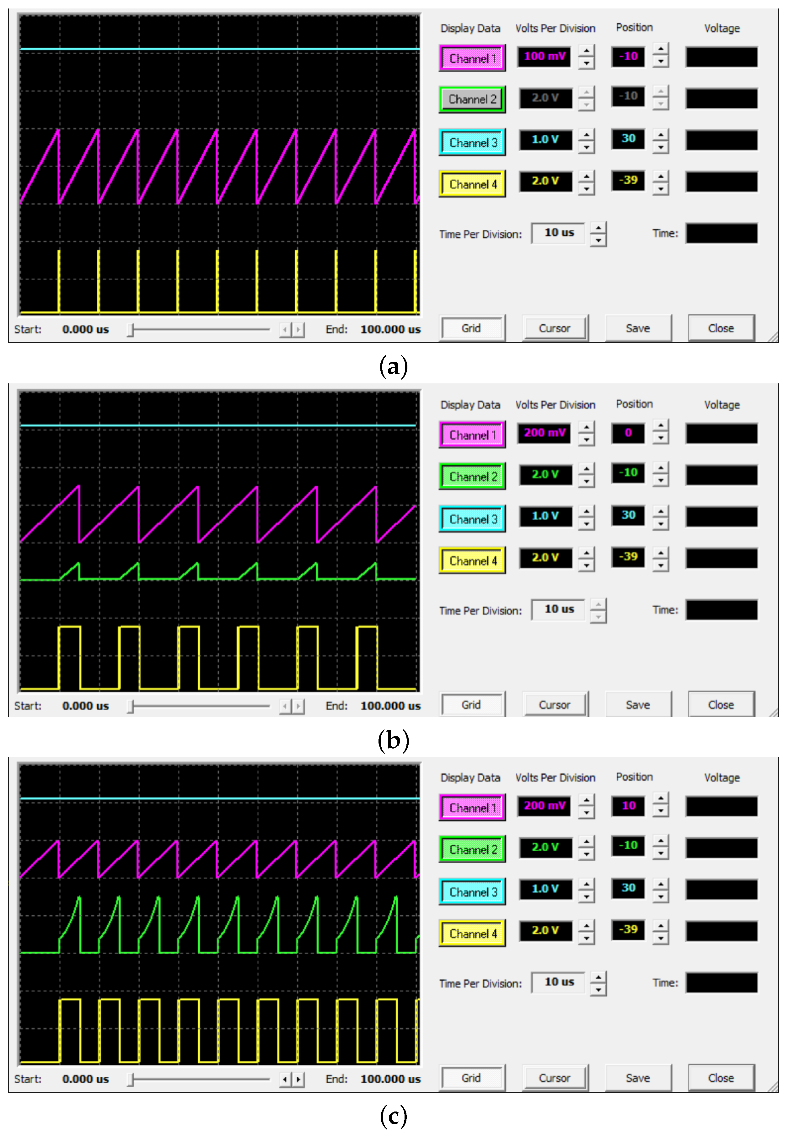
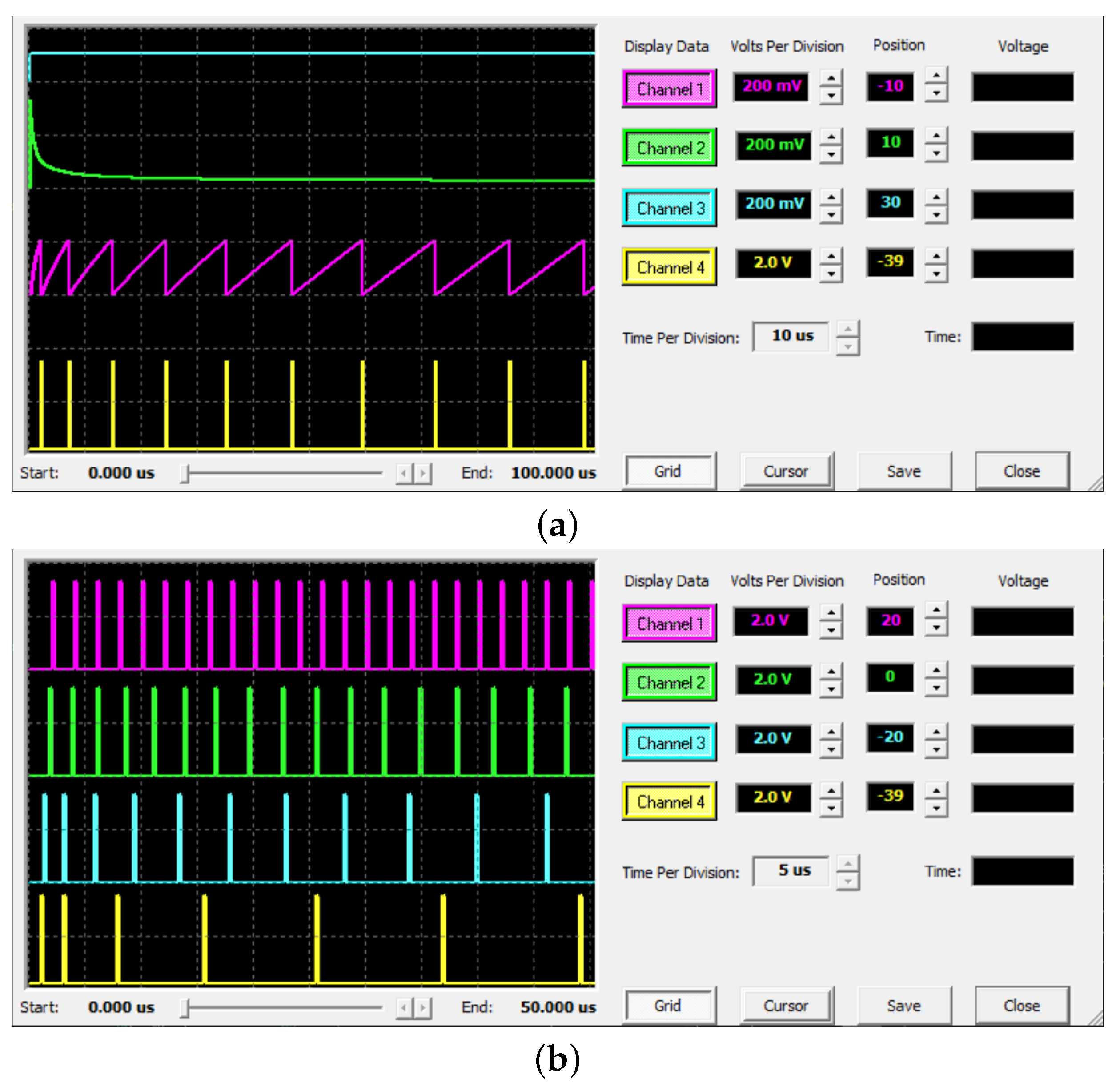
  • Figure 17a shows the signals of the DP neuron, consisting of the input (CH3), the integrator output (CH1), and the pulse train output (CH4). In CH1, the integral starts at 0 and integrates the input up to the selected threshold (namely, 200 mV), causing a pulse to be fired, as seen in CH4. The integral is then reset and a new cycle begins. This behavior causes the integral to appear as a sawtooth wave, and a uniform firing pattern is observed at the output.
  • Figure 17b corresponds to the A-H neuron. The plotted signals are the input (CH3), the integrator output (CH1), the integral in the high state (CH2), and the output pulses (CH4). The integral of the input differs from that of the DP neuron in that it reaches 200 mV and starts the second integration in CH2, but it is not reset. In fact, it is observed that the integral reaches almost 400 mV. The second integral that was initiated integrates at a constant rate until it reaches 0.9 V, the threshold chosen to obtain a pulse width of 5 µs. In CH4, the pulses coincide in time with the CH2 triangles. The obtained pulses have a width of 5 µs, as desired.
  • Figure 17c illustrates the results for the TPFM neuron, namely the input (CH3), the integrator output (CH1), the positive feedback involving the second integral (CH2), and the output pulses (CH4). It is observed that the signal in CH2 behaves like that of the DP neuron by resetting the integral at 200 mV. In CH3, the positive feedback is initiated each time that CH1 reaches the threshold, with a shape reminiscent of a slice of an exponential as derived in (38). The output fires pulses of width 5 µs in CH4. The main difference between the A-H and TPFM neurons is observed at the output: although the pulse width is the same, the firing frequency is not. The TPFM preserves the firing frequency of the DP neuron when using the same ‘equivalent threshold’ K t i and just adds more width to the pulse (causing the gain of the neuron to increase). However, the firing frequency of the A-H neuron decreases compared to the other two types because the integrator is ignored during the high state, resulting in delayed firing. The firing frequency does not depend linearly on the input amplitude, and, therefore, the A-H neuron does not modulate the input properly. As mentioned earlier, the differences are reduced for narrow pulses. Note that the duration of the first low state is longer than the successive ones caused by an initialization.

4.2. Fractional-Order Operator

Once the neuron implementations were observed to behave as desired, the next step was to validate the FO operator implementations. For illustration purposes, an FO operator of order 0.5 was considered for a sinusoidal input with a frequency of 30 kHz and an amplitude of 50 mV. The parameters used to obtain the Oustaloup approximation for the BFs in series and BFs in parallel were N = 3 , f b B F = 2 kHz, and f h B F = 400 kHz, which are the minimum and maximum frequencies available to place poles and zeros in these CAMs running at 4 MHz. For the implementation using individual integrators, an approximation of the same order ( N = 3 ), but with f b I I = 63.66 Hz, and f h I I = 4 kHz, which were chosen based on the frequency-dependent range limits of the integration constants of integrator blocks and gains when running the CAMs at 4 MHz. This range was selected to show the versatility of this implementation. The transfer functions of the approximations are:
H B F ( s ) = 3.76 ( s + 1.954 × 10 4 ) ( s + 1.143 × 10 5 ) ( s + 6.683 × 10 5 ) ( s + 4.730 × 10 4 ) ( s + 2.763 × 10 5 ) ( s + 1.616 × 10 6 )
H I I ( s ) = 1.2 ( s + 6.843 × 10 2 ) ( s + 5.861 × 10 3 ) ( s + 5.020 × 10 4 ) ( s + 2.002 × 10 3 ) ( s + 1.715 × 10 4 ) ( s + 1.469 × 10 5 )
where H B F denotes the transfer function for implementations using BFs, i.e., BFs in series and BFs in parallel, and H I I , corresponds to individual integrators. The parameters used in the CAMs for each implementation are listed in Table 2. Note that, for individual integrators, the magnitude was adjusted to obtain the same operator gain as in the other cases, at the same frequency ( f c = ( f b B F f l B F ) = 28 kHz), by using the gain of the summing block ( G S ).
The three types of analog implementations of the FO operator are compared in Figure 18. In particular, Figure 18a shows the input signal in CH3, together with its integer-order derivative in CH1 and the output (i.e., fractional-order derivative) in CH4 for the case where BFs are used in series. As can be observed, the FO derivative of s 0.5 causes the wave to be delayed almost π / 4 rad with respect to the input, while the integer derivative produces π / 2 rad as expected. In Figure 18b, the FO operator using BFs both in series (CH4) and in parallel (CH1) and that using integrators and gains (CH2) are plotted. Regarding the first two, it can be seen that there are only small differences in the performance of such implementations. However, the implementation using BFs in series requires fewer CAMs. Concerning the third one, a similar performance is observed for a single frequency, but, in contrast to the use of BFs, the working range of the approximation is between 63.6 Hz and 40 kHz. Likewise, it is observed that the phase is slightly different from the previous cases because of the range of the approximation, and, therefore, the phase at the given frequency changes. The primary disadvantage is that it consumes more resources compared to BFs in series.

4.3. Fractional-Order Neurons

After verifying that both the neuron and the FO operator functioned correctly, their combination was evaluated as an FO neuron. The simulation results obtained in AnadigmDesigner2 with such FO neurons are described next. In both cases, a constant voltage of 100 mV was considered as the input signal.
First, the simulation of the FO-DP neuron is described. The neuron parameters were τ 1 A = 0.6 µs−1 and U 1 A = 0.2 V; the value of the neuron order, α , was changed to evaluate its effect on the neuron output. Figure 19a shows the main signals involved in the analog circuit for α = 0.5 : input i ( t ) (CH3), FO derivative of the input D β i ( t ) (CH2), integrator output S 1 (CH1), and output pulses z ( t ) (CH4). As can be seen, the FO derivative of the input decays over time, causing the integrator to slow down over time. The output pulses are no longer evenly distributed but spread out over time, which is reminiscent of the adaptation observed in some types of real neurons. In Figure 19b, the output pulses of the circuit, but varying the neuron order, are shown, i.e., α 1 = 1 (CH1), α 2 = 0.75 (CH2), α 3 = 0.5 (CH3), and α 4 = 0.25 (CH4). From these results, it is observed that, as the order increases, the firing frequency decreases, but the effect of adaptation increases; i.e., the difference in the frequency of the first pulses with respect to the last ones is greater.
Similar simulations were performed for the FO-TPFM neuron. The parameters chosen for the neuron were t h C = 3 µs and K t i C = 9 × 10 6 , resulting in U 1 C = 3 V, τ 1 C = 2.233 µs−1, τ 2 , 1 C = 1 µs−1, τ 2 , 2 C = 0.573 µs−1, U 2 C = 3 V; again, the value of order α was changed to evaluate its effect on the output pulses. Figure 20a displays the simulation results for the neuron with α = 0.5 , where the plotted signals are the same as in the previous case. Likewise, Figure 20b shows the output pulses for neurons with order α 1 = 1 (CH1), α 2 = 0.75 (CH2), α 3 = 0.5 (CH3), and α 4 = 0.25 (CH4). It can be observed that both recognizable properties of adaptation are also achieved with the FO-TPFM neuron, as detailed below.
To illustrate the two properties of adaptation in the implemented FO-TPFM neuron, two figures are described next. First, Figure 21a shows the frequency measured in the first 16 ISIs, normalized with respect to the inverse of the time to the first spike, which is represented as zero on the ISI axis. The dependence of the change in firing frequency with the order, i.e., the strength of adaptation with the order, is visible. It can be seen that, for the integer case ( α = 1 ), the firing frequency remains constant except at the beginning due to the initialization of the neuron. For FO neurons, the lower the order of the neuron, the greater the difference between the first and the last measured frequency. Second, Figure 21b shows the dependence of the frequency baseline on the order by plotting the frequency measured in the last ISI for each neuron order. It can be observed that the frequency level increases with increasing neuron order, following a nonlinear relationship. The maximum value is determined by the integer case, which has a frequency of 174 kHz. In contrast, the frequency in the smallest order, α = 0.125 , is almost ten times smaller, at 16.6 kHz.

4.4. Discussion

The discussion of the main results is elaborated next:
  • Three types of integer-order I&F neurons have been implemented: the DP neuron, which fires impulse-like trains; the A-H neuron, which imitates one of the most popular neurons used in the literature, especially for control purposes, but is unable to perform appropriate modulation for large pulse widths; and a proposed neuron called TPFM, which preserves the ability to modulate signals even for large pulse widths, making it crucial in control applications. Unlike the A-H and TPFM neurons, the DP neuron lacks the ability to generate pulses of custom width, which is necessary for certain applications, such as those involving systems with significant static friction, which are the basis for NC. In terms of implementation, the DP neuron is highly compact, requiring only a single CAB and consuming only 40 mW of power. Implementations of the A-H and TPFM neurons were designed to fit into a single FPAA. In each case, three out of four CABs were used, and similar power consumption levels are expected (94 and 96 mW, respectively).
  • Three types of FO operator implementations were tested to compare the quality of the approximation, hardware utilization, and power consumption. Two implementations, BFs in series and BFs in parallel, used BFs as zero-pole pair and low-pass filters, respectively. The third implementation used individual integrators. The use of BFs in series is the most compact solution for implementing FO derivatives, requiring at most N + 1 blocks for an approximation of order N while providing similar performance to BFs in parallel. However, in some circumstances, that based on individual integrators is a more versatile option, allowing for a better approximation. For NC, BFs in series are more appropriate due to the limited resources in the FPAA.
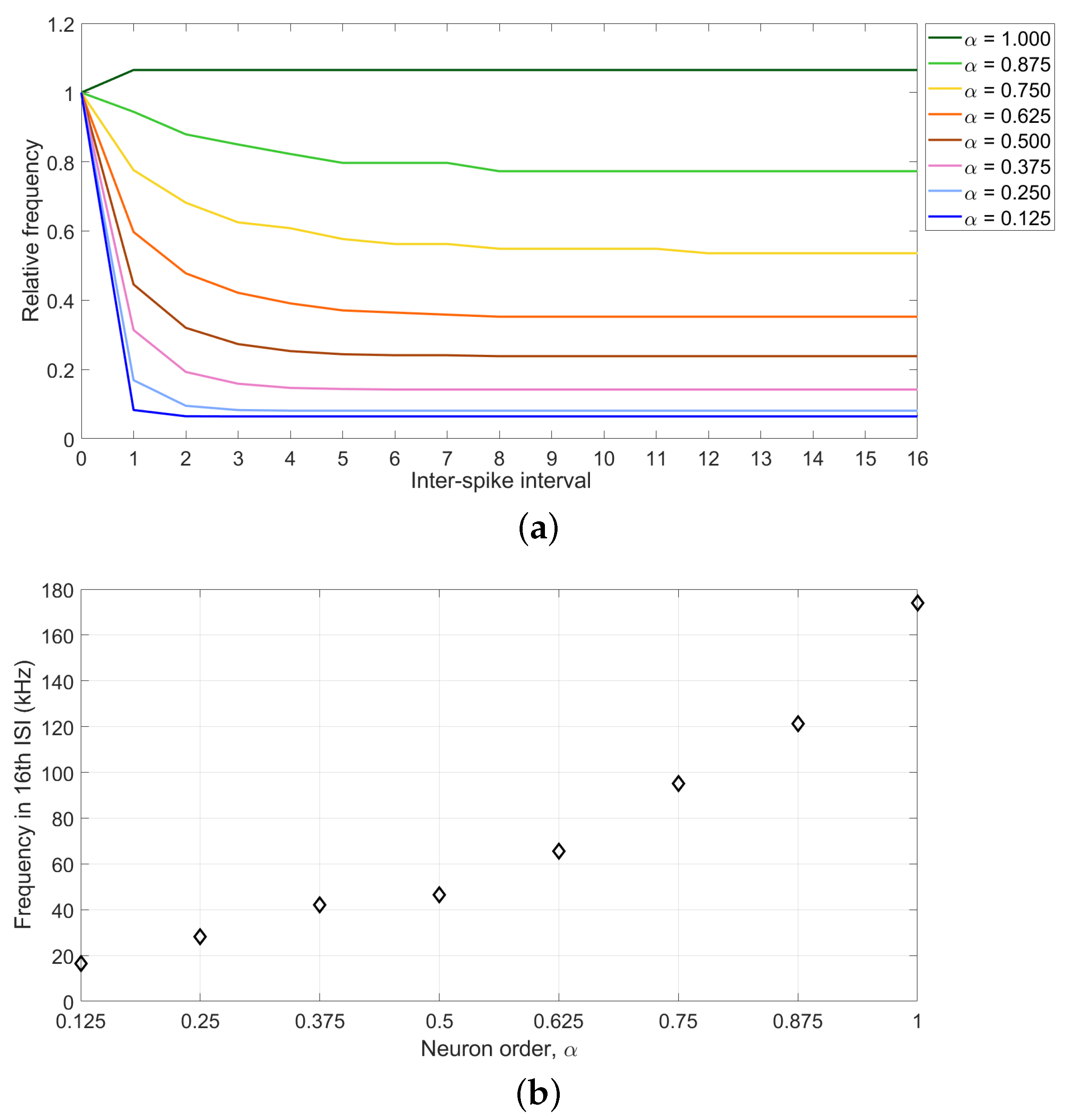
  • Two types of FO neurons were implemented based on integer-order neurons and FO derivatives connected at their inputs to search for behaviors inspired in real neurons. Specifically, the FO-DP and FO-TPFM neurons were created by combining the integer-order neurons, which can perform PFM, and the FO derivative using BFs in series. The results showed that both types of FO neurons are capable of adapting to inputs, i.e., evidenced the change in firing patterns observed when dealing with constant or periodic stimuli. The study evaluated two properties of adaptation based on theoretical analysis in the literature: (1) the increasing or decreasing spacing between spikes for a constant stimulus over time, and (2) the dependence of baseline frequency on FO. Here, an analog approach to obtain both properties simultaneously has been achieved, which was an open problem in the literature.
  • In this work, the key to obtain the FO version of the neurons was not to replace the components of their associated circuit with their analogous FO but rather to use their equivalent block diagram (shown in Figure 8a and Figure 12a for the DP and TPFM cases, respectively), which can be related to blocks in the FPAA. Note that, as reported in [26], the generalization of a capacitor to FO (i.e., the use of a fractional impedance) causes the loss of the adaptation properties of the FO neuron. In the context of traditional analog circuits (non-programmable), the proposed block diagram could be implemented by using an op-amp-based FO differentiator connected to the input of the integer-order neuron.

5. Conclusions

In this paper, the analog implementation of the Axon-Hillock (A-H) silicon neuron, with the functionalities available in a field-programmable analog array (FPAA) has been carried out. A new type of silicon neuron, the true-pulse-frequency modulation (TPFM) neuron, useful for modulation with appreciable pulse width, was also implemented. Only one FPAA was required for each neuron. In addition, the implementation of fractional-order (FO) neurons, which show adaptation like some biological neurons in response to constant or periodic stimulus, was accomplished.
Simulations were performed in the programming environment AnadigmDesigner2. The results obtained showed that the implemented neurons work correctly, which can be directly downloaded into a real FPAA.
The FPAA is convenient for prototyping when dealing with analog circuits, such as those of silicon neurons. Some limitations were found due to the switched capacitor technology used in the FPAA, like having sampled signals and quantized parameters.
Regarding future works, experimental tests have been planned to evaluate the neurons in real conditions. Also, its application to neuromorphic control (NC) will be tested.

Author Contributions

Conceptualization, I.T. and B.M.V.; methodology, A.J.S.-B., I.T., and B.M.V.; software, A.J.S.-B.; validation, A.J.S.-B.; formal analysis, A.J.S.-B.; investigation, A.J.S.-B.; resources, I.T. and B.M.V.; data curation, A.J.S.-B.; writing—original draft preparation, A.J.S.-B. and I.T.; writing—review and editing, A.J.S.-B., I.T., and B.M.V.; visualization, A.J.S.-B.; supervision, I.T. and B.M.V.; project administration, I.T. and B.M.V.; funding acquisition, I.T. and B.M.V. All authors have read and agreed to the published version of the manuscript.

Funding

This research was funded by the Agencia Estatal de Investigación (Ministerio de Ciencia e Innovación) through the projects PID2019-111278RB-C22/AEI/10.13039/501100011033 and PID2022-141409OB-C22/AEI/10.13039/501100011033/FEDER, UE and by the European Regional Development Fund (FEDER) “A way to make Europe”. Andrés Serrano would like to thank the Ministerio de Ciencia, Innovación y Universidades for its support through the scholarship no. FPU22/00885 of the FPU Program.

Data Availability Statement

Data are contained within the article.

Conflicts of Interest

The authors declare no conflicts of interest.

Abbreviations

The following abbreviations are used in this manuscript:
A-HAxon-Hillock
BFBilinear filter
CABConfigurable analog block
CAMConfigurable analog module
CHAnadigmDesigner2 oscilloscope channel
DPDirac delta-pulsed
FOFractional order
FO-DPFractional-order Dirac delta-pulsed
FO-I&FFractional order integrate and fire
FO-TPFMFractional-order true-pulse-frequency modulation
FPGAField-programmable gate array
FPAAField-programmable analog array
I&FIntegrate and fire
I/OInput/output
IPFMIntegral pulse-frequency modulation
ISIInter-spike interval
LUTLook-up table
NCNeuromorphic control
PFEPartial fraction expansion
PFMPulse-frequency modulation
SRMSpike response model
TPFMTrue-pulse-frequency modulation
VMRMid-rail voltage

Appendix A

The IPFM neuron model presented in this paper can be related to other neuron models through generalized models, such as the spike response model (SRM) [28], which is modeled using the following equation:
u ( t ) = f η ( t t f ) + 0 κ ( s ) I e x t ( t s ) d s + u r e s t
where u ( t ) is the membrane potential, I e x t is the stimulating current, κ describes the voltage response to the input, η is the spike after-potential function (i.e., how the potential changes after firing a pulse), u r e s t is the resting potential, and t f is the instant at which a spike is fired. Spike firing is defined by a threshold process. If the membrane potential reaches the threshold ϑ , an output spike is triggered at t = t f .
This model can be seen as a generalization of I&F models and includes phenomena of real neurons such as adaptation, refractoriness, and stochastic spiking by using the kernels [28].
Hence, it is possible to relate the SRM and IPFM by particularizing the SRM and combining Equations (3) and (4) of the IPFM in one equation as follows. First, let us assume a resting potential of zero ( u r e s t = 0 ) in the SRM, as is considered in the IPFM by Equation (4):
u ( t ) = f η ( t t f ) + 0 κ ( s ) I e x t ( t s ) d s
Second, if the after-potential function η is selected to behave as in (4) (when K t i is reached, the potential suddenly drops to 0), the first term of the SRM equation can be rewritten as:
f η ( t t f ) = f K t i δ ( t t f )
Third, the second term of the SRM equation can be interpreted as a convolution involving the kernel κ ( s ) and the incoming stimulus I e x t , i.e., as the linear response of the membrane potential to an input current or as the neuron responsiveness to incoming stimuli. If a unitary kernel (i.e., κ ( s ) = 1 ) is selected to imitate (3) (namely, the neuron responds equally to all incoming stimuli and they are not filtered), the SRM equation is simplified to:
u ( t ) = f K t i δ ( t t f ) + 0 I e x t ( t ) d t
Lastly, Equations (3) and (4) express the firing condition of the IPFM in terms of two successive pulses, i.e., what happens to the integrator output between t k 1 and t k , while the SRM equation describes the voltage curve from 0 to , with t f being the firing instants. We can express the integrator output of the IPFM in a similar way to the SRM by using an equation with two terms on the right side:
y ( t ) = k K t i δ ( t t k ) + 0 x ( t ) d t
Under these assumptions, it is noticeable that variables x ( t ) , y ( t ) , and t k in the IPFM have similar interpretations as variables I e x t ( t ) , u ( t ) , and t f from the SRM, respectively.
In summary, there exist many types of neuron models, but not all of them exhibit the behavior of the IPFM, which results in a firing frequency that is directly proportional to the input amplitude. Linear modulation is not properly achieved when the SRM uses other assumptions, such as different kernels, or when stochastic firing and refractoriness are introduced.

Appendix B

Because the signals in an FPAA are sampled and the simulations are based on difference equations, the solution may differ slightly from what would be expected in purely analog circuits. This appendix details the sampled dynamics of the proposed TPFM neuron.
The first integrator, acting as a DP neuron, does not fire impulses but a pulse with a duration equal to the inverse of the block frequency, in this case T s = 250 ns. This causes the second integrator to start with an initial condition equal to the area of this pulse times the integration constant of the input, i.e., V D D T s τ 2 , 1 C instead of V D D τ 2 , 1 C corresponding to the continuous case. In addition, the time in the high state, t h , depends on the difference equation that describes the behavior of the second integrator, which, according to the documentation, is given as follows:
y ( n ) = τ 2 , 2 C y ( n 1 ) Δ t + y ( n 1 )
where n represents discrete time. The solution of this equation is:
y ( n ) = c 1 ( 1 + τ 2 , 2 C T s ) n 1
with y ( 1 ) = V D D T s τ 2 , 1 C , where n = 1 was considered at the beginning of the pulse for simplification. Therefore, for the pulse to end, the following condition must be satisfied:
V D D T s τ 2 , 1 C ( 1 + τ 2 , 2 C T s ) n 1 U 2 C
which leads to the following number of simulation steps until the condition is satisfied:
n 1 + ln U 2 C V D D T s τ 2 , 1 C ln 1 + τ 2 , 2 C T s
Likewise, the actual value of t h is a multiple of T s , which can be obtained from the value of n as:
t h = n T s
In short, the following equation is used to adjust the threshold to obtain the desired t h :
U 2 C = V D D T s τ 2 , 1 C ( 1 + τ 2 , 2 C T s ) t h T s 1
where . denotes the ceiling operator. Alternatively, the gain can be tuned using:
τ 2 , 2 C = 1 T s U 2 C V D D T s τ 2 , 1 C t h T s 1 1 1
In this work, (A12) was used to adjust the value of the integrator gain, making U 2 C equal to V D D .

References

  1. Mead, C. Neuromorphic electronic systems. Proc. IEEE 1990, 78, 1629–1636. [Google Scholar] [CrossRef]
  2. Mead, C. Analog VLSI and Neural Systems; Addison Wesley: Boston, MA, USA, 1989. [Google Scholar]
  3. Marković, D.; Mizrahi, A.; Querlioz, D.; Grollier, J. Physics for neuromorphic computing. Nat. Rev. Phys. 2020, 2, 499–510. [Google Scholar] [CrossRef]
  4. Jones, R.W.; Li, C.C.; Meyer, A.U.; Pinter, R.B. Pulse Modulation in Physiological Systems, Phenomenological Aspects. IRE Trans. Bio-Med. Electron. 1961, 8, 59–67. [Google Scholar] [CrossRef] [PubMed]
  5. Liou, W.R.; Yeh, M.L.; Kuo, Y.L. A High Efficiency Dual-Mode Buck Converter IC For Portable Applications. IEEE Trans. Power Electron. 2008, 23, 667–677. [Google Scholar] [CrossRef]
  6. DeWeerth, S.; Nielsen, L.; Mead, C.; Astrom, K. A simple neuron servo. IEEE Trans. Neural Netw. 1991, 2, 248–251. [Google Scholar] [CrossRef] [PubMed]
  7. Indiveri, G.; Linares-Barranco, B.; Hamilton, T.; van Schaik, A.; Etienne-Cummings, R.; Delbruck, T.; Liu, S.C.; Dudek, P.; Häfliger, P.; Renaud, S.; et al. Neuromorphic Silicon Neuron Circuits. Front. Neurosci. 2011, 5, 73. [Google Scholar] [CrossRef] [PubMed]
  8. Teka, W.; Marinov, T.M.; Santamaria, F. Neuronal Spike Timing Adaptation Described with a Fractional Leaky Integrate-and-Fire Model. PLoS Comput. Biol. 2014, 10, e1003526. [Google Scholar] [CrossRef] [PubMed]
  9. Angkeaw, K.; Pongyart, W.; Prommee, P. Design and Implementation of FPAA based LQR Controller for Magnetic Levitation Control System. In Proceedings of the 2019 42nd International Conference on Telecommunications and Signal Processing (TSP), Budapest, Hungary, 1–3 July 2019; IEEE: Piscataway, NJ, USA, 2019. [Google Scholar] [CrossRef]
  10. Silva-Juarez, A.; Tlelo-Cuautle, E.; de la Fraga, L.G. Chapter Eight - FPAA-based implementation of fractional-order multidirectional multiscroll chaotic oscillators. In Fractional Order Systems; Radwan, A.G., Khanday, F.A., Said, L.A., Eds.; Emerging Methodologies and Applications in Modelling; Academic Press: Cambridge, MA, USA, 2022; Volume 1, pp. 341–374. [Google Scholar] [CrossRef]
  11. Altun, K. FPAA Implementations of Fractional-Order Chaotic Systems. J. Circuits Syst. Comput. 2021, 30, 2150271. [Google Scholar] [CrossRef]
  12. Silva-Juárez, A.; Tlelo-Cuautle, E.; de la Fraga, L.G.; Li, R. FPAA-based implementation of fractional-order chaotic oscillators using first-order active filter blocks. J. Adv. Res. 2020, 25, 77–85. [Google Scholar] [CrossRef] [PubMed]
  13. Hassanein, A.M.; Madian, A.H.; Radwan, A.G.G.; Said, L.A. On the Design Flow of the Fractional-Order Analog Filters Between FPAA Implementation and Circuit Realization. IEEE Access 2023, 11, 29199–29214. [Google Scholar] [CrossRef]
  14. Kapoulea, S.; Psychalinos, C.; Elwakil, A.S. FPAA-Based Realization of Filters with Fractional Laplace Operators of Different Orders. Fractal Fract. 2021, 5, 218. [Google Scholar] [CrossRef]
  15. Singh, N.; Mehta, U.; Kothari, K.; Cirrincione, M. Optimized fractional low and highpass filters of (1+α) order on FPAA. Bull. Pol. Acad. Sci. Tech. Sci. 2020, 68, 635–644. [Google Scholar] [CrossRef]
  16. Emad, S.; Hassanein, A.M.; AbdelAty, A.M.; Madian, A.H.; Radwan, A.G.; Said, L.A. A Study on Fractional Power-Law Applications and Approximations. Electronics 2024, 13, 591. [Google Scholar] [CrossRef]
  17. Pagidas, A.; Psychalinos, C.; Elwakil, A.S. Field Programmable Analog Array Based Non-Integer Filter Designs. Electronics 2023, 12, 3427. [Google Scholar] [CrossRef]
  18. Khanday, F.A.; Kant, N.A.; Dar, M.R.; Zulkifli, T.Z.A.; Psychalinos, C. Low-Voltage Low-Power Integrable CMOS Circuit Implementation of Integer- and Fractional–Order FitzHugh–Nagumo Neuron Model. IEEE Trans. Neural Netw. Learn. Syst. 2019, 30, 2108–2122. [Google Scholar] [CrossRef] [PubMed]
  19. Li, C.; Jones, R. Integral pulse frequency modulated control systems. IFAC Proc. Vol. 1963, 1, 186–195. [Google Scholar] [CrossRef]
  20. Abbott, L. Lapicque’s introduction of the integrate-and-fire model neuron (1907). Brain Res. Bull. 1999, 50, 303–304. [Google Scholar] [CrossRef] [PubMed]
  21. Valério, D.; Sá da Costa, J. An Introduction to Fractional Control; Institution of Engineering and Technology: Hong Kong, China, 2012. [Google Scholar] [CrossRef]
  22. Anadigm. AnadigmApex dpASP Family User Manual; Anadigm: Paso Robles, CA, USA, 2006. [Google Scholar]
  23. Caponetto, R.; Dongola, G.; Fortuna, L.; Petras, I. Fractional Order Systems: Modeling And Control Applications; World Scientific: Singapore, 2020. [Google Scholar] [CrossRef]
  24. Kapoulea, S.; Psychalinos, C.; Elwakil, A.S. Versatile Field-Programmable Analog Array Realizations of Power-Law Filters. Electronics 2022, 11, 692. [Google Scholar] [CrossRef]
  25. AbdelAty, A.; Fouda, M.; Eltawil, A. On numerical approximations of fractional-order spiking neuron models. Commun. Nonlinear Sci. Numer. Simul. 2022, 105, 106078. [Google Scholar] [CrossRef]
  26. Bertsias, P.; Psychalinos, C.; Elwakil, A.S. Fractional-Order Mihalas–Niebur Neuron Model Implementation Using Current-Mirrors. In Proceedings of the 2019 6th International Conference on Control, Decision and Information Technologies (CoDIT), Paris, France, 23–26 April 2019; pp. 872–875. [Google Scholar] [CrossRef]
  27. Serrano-Balbontín, A.J.; Tejado, I.; Vinagre, B.M. Fractional Integrate-and-Fire Neuron: Analog Realization and Application to Neuromorphic Control. In Proceedings of the 2023 International Conference on Fractional Differentiation and Its Applications (ICFDA), Ajman, United Arab Emirates, 14–16 March 2023; pp. 1–6. [Google Scholar] [CrossRef]
  28. Gerstner, W.; Kistler, W.M.; Naud, R.; Paninski, L. Neuronal Dynamics: From Single Neurons to Networks and Models of Cognition; Cambridge University Press: Cambridge, UK, 2014. [Google Scholar] [CrossRef]
Figure 1. Illustration of action potentials in biological neurons.
Fractalfract 08 00226 g001
Figure 2. Illustration of output pulses in PFM and some I&F neurons.
Fractalfract 08 00226 g002
Figure 3. Schematic of SS-IPFM.
Fractalfract 08 00226 g003
Figure 4. Illustration of (a) simple I&F neuron circuit and (b) A-H circuit. Adapted from [7].
Fractalfract 08 00226 g004
Figure 5. Evolution of the integral ( V B ( t ) ) in an A-H neuron.
Fractalfract 08 00226 g005
Figure 6. Architecture of an Anadigm® FPAA. Image extracted from user manual [22].
Fractalfract 08 00226 g006
Figure 7. Resistance as switched capacitor and non-overlapping phases.
Fractalfract 08 00226 g007
Figure 8. DP neuron: (a) block diagram and (b) evolution of the integrator output.
Fractalfract 08 00226 g008
Figure 9. Schematic implemented in AnadigmDesigner2 to reproduce the DP neuron.
Fractalfract 08 00226 g009
Figure 10. A-H-like neuron: (a) block diagram and (b) evolution of the two integrator outputs.
Fractalfract 08 00226 g010
Figure 11. Schematic implemented in AnadigmDesigner2 to reproduce the A-H neuron.
Fractalfract 08 00226 g011
Figure 12. TPFM neuron: (a) block diagram and (b) evolution of the two integrators outputs.
Fractalfract 08 00226 g012
Figure 13. Schematic implemented in AnadigmDesigner2 to reproduce the true-PFM neuron.
Fractalfract 08 00226 g013
Figure 14. Schematic implemented in AnadigmDesigner2 to reproduce a third-order approximation of the FO operator using: (a) CAMs as zero-pole pairs in series, (b) CAMs as low-pass filters, and (c) integrators and gains.
Fractalfract 08 00226 g014
Figure 15. Block diagram of: (a) FO-DP neuron and (b) FO-TPFM neuron.
Fractalfract 08 00226 g015
Figure 16. Schematic implemented in AnadigmDesigner2 to reproduce: (a) FO-DP neuron using BFs in series and (b) FO-TPFM neuron using BFs in series.
Fractalfract 08 00226 g016
Figure 17. Simulation results for integer-order neurons in AnadigmDesigner2: (a) DP neuron, (b) A-H neuron, and (c) TPFM neuron.
Fractalfract 08 00226 g017
Figure 18. Simulation results for the FO operator of order 0.5 in AnadigmDesigner2: (a) input, integer derivative (s), and FO derivative using BFs in series and (b) FO derivative using BFs in series, BFs in parallel, and using individual integrators.
Fractalfract 08 00226 g018
Figure 19. Simulation results for FO-DP neuron in AnadigmDesigner2: (a) input, FO derivative, integration and fired pulses for α = 0.5 and (b) output pulses for α 1 = 1 , α 2 = 0.75 , α 3 = 0.5 , and α 4 = 0.25 .
Fractalfract 08 00226 g019
Figure 20. Simulation results for FO-TPFM neuron in AnadigmDesigner2: (a) input, FO derivative, integration, and fired pulses for α = 0.5 and (b) output pulses for α 1 = 1 , α 2 = 0.75 , α 3 = 0.5 , and α 4 = 0.25 .
Fractalfract 08 00226 g020
Figure 21. Simulation results corresponding to FO-TPFM neuron when changing the neuron order α : (a) normalized pulse frequency and (b) last frequency dependence.
Fractalfract 08 00226 g021
Table 1. Comparison of integer-order neuron implementations.
CharacteristicDP NeuronA-H NeuronTPFM Neuron
Pulse widthNon-tunable
t h A = 1 f s
Tunable
t h B = U 2 B τ 2 B V D D
Tunable
t h C = 1 τ 2 , 2 C ln U 2 C τ 2 , 1 C V D D
Firing frequencyLinear
f A = τ 1 A i ¯ U 1 A
Nonlinear
f B = U 3 B τ 1 B i ¯ + U 2 B τ 2 B V D D 1
Linear
f C = τ 1 C i ¯ U 1 C
CAM neededIntegrator with
comparator
Two Integrators with
comparators
Comparator
Inverting Sum Stage
DC Voltage Source
Inverting Gain Stage
Integrator and Sum Integrator
with comparators
Comparator
Inverting Sum Stage
DC Voltage Source
Inverting Gain Stage
Power consumption
(software estimation)
40 mW94 mW96 mW
Table 2. Parameters used in the three types of implementations for s 0.5 .
BFs in SeriesBFs in ParallelIndividual Integrators
Approximation f b = 2 kHz f b = 63.66 Hz
( N = 3 ) f h = 400 kHz f h = 400 kHz
Implementation f p 1 = 7.52 kHz f 0 1 = 7.52 kHz τ 1 = 0.532 µs−1
f p 2 = 43.98 kHz f 0 2 = 43.98 kHz τ 2 = 0.147 µs−1
f p 3 = 257.22 kHz f 0 3 = 257.22 kHz τ 3 = 1.570 µs−1
f z 1 = 3.11 kHz G 1 = 0.26 τ 4 = 1.710 µs−1
f z 2 = 18.19 kHz G 2 = 0.72 τ 5 = 0.055 µs−1
f z 3 = 106.37 kHz G 3 = 2.52 τ 6 = 0.203 µs−1
G C 0 = 3.76 G c 0 = 3.76 G c 0 = 5.00
G H F 1 = 1.00 G 1 = 1.00
G H F 2 = 1.00 G 2 = 0.01
G H F 3 = 1.00 G 3 = 0.01
G S = 0.24
Disclaimer/Publisher’s Note: The statements, opinions and data contained in all publications are solely those of the individual author(s) and contributor(s) and not of MDPI and/or the editor(s). MDPI and/or the editor(s) disclaim responsibility for any injury to people or property resulting from any ideas, methods, instructions or products referred to in the content.

