Abstract
The implementation of additive manufacturing technology (e.g., digital printing) to the electronic packaging segment has recently received increasing attention. In almost all types of Fan-out wafer level packaging (FOWLP), redistribution layers (RDLs) are formed by a combination of photolithography, sputtering and plating process. Alternatively, in this study, inkjet-printed RDLs were introduced for FOWLP. In contrast to a subtractive method (e.g., photolithography), additive manufacturing techniques allow depositing the material only where it is desired. In the current study, RDL structures for different embedded modules were realized by inkjet printing and further characterized by electrical examinations. It was proposed that a digital printing process can be a more efficient and lower-cost solution especially for rapid prototyping of RDLs, since several production steps will be skipped, less material will be wasted and the supply chain will be shortened.
1. Introduction
FOWLP is a rapidly growing high-density packaging technology, which has many advantages such as short interconnection, low thermal resistance, high RF performance, and small package outline dimension. A lot of activities are running worldwide dealing with FOWLP. It can be used for multi-chip packages for System in Package (SiP) and heterogeneous integration. However, there are still several technical challenges facing FOWLP that need to be overcome, such as the die shifting issue, warpage due to the material coefficient of thermal expansion (CTE) mismatch and the fabrication cost and complexity of the redistribution layers (RDL). For FOWLP two basic process flows are encountered: the “mold-first” or the “RDL first” approach [1,2,3]. The mold-first process flow is depicted in Figure 1, beginning with the placement of known-good-dies onto a temporary carrier with thermal release tape laminated on top. After overmolding and subsequent release of the temporary adhesive tape, the redistribution layers (RDL) are fabricated (step 5). RDLs are typically metal interconnection schemes or metal traces that route the electrical signals from one part of the package to another. This is usually achieved by combining photolithographic processes, as well as sputtering and plating. In the case of a high-density FOWLP, multiple layers of RDL are required to support the necessary routing. The metal traces together with dielectric isolation layers generate multi-layer RDLs.
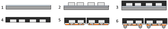
Figure 1.
The process flow of mold-first FOWLP; (1) thermal release tape laminated on top of the temporary carrier, (2) face-down die-attach of the known-good-dies, (3) overmolding, (4) carrier removal, (5) RDL fabrication and (6) balling & dicing.
In the present study, however, an alternative approach is investigated, namely inkjet printing of metallic routes, thereby allowing for fast prototyping, which typically is not possible with RDL formation via multiple process steps. In another article, screen-printed Ag paste was suggested as to realize RDL structures and fill the vias [4].
2. Materials and Methods
2.1. Methodology
A wafer-level SiP concept was pursued in this project, in which capacitive MEMS microphones together with their respective low power ASICs are molded simultaneously in a single package. As schematically shown in Figure 2, in order to connect the microphones pads to the ASICs as well to fan out the signals via solder balls, RDL structures are required. As seen, the main benefit of using inkjet printing for fabricating RDLS instead of photolithography is the shortened supply chain, by which rapid prototyping of such customized SiPs would be much easier. Another benefit of inkjet printing also comes from its digital or on-demand deposition capability [5]. The whole procedure of photoresist coating, baking, exposure, development, seed layer sputtering, metal plating and etching can be replaced by inkjet printing of single or multilayers of metallic and dielectric inks followed by sintering. In our previous works, inkjet printed Ag traces were introduced as a versatile means for rapid prototyping of electronic packages [6,7].
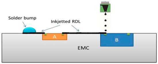
Figure 2.
Schematic demonstration of inkjet-printed RDLs for a SiP FOWLP.
2.2. Materials
In this study 8 (200 mm) wafers are fabricated using an epoxy molding compound with spherical SiO2 filler particles with a size of max. 75 µm. Inkjet printing of Ag tracks was carried out by employing an advanced R&D inkjet printer with a 50 μm nozzle diameter and 50 pl calibrated drop size. A commercial nanoparticle Ag ink with 50 wt% metal loading and average particle size of 110 nm (d90) was deposited at the operational jetting voltage of 100 V, printing frequency of 500 Hz and at carefully adjusted jetting pulse duration profile. The printing was performed at room temperature, while the substrate was heated-up to 50 °C. The most efficient sintering methodology for the printed Ag RDLs (e.g., pulsed light sintering, thermal sintering, plasma sintering etc.) was subsequently determined by means of the four-point probe measurements [8]. In fact, since different materials with divergent surficial and physical properties are found in SiP, which are exposed to the light or plasma source concurrently, the uniform treatment of the inkjet printed Ag nanoparticles was not effective. On the contrary, upon thermal curing at 150 °C for 1 h, Ag lines were sintered uniformly regardless of the material beneath. Considering the printing head’s configuration used in this study and Ag/ EMC’s surficial properties, the minimum width and pitch size of the Ag tracks was defined to be 80 µm and 160 µm respectively. The pads on the chip were 100 µm in diameter.
The morphology of the printed RDLs was characterized using scanning electron microscopy (SEM, Quanta 200 FEGSEM, FEI) and focused ion beam work station (FIB, Quanta 200 3D, FEI). A Pt-based thin layer was deposited onto the surface in order to protect the surface of printed traces from incurring FIB induced damage.
3. Results and Discussion
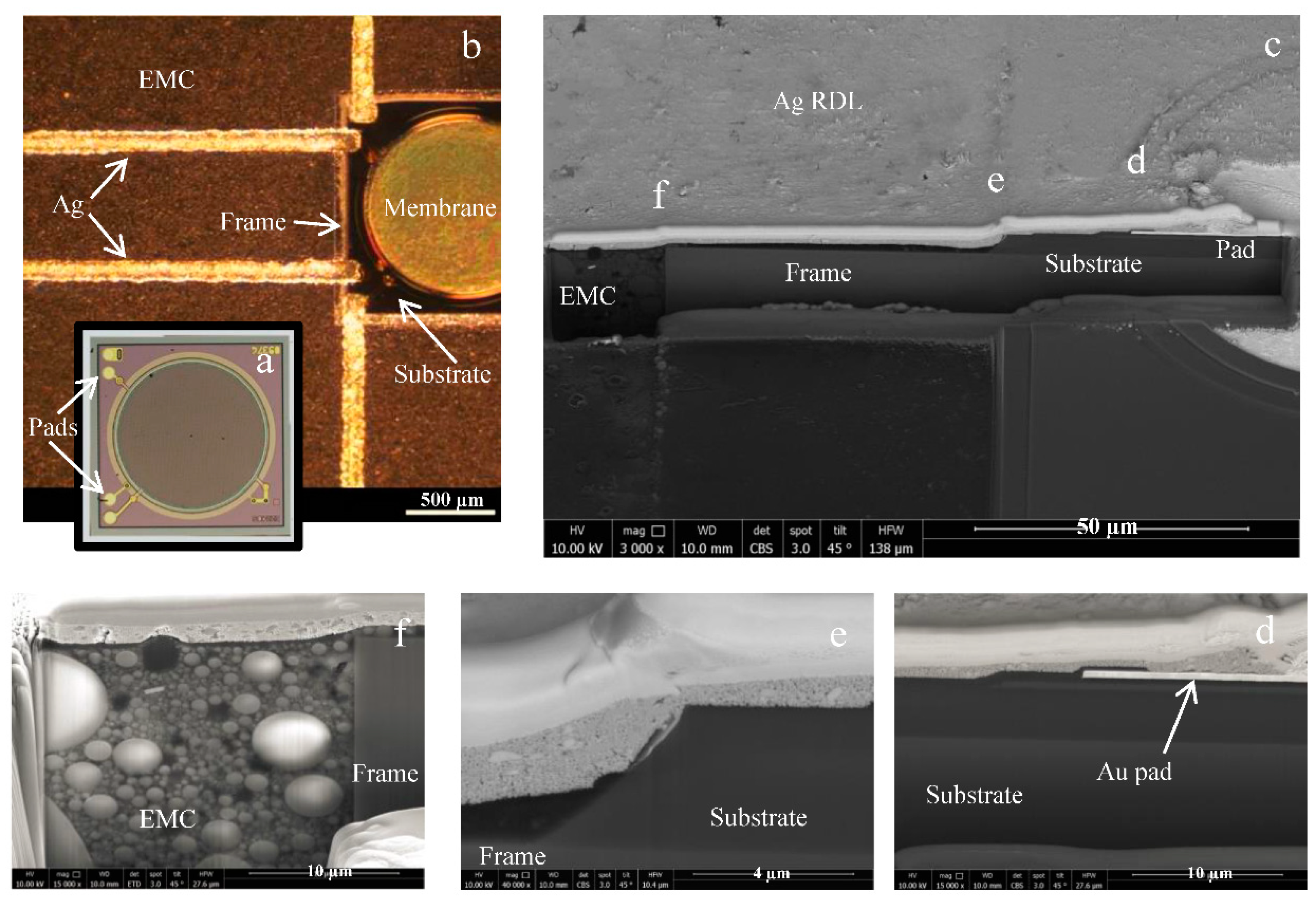
In Figure 3, one realization of the inkjet printed RDLs for FOWLP is demonstrated. The respective cross-sectional image is shown in Figure 3c–f. As seen, 4 Ag lines resembling single-layer RDL structure were generated as to connect the Au-pads of the chip to other components. As inferred from these figures, Ag lines managed to cross over four levels; chip pad, substrate, frame and mold. The corresponding interfaces, spotlighted in Figure 3, are Au-pad to SiO2 substrate (3 c), SiO2 substrate to the chip frame (3 d) and the frame to EMC mold (3 e). As inferred from these figures, sharp steps can be considered as the bottleneck for printed line. While the molded components should principally stay flat at the wafer level, depending on the material selection and process conditions, the components might encounter few micrometer out-of-plane offset. Given that, it was observed that the molded components were 3–6 µm higher than the mold wafer’s surface.

Figure 3.
An example for inkjet-printed RDLs in FOWLP; a microphone chip with 4 pads before molding. (a) and a molded one with Ag RDLs (b); the corresponding FIB-cut cross-sectional view (c) and the three critical interfaces between pad-substrate (d), substrate-frame (e) and frame-mold (f).
The functionality of the Ag traces, in terms of electrical conductivity was successively assessed which is given in Table 1. The configurations of the inkjet printed Ag RDLs were compared to those of conventional RDLs fabricated by photolithography and plating. As perceived from this list, some fundamental differences in the final properties of the RDLs can be recognized. Suffice to say, that inkjet-printed RDLs are required to be adjusted with respect to the respective substrate materials. Due to the temperature restrictions of the EMC, thermal sintering of the Ag lines were applicable only up to 150 °C. It was found that thermal sintering at higher temperatures (>150 °C) lead to an increase of wafer warpage, most likely caused by the proceeding cure reaction of the molding compound and the resulting cure shrinkage. The thickness of the inkjetted RDLs can be simply increased by multi-pass printing, whereas the multilayered RDLs were feasible by a successive printing of alternate layers of Ag and dielectric structures.

Table 1.
Material properties of the inkjet printed RDLs in comparison to the conventional RDLs.
4. Conclusions
In this study, the feasibility of employing inkjet printing in FOWLP was investigated. It was shown that inkjet printed Ag lines can be a promising alternative to conventional RDLs produced by photolithography and electroplating. Different sintering techniques were assessed, where thermal sintering appeared to be the most suitable methodology. Though thermal curing can cause increased mold wafer warpage, that can be nevertheless handled during the process flow until package singulation. It was revealed that small out-of-plane offsets of the molded compounds can be tolerated and functional RDL structures can be generated.
Acknowledgments
This work was carried out within the framework of the project “SILENSE”, co-financed by the European Union’s HORIZON 2020 program.
Conflicts of Interest
The authors declare no conflict of interest.
References
- Braun, T.; Becker, K.F. Trends in Fan-out wafer and panel level packaging. In Proceedings of the 2017 International Conference on Electronics Packaging (ICEP), Yamagata, Japan, 19–22 April 2017; pp. 325–327. [Google Scholar] [CrossRef]
- Lujan, A.P. A cost analysis of RDL-first and mold-first fan-out wafer level packaging. In Proceedings of the 2016 International Conference on Electronics Packaging (ICEP), Sapporo, Japan, 20–22 April 2016; pp. 237–242. [Google Scholar] [CrossRef]
- Braun, T.; Kahle, R. Fan-Out Wafer and Panel Level Technology for Advanced LED Packaging. IWLPC Conference Proceedings. 2017. Available online: www.smta.org/knowledge/proceedings_abstract.cfm?PROC_ID=5118 (accessed on 24 October 2018).
- Chia-Yen, L.; Tsai, H. Printing Method for Redistribution Layer and Filling of through Silicon Vias Using Sintering Silver Paste. In Proceedings of the 2014 9th International Microsystems, Packaging, Assembly and Circuits Technology Conference (IMPACT), Taipei, Taiwan,, 22–24 October 2014. [Google Scholar] [CrossRef]
- Chen, S.P.; Chiu, H.L.; Wang, P.H. Inkjet printed conductive tracks for printed electronics. ECS J. Solid State Sci. Technol. 2015, 4, P3026–P3033. [Google Scholar] [CrossRef]
- Krivec, M.; Roshanghias, A.; Binder, A. 3DInkPack—Inkjet Printing of Discrete Sensor Packages for Advanced Rapid Prototyping. Proceedings 2017, 1, 609. [Google Scholar] [CrossRef]
- Roshanghias, A.; Krivec, M.; Bardong, J. Printed SAW transponder package for rapid prototyping of electronic packages. In Proceedings of the 2016 6th Electronic System-Integration Technology Conference (ESTC), Grenoble, France, 13–15 September 2016. [Google Scholar] [CrossRef]
- Roshanghias, A.; Krivec, M.; Baumgart, M. Sintering strategies for inkjet printed metallic traces in 3D printed electronics. Flex. Print. Electron. 2017, 2, 045002. [Google Scholar] [CrossRef]

Publisher’s Note: MDPI stays neutral with regard to jurisdictional claims in published maps and institutional affiliations. |
© 2018 by the authors. Licensee MDPI, Basel, Switzerland. This article is an open access article distributed under the terms and conditions of the Creative Commons Attribution (CC BY) license (https://creativecommons.org/licenses/by/4.0/).