A Generic Control-Oriented Model Order Reduction Approach for High Step-Up DC/DC Converters Based on Voltage Multiplier


1
College of Electrical Engineering & New Energy, China Three Gorges University, Yichang 443002, Hubei, China
2
School of Electrical Engineering and Computer Science, Queensland University of Technology, Brisbane, QLD 4001, Australia
3
School of Automation, Wuhan University of Technology, Wuhan 430070, Hubei, China
*
Author to whom correspondence should be addressed.
Energies 2019, 12(10), 1971; https://doi.org/10.3390/en12101971
Submission received: 10 April 2019
/
Revised: 15 May 2019
/
Accepted: 20 May 2019
/
Published: 23 May 2019
(This article belongs to the Special Issue Control in Power Electronics)
Abstract
:The modeling and control system design of high step-up DC/DC converters based on voltage multipliers (VMs) are difficult, due to the various circuit topologies and the presence of large number of capacitors in VMs. This paper proposes a generic approach to reduce the model order of such converters by replacing the VM capacitors with voltage sources controlled by the output voltage of the converter. Theoretical analysis and simulation results show that the derived models can accurately represent the low frequency response of the converter which is valuable for obtaining a small-signal AC model for control system design. The detailed modeling and controller design process are demonstrated for the converter, and the obtained simulation results are verified experimentally on a 400 W prototype.
1. Introduction
The desire for clean environment, low carbon emission and the fact that fossil fuel reserves are depleting have led to the rapid development of renewable energy generation systems. Renewable energy generating units, such as photovoltaic arrays and wind turbine generators, present lower output voltage compared to the interconnected grid systems, and thus high voltage step-up methods are required for grid integration. It is also important to provide active control to these energy conversion devices in order to maximize the energy harvested, which calls for high-efficiency power electronic converters. High step-up voltage conversion technology based on voltage multiplier (VM) is one of the solutions [1] and has recently become increasingly popular in renewable applications such as solar photovoltaic [2,3], wind power generation [4], and fuel cell power generation [5,6].
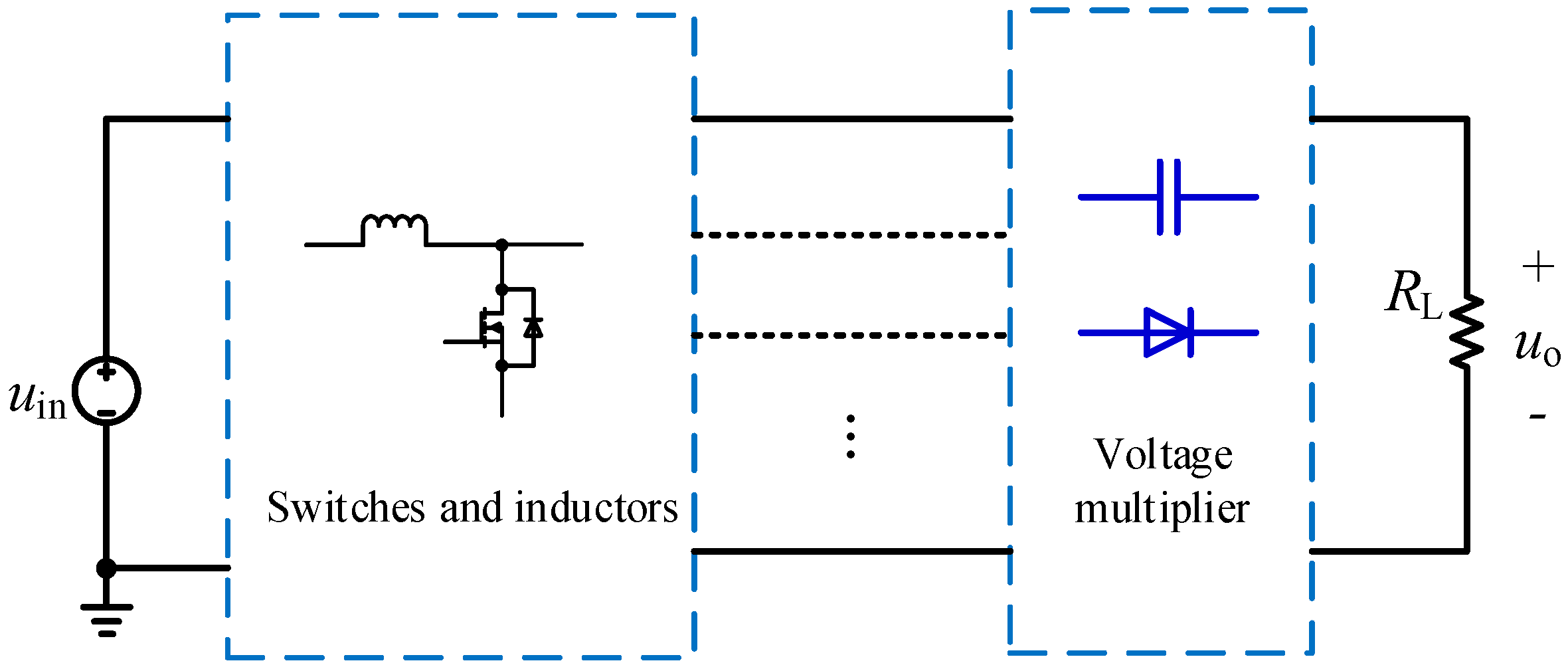
In recent years, various VM circuits have been proposed to achieve a family of high step-up non-isolated DC/DC converter topologies for the applications in renewables [7,8,9,10,11,12,13,14,15,16,17,18,19,20,21,22]. A generalized circuit structure of a family of non-isolated converters with VM is shown in Figure 1, where the switch/inductor circuit is connected to the diode-capacitor VM to supply the load RL. The output voltage uo of the converter can be stepped up to much higher level compared to the input voltage uin. For the diode-capacitor VM circuit, voltage doubler circuit [7], voltage quadrupler circuit [8], Dickson charge pump [9], Cockcroft–Walton VM [10], and amongst others [17] have been used, and based on which various other different VM circuits have been proposed for two-input-phase interleaved booster converter [5,11,12,13] and multiple-input-phase booster converter [4,14,15,16,19]. Coupled-inductor has been used to replace the inductors to provide further performance improvement [6,23,24].
However, most of the existing literature on this type of converter focus on derivation of the circuit topology and/or design optimization, while the determination of the control structure and the tuning of the control parameters are simply based on empirical methods, or even not discussed. The lack of systematic approach to modeling and control system design will lead to cumbersome parameter tuning process and/or poor performance of the converter, especially under highly-varying conditions of the renewable generations, which can offset the benefits of this type of promising converter. A large number of capacitors are used in VM circuits, which can effectively increase the voltage conversion gain and reduce the voltage stress of the switching devices, but this also leads to a high-order system and makes the classical model-based design of high-performance control system difficult, unless a suitable control-oriented model order reduction approach is developed for practical applications.
Indeed, modeling and model order reduction approaches have been developed for many VM-based converters, such as those with three-state switching cell [25], switch capacitor [26], coupled-inductor [27]. However, the existing approaches are specifically designed for relatively low-order system and they cannot be readily applied to other topologies, especially when the number of VM cells increases. To reduce the effort of control system design for a family of high step-up DC/DC converters based on diode-capacitor VM, for the first time, this paper proposes a novel general method to acquire their averaged-value reduced-order models. The approach uses the concept to replace all the capacitors in the VM with voltage sources controlled by the output voltage of the converter, and the system order is greatly reduced without sacrificing much model accuracy.
The rest of the paper is organized as follows: Detailed procedure of the proposed model-order reduction method is presented in Section 2. Using this proposed method, general small-signal AC models and relevant transfer functions for the converters based on VM are derived in Section 3. Controller design is included in Section 4, where the low frequency response of the proposed reduced-order small signal AC model is found to be in agreement with the simulation results from the circuit model with detailed switching dynamics. The proposed control design method based on the reduced-order model is verified through simulation and experiment in Section 5. The main findings of the work are concluded in Section 6.
2. Proposed Modeling Method and Reduced-Order Models
2.1. Proposed Model Order Reduction Method
For the type of converters as shown in Figure 1, it has been commonly found that by neglecting the effects of ripples, the voltage across each VM capacitor is in linear relationship to the output voltage uo of the converter [7,8,9,10,11,12,13,14,15,16,17,18,19,20,21,22]. Hence, each VM capacitor can be replaced by a controlled voltage source associated with uo. As the system order is determined by the number of the energy storage components in the circuit, the corresponding model order can be greatly reduced. Detailed procedure for the proposed model order reduction approach is described as follows:
- Step 1:
- Obtain the steady-state relationship between all VM capacitor voltages and the output voltage uo(t) according to the results from circuit analysis. The general relationship can be expressed aswhere ucn(t) is the voltage of n-th VM capacitor and kn is corresponding proportional gain.
- Step 2:
- Replace all VM capacitors, except the ones at the output, with controlled voltage sources according to (1). This step is shown graphically in Figure 2.
- Step 3:
- Reformulate and simplify the resulting model to construct an equivalent reduced-order circuit based on the state-space averaging method [28].
In this connection, the converter proposed in [12] will be used as an example to demonstrate the proposed approach. Figure 3a shows the topology of this converter with n number of basic VM cells. It consists of two switches S1 and S2, two inductors L1 and L2, and the VM circuits with n VMs. Each VM consists of two diodes and two capacitors with the equal capacitance Cia = Cib = Cik (i = 1, 2, …, n). The voltage conversion gain is 2n times of the traditional boost converter. The driving signals of switches S1 and S2 are interleaved and both duty cycles d shall be larger than 0.5. The conversion gain of this converter can be easily adjusted by changing the number of VMs at the design stage. Voltage stress of all semiconductor devices are reduced significantly compared with conventional boost converter, and the two inductor currents can be automatically self-balancing. All capacitors have the same current stress, except the two which are connected with the load, that is, conducive to the thermal design. We denote this converter as the VM converter hereafter in this paper.
The steady-state relationships between the capacitor voltage in VMs and the output voltage are given in (2) based on the analytical results provided in Reference [12]. According to Step 2 of the proposed model order reduction method, the equivalent circuit of this converter by replacing all capacitors in VMs with corresponding controlled voltage sources is shown in Figure 3b.
According to the working state of the switches, the operation mode of this converter can be separated into three regions during one switching period TS and the equivalent circuits for each region are shown in Figure 4.
Equation (3) can be obtained while S1 and S2 are both in on-state. Similarly, (4) is obtained when S1 is in on-state and S2 is in off-state. When S2 is turned-on and S1 is turned-off, (5) can be obtained.
Furthermore, according to Reference [12], when the duty cycles of S1 and S2 are identical, the average inductor currents of L1 and L2 over one switch period Ts shall be equal, i.e.,
Next, by replacing the state variables with their low-frequency averaged values over one switch period Ts, (3)–(6) can be simplified to
where d′ = 1 − d. Combining (2) and (7) yields the new governing equation of state of the capacitors, i.e.,
where 1≤ i ≤ n − 1.
Hence, the reduced-order model for the VM converter is obtained as (7) and (8). Based on (7) and (8), its equivalent circuit can be obtained as shown in Figure 5a. It can be clearly seen that the voltage is stepped up through n stages by using n ideal transformers. In the first stage the voltage increases by a factor of 2/d′(t), and later the voltage increases linearly. Indeed, by combining the inductors, the capacitors and the ideal transformers respectively, Figure 5a can be readily simplified to Figure 5b, where the equivalent parameters A and Leq can be readily obtained as
Considering that Cia = Cib = Cik, the equivalent capacitance Ceq,i of the i-th stage in Figure 5a referring to the final (n-th) stage is
If C1k = C2k = … Cnk = Ck, and considering, Equation (11) can be further reduced to
2.2. A General Reduced-Order Model of the Converters Based on VM
Using the similar method presented in Section 2.1, the reduced-order averaged models of the existing VM-based converters proposed in References, [9,10,11,14,16], are investigated and derived. It was found that all the reduced-order models share an identical equivalent circuit structure, as shown in Figure 5b, while the corresponding expressions for parameters Leq, Ceqo and A are different; they are summarized in Table 1.
3. Small Signal AC Models and Transfer Functions
3.1. Small-Signal AC Models
Based on the state-space averaging method and the proposed reduced-order averaged model as shown in Figure 5, the small-signal AC model of the VM converter can be obtained as
where Iin, Uo and D′ are the quiescent values of the input current iin(t), output voltage uo(t), and d′(t), respectively. , , and are the small AC values of the input current iin(t), output voltage uo(t), input voltage uin(t), and d′(t), respectively.
3.2. Transfer Functions
Based on Figure 6, the general transfer functions related to the controller or filter design of the converters based on VM are derived and given in (13)–(17), where A, B and C for different converter circuits are listed in Table 2.
(1) Control-output voltage transfer function
(2) Line-to-output voltage transfer function
(3) Control-input current transfer function
(4) Output impedance
(5) Input impedance
3.3. Accuracy of the Small Signal AC Model
To verify the accuracy and examine the performance of the proposed general small signal AC models and relevant transfer functions of the converters based on VM, a comparison between the proposed models and practical circuits, and controller design of the VM converter, will be presented in this section. The specifications for the simulation are listed in Table 3 and Table 4.
The simulation results are shown in Figure 7, Figure 8 and Figure 9, where the VM numbers are 2, 3, and 5, respectively. The blue line is the actual circuit simulation result using PSIM software, and the red line is the proposed model simulation result obtained from MATLAB R2016a/Simulink 8.7 (The MathWorks, Inc., Natick, MA, USA). When the VM number is 2, Figure 7a,c,e show the output voltage waveforms when the duty cycle changes around 0.6 with different voltage ripple on capacitors in VM due to different Cna and Cnb. Figure 7b,d,f show the output voltage waveforms when the input voltage changes around 40 V with different voltage ripple on capacitors in VM due to different Cna and Cnb. It can be seen from Figure 7 that the increase of voltage ripple on capacitor in VM will make the steady-state accuracy of the proposed model worse, but the dynamic response of the proposed model is not affected significantly. When the voltage ripple on capacitors in VM is 10%, Figure 7c, Figure 8a and Figure 9a show the output voltage waveforms when the duty cycle changes around 0.6 with different VM number at Cna = Cnb = 2 μF, while Figure 7d, Figure 8b and Figure 9b show the output voltage waveforms when the input voltage changes around 40 V with different VM number at the same capacitance. Clearly, as the VM number increases, the steady-state error between the proposed model and the actual circuit increases too. This steady-state error is causes by the ripple in the capacitor voltage which affects the converter voltage gain [12].
From the above observation, it can be seen that the proposed model will become less accurate in steady-state as the capacitor voltage ripple in VM or the number of VM cells increases. Nevertheless, these negative effects are very limited and negligible for control system design, which can be observed from Figure 7, Figure 8 and Figure 9. On the other hand, the proposed reduced-order model is capable of capturing the major dynamic characteristics of the detailed circuit model. This can be seen from Figure 7, Figure 8 and Figure 9, as the dynamic responses are very close. Above characteristics of the proposed reduced order model make it valuable in the controller design of the converter.
4. Controller Design
A voltage and current double-loop control scheme is designed and shown in Figure 10, where Gv(s) and Gi(s) are the transfer functions of the voltage and current regulators respectively. One/VM is the equivalent gain of the PWM modulator and it is equal to 1.33 V based on the control chip (ISL6558) specifications. Furthermore, H1(s) and H2(s) are the voltage and current measurement gain respectively. The system output voltage is 400 V, and its reference voltage uref is set to 4.0 V, so the voltage sampling factor H1(s) is kept at 0.01. The current measurement gain H2(s) is kept at 0.1.
The voltage loop gain is affected by the current loop gain, so the design of the current loop compensator needs to be completed first. The current loop gain without the current loop compensator Gi(s) can be obtained by (18) as Ti-e(s).
Based on Table 3 and (18) and the above parameters of VM and H2(s), Gid(s) and Ti-e(s) can be obtained as follows.
The current loop compensator Gi(s) with crossover frequency at 4.7 kHz, are designed as in (21). The Bode diagram for current loop gains with and without compensation are shown in Figure 11.
The voltage loop gain without the voltage loop compensator Gv(s) can be obtained by (22) as Tv-e(s).
Based on Table 3, (9)–(11), (13), and VM, H1(s) and H2(s), transfer functions Gud(s) and Tv-e(s) can be derived as follows.
The voltage loop compensator Gv(s) with crossover frequency at 513 Hz, are designed as in (25). The Bode diagrams for voltage loop gains with and without compensation are shown in Figure 12.
Furthermore, in order to validate the derived transfer functions (13) and (15) in frequency domain, Bode diagrams for Gid(s) and Gud(s) are obtained using both the derived small-signal AC model transfer functions using MATLAB/Simulink, and the computer simulations based on PSIM circuit, as shown in Figure 13. Apparently, the frequency response of the transfer functions from the proposed reduced-order model are in close agreement with the PSIM simulation results within the frequency range below 3 kHz, which means the proposed reduced-order model and the transfer functions can be used in the controller design.
5. Simulation and Experimental Verification
This section examines the performance of the controller designed using the method presented in Section 4. The simulation circuit shown in Figure 10a is implemented in PSIM and the simulation results are shown in Figure 14. The specifications of the simulation is given in Table 3 as the rated parameters. Figure 14a shows the response of the output voltage uo to step changes in the input voltage uin. The input voltage uin increases from 30 V to 40 V, and then drops back to 30 V in 50 ms. Figure 14b shows the simulation waveforms of the output voltage uo and the output current io for step changes in load resistance. The load resistance increases from 400 Ω to 800 Ω first, and then reduces to 400 Ω in 50 ms. Clearly, when uin changes suddenly, uo is capable of tracking its reference at a constant value, although a small overshoot about 18 V is observed during the transient. When the load resistance suddenly changes, uo can also follow its reference with a small overshoot of 28 V. It is worth noting that the output voltage will be rapidly re-stabilized to 400 V.
In order to further verify the efficacy of the proposed model, experimental prototype was set up as shown in Figure 15. The specifications of the experimental prototype are consistent with the rated parameters of the simulation model, as shown in Table 3.
Two scenarios are tested and the experimental results are compared with the simulated results.
First, the input voltage uin increases from 30 V to 40 V and then drops back to 30 V, and the voltage changes are limited by a maximum ramp rate of ±1 V/ms. The second scenario is similar to that for Figure 14b: the load increases suddenly from 400 Ω to 800 Ω and then drops back to 400 Ω. The experimental waveforms of the circuit variables are shown in Figure 16. It can be clearly observed that in both scenarios, the output voltages are well-regulated at the set-point. The overshoot of the output voltage is much smaller than that which is obtained from the simulation shown in Figure 14; such differences are caused by the limitation of the maximum change rate of the of the DC source and the load.
6. Conclusions
This paper proposes a method to develop control-oriented reduced-order models for a family of high step-up DC/DC converters based on VM with diode-capacitor network. It was found that a general reduced-order averaged model can be derived by replacing the VM capacitors with output-voltage-controlled sources and performing state-space averaging, and that the simplified model is the same as that of the traditional booster converter with an ideal step-up transformer. The corresponding small-signal AC models and transfer functions have been derived. The proposed approach can be readily applied to other high-gain DC/DC converters circuit using VM, and the model difference only lies in the expressions of circuit parameters of the generic model. Theoretical analysis, simulation and experimental results are given, showing that: (1) the complexity of modeling the high step-up DC/DC converter based on VM can be greatly reduced; (2) the reduced-order model can represent the low-frequency performance of the converter well and it is suitable for control system design.
Author Contributions
Conceptualization, B.Z.; Methodology, Y.L.; Software, Y.C and Y.L.; Validation, Q.Z.; Formal Analysis, B.Z.; Investigation, Y.L.; Resources, Y.C.; Data Curation, B.Z.; Writing-Original Draft Preparation, B.Z.; Writing-Review & Editing, Y.L. and M.V.; Visualization, Y.C.; Supervision, B.Z.; Project Administration, B.Z.; Funding Acquisition, B.Z.
Funding
This work was supported by National Natural Science Foundation of China (#51707103).
Conflicts of Interest
The authors declare no conflict of interest.
References
- Baddipadiga, B.P.R.; Prabhala, V.A.K.; Ferdowsi, M. A Family of High-Voltage-Gain DC–DC Converters Based on a Generalized Structure. IEEE Trans. Power Electron. 2018, 33, 8399–8411. [Google Scholar] [CrossRef]
- Wu, Y.; Lin, J.; Lin, H. Standards and Guidelines for Grid-Connected Photovoltaic Generation Systems: A Review and Comparison. IEEE Trans. Ind. Appl. 2017, 53, 3205–3216. [Google Scholar] [CrossRef]
- Li, W.; He, X. Review of Nonisolated High-Step-Up DC/DC Converters in Photovoltaic Grid-Connected Applications. IEEE Trans. Ind. Electron. 2011, 58, 1239–1250. [Google Scholar] [CrossRef]
- Zhu, B.; Liu, S.; Vilathgamuwa, D.M.; Li, Y. High step-up scalable voltage multiple cell based dc/dc converter for offshore wind farms. IET Power Electron. 2019, in press. [Google Scholar] [CrossRef]
- Fuzato, G.H.F.; Aguiar, C.R.; Ottoboni, K.D.A.; Bastos, R.F.; Machado, R.Q. Voltage gain analysis of the interleaved boost with voltage multiplier converter used as electronic interface for fuel cells systems. IET Power Electron. 2016, 9, 1842–1851. [Google Scholar] [CrossRef]
- Li, W.; Fan, L.; Zhao, Y.; He, X.; Xu, D.; Wu, B. High-Step-Up and High-Efficiency Fuel-Cell Power-Generation System With Active-Clamp Flyback–Forward Converter. IEEE Trans. Ind. Electron. 2012, 59, 599–610. [Google Scholar] [CrossRef]
- Jang, Y.; Jovanovic, M.M. Interleaved Boost Converter With Intrinsic Voltage-Doubler Characteristic for Universal-Line PFC Front End. IEEE Trans. Power Electron. 2007, 22, 1394–1401. [Google Scholar] [CrossRef]
- Pan, C.; Chuang, C.; Chu, C. A Novel Transformer-less Adaptable Voltage Quadrupler DC Converter with Low Switch Voltage Stress. IEEE Trans. Power Electron. 2014, 29, 4787–4796. [Google Scholar] [CrossRef]
- Prabhala, V.A.K.; Fajri, P.; Gouribhatla, V.S.P.; Baddipadiga, B.P.; Ferdowsi, M. A DC–DC Converter With High Voltage Gain and Two Input Boost Stages. IEEE Trans. Power Electron. 2016, 31, 4206–4215. [Google Scholar] [CrossRef]
- Müller, L.; Kimball, J.W. High Gain DC–DC Converter Based on the Cockcroft–Walton Multiplier. IEEE Trans. Power Electron. 2016, 31, 6405–6415. [Google Scholar] [CrossRef]
- Zhou, L.; Zhu, B.; Luo, Q.; Chen, S. Interleaved non-isolated high step-up DC/DC converter based on the diode-capacitor multiplier. IET Power Electron. 2014, 7, 390–397. [Google Scholar] [CrossRef]
- Zhu, B.; Ren, L.; Wu, X. Kind of high step-up dc/dc converter using a novel voltage multiplier cell. IET Power Electron. 2017, 10, 129–133. [Google Scholar] [CrossRef]
- Baddipadiga, B.P.; Ferdowsi, M. A high-voltage-gain dc-dc converter based on modified dickson charge pump voltage multiplier. IEEE Trans. Power Electron. 2017, 32, 7707–7715. [Google Scholar] [CrossRef]
- Prudente, M.; Pfitscher, L.L.; Emmendoerfer, G.; Romaneli, E.F.; Gules, R. Voltage Multiplier Cells Applied to Non-Isolated DC–DC Converters. IEEE Trans. Power Electron. 2008, 23, 871–887. [Google Scholar] [CrossRef]
- Gules, R.; Pfitscher, L.L.; Franco, L.C. An interleaved boost DC-DC converter with large conversion ratio. In Proceedings of the 2003 IEEE International Symposium on Industrial Electronics (Cat. No.03TH8692), Rio de Janeiro, Brazil, 9–11 June 2003; Volume 1, pp. 411–416. [Google Scholar]
- Zhu, B.; Liu, S.; Huang, Y.; Tan, C. Non-isolated high step-up DC/DC converter based on a high degrees of freedom voltage gain cell. IET Power Electron. 2017, 10, 2023–2033. [Google Scholar] [CrossRef]
- Axelrod, B.; Berkovich, Y.; Shenkman, A.; Golan, G. Diode-capacitor voltage multipliers combined with boost-converters: Topologies and characteristics. IET Power Electron. 2012, 5, 873–884. [Google Scholar] [CrossRef]
- Rosas-Caro, J.C.; Ramirez, J.M.; Peng, F.Z.; Valderrabano, A. A DC-DC multilevel boost converter. IET Power Electron. 2010, 3, 129–137. [Google Scholar] [CrossRef]
- Babaei, E.; Abbasi, O. Structure for multi-input multi-output dc–dc boost converter. IET Power Electron. 2016, 9, 9–19. [Google Scholar] [CrossRef]
- Liu, J.; Xu, M.; Zeng, J.; Wu, J.; Eric, C.K.W. Modified voltage equaliser based on Cockcroft–Walton voltage multipliers for series-connected supercapacitors. IET Electr. Syst. Transp. 2018, 8, 44–51. [Google Scholar] [CrossRef]
- Zhu, B.; Zeng, Q.; Vilathgamuwa, D.M.; Li, Y.; She, X. Non-isolated high voltage gain dual-input dc/dc converter with ZVT auxiliary circuit. IET Power Electron. 2019, 12, 861–868. [Google Scholar] [CrossRef]
- Zhu, B.; Zeng, Q.; Chen, Y.; Zhao, Y.; Liu, S. A Dual-Input High Step-Up DC/DC Converter With ZVT Auxiliary Circuit. IEEE Trans. Energy Convers. 2019, 34, 161–169. [Google Scholar] [CrossRef]
- Zhao, Y.; Li, W.; Deng, Y.; He, X. Analysis, Design, and Experimentation of an Isolated ZVT Boost Converter With Coupled Inductors. IEEE Trans. Power Electron. 2011, 26, 541–550. [Google Scholar] [CrossRef]
- Xie, R.; Li, W.; Zhao, Y.; Zhao, J.; He, X.; Cao, F. Performance analysis of isolated ZVT interleaved converter with winding-cross-coupled inductors and switched-capacitors. In Proceedings of the 2010 IEEE Energy Conversion Congress and Exposition, Atlanta, GA, USA, 12–16 September 2010; pp. 2025–2029. [Google Scholar]
- Alcazar, Y.J.A.; Cabero, W.G.C.; Bascopé, R.P.T.; Daher, S.; Oliveira, D.S.; de Sousa, G.J.M. Modeling and control of the high voltage gain boost converter based on three-state switching cell and voltage multipliers (mc). In Proceedings of the 2009 Brazilian Power Electronics Conference, Bonito-Mato Grosso do Sul, Brazil, 27 September–1 October 2009; pp. 655–664. [Google Scholar]
- Dupont, F.H.; Rech, C.; Gules, R.; Pinheiro, J.R. Reduced-Order Model and Control Approach for the Boost Converter With a Voltage Multiplier Cell. IEEE Trans. Power Electron. 2013, 28, 3395–3404. [Google Scholar] [CrossRef]
- Liao, Y.-H.; Lai, C.-M.; Ke, Y.-L. Modeling and design of an improved current-fed converter with new voltage multiplier circuit combination. In Proceedings of the 2011 IEEE Industry Applications Society Annual Meeting, Orlando, FL, USA, 9–13 October 2011; pp. 1–8. [Google Scholar]
- Erickson, R.W.; Maksimovic, D. Fundamentals of Power Electronics; Springer US: New York, NY, USA, 2001. [Google Scholar]
Figure 1.
A general circuit for a family of non-isolated high step-up DC/DC converter with capacitor-diode VM.
Figure 1.
A general circuit for a family of non-isolated high step-up DC/DC converter with capacitor-diode VM.

Figure 2.
Equivalent circuit of a capacitor where a controlled voltage source is used to replace the VM capacitor.
Figure 2.
Equivalent circuit of a capacitor where a controlled voltage source is used to replace the VM capacitor.
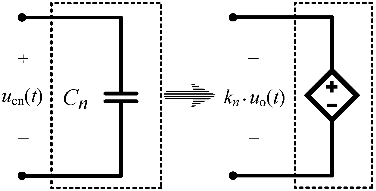
Figure 3.
The topology of the VM converter: (a) the original circuit; (b) the modified circuit by replacing capacitors with controlled voltage sources.
Figure 3.
The topology of the VM converter: (a) the original circuit; (b) the modified circuit by replacing capacitors with controlled voltage sources.
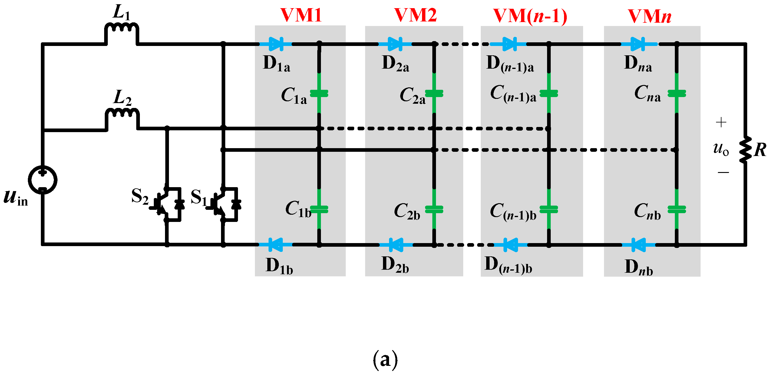
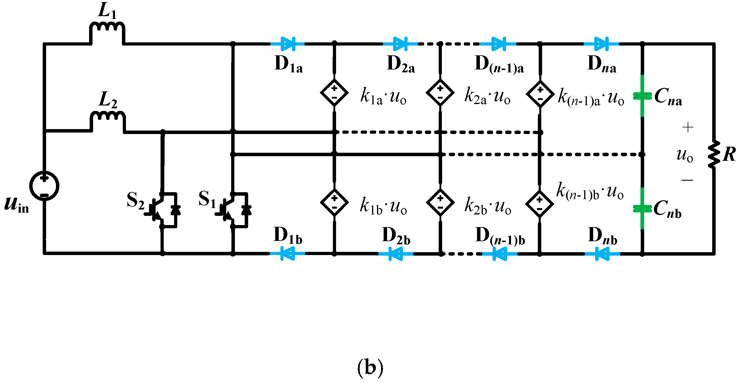
Figure 4.
Three working state equivalent circuits of the VM converter: (a) S1, S2 are both on; (b) S1 is on and S2 is off; (c) S2 is on and S1 is off.
Figure 4.
Three working state equivalent circuits of the VM converter: (a) S1, S2 are both on; (b) S1 is on and S2 is off; (c) S2 is on and S1 is off.
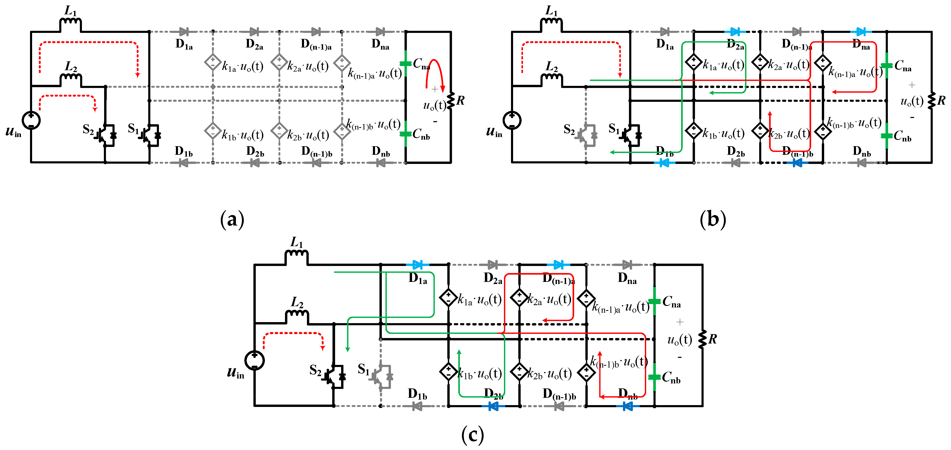
Figure 5.
(a) The reduced-order averaged model of the VM converter; (b) The general reduced-order averaged model of the converters based on VM.
Figure 5.
(a) The reduced-order averaged model of the VM converter; (b) The general reduced-order averaged model of the converters based on VM.

Figure 6.
General small-signal AC model of the converters based on VM.

Figure 7.
VM number is 2 and (a) Cna = Cnb = 0.67 μF, duty cycle changes; (b) Cna = Cnb = 0.67 μF, input voltage changes; (c) Cna = Cnb = 2 μF, duty cycle changes; (d) Cna = Cnb = 2 μF, input voltage changes; (e) Cna = Cnb = 10 μF, duty cycle changes; (f) Cna = Cnb = 10 μF, input voltage changes.
Figure 7.
VM number is 2 and (a) Cna = Cnb = 0.67 μF, duty cycle changes; (b) Cna = Cnb = 0.67 μF, input voltage changes; (c) Cna = Cnb = 2 μF, duty cycle changes; (d) Cna = Cnb = 2 μF, input voltage changes; (e) Cna = Cnb = 10 μF, duty cycle changes; (f) Cna = Cnb = 10 μF, input voltage changes.
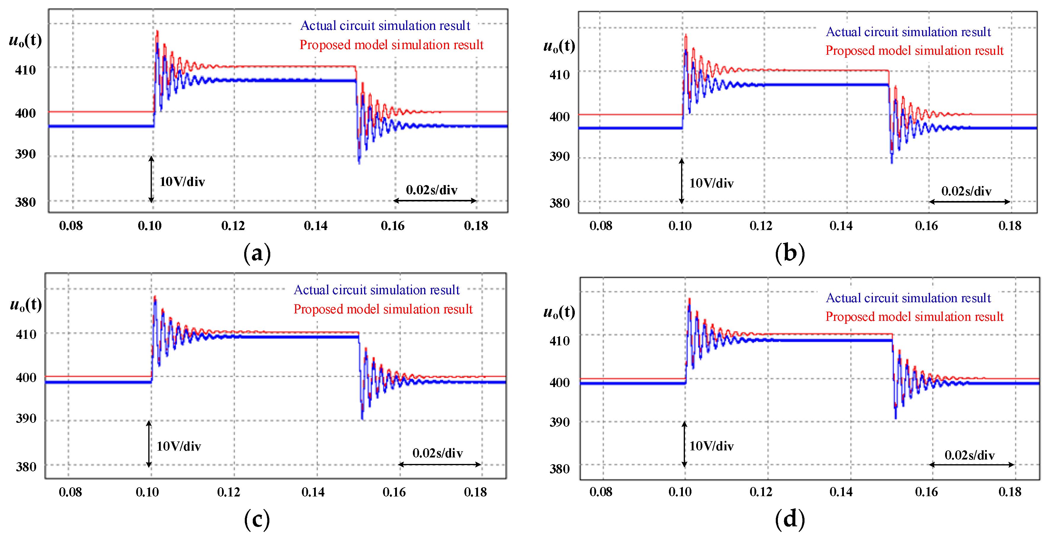

Figure 8.
VM number is 3, Cna = Cnb = 2 μF, and (a) duty cycle changes; (b) input voltage changes.
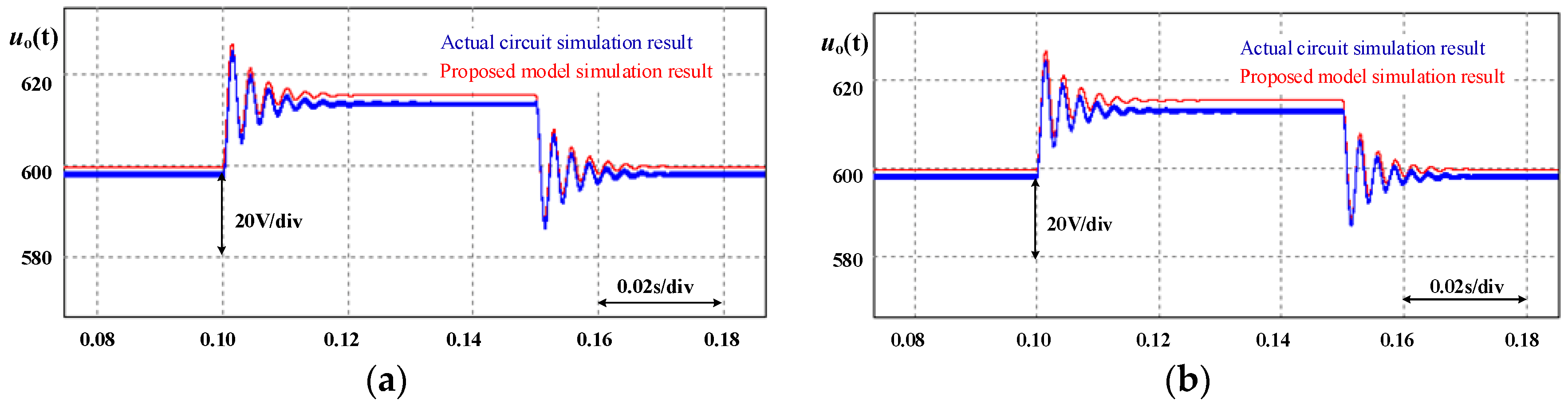
Figure 9.
VM number is 5, Cna = Cnb = 2 μF, and (a) duty cycle changes; (b) input voltage changes.
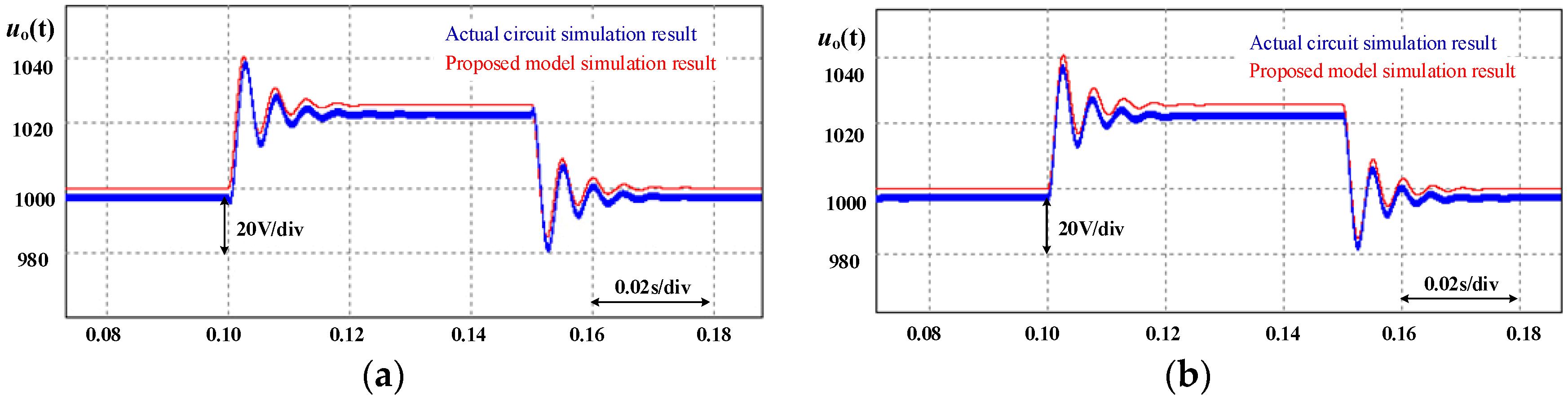
Figure 10.
Voltage control system: (a) for converter circuit with 2 VMs; (b) control schematic diagram.
Figure 10.
Voltage control system: (a) for converter circuit with 2 VMs; (b) control schematic diagram.
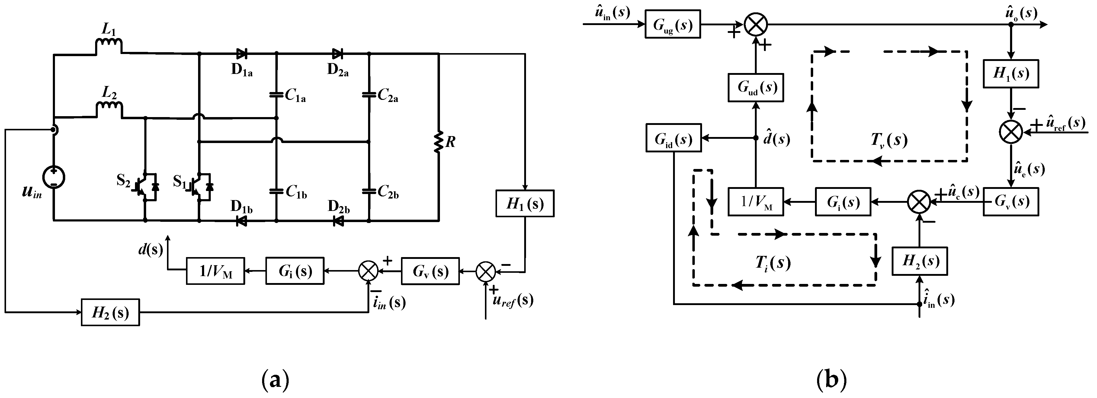
Figure 11.
Frequency characteristic of the current loop gain: (a) without compensation (b) with compensation.
Figure 11.
Frequency characteristic of the current loop gain: (a) without compensation (b) with compensation.
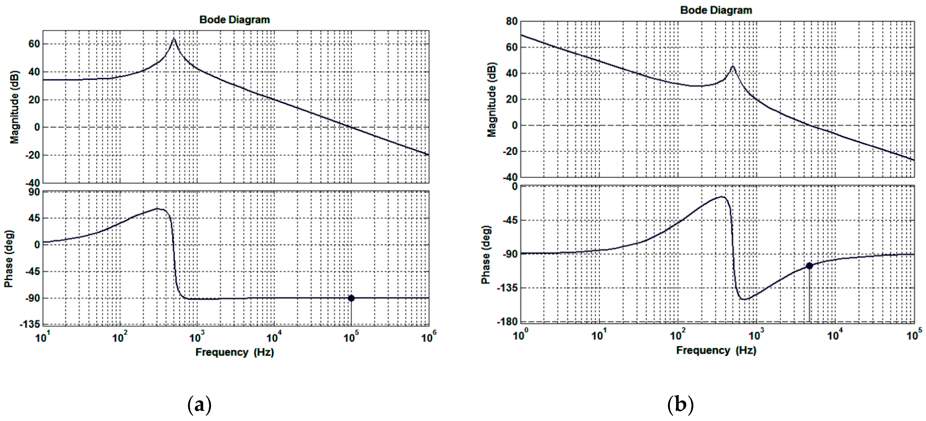
Figure 12.
Frequency characteristic of the voltage loop gain (a) without compensation; (b) with compensation.
Figure 12.
Frequency characteristic of the voltage loop gain (a) without compensation; (b) with compensation.
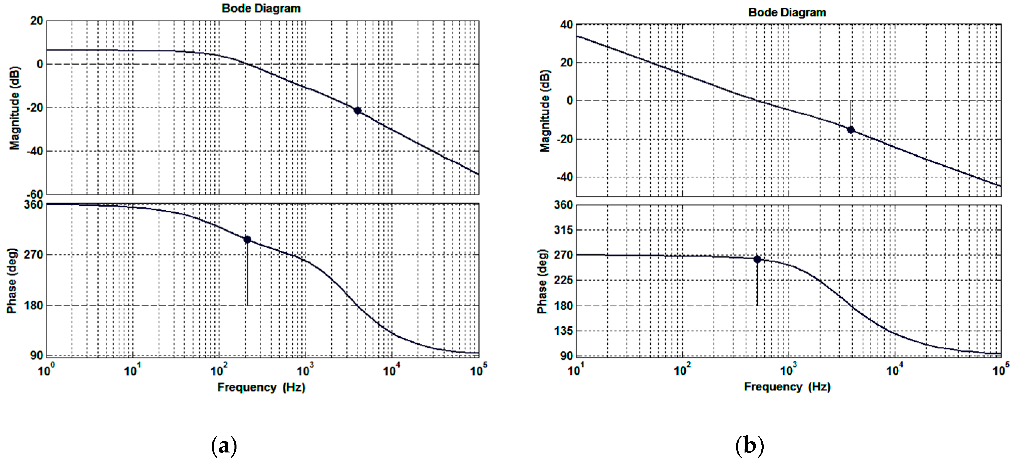
Figure 13.
Comparison of frequency responses of the proposed model (black solid lines) and detailed circuit model (red dashed lines): (a) Bode diagram of Gid(s); (b) Bode diagram of Gud(s).
Figure 13.
Comparison of frequency responses of the proposed model (black solid lines) and detailed circuit model (red dashed lines): (a) Bode diagram of Gid(s); (b) Bode diagram of Gud(s).

Figure 14.
Simulation waveforms for (a) step changes of input voltage; (b) step changes of load resistance.
Figure 14.
Simulation waveforms for (a) step changes of input voltage; (b) step changes of load resistance.
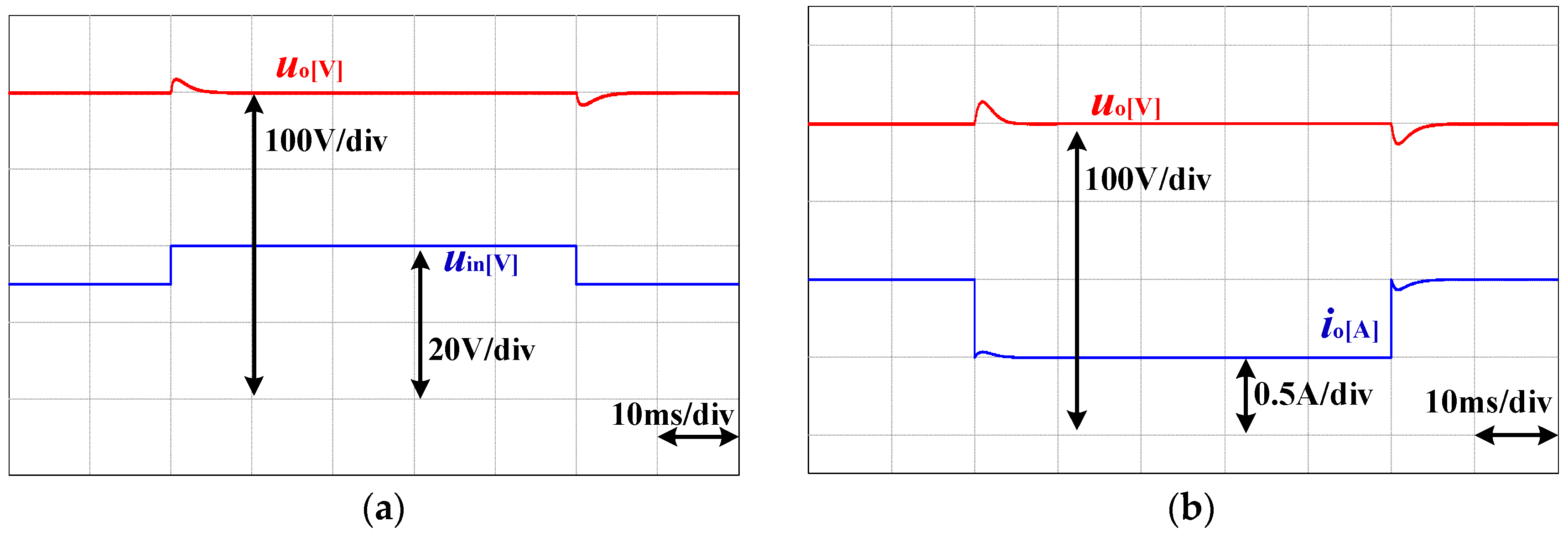
Figure 15.
Hardware experimental prototype.
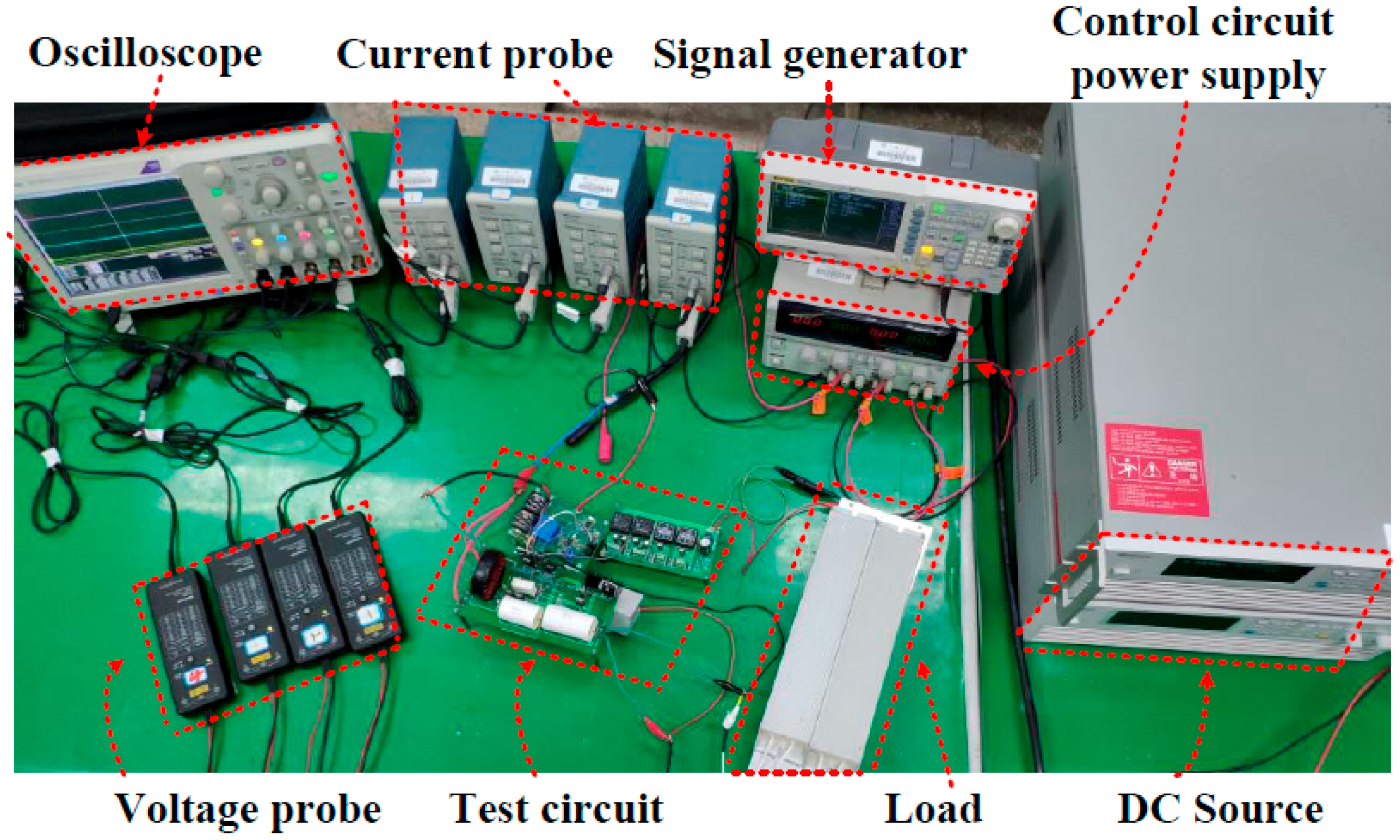
Figure 16.
Experimental waveforms of (a) input voltage increases from 30 V to 40 V with ramp rate of 1 V/ms; (b) input voltage decreases from 40 V to 30 V with ramp rate of −1 V/ms; (c) load resistance increases from 400 Ω to 800 Ω; (d) load resistance reduces from 800 Ω to 400 Ω.
Figure 16.
Experimental waveforms of (a) input voltage increases from 30 V to 40 V with ramp rate of 1 V/ms; (b) input voltage decreases from 40 V to 30 V with ramp rate of −1 V/ms; (c) load resistance increases from 400 Ω to 800 Ω; (d) load resistance reduces from 800 Ω to 400 Ω.


Table 1.
Parameters of the reduced-order average model for different converter circuits based on VM.
Table 1.
Parameters of the reduced-order average model for different converter circuits based on VM.
| Ref. | Topology | Expressions of Equivalent Parameters |
|---|---|---|
| [9] |  | |
| [10] | 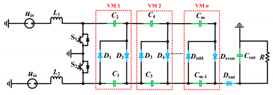 | |
| [11] |  | |
| [14] | 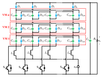 | |
| [16] |  |
Table 2.
Key Parameters of the small-signal AC models for different converter circuits based on VM.
| Reference | A | B | C |
|---|---|---|---|
| [12] | |||
| [9,11,14] | |||
| [10] | |||
| [16] |
Table 3.
Parameters of Simulation and Experimental Prototype.
| Component | Rated Parameters | Extended Parameters |
|---|---|---|
| Switches | GP4055 | GP4055 |
| Diodes | STTH15L06D | STTH15L06D |
| VM number | 2 | 3/5 |
| Capacitors in VM (μF) | 10 | 10 |
| Output filter capacitor (μF) | 10 | 10 |
| L1, L2 (μH) | 320 | 320 |
| Load resistance (Ω) | 400 | 400 |
| Switch frequency (kHz) | 50 | 50 |
| Duty cycle | 0.6 | 0.6 |
| Input voltage (V) | 40 | 40 |
| Output voltage (kV) | 0.4 | 0.6/1 |
| Output power (kW) | 0.4 | 0.9/2.5 |
Table 4.
Parameters of Capacitor Values with Different VM Numbers.
| VM Numbers | Capacitor Values (μF) | Voltage Ripple |
|---|---|---|
| 2 | C1a, C1b: 10 | 2% |
| C1a, C1b: 2 | 10% | |
| C1a, C1b: 0.67 | 30% | |
| 3 | C1a, C1b: 3 | 10% |
| C2a, C2b: 1.5 | ||
| 5 | C1a, C1b: 5 | 10% |
| C2a, C2b: 2.5 | ||
| C3a, C3b: 1.7 | ||
| C4a, C4b: 1.25 |
© 2019 by the authors. Licensee MDPI, Basel, Switzerland. This article is an open access article distributed under the terms and conditions of the Creative Commons Attribution (CC BY) license (http://creativecommons.org/licenses/by/4.0/).
Share and Cite
MDPI and ACS Style
Zhu, B.; Zeng, Q.; Vilathgamuwa, M.; Li, Y.; Chen, Y. A Generic Control-Oriented Model Order Reduction Approach for High Step-Up DC/DC Converters Based on Voltage Multiplier. Energies 2019, 12, 1971. https://doi.org/10.3390/en12101971
AMA Style
Zhu B, Zeng Q, Vilathgamuwa M, Li Y, Chen Y. A Generic Control-Oriented Model Order Reduction Approach for High Step-Up DC/DC Converters Based on Voltage Multiplier. Energies. 2019; 12(10):1971. https://doi.org/10.3390/en12101971
Chicago/Turabian StyleZhu, Binxin, Qingdian Zeng, Mahinda Vilathgamuwa, Yang Li, and Yao Chen. 2019. "A Generic Control-Oriented Model Order Reduction Approach for High Step-Up DC/DC Converters Based on Voltage Multiplier" Energies 12, no. 10: 1971. https://doi.org/10.3390/en12101971
Note that from the first issue of 2016, this journal uses article numbers instead of page numbers. See further details here.