Review

Progress on Crystal Growth of Two-Dimensional Semiconductors for Optoelectronic Applications

State Key Laboratory of ASIC and System, School of Microelectronics, Fudan University, Shanghai 200433, China
*
Authors to whom correspondence should be addressed.
Crystals 2018, 8(6), 252; https://doi.org/10.3390/cryst8060252
Submission received: 1 June 2018 / Revised: 13 June 2018 / Accepted: 13 June 2018 / Published: 16 June 2018

Abstract

:
Two-dimensional (2D) semiconductors are thought to belong to the most promising candidates for future nanoelectronic applications, due to their unique advantages and capability in continuing the downscaling of complementary metal–oxide–semiconductor (CMOS) devices while retaining decent mobility. Recently, optoelectronic devices based on novel synthetic 2D semiconductors have been reported, exhibiting comparable performance to the traditional solid-state devices. This review briefly describes the development of the growth of 2D crystals for applications in optoelectronics, including photodetectors, light-emitting diodes (LEDs), and solar cells. Such atomically thin materials with promising optoelectronic properties are very attractive for future advanced transparent optoelectronics as well as flexible and wearable/portable electronic devices.

1. Introduction

The continuous complementary metal–oxide–semiconductor (CMOS) scaling to achieve more powerful integrated circuit systems is reaching fundamental limits imposed by heat dissipation and short-channel effects. Extensive motivation and stimulated efforts have been shown towards both device units and integration technology to slow down the deviation from the trend predicted by Moore’s law. Recently, two-dimensional (2D) semiconductors such as graphene, transition metal dichalcogenides (TMDCs), and black phosphorus (BP), which consists of one or a few atomic layers have been intensively investigated for their intrinsic ultrathin body and robust lattice structure. They have been considered to represent the ultimate state in scaling and are believed to possess superior potential applications in future integrated circuit, memory, and optoelectronics. The significance of such materials has been increasingly recognized with the inevitable slow-down in CMOS scaling when the lithography scale approaches atomic dimension. So far, 2D semiconductors have been largely acquired through experimental research focusing on the exfoliated thin films from bulk crystals (including the “scotch tape” method and lithium-based intercalation) for the study of physical and material properties, such as the band structure [1,2,3,4], valleytronics, and spintronics [5,6,7,8], electronic and optical properties [9,10,11], doping [12,13], strain, temperature dependence [14,15,16] and heterostructures [17,18]. Mechanical exfoliation has been proved to be a fast and easy way to fabricate high crystal quality few-layer or even single-layer 2D samples, since these atomic layers are bonded by van der Waals interactions. In contrast, more integrated circuit-targeted fabrication approaches such as chemical vapor deposition (CVD), physical vapor deposition (PVD), and atomic layer deposition (ALD) have privilege in creating uniform wafer-scale films on various substrates. Although the crystal quality and subsequent device performance is inferior to the exfoliated samples, these CMOS-compatible fabrication techniques are essential in realizing the practical application of the 2D materials in future electronic devices. Therefore, to achieve stable, high-quality, and large-area growth of 2D materials and to establish integrated circuits based on the implementation of homogeneous device units, they have been widely pursued in recent years.
Optoelectronic devices that can generate or sense light, or produce electric signals are important components in future optical-electrical, sensing, and energy-storage systems, such as light emitting diodes (LED), lasers, photodetectors, and solar cells. 2D semiconductors are intrinsically attractive in such applications due to their proper electronic band structures and ultra-thin body with scaling capabilities. Graphene with a single layer of carbon atoms in a honeycomb structure (schematically shown in Figure 1a), has impressively high electron mobility owing to its distinctive bands [19]. However, the lack of intrinsic band gap limits the further application in electrical devices. Up to now, there has been no mature or well-controlled method to open up a gap in graphene and maintain the electronic mobility at the same time [20]. However, graphene has been identified as a promising candidate in optoelectronics, specifically in high-frequency optoelectronic application with the reported photodetector bandwidth up to GHz [11,21]. On the other hand, TMDCs which typically have a general formula of MX2 (M = Mo, W, Re, etc.; X = S, Se, Te) have thickness-dependent band gaps from 0.5 eV to 2 eV. Figure 1d and 1e illustrate the band structures of several typical TMDC semiconductors. For most TMDC materials like MoX2 and WX2, the band gap shows a similar indirect-to-direct transformation with decreasing thickness. One exception is ReS2 which possesses a direct band gap for both monolayer and multilayer/bulk (Figure 1c) [22]. Therefore, TMDCs can be expected to exhibit good optoelectronic response in the near-infrared to visible spectral region. BP is a newly-discovered and stable semiconducting allotrope of phosphorus (structure shown in Figure 1b) whose intrinsic hole mobility can be as high as 300–1000 cm2V−1s−1 at room temperature [23,24], and the on-state current density can reach 850 μA/μm [25]. However, the device performance of BP field-effect transistor (FET) is still far below the standards of practical application owing to the fact that BP can be easily oxidized by O2 and H2O at ambient [26,27]. Monolayer BP has a direct band gap of 2 eV at the gamma point of the first Brillouin zone. The band gap reduces with increasing thickness, and finally reaches 0.35 eV for bulk BP [28,29,30], resulting in attractive optoelectronic applications from the infrared to the visible region. In this paper, we review the development of approaches to synthesize thin films of 2D semiconductors, while presenting further strategies to extend their applications in future high-performance optoelectronic devices.

2. Crystal Growth of 2D Semiconductors
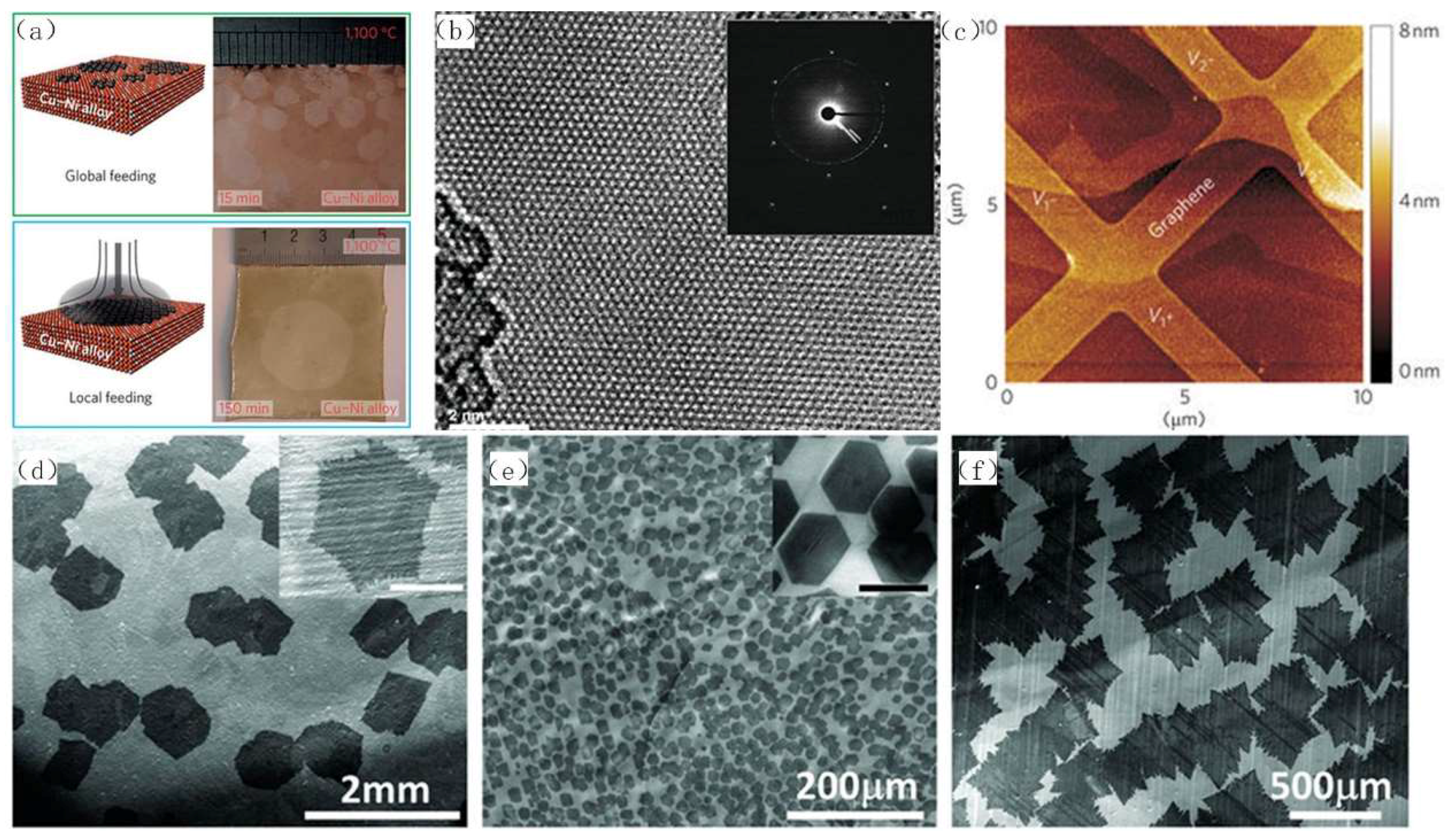
The synthesis of 2D materials could be categorized into two groups: top-down strategy, including mechanical exfoliation and lithium-based exfoliation; and bottom-up strategy, like physical vapor deposition (PVD), chemical vapor deposition (CVD), and atomic layer deposition (ALD) to synthesize thin films. As discussed above, mechanical exfoliation is more advantageous in fabricating high-quality crystalline thin films with fewer defects. Nevertheless, the small lateral size and the lack of sample reproducibility and controllability in film locations and thickness make this approach unsuitable for large-scale device integration. Chemical methods such as lithium-based exfoliation and annealing could produce uniformly distributed graphene flakes in large volume. However, it is hard to control the number of layers on the whole substrate and avoid organic contamination so chemical methods are preferred in producing dielectrics and decoration layers. A synthesis method to produce reproducible, uniform, low-defect, and large-scale 2D semiconductor thin film is the prerequisite to enable practical electronic and optoelectronic applications. In this section, we review the crystal growth of 2D materials with a focus on the bottom-up synthesis for high-quality large-area thin films, including graphene, transition metal dichalcogenides, black phosphorus, and heterojunctions of different 2D materials.

2.1. Graphene

Graphene can be categorized based on its lateral extension including sheets and flakes for dimensions larger than 100 nm, along with quantum dots and nanoribbons for small dimensions. The graphene exhibits no bandgap which means it is not suitable for semiconductor device applications. However, the material properties of graphene can be engineered with a bandgap as the film thickness is below 10 nm based on the quantum confinement effect. Moreover, graphene nanoribbons and quantum dots also exhibit high carrier mobility in addition to the proper bandgap. It has been recognized that the production of wafer-scale single crystalline graphene film is a key factor to realize graphene-based optoelectronic devices. Typically, CVD is the most commonly used method for the epitaxial growth of graphene. The graphene synthesized by this approach is typically polycrystalline which suggests the depression of electronic characteristics. Hence, the CVD growth of graphene is often performed on a single-crystalline surface which functions as catalyst. Different metals have been studied for the catalytic growth of graphene including Ni [33], Cu [34,35,36,37], Mo [38], Pt [39], and Ru [40]. Single crystalline graphene with size up to 1 cm can be achieved on Cu substrate [37] and the film with ~4 cm in size has been demonstrated on Cu–Ni alloy substrate with optimized conditions [41], as displayed in Figure 2a. Although such preparation of large-area graphene film using metallic catalysts has been widely adopted for various nanoelectronic device research studies, it is more appealing to optoelectronics to achieve direct synthesize of graphene on the substrates without a catalyst since it can avoid contamination from metal, metal etchant, and Polymeric Methyl Methacrylate (PMMA). New types of substrate, for instance, Ge [42] (Figure 2b) and SiC [43] (Figure 2c), have been tested for the non-catalytic growth of single crystalline graphene. SiC substrate has been demonstrated with a high mobility of 500–2000 cm2V−1s−1 with a Si-terminated surface [43]. Despite the substrate types, advanced growth mechanism such as the plasma-enhanced CVD (PECVD) has also been proved to be useful in obtaining graphene at low temperature without metallic catalysts. Epitaxially grown single-crystalline graphene with high-quality has been reported on hexagonal boron nitride (h-BN) using PECVD [44]. The growth of graphene can also be modulated by oxygen atoms on the surface (Figure 2d–f) [37].Generally, the size of graphene layer is restricted by the grain size and the structure of substrate material. Therefore, substrates with a hexagon structure are much more advantageous in growing larger size single-crystalline graphene.
As mentioned above, graphene quantum dots (GQDs) and nanoribbons (GNRs) can enable the further engineering on the properties of graphene specifically the band structure for optoelectronic applications. In research, bottom-up synthesis is usually adopted which is based on oxidizing organic precursors, such as oxidative cyclodehydrogenation of oligophenylene and polyphenylene [45]. It should also be mentioned that a variety of precursors have been employed for the synthesis of graphene, such as ethylene, usually with the assistance from hydrogen at ambient [46]. Paternò et al. have reported the synthesis of a novel graphene molecule, namely dibenzo[hi,st]ovalene (DBO 1) which has remarkable stability in the atmosphere [47]. The photoluminescence quantum yield (PLQY) of this molecule can reach up to 79% with very low energy consumption. This leads to potential applications in LED and laser devices. In general, organic synthesis approaches are more expensive while luminescence GQDs can be produced by hydrothermal methods as well. Although it is hard to control the film thickness and quality during the hydrothermal process, it is a low-cost approach to obtain graphene nanoparticles [48]. On the other hand, the optical bandgap of GNRs ranging from 1 eV to 2 eV can be modulated through different width and edge structure. Both armchair and zigzag edge structures are available and each type can have many forms. Different GNRs have been studied exhibiting different electrical properties by varying the precursors [49]. Also, introducing ion dopants, such as nitrogen, sulfur, and boron, can influence the electrical properties of GNRs, thus providing another method for engineering GNRs [50,51,52].

2.2. Transition Metal Dichalcogenides

Generally, the growth of high-quality and uniform transition metal dichalcogenide (TMDC) films is far more difficult than that of graphene. This also explains the fact that most of the current research on TMDCs is based on the mechanically exfoliated ultra-thin flakes and films. The grain size and electrical properties of the synthetic films are still needed to be improved to satisfy further electronic applications. Among all the studies and reports on TMDC growth, CVD is still the most popular and reliable method for bottom-up synthesis of TMDCs. Up until now, many TMDC films have been achieved by CVD including MoS2 [53,54,55,56,57], WS2 [58], MoSe2 [59], WSe2 [60], MoTe2 [61], and ReS2 [62,63]. These synthesis methods can be categorized into solid-phase precursor growth and gas-phase precursor growth. Solid-phase precursors are basically composed of sulfur powder and metal-oxide powder. Precursors are placed with the substrate together in line within the reaction tube furnace. In this way, TMDC flakes are grown on the substrate with well-controlled thickness and decent electrical properties (mobility around ~50–100 cm2 V−1 s−1) [53]. In addition, spatial and size uniformity of TMDC flakes can be improved by the pretreatment of substrates (Figure 3a–c) [64]. However, the nucleation sites for TMDC growth are random on the substrate and it is hard to eliminate the grain boundaries which usually lead to poor wafer-scale quality of synthesized TMDC film. Besides, the CVD process can be performed by solid-phase TMDC powder alone (as shown in Figure 3d–f), but the electrical and optical quality are not good enough [65]. In addition, as shown in Figure 3g–k, a high fabrication yield of (99.5%) for MoS2 and WS2 thin films was realized by Kang et al. with good mechanical strength and film continuity on the basis of metal–organic chemical vapor deposition (MOCVD) [66]. The precursors used for MoS2 and WS2 thin films in their work were Mo(CO)6/(C2H5)2S and W(CO)6/(C2H5)2S, respectively. Atomic layer deposition (ALD) is also available for TMDC films and many kinds of TMDC films have already been reported including MoS2 and WSe2 [67]. The films obtained by this method exhibit poor crystalline property due to the low temperature nature of the ALD process, thus limiting the application in optoelectronic devices.
“Two-step” growth using CVD is also popular for the large-scale synthesis of TMDCs. This process usually begins with the deposition of a layer of transition metal or its relative compound (oxides) on the substrate, followed by sulfurization, selenization, or other high-temperature treatment [68,69]. PVD is a handy method to deposit metal or its compounds on the substrate and probably forms inhomogeneous mixtures of monolayer, multi-layer, and non-deposition region within one wafer. So, the roughness of these films grown by PVD is typically higher than CVD/ALD. The domain sizes are also much smaller than the solid-phase precursor-based CVD films. On the other hand, sulfurizing metal oxide films prepared by ALD has recently been identified with better step coverage and more precise thickness control in wafer-scale TMDC thin film (Figure 3l–n). Spatially inhomogeneous mixtures of monolayer, multi-layer, and non-deposition region on the wafer could be avoided. Nevertheless, as mentioned above, the crystallinity of the ALD-involved films and the device performance still need to be improved [70]. Although wafer-scale uniformity could be achieved in various synthesis methods as discussed above, the growth of high-quality large-area single crystal thin film is still the main challenge for further nanoelectronic applications of TMDCs. Han et al. reported an alternative approach, in which the deposition of a seed layer enables selective growth of single crystalline TMDCs at controlled spatial locations (shown in Figure 3o) [71]. This provides more insight on the growth mechanism of TMDCs and the potential solution towards high-quality large-area TMDC thin film growth for optoelectronic applications.

2.3. Black Phosphorus

Stable p-type black phosphorus (BP) is a newly discovered 2D material and was first integrated into a field-effect transistor platform in 2014 [24]. The electronic and optical properties of BP are still under investigation, and most BP devices reported recently are fabricated based on mechanical exfoliation instead of bottom-up synthesis, which ensures that these devices could have the best performance. There are still very few researches on the synthesis of BP, with only one reproducible two-step synthesis method towards large-area BP: depositing a red phosphorus thin film and converting it to BP in a high-pressure environment at room temperature. Li et al. demonstrated a thin-film BP transistor with a hole mobility around 0.5 cm2 V−1 s−1 in 2015, which is one of the earliest reports on the growth and application of large-area BP [72]. In 2016, Smith et al. reported a two-step synthesis approach and obtained a four-layer BP film with average areas >3 μm2 and thicker samples with average areas >100 μm2 [73]. A BP-based photodetector can also be made by inkjet printing for optoelectronics [74]. Unfortunately, high-quality wafer-scale BP thin films are still unseen.

2.4. Heterojunction

The semiconductor heterojunction is a promising architecture for optoelectronic applications and has been widely investigated. For 2D materials and systems, both mechanical exfoliation and epitaxial growth methods can be adopted to form the hetero-structure. Typically, mechanical exfoliation is used to form a van der Waals heterojunction only in vertical geometry. The stacked heterojunction can be more easily obtained than epitaxial growth but with sacrifice on the interfacial quality and orientation controllability. Type II band alignment can be observed in the heterojunction of two different 2D semiconductors. Both simulation and experiments have revealed that the intrinsic 2D van der Waals hetero-structure can behave like p-n diodes, exhibiting remarkable spatial direct optical absorption and emission which suggests promising application in optoelectronics devices such as photodetectors and LED devices [6,75]. So far, different heterojunction with combinations of various 2D materials have been investigated including WS2/MoS2 [76], WSe2/MoS2 [77], GaTe/MoS2 [78], BP/MoS2 [79], SnS2/MoS2 [80], WSe2/MoSe2 [81,82], NbSe2/WSe2 [83], graphene/WS2 [84], WSe2/SnS2 [85], ReS2/WS2 [86] etc. On the other hand, the epitaxial growth of the heterojunction can provide more options and control in the growth direction both in the vertical and lateral. Such growth can be easily achieved by CVD epitaxial at the edge of the surface or domain of one TMDC material, owing to the small lattice mismatch among TMDCs. The vertically stacked hetero-structure has been successfully synthesized by a layer-by-layer epitaxial [87], and laterally stacked hetero-structure synthesis method though single-step CVD approaches have also been reported recently (examples illustrated in Figure 4a–e) [76,77,80,81,88,89]. Basically, heterojunctions are synthesized with solid phase metal oxide and sulfur power. A sharp and clean interface can be obtained, but the thickness and distribution of heterojunctions are random. Recently, Gong et al. reported a two-step CVD epitaxial method of WSe2/MoSe2 heterojunction with both vertical and in-plane epitaxial growth. It is possible to control epitaxial orientation with different growth temperatures and as shown in Figure 4b, c and d, the domain size is much larger than that of the previously mentioned one-step approach [82]. Similar approaches have been used to grow SnS2/WSe2 heterojunction (Figure 4f,g) [85]. Compared to the manually stacked heterojunctions, the CVD epitaxial method can be evolved into a promising application in optoelectronics devices with a high-quality hetero-structure. Moreover, not all the strategies to achieve high-quality hetero-structure have been fully explored, and there are still many more methods to be tested and optimized for further improvement.

3. Applications of 2D Materials in Optoelectronics

As mentioned above, there are many approaches for the crystal growth of different 2D semiconductors such as graphene, black phosphorus, and TMDCs. Heterostructures of 2D materials have also been introduced due to their unique optoelectronic properties. In this section, we introduce their optoelectronic device applications to achieve more insights into these materials and their structures. Typical optoelectronic devices including photodetectors, light emitting diodes, and solar cells based on the 2D materials and heterostructures will be briefly discussed.

3.1. Photodectors

A photodetector is a kind of optoelectronic device that can translate optical signals into electrical signals, such as current, voltage, resistance etc. Many materials and structures including quantum dots [90,91,92], nanotubes [93,94,95,96], and nanowires [97,98,99] have been studied and considered to be good alternatives for silicon-based photodetectors. Interestingly, most of the 2D semiconductors are sensitive to light, heat, and ambient which makes them very attractive for applications in optoelectronic device sensing from infrared to the ultraviolet regime. Technically, parameters used for the evaluation of photodetector performance typically include response wavelength, absorption fraction, internal quantum efficiency (IQE), external quantum efficiency (EQE), photoresponsivity, time constant, bandwidth, on/off ratio of photo-current and dark current, power consumption, and noise equivalent power. The optical property of a material is determined by the response wavelength and absorption rate. Generally, gap-less graphene works in the infrared wavelength region while TMDCs and BP can be used from the ultraviolet to the visible length region due to their thickness-dependent bandgaps, ranging from 0.5 eV to 2.3 eV. Single layer TMDCs and BP usually have a higher absorption and emitting fraction due to their direct bandgap nature. The sensitivity can be quantified by IQE, EQE and photoresponsivity. EQE can be described by the following equation:
EQE = (Iph/q)/(Pin/Eph)
where Iph is the photocurrent, q is the electron charge, Pin is the power of incident light, Eph is the energy of incident photon. IQE equals EQE divided by absorption fraction. Photoresponsivity is equal to the photocurrent divided by the power of incident light: R = Iph/Pin. The response speed is related to the time constant and bandwidth. Regarding the design of modern integrated circuits, a bandwidth of gigahertz is necessary. On and off ratio along with noise power consumption determine the probability that a signal will be misread. Also, power consumption is another important property of a photodetector. 2D semiconductor-based photodetectors can be basically categorized into two types: single channel type and junction type. Single channel type include n-type and p-type, while junction type usually includes homojunction and 2D van de Waals heterojunction photodetectors.

3.1.1. Single Channel Photodetectors

The main mechanism of the single channel type photodetector is photoconductive and photovoltaic. Koppens et al. and Furchi et al. have discovered and explained the mechanism of graphene and n-channel MoS2 photodetector in detail [100,101]. Graphene based photodetectors are dominated by the photo-thermoelectric effect and the bolometric effect. The photo-thermoelectric effect is observed in both graphene p-n junctions and suspended graphene. Hot electrons can be generated by the photo-thermoelectric effect which will produce a positive photovoltage in the channel resulting in fast electric response. The bolometric effect is reflected by the change in the channel conductance produced by the incident photon induced heat leading to a very sensitive nature for photo detecting. As a result, graphene has great potential to be applied in the terahertz range. Graphene can provide ultrafast (~ps) electric and optical signal response, and it can be used as photoconductive channel in the wavelength of the infrared region [11,102,103,104,105,106,107], as well as flexible transparent electrodes in other fast speed photodetectors [108,109,110,111]. Xia et al. reported an ultrafast graphene photodetector with bandwidth up to 40 GHz, with further analysis suggesting an intrinsic bandwidth exceeding 500 GHz [11]. A very fast response graphene photodetector has already been achieved with stable photo current across optical band communication (Figure 5i–k) [104].
For TMDCs and BP, the photovoltaic effect influences their optoelectronic performance by shifting the threshold voltage in either the negative (n-type) or positive (p-type) direction indicating extremely high photoresponsivity in direct (DC) circumstances [100]. The photoconductive gain, typically induced by the trapping of charge carrier, can provide response to optical signals with frequencies ranging between 1 kHz to 3 kHz (Figure 5a,b) [100]. The time constant of TMDCs and the BP single channel photodetector is commonly between several milliseconds to hundreds of seconds (one example of WS2 photodetector shown in Figure 5c,d) [10,112,113,114,115,116,117]. Hence, these photodetectors can be potentially applied in a low light intensity and frequency device, while photo-electron gain is mainly contributed by the photovoltaic effect when the time constant is large. The N-channel exfoliated monolayer MoS2 detector was first demonstrated in 2011 [118] and was then studied widely with typical photoresponsivity as high as hundreds to thousands AW-1 in the depletion region and 100 times higher in the accumulation region in the DC test (Figure 5e,f) [10,119]. Wu et al. reported a few layer BP phototransistor possessing responsivity of 90,000 AW−1 in the ultraviolet wavelength [117]. Some reports demonstrated photodetectors with much faster response in the absence of high gain of weak light beam (commonly on the order of mAW−1), with the bandwidth below 10 kHz (Figure 5g,h) [117,120]. A single channel photodetector whose channel is a metal diselenide compound possessed a balanced performance exhibiting faster optical response than disulfide (commonly ~100 Hz), but lower responsivity in the visible wavelength. Other exfoliated 2D TMDCs such as WS2 [121,122], GaSe [123], GaS [124], ReS2 [115,125], In2Se3 [98,126,127], MoSe2 [128], GaTe [129] have also been reported in high gain n-channel photodetectors. Mobility of these synthetic materials and the quality of the semiconductor/oxide interface are very important for photodetectors based on the CVD method, while the device fabrication process is almost the same as that on exfoliated films. Wide wavelength response in the infrared region and fast response speed could be obtained with the CVD method [102,110,117,130]. Wafer-scale graphene-based photodetectors are usually fabricated by CVD on copper film and then transferred onto the desired substrate. For TMDCs, single channel photodetectors, CVD synthesis with solid-phase metal oxide and sulfur precursors are widely used because of the easy synthesis approach, large single crystal domain, and high mobility. Photodetectors based on CVD MoS2 [113,131], MoSe2 [132,133], ReS2 [63,114], ReSe2 [134], SnS2 [135,136], SnSe2 [137], and WS2 [110,122] have been studied recently. Jing et al. reported a MoS2 phototransistor array that can detect room light illumination [138]. However, comparing to exfoliation flakes, the performance of CVD TMDCs photodetectors still requires more improvement for both responsivity and speed. Table 1 lists and compares the fabrication method and device performance of the recently reported single-channel 2D material-based photodetectors.

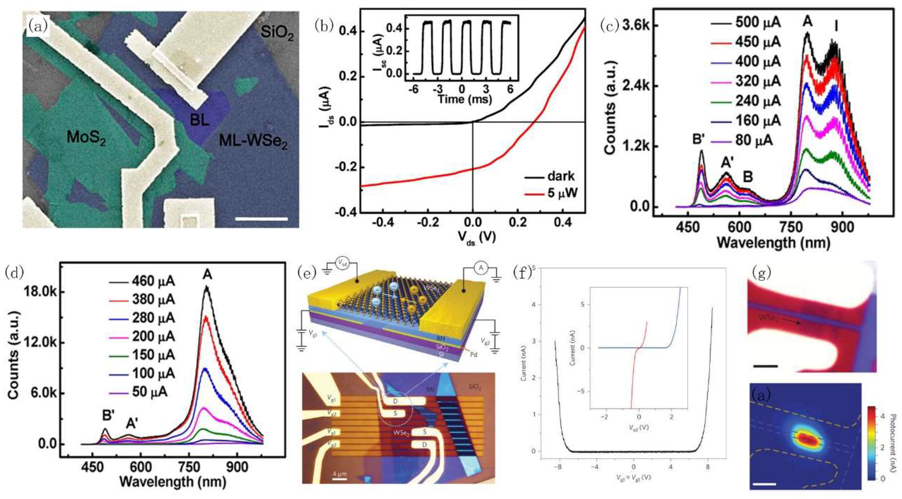
3.1.2. Junction Type Photodetectors

The current of junction type photodetectors is mainly generated by photo-excited carriers. Most of the 2D semiconductors are intrinsic n-type at atmosphere, but some semiconductors, for instance BP, WSe2, GaTe, can provide competing mobility under specific circumstances. Besides, the advanced doping method is necessary to obtain the homo-structure p-n junction. However, p-type doping strategy for n-type 2D semiconductors has many limitations now and quite a few approaches have been tried on various materials including graphene [21], WSe2 [140], etc. The metal contact method works well only near the Schottky barrier, while electrical gate controlling is only valid in a certain bias range. Molecular absorption and chemical doping are not stable or sufficient regarding the mobility and on/off ratio [21,140].
Heterojunctions can be easily formed by transferring and stacking exfoliated 2D materials vertically. High-performance exfoliated and transfer-stacked heterojunctions like WS2/MoS2, WSe2/MoS2, WSe2/MoSe2, graphene/TMDC photodetectors have been extensively studied and reported with high EQE (up to 278%) and fast response (up to 100 GHz) [109,142,143,144,145]. However, it should be noted that, although the optical and electrical properties of transferred heterojunctions are usually superior to those formed by CVD methods, polymer contamination can deteriorate interfacial quality during the transfer process. On the other hand, both vertical and lateral heterojunctions can be formed using CVD methods enabling more structural options for photodetectors. Photodetectors based on CVD TMDC heterojunctions have been experimentally demonstrated recently [80,82,88,146,147]. The photoresponsivity is high in these photodetectors (EQE = 50%–300%), but the time-resolved photo response is not satisfactory as the maximum response frequency is only in the range of Hz to kHz. Son et al. report optoelectronic properties of the heterojunction with metallic NbSe2 and semiconducting WSe2 [83]. The heterojunction is achieved by selenization of pre-deposited Nb2O5 and WO3 on SiO2/Si substrate, as shown in Figure 6a. Different photo current response behavior is observed with exposure to different light wavelengths (Figure 6b,c). Kim et al. demonstrated an approach to form the p-n junction of WS2/p-Si via sputtering (Figure 6e–g) [143]. The junction exhibits good self-biased ultraviolet (UV), visible. and Near-infrared region (NIR) detection ability. The photo response speed is 1.1 μs which is better than the silicon-based photodetector, as shown in Figure 6h,i. The WS2/p-Si junction also possesses high wavelength dependent linear dynamic range (LDR) ranging from 52 dB to 90 dB (Figure 6d), which means it can provide very good image quality. It should also be mentioned that, as compared with the single channel device (MoS2 or MoSe2), MoS2/MoSe2 heterojunction exhibits better photo response performance, which is further demonstrated in Figure 6j–n [146].
Graphene–TMDC heterojunction photodetectors, based on the solid-phase CVD and transfer process, exhibit high responsivity in low frequency circumstances [107,117] . Another interesting stacked photodetector structure is based on 2D material combined with other traditional p-type semiconductors, such as p-Si, p-Ge and p-GaN [105,148]. Several researches are based on pn-diode photodetectors of CVD graphene/Si and CVD TMDC/Si and show excellent optical response [149,150,151]. For example, An et al. reported a tunable graphene/p-Si heterojunction photodetector in the frequency of MHz [150]. The internal quantum efficiency reached 65%, and the photoresponsivity was about 107 VW−1 in the visible and infrared region. Table 2 lists and compares the fabrication methods and device performances of the recently reported junction-type photodetectors.
In conclusion, 2D semiconductors have a huge potential in photodetector applications. Graphene-based photodetectors usually demonstrate excellent performance in the infrared wavelength region and high speed optical response. TMDCs and BP based photodetectors have high photoresponsivity in the ultraviolet and visible region. Junction-type photodetectors have lower optical gain but much faster response than single channel photodetectors. So far, there is still a large gap in optoelectronic properties between 2D semiconductors synthesized by the CVD method and exfoliated flakes. The photoresponsivity of the CVD device is only about one-tenth of the exfoliated counterparts, and the response speed also needs improvement. So, there are still many investigations to be carried out to achieve satisfactory photodetectors by CVD synthesized TMDCs.

3.2. Light Emitting Diode
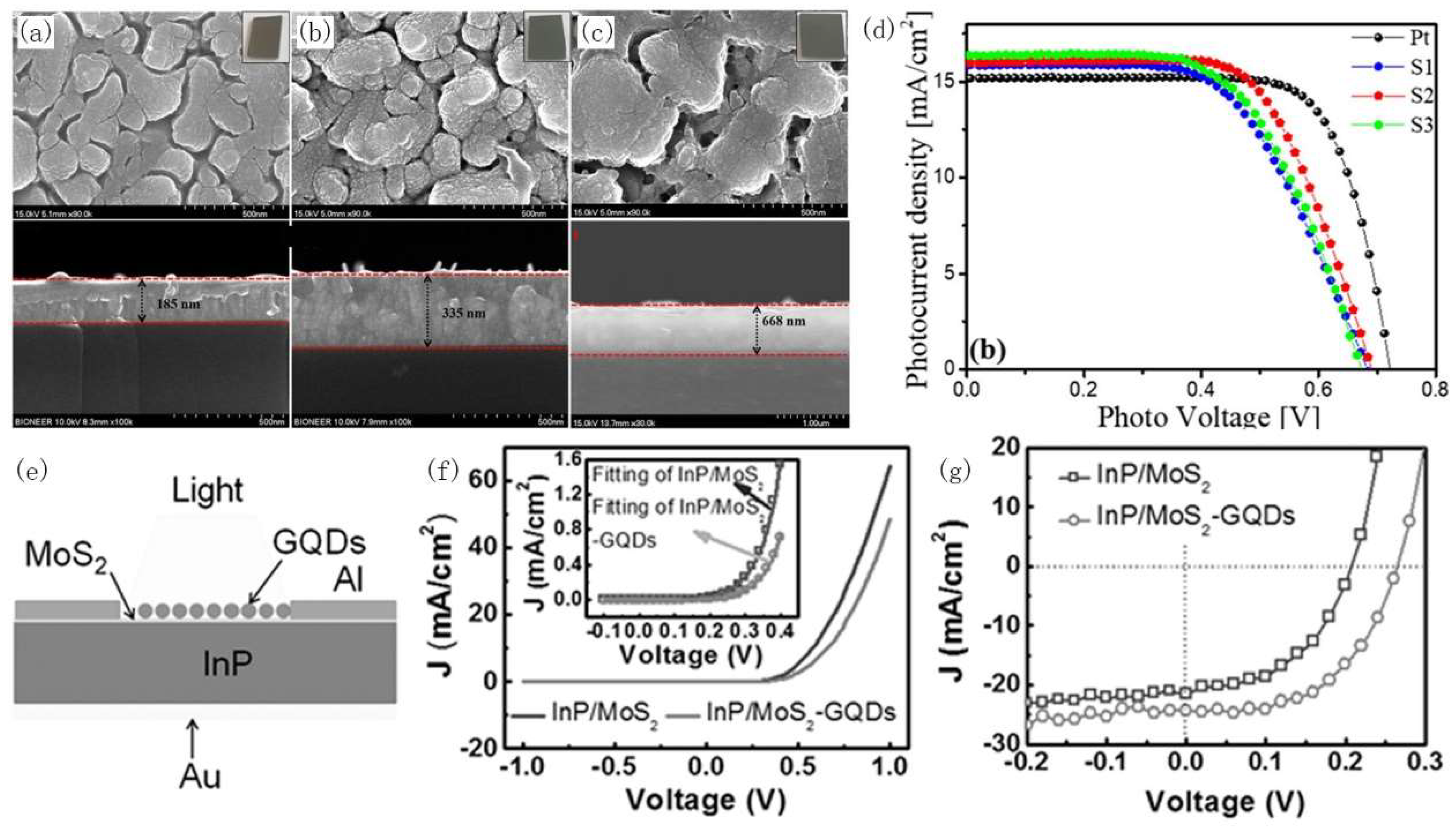
Both homojunctions and heterojunctions of 2D van der Waals materials can be used in light emission diodes (LEDs) except for gapless graphene. The most widely reported materials are monolayer TMDCs with direct bandgap, for instance monolayer MoS2, MoSe2, and WSe2 [152,153,154,155,156]. Devices have been fabricated into the homojunction structure [140,153,157], the lateral heterojunction structure [76,88], and the vertical heterojunction structure [158,159]. Although light emitting behaviors induced by both the source drain electrical field and photons are commonly observed in direct bandgap TMDC junctions, high-efficiency LED and laser devices have still been rarely reported. Back-gate structured lateral homojunction LED devices made of monolayer WSe2 with source drain doping have been studied, and the EQE is around 0.1%–0.5% in these LEDs (shown in Figure 7e–g) [153,157]. Besides, Zhang et al. demonstrated the unique valley-dependent optoelectronic properties of WSe2 homojunction [160] . WSe2 p-n diode will be created with back gate and source drain bias, while the electroluminescence spectrum (EL) spectrum is mainly affected by the orientation of the WSe2 crystal.
Most LED and excitonic devices with TMDC materials are fabricated by using the transfer-stack method. For the CVD epitaxial approach, lateral heterojunctions are easy to achieve, while the emitting area is smaller and the contact resistance is larger than for vertical heterojunctions. So the vertical heterojunction LED is more promising with regard to higher current density and brighter emitting light [154]. Wither et al. demonstrated the 2D van der Waals transfer stacks consisting of graphene electrodes, boron nitride dielectric, and TMDCs as emitters [154]. The EQE is as high as 10% in 3 to 4 multiple stacks. LEDs based on Schottky diodes usually have low EL intensity, and the EQE is in the order of 0.01% [155,160] . Cheng et al. reported the EL spectra of a vertical stack of PVD WSe2/exfoliated MoS2 diode (Figure 7a–d) [158]. The diode exhibits good light emitting capability with light wavelength from 750 nm to 1000 nm. The EQE of the diode is as high as 12%, which is the highest among LED and excitonic devices made with 2D semiconductors. Other LED devices fabricated by CVD 2D semiconductors have been hardly reported largely because of poor emitting efficiency. Table 3 lists and compares the fabrication method and device performance of the recently reported 2D LED devices.

3.3. Solar Cell

Solar cells are devices which can directly convert light to electricity based on the photovoltaic effect. The solar cell is a very competitive and fastest growing candidate for renewable energy source. However, solar cell technology is not an absolute green technology. Most of the greenhouse gas of solar cells is generated during the manufacturing phase and the recycling of the solar cell is also an issue which is of concern. Moreover, efficiency is the most important characteristic since it represents the capability of converting light to electricity. An ideal solar cell device should be environmentally friendly during the manufacturing process, especially without toxic compounds for the sake of recycling. The efficiency should be as high as possible and a longer lifetime is more desirable.
Solar cell devices can be characterized by open-circuit voltage (Voc), short-circuit current density (Jsc), fill factor (FF), and power conversion efficiency (PCE). Voc demonstrates the built-in potential field across the solar cell. Jsc is the generated current density and it can be affected by the absorption ability of light. FF is the index of loss electric generation. PCE is the ratio of power output versus power input.
2D materials with direct bandgap have optimal optical properties and are very attractive and suitable for applications in photovoltaics devices. The 2D material can have a prominent absorption rate with one order of magnitude higher than materials used in current commercial solar cell devices (basically GaAs and silicon) [162]. Modification of the bandgap and fabrication of large-scale defect-free films are important to achieve TMDC-based solar cell devices with decent efficiency. Recently reported heterojunction solar cells based on TMDC/graphene [163], TMDC/Si [164,165], TMDC/InP [166,167], graphene/Si [168,169] have shown excellent photovoltaic effect and power conversion efficiencies in the visible to infrared region. Solid-phase CVD is commonly used in the fabrication of these 2D semiconductor solar cells. Wang et al. and Tsai et al. demonstrated solid-phase precursors CVD-based monolayer MoS2/InP, MoS2/GaAs heterojunction and MoS2/p-Si solar cells, with PCE of 7.1%, 9.09%, and 5.23%, respectively [164,166]. Rehman et al. reported a n-MoS2/p-Si solar cell fabricated by two-step process synthesis method, with 5.6% PCE. A low-cost solar cell based on MoTe2 was realized and reported by Hussain et al. as shown in Figure 8a–d [170]. The dye-sensitized solar cell is made by sputtering Mo film on fluorine doped tin oxide (FTO) substrate followed by CVD with Te powder as precursor. The optimized condition has PCE of 7.25% which is better than previously reported results of solar cells based on TMDCs. The MoS2/InP solar cell can also be modulated by graphene quantum dots (Figure 8e–g). In short, 2D heterojunction based solar cells have higher efficiency and better performance than LED devices, and have possibility in potential commercial applications.

4. Conclusions

The research on 2D materials is an expanding field, with more and more interesting members emerging for further and in-depth exploration. The fascinating intrinsic properties of these materials have made them very attractive for future optoelectronic applications. In this review, we briefly introduced synthetic approaches to grow 2D materials, including graphene, TMDC, and black phosphorus. Both the thin films and heterojunctions of these 2D semiconductors can be synthesized using various techniques, such as PVD, CVD, and ALD, with distinct film quality, uniformity, and scalability. Different synthetic 2D materials have been extensively implemented in photodetectors, LEDs and solar cells to study their optoelectronic properties and potential for future practical application. Each material has its unique property and may be suitable for various applications. Basically, photodetectors based on exfoliated films outperform their CVD based counterparts, while heterojunctions can provide more space for engineering. Most of the light emitting diodes are synthesized by a transfer method suggesting extra efforts will be necessary for further device applications. Specifically, MoTe2 offers decent power conversion efficiency compared to other 2D materials. To achieve a stable, reproducible, and low-cost synthesis technique for high-quality and uniform large-area 2D semiconductor films still remains the major bottleneck. Nevertheless, great effort needs to be made to explore the strategies and to investigate the material properties as well as the application in novel nanoelectronics, leveraging this fast-developing semiconductor technology.

Funding

This research was funded by the NSFC (61704030, 61376092 and 61427901), the Shanghai Pujiang Program (17PJ1400500), 02 State Key Project (2017ZX02315005), and Program of Shanghai Subject Chief Scientist (14XD1400900).

Conflicts of Interest

The authors declare no conflict of interest.

References

  1. Lu, C.P.; Li, G.H.; Mao, J.H.; Wang, L.M.; Andrei, E.Y. Bandgap, mid-gap states, and gating effects in MoS2. Nano Lett. 2014, 14, 4628–4633. [Google Scholar] [CrossRef] [PubMed]
  2. Novoselov, K.S.; Geim, A.K.; Morozov, S.V.; Jiang, D.; Zhang, Y.; Dubonos, S.V.; Grigorieva, I.V.; Firsov, A.A. Electric field effect in atomically thin carbon films. Science 2004, 306, 666–669. [Google Scholar] [CrossRef] [PubMed]
  3. Novoselov, K.S.; Geim, A.K.; Morozov, S.V.; Jiang, D.; Katsnelson, M.I.; Grigorieva, I.V.; Dubonos, S.V.; Firsov, A.A. Two-dimensional gas of massless dirac fermions in graphene. Nature 2005, 438, 197–200. [Google Scholar] [CrossRef] [PubMed] [Green Version]
  4. Zhang, Y.B.; Tan, Y.W.; Stormer, H.L.; Kim, P. Experimental observation of the quantum hall effect and berry’s phase in graphene. Nature 2005, 438, 201–204. [Google Scholar] [CrossRef] [PubMed]
  5. Zhu, B.; Zeng, H.; Dai, J.; Cui, X. The study of spin-valley coupling in atomically thin group vi transition metal dichalcogenides. Adv. Mater. 2014, 26, 5504–5507. [Google Scholar] [CrossRef] [PubMed]
  6. Li, Y.M.; Li, J.; Shi, L.K.; Zhang, D.; Yang, W.; Chang, K. Light-induced exciton spin hall effect in van der waals heterostructures. Phys. Rev. Lett. 2015, 115, 166804. [Google Scholar] [CrossRef] [PubMed]
  7. Mak, K.F.; McGill, K.L.; Park, J.; McEuen, P.L. The valley hall effect in MoS2 transistors. Science 2014, 344, 1489–1492. [Google Scholar] [CrossRef] [PubMed]
  8. Zeng, H.; Dai, J.; Yao, W.; Xiao, D.; Cui, X. Valley polarization in MoS2 monolayers by optical pumping. Nat. Nanotechnol. 2012, 7, 490–493. [Google Scholar] [CrossRef] [PubMed]
  9. Radisavljevic, B.; Radenovic, A.; Brivio, J.; Giacometti, V.; Kis, A. Single-layer MoS2 transistors. Nat. Nanotechnol. 2011, 6, 147–150. [Google Scholar] [CrossRef] [PubMed]
  10. Oriol, L.-S.; Dominik, L.; Metin, K.; Aleksandra, R.; Andras, K. Ultrasensitive photodetectors based on monolayer MoS2. Nat. Nanotechnol. 2013, 7, 497. [Google Scholar]
  11. Xia, F.; Mueller, T.; Lin, Y.M.; Valdes-Garcia, A.; Avouris, P. Ultrafast graphene photodetector. Nat. Nanotechnol. 2009, 4, 839–843. [Google Scholar] [CrossRef] [PubMed] [Green Version]
  12. Fang, H.; Chuang, S.; Chang, T.C.; Takei, K.; Takahashi, T.; Javey, A. High-performance single layered WSe2 p-fets with chemically doped contacts. Nano Lett. 2012, 12, 3788–3792. [Google Scholar] [CrossRef] [PubMed]
  13. Lei, S.; Wang, X.; Li, B.; Kang, J.; He, Y.; George, A.; Ge, L.; Gong, Y.; Dong, P.; Jin, Z.; et al. Surface functionalization of two-dimensional metal chalcogenides by Lewis acid-base chemistry. Nat. Nanotechnol. 2016, 11, 465–471. [Google Scholar] [CrossRef] [PubMed]
  14. Thamankar, R.; Yap, T.L.; Goh, K.E.J.; Troadec, C.; Joachim, C. Low temperature nanoscale electronic transport on the MoS2 surface. Appl. Phys. Lett. 2013, 103, 083106. [Google Scholar] [CrossRef]
  15. Jiang, C.; Rumyantsev, S.L.; Samnakay, R.; Shur, M.S.; Balandin, A.A. High-temperature performance of MoS2 thin-film transistors: Direct current and pulse current-voltage characteristics. J. Appl. Phys. 2015, 117, 1211–1214. [Google Scholar] [CrossRef]
  16. Shah, P.B.; Amani, M.; Chin, M.L.; O’Regan, T.P.; Crowne, F.J.; Dubey, M. Analysis of temperature dependent hysteresis in MoS2 field effect transistors for high frequency applications. Solid-State Electron. 2014, 91, 87–90. [Google Scholar] [CrossRef]
  17. Park, J.; Lee, J.; Liu, L.; Clark, K.W.; Durand, C.; Park, C.; Sumpter, B.G.; Baddorf, A.P.; Mohsin, A.; Yoon, M.; et al. Spatially resolved one-dimensional boundary states in graphene-hexagonal boron nitride planar heterostructures. Nat. Commun. 2014, 5, 5403. [Google Scholar] [CrossRef] [PubMed]
  18. Lee, C.H.; Lee, G.H.; van der Zande, A.M.; Chen, W.; Li, Y.; Han, M.; Cui, X.; Arefe, G.; Nuckolls, C.; Heinz, T.F.; et al. Atomically thin p-n junctions with van der waals heterointerfaces. Nat. Nanotechnol. 2014, 9, 676–681. [Google Scholar] [CrossRef] [PubMed]
  19. Berger, C.; Song, Z.M.; Li, T.B.; Li, X.B.; Ogbazghi, A.Y.; Feng, R.; Dai, Z.T.; Marchenkov, A.N.; Conrad, E.H.; First, P.N.; et al. Ultrathin epitaxial graphite: 2D electron gas properties and a route toward graphene-based nanoelectronics. J. Phys. Chem. B 2004, 108, 19912–19916. [Google Scholar] [CrossRef]
  20. Zhang, Y.; Tang, T.-T.; Girit, C.; Hao, Z.; Martin, M.C.; Zettl, A.; Crommie, M.F.; Shen, Y.R.; Wang, F. Direct observation of a widely tunable bandgap in bilayer graphene. Nature 2009, 459, 820–823. [Google Scholar] [CrossRef] [PubMed]
  21. Mueller, T.; Xia, F.; Avouris, P. Graphene photodetectors for high-speed optical communications. Nat. Photonics 2010, 4, 297–301. [Google Scholar] [CrossRef] [Green Version]
  22. Tongay, S.; Sahin, H.; Ko, C.; Luce, A.; Fan, W.; Liu, K.; Zhou, J.; Huang, Y.-S.; Ho, C.-H.; Yan, J.; et al. Monolayer behaviour in bulk ReS2 due to electronic and vibrational decoupling. Nat. Commun. 2014, 5, 3252. [Google Scholar] [CrossRef] [PubMed]
  23. Liu, H.; Neal, A.T.; Zhu, Z.; Luo, Z.; Xu, X.; Tománek, D.; Ye, P.D. Phosphorene: An unexplored 2D semiconductor with a high hole mobility. ACS Nano 2014, 8, 4033–4041. [Google Scholar] [CrossRef] [PubMed]
  24. Li, L.; Yu, Y.; Ye, G.J.; Ge, Q.; Ou, X.; Wu, H.; Feng, D.; Chen, X.H.; Zhang, Y. Black phosphorus field-effect transistors. Nat. Nanotechnol. 2014, 9, 372–377. [Google Scholar] [CrossRef] [PubMed] [Green Version]
  25. Yang, L.M.; Qiu, G.; Si, M.W.; Charnas, A.R.; Milligan, C.A.; Zemlyanov, D.Y.; Zhou, H.; Du, Y.C.; Lin, Y.M.; Tsai, W.; et al. Few-layer black phosporous PMOSFETs with BN/Al2O3 bilayer gate dielectric: Achieving Ion = 850 μA/μm, gm = 340 μS/μm, and Rc = 0.58 kΩ·μm. In Proceedings of the 2016 IEEE International Electron. Devices Meeting (IEDM), San Francisco, CA, USA, 3–7 December 2016. [Google Scholar]
  26. He, K.; Su, D.; Sutter, P.W. Degradation of Black Phosphorus (bp): The Role of Oxygen and Water, 2015. Available online: http://tarjomefa.com/wp-content/uploads/2017/05/6620-English1-TarjomeFa.pdf (accessed on 16 November 2016).
  27. Wood, J.D.; Wells, S.A.; Jariwala, D.; Chen, K.S.; Cho, E.; Sangwan, V.K.; Liu, X.; Lauhon, L.J.; Marks, T.J.; Hersam, M.C. Effective passivation of exfoliated black phosphorus transistors against ambient degradation. Nano Lett. 2014, 14, 6964–6970. [Google Scholar] [CrossRef] [PubMed]
  28. Takao, Y.; Morita, A. Electronic structure of black phosphorus: Tight binding approach. J. Phys. Soc. Jpn. 1981, 105, 93–98. [Google Scholar]
  29. Liang, L.; Wang, J.; Lin, W.; Sumpter, B.G.; Meunier, V.; Pan, M. Electronic bandgap and edge reconstruction in phosphorene materials. Nano Lett. 2014, 14, 6400–6406. [Google Scholar] [CrossRef] [PubMed]
  30. Tran, V.; Soklaski, R.; Liang, Y.; Yang, L. Layer-controlled band gap and anisotropic excitons in few-layer black phosphorus. Phys. Rev. B 2014, 89, 817–824. [Google Scholar] [CrossRef]
  31. Schwierz, F. Graphene transistors. Nat. Nanotechnol. 2010, 5, 487–496. [Google Scholar] [CrossRef] [PubMed]
  32. Kang, J.; Tongay, S.; Zhou, J.; Li, J.; Wu, J. Band offsets and heterostructures of two-dimensional semiconductors. Appl. Phys. Lett. 2013, 102, 012111. [Google Scholar] [CrossRef]
  33. Reina, A.; Jia, X.; Ho, J.; Nezich, D.; Son, H.; Bulovic, V.; Dresselhaus, M.S.; Kong, J. Large area, few-layer graphene films on arbitrary substrates by chemical vapor deposition. Nano Lett. 2009, 9, 30–35. [Google Scholar] [CrossRef] [PubMed]
  34. Li, X.; Cai, W.; An, J.; Kim, S.; Nah, J.; Yang, D.; Piner, R.; Velamakanni, A.; Jung, I.; Tutuc, E. Large-area synthesis of high-quality and uniform graphene films on copper foils. Science 2009, 324, 1312–1314. [Google Scholar] [CrossRef] [PubMed]
  35. Bae, S.; Kim, H.; Lee, Y.; Xu, X.; Park, J.-S.; Zheng, Y.; Balakrishnan, J.; Lei, T.; Ri Kim, H.; Song, Y.I.; et al. Roll-to-roll production of 30-inch graphene films for transparent electrodes. Nat. Nanotechnol. 2010, 5, 574–578. [Google Scholar] [CrossRef] [PubMed] [Green Version]
  36. Banszerus, L.; Schmitz, M.; Engels, S.; Dauber, J.; Oellers, M.; Haupt, F.; Watanabe, K.; Taniguchi, T.; Beschoten, B.; Stampfer, C. Ultrahigh-mobility graphene devices from chemical vapor deposition on reusable copper. Sci. Adv. 2015, 1, e1500222. [Google Scholar] [CrossRef] [PubMed]
  37. Hao, Y.; Bharathi, M.; Wang, L.; Liu, Y.; Chen, H.; Nie, S.; Wang, X.; Chou, H.; Tan, C.; Fallahazad, B.; et al. The role of surface oxygen in the growth of large single-crystal graphene on copper. Science 2013, 342, 720–723. [Google Scholar] [CrossRef] [PubMed]
  38. Wu, Y.; Yu, G.; Wang, H.; Wang, B.; Chen, Z.; Zhang, Y.; Shi, X.; Xie, X.; Jin, Z.; Liu, X. Synthesis of large-area graphene on molybdenum foils by chemical vapor deposition. Carbon 2012, 14, 5226–5231. [Google Scholar] [CrossRef]
  39. Gao, L.; Ren, W.; Xu, H.; Jin, L.; Wang, Z.; Ma, T.; Ma, L.-P.; Zhang, Z.; Fu, Q.; Peng, L.-M.; et al. Repeated growth and bubbling transfer of graphene with millimetre-size single-crystal grains using platinum. Nat. Commun. 2012, 3, 699. [Google Scholar] [CrossRef] [PubMed] [Green Version]
  40. Sutter, P.W.; Flege, J.I.; Sutter, E.A. Epitaxial graphene on ruthenium. Nat. Mater. 2008, 7, 406. [Google Scholar] [CrossRef] [PubMed]
  41. Wu, T.; Zhang, X.; Yuan, Q.; Xue, J.; Lu, G.; Liu, Z.; Wang, H.; Wang, H.; Ding, F.; Yu, Q.; et al. Fast growth of inch-sized single-crystalline graphene from a controlled single nucleus on Cu-Ni alloys. Nat. Mater. 2016, 15, 43–47. [Google Scholar] [CrossRef] [PubMed]
  42. Lee, J.-H.; Lee, E.K.; Joo, W.-J.; Jang, Y.; Kim, B.-S.; Lim, J.Y.; Choi, S.-H.; Ahn, S.J.; Ahn, J.R.; Park, M.-H.; et al. Wafer-scale growth of single-crystal monolayer graphene on reusable hydrogen-terminated germanium. Science 2014, 344, 286–289. [Google Scholar] [CrossRef] [PubMed]
  43. Tzalenchuk, A.; Lara-Avila, S.; Kalaboukhov, A.; Paolillo, S.; Syväjärvi, M.; Yakimova, R.; Kazakova, O.; Janssen, T.; Fal'Ko, V.; Kubatkin, S. Towards a quantum resistance standard based on epitaxial graphene. Nat. Nanotechnol. 2010, 5, 186. [Google Scholar] [CrossRef] [PubMed]
  44. Yang, W.; Chen, G.; Shi, Z.; Liu, C.-C.; Zhang, L.; Xie, G.; Cheng, M.; Wang, D.; Yang, R.; Shi, D.; et al. Epitaxial growth of single-domain graphene on hexagonal boron nitride. Nat. Mater. 2013, 12, 792. [Google Scholar] [CrossRef] [PubMed]
  45. Jiao, L.; Wang, X.; Diankov, G.; Wang, H.; Dai, H. Facile synthesis of high-quality graphene nanoribbons. Nat. Nanotechonol. 2010, 5, 321–325. [Google Scholar] [CrossRef] [PubMed] [Green Version]
  46. Wu, J.; Pisula, W.; Müllen, K. Graphenes as potential material for electronics. Chem. Rev. 2007, 107, 718–747. [Google Scholar] [CrossRef] [PubMed]
  47. Paternò, G.M.; Chen, Q.; Wang, X.Y.; Liu, J.; Motti, S.G.; Petrozza, A.; Feng, X.; Lanzani, G.; Müllen, K.; Narita, A.; et al. Synthesis of dibenzo[hi,st]ovalene and its amplified spontaneous emission in a polystyrene matrix. Angew. Chem. Int. Ed. 2017, 56, 6753–6757. [Google Scholar] [CrossRef] [PubMed]
  48. Wang, L.; Wang, Y.; Xu, T.; Liao, H.; Yao, C.; Liu, Y.; Li, Z.; Chen, Z.; Pan, D.; Sun, L.; et al. Gram-scale synthesis of single-crystalline graphene quantum dots with superior optical properties. Nat. Commun. 2014, 5, 5357. [Google Scholar] [CrossRef] [PubMed] [Green Version]
  49. Cloke, R.R.; Marangoni, T.; Nguyen, G.D.; Joshi, T.; Rizzo, D.J.; Bronner, C.; Cao, T.; Louie, S.G.; Crommie, M.F.; Fischer, F.R. Site-specific substitutional boron doping of semiconducting armchair graphene nanoribbons. J. Am. Chem. Soc. 2015, 137, 8872–8875. [Google Scholar] [CrossRef] [PubMed]
  50. Kawai, S.; Saito, S.; Osumi, S.; Yamaguchi, S.; Foster, A.S.; Spijker, P.; Meyer, E. Atomically controlled substitutional boron-doping of graphene nanoribbons. Nat. Commun. 2015, 6, 8098. [Google Scholar] [CrossRef] [PubMed] [Green Version]
  51. Zhang, Y.; Zhang, Y.; Li, G.; Lu, J.; Lin, X.; Du, S.; Berger, R.; Feng, X.; Müllen, K.; Gao, H.-J. Direct visualization of atomically precise nitrogen-doped graphene nanoribbons. Appl. Phys. Lett. 2014, 105, 023101. [Google Scholar] [CrossRef]
  52. Nguyen, G.D.; Toma, F.M.; Cao, T.; Pedramrazi, Z.; Chen, C.; Rizzo, D.J.; Joshi, T.; Bronner, C.; Chen, Y.-C.; Favaro, M.; et al. Bottom-up synthesis of N = 13 sulfur-doped graphene nanoribbons. J. Phys. Chem. C 2016, 120, 2684–2687. [Google Scholar] [CrossRef]
  53. Tao, L.; Chen, K.; Chen, Z.; Chen, W.; Gui, X.; Chen, H.; Li, X.; Xu, J.-B. Centimeter-scale CVD growth of highly crystalline single-layer MoS2 film with spatial homogeneity and the visualization of grain boundaries. ACS Appl. Mater. Interfaces 2017, 9, 12073–12081. [Google Scholar] [CrossRef] [PubMed]
  54. Lee, Y.H.; Zhang, X.Q.; Zhang, W.; Chang, M.T.; Lin, C.T.; Chang, K.D.; Yu, Y.C.; Wang, J.T.W.; Chang, C.S.; Li, L.J.; et al. Synthesis of large-area MoS2 atomic layers with chemical vapor deposition. Adv. Mater. 2012, 24, 2320–2325. [Google Scholar] [CrossRef] [PubMed]
  55. Najmaei, S.; Liu, Z.; Zhou, W.; Zou, X.; Shi, G.; Lei, S.; Yakobson, B.I.; Idrobo, J.-C.; Ajayan, P.M.; Lou, J. Vapour phase growth and grain boundary structure of molybdenum disulphide atomic layers. Nat. Mater. 2013, 12, 754. [Google Scholar] [CrossRef] [PubMed]
  56. Li, X.; Li, X.; Zang, X.; Zhu, M.; He, Y.; Wang, K.; Xie, D.; Zhu, H. Role of hydrogen in the chemical vapor deposition growth of MoS2 atomic layers. Nanoscale 2015, 7, 8398–8404. [Google Scholar] [CrossRef] [PubMed]
  57. Dumcenco, D.; Ovchinnikov, D.; Marinov, K.; Lazić, P.; Gibertini, M.; Marzari, N.; Sanchez, O.L.; Kung, Y.C.; Krasnozhon, D.; Chen, M.W. Large-area epitaxial monolayer MoS2. ACS Nano 2014, 9, 4611–4620. [Google Scholar] [CrossRef] [PubMed]
  58. Elías, A.L.; Perea-Lopez, N.; Castro-Beltran, A.; Berkdemir, A.; Lv, R.; Feng, S.; Long, A.D.; Hayashi, T.; Kim, Y.A.; Endo, M.; et al. Controlled synthesis and transfer of large-area WS2 sheets: From single layer to few layers. ACS Nano 2013, 7, 5235–5242. [Google Scholar] [CrossRef] [PubMed]
  59. Wang, X.; Gong, Y.; Shi, G.; Chow, W.L.; Keyshar, K.; Ye, G.; Vajtai, R.; Lou, J.; Liu, Z.; Ringe, E.; et al. Chemical vapor deposition growth of crystalline monolayer MoSe2. ACS Nano 2014, 8, 5125–5131. [Google Scholar] [CrossRef] [PubMed]
  60. Huang, J.-K.; Pu, J.; Hsu, C.-L.; Chiu, M.-H.; Juang, Z.-Y.; Chang, Y.-H.; Chang, W.-H.; Iwasa, Y.; Takenobu, T.; Li, L.-J. Large-area synthesis of highly crystalline WSe2 monolayers and device applications. ACS Nano 2013, 8, 923–930. [Google Scholar] [CrossRef] [PubMed]
  61. Zhou, L.; Xu, K.; Zubair, A.; Liao, A.D.; Fang, W.; Ouyang, F.; Lee, Y.-H.; Ueno, K.; Saito, R.; Palacios, T.s.; et al. Large-area synthesis of high-quality uniform few-layer MoTe2. J. Am. Chem. Soc. 2015, 137, 11892–11895. [Google Scholar] [CrossRef] [PubMed]
  62. Keyshar, K.; Gong, Y.; Ye, G.; Brunetto, G.; Zhou, W.; Cole, D.P.; Hackenberg, K.; He, Y.; Machado, L.; Kabbani, M.; et al. Chemical vapor deposition of monolayer rhenium disulfide (ReS2). Adv. Mater. 2015, 27, 4640–4648. [Google Scholar] [CrossRef] [PubMed]
  63. Hafeez, M.; Gan, L.; Li, H.; Ma, Y.; Zhai, T. Large-Area Bilayer ReS2 Film/Multilayer ReS2 Flakes Synthesized by Chemical Vapor Deposition for High Performance Photodetectors. Adv. Funct. Mater. 2016, 26, 4551–4560. [Google Scholar] [CrossRef]
  64. Van der Zande, A.M.; Huang, P.Y.; Chenet, D.A.; Berkelbach, T.C.; You, Y.; Lee, G.-H.; Heinz, T.F.; Reichman, D.R.; Muller, D.A.; Hone, J.C. Grains and grain boundaries in highly crystalline monolayer molybdenum disulphide. Nat. Mater. 2013, 12, 554–561. [Google Scholar] [CrossRef] [PubMed]
  65. Zhang, J.; Yu, H.; Chen, W.; Tian, X.; Liu, D.; Cheng, M.; Xie, G.; Yang, W.; Yang, R.; Bai, X. Scalable growth of high-quality polycrystalline MoS2 monolayers on SiO2 with tunable grain sizes. ACS Nano 2014, 8, 6024–6030. [Google Scholar] [CrossRef] [PubMed]
  66. Kang, K.; Xie, S.; Huang, L.; Han, Y.; Huang, P.Y.; Mak, K.F.; Kim, C.J.; Muller, D.; Park, J. High-mobility three-atom-thick semiconducting films with wafer-scale homogeneity. Nature 2015, 520, 656–660. [Google Scholar] [CrossRef] [PubMed]
  67. Stickney, J.; Tsang, C. Studies of Metal Dichalcogenide Formation Using Electrochemical ALD. In Meeting Abstracts; The Electrochemical Society: Pennington, NJ, USA, 2014. [Google Scholar]
  68. Lin, Y.C.; Zhang, W.; Huang, J.K.; Liu, K.K.; Lee, Y.H.; Liang, C.T.; Chu, C.W.; Li, L.J. Wafer-scale MoS2 thin layers prepared by MoO3 sulfurization. Nanoscale 2012, 4, 6637–6641. [Google Scholar] [CrossRef] [PubMed]
  69. Song, I.; Park, C.; Hong, M.; Baik, J.; Shin, H.J.; Choi, H.C. Patternable large-scale molybdenium disulfide atomic layers grown by gold-assisted chemical vapor deposition. Angew. Chem. Int. Ed. 2014, 53, 1266–1269. [Google Scholar] [CrossRef] [PubMed]
  70. Song, J.G.; Park, J.; Lee, W.; Choi, T.; Jung, H.; Chang, W.L.; Hwang, S.H.; Myoung, J.M.; Jung, J.H.; Kim, S.H. Layer-controlled, wafer-scale, and conformal synthesis of tungsten disulfide nanosheets using atomic layer deposition. ACS Nano 2013, 7, 11333–11340. [Google Scholar] [CrossRef] [PubMed]
  71. Han, G.H.; Kybert, N.J.; Naylor, C.H.; Lee, B.S.; Ping, J.; Park, J.H.; Kang, J.; Lee, S.Y.; Lee, Y.H.; Agarwal, R.; et al. Seeded growth of highly crystalline molybdenum disulphide monolayers at controlled locations. Nat. Commun. 2015, 6, 6128. [Google Scholar] [CrossRef] [PubMed] [Green Version]
  72. Li, X.; Deng, B.; Wang, X.; Chen, S.; Vaisman, M.; Karato, S.-I.; Pan, G.; Larry Lee, M.; Cha, J.; Wang, H.; et al. Synthesis of thin-film black phosphorus on a flexible substrate. 2D Mater. 2015, 2, 031002. [Google Scholar] [CrossRef] [Green Version]
  73. Smith, J.B.; Hagaman, D.; Ji, H.F. Growth of 2D black phosphorus film from chemical vapor deposition. Nanotechnology 2016, 27, 215602. [Google Scholar] [CrossRef] [PubMed]
  74. Hu, G.; Albrow-Owen, T.; Jin, X.; Ali, A.; Hu, Y.; Howe, R.C.; Shehzad, K.; Yang, Z.; Zhu, X.; Woodward, R.I.; et al. Black phosphorus ink formulation for inkjet printing of optoelectronics and photonics. Nat. Commun. 2017, 8, 278. [Google Scholar] [CrossRef] [PubMed] [Green Version]
  75. Fogler, M.M.; Butov, L.V.; Novoselov, K.S. High-temperature superfluidity with indirect excitons in van der waals heterostructures. Nat. Commun. 2014, 5, 4555. [Google Scholar] [CrossRef] [PubMed]
  76. Gong, Y.; Lin, J.; Wang, X.; Shi, G.; Lei, S.; Lin, Z.; Zou, X.; Ye, G.; Vajtai, R.; Yakobson, B.I.; et al. Vertical and in-plane heterostructures from WS2/MoS2 monolayers. Nat. Mater. 2014, 13, 1135–1142. [Google Scholar] [CrossRef] [PubMed]
  77. Li, M.Y.; Shi, Y.; Cheng, C.C.; Lu, L.S.; Lin, Y.C.; Tang, H.L.; Tsai, M.L.; Chu, C.W.; Wei, K.H.; He, J.H. Nanoelectronics. Epitaxial growth of a monolayer WSe2-MoS2 lateral p-n junction with an atomically sharp interface. Science 2015, 349, 524–528. [Google Scholar] [CrossRef] [PubMed]
  78. Yang, S.; Wang, C.; Ataca, C.; Li, Y.; Chen, H.; Cai, H.; Suslu, A.; Grossman, J.C.; Jiang, C.; Liu, Q.; et al. Self-driven photodetector and ambipolar transistor in atomically thin GaTe-MoS2 p–n vdW heterostructure. ACS Appl. Mater. Interfaces 2016, 8, 2533–2539. [Google Scholar] [CrossRef] [PubMed]
  79. Deng, Y.; Luo, Z.; Conrad, N.J.; Liu, H.; Gong, Y.; Najmaei, S.; Ajayan, P.M.; Lou, J.; Xu, X.; Ye, P.D. Black phosphorus–monolayer MoS2 van der Waals heterojunction p–n diode. ACS Nano 2014, 8, 8292–8299. [Google Scholar] [CrossRef] [PubMed]
  80. Li, B.; Huang, L.; Zhong, M.; Li, Y.; Wang, Y.; Li, J.; Wei, Z. Direct vapor phase growth and optoelectronic application of large band offset SnS2/MoS2 vertical bilayer heterostructures with high lattice mismatch. Adv. Electron. Mater. 2016, 2, 1600298. [Google Scholar] [CrossRef]
  81. Huang, C.; Wu, S.; Sanchez, A.M.; Peters, J.J.; Beanland, R.; Ross, J.S.; Rivera, P.; Yao, W.; Cobden, D.H.; Xu, X. Lateral heterojunctions within monolayer MoSe2-WSe2 semiconductors. Nat. Mater. 2014, 13, 1096–1101. [Google Scholar] [CrossRef] [PubMed]
  82. Gong, Y.; Lei, S.; Ye, G.; Li, B.; He, Y.; Keyshar, K.; Zhang, X.; Wang, Q.; Lou, J.; Liu, Z.; et al. Two-step growth of two-dimensional WSe2/ MoSe2 heterostructures. Nano Lett. 2015, 15, 6135–6141. [Google Scholar] [CrossRef] [PubMed]
  83. Son, S.B.; Kim, Y.; Kim, A.; Cho, B.; Hong, W.-K. Ultraviolet Wavelength-Dependent Optoelectronic Properties in Two-Dimensional NbSe2-WSe2 van der Waals Heterojunction-Based Field-Effect Transistors. ACS Appl. Mater. Interfaces 2017, 9, 41537–41545. [Google Scholar] [CrossRef] [PubMed]
  84. Siddique, S.; Iqbal, M.Z.; Iqbal, M.W.; Khan, S. Ultraviolet-light-driven enhanced photoresponse of chemical-vapor-deposition grown graphene-WS2 heterojunction based FETs. Sens. Actuators B Chem. 2018, 257, 263–269. [Google Scholar] [CrossRef]
  85. Yang, T.; Zheng, B.; Wang, Z.; Xu, T.; Pan, C.; Zou, J.; Zhang, X.; Qi, Z.; Liu, H.; Feng, Y.; et al. Van der Waals epitaxial growth and optoelectronics of large-scale WSe2/SnS2 vertical bilayer p–n junctions. Nat. Commun. 2017, 8, 1906. [Google Scholar] [CrossRef] [PubMed]
  86. Chen, B.; Wu, K.; Suslu, A.; Yang, S.; Cai, H.; Yano, A.; Soignard, E.; Aoki, T.; March, K.; Shen, Y.; et al. Controlling Structural Anisotropy of Anisotropic 2D Layers in Pseudo-1D/2D Material Heterojunctions. Adv. Mater. 2017, 29. [Google Scholar] [CrossRef] [PubMed]
  87. Duan, X.; Wang, C.; Pan, A.; Yu, R.; Duan, X. Two-dimensional transition metal dichalcogenides as atomically thin semiconductors: Opportunities and challenges. Chem. Soc. Rev. 2015, 44, 8859–8876. [Google Scholar] [CrossRef] [PubMed]
  88. Duan, X.; Wang, C.; Shaw, J.C.; Cheng, R.; Chen, Y.; Li, H.; Wu, X.; Tang, Y.; Zhang, Q.; Pan, A. Lateral epitaxial growth of two-dimensional layered semiconductor heterojunctions. Nat. Nanotechnol. 2014, 9, 1024. [Google Scholar] [CrossRef] [PubMed]
  89. Liu, L.; Gu, G. Heteroepitaxial growth of two-dimensional hexagonal boron nitride templated by graphene edges. Science 2014, 343, 163–167. [Google Scholar] [CrossRef] [PubMed]
  90. Konstantatos, G.; Howard, I.; Fischer, A.; Hoogland, S.; Clifford, J.; Klem, E.; Levina, L.; Sargent, E.H. Ultrasensitive solution-cast quantum dot photodetectors. Nature 2006, 442, 180–183. [Google Scholar] [CrossRef] [PubMed]
  91. McDonald, S.A.; Konstantatos, G.; Zhang, S.; Cyr, P.W.; Klem, E.J.; Levina, L.; Sargent, E.H. Solution-processed pbs quantum dot infrared photodetectors and photovoltaics. Nat. Mater. 2005, 4, 138–142. [Google Scholar] [CrossRef] [PubMed]
  92. Pan, D.; Towe, E.; Kennerly, S. Normal-incidence intersubband (In, Ga) As/GaAs quantum dot infrared photodetectors. Appl. Phys. Lett. 1998, 73, 1937–1939. [Google Scholar] [CrossRef]
  93. Chen, C.; Lu, Y.; Kong, E.S.; Zhang, Y.; Lee, S.T. Nanowelded carbon-nanotube-based solar microcells. Small 2008, 4, 1313–1318. [Google Scholar] [CrossRef] [PubMed]
  94. Lu, S.; Panchapakesan, B. Photoconductivity in single wall carbon nanotube sheets. Nanotechnology 2006, 17, 1843–1850. [Google Scholar] [CrossRef]
  95. Zou, J.; Zhang, Q.; Huang, K.; Marzari, N. Ultraviolet photodetectors based on anodic TiO2 nanotube arrays. J. Phys. Chem. C 2010, 114, 10725–10729. [Google Scholar] [CrossRef]
  96. Zhang, C.; Wang, S.; Yang, L.; Liu, Y.; Xu, T.; Ning, Z.; Zak, A.; Zhang, Z.; Tenne, R.; Chen, Q. High-performance photodetectors for visible and near-infrared lights based on individual WS2 nanotubes. Appl. Phys. Lett. 2012, 100, 243101. [Google Scholar] [CrossRef]
  97. Dai, X.; Zhang, S.; Wang, Z.; Adamo, G.; Liu, H.; Huang, Y.; Couteau, C.; Soci, C. GaAs/AlGaAs nanowire photodetector. Nano Lett. 2014, 14, 2688–2693. [Google Scholar] [CrossRef] [PubMed]
  98. Li, Q.L.; Li, Y.; Gao, J.; Wang, S.D.; Sun, X.H. High performance single In2Se3 nanowire photodetector. Appl. Phys. Lett. 2011, 99, 243105. [Google Scholar] [CrossRef]
  99. Law, J.B.K.; Thong, J.T.L. Simple fabrication of a ZnO nanowire photodetector with a fast photoresponse time. Appl. Phys. Lett. 2006, 88, 133114. [Google Scholar] [CrossRef]
  100. Furchi, M.M.; Polyushkin, D.K.; Pospischil, A.; Mueller, T. Mechanisms of photoconductivity in atomically thin MoS2. Nano Lett. 2014, 14, 6165–6170. [Google Scholar] [CrossRef] [PubMed]
  101. Koppens, F.H.; Mueller, T.; Avouris, P.; Ferrari, A.C.; Vitiello, M.S.; Polini, M. Photodetectors based on graphene, other two-dimensional materials and hybrid systems. Nat. Nanotechnol. 2014, 9, 780–793. [Google Scholar] [CrossRef] [PubMed]
  102. Sun, Z.; Liu, Z.; Li, J.; Tai, G.A.; Lau, S.P.; Yan, F. Infrared photodetectors based on CVD-grown graphene and pbs quantum dots with ultrahigh responsivity. Adv. Mater. 2012, 24, 5878–5883. [Google Scholar] [CrossRef] [PubMed]
  103. Freitag, M.; Low, T.; Xia, F.; Avouris, P. Photoconductivity of biased graphene. Nat. Photonics 2012, 7, 53–59. [Google Scholar] [CrossRef] [Green Version]
  104. Pospischil, A.; Humer, M.; Furchi, M.M.; Bachmann, D.; Guider, R.; Fromherz, T.; Mueller, T. Cmos-compatible graphene photodetector covering all optical communication bands. Nat. Photonics 2013, 7, 892–896. [Google Scholar] [CrossRef]
  105. Wang, X.; Cheng, Z.; Xu, K.; Tsang, H.K.; Xu, J.-B. High-responsivity graphene/silicon-heterostructure waveguide photodetectors. Nat. Photonics 2013, 7, 888–891. [Google Scholar] [CrossRef]
  106. Yan, J.; Kim, M.H.; Elle, J.A.; Sushkov, A.B.; Jenkins, G.S.; Milchberg, H.M.; Fuhrer, M.S.; Drew, H.D. Dual-gated bilayer graphene hot-electron bolometer. Nat. Nanotechnol. 2012, 7, 472–478. [Google Scholar] [CrossRef] [PubMed] [Green Version]
  107. Vabbina, P.; Choudhary, N.; Chowdhury, A.A.; Sinha, R.; Karabiyik, M.; Das, S.; Choi, W.; Pala, N. Highly sensitive wide bandwidth photodetector based on internal photoemission in CVD grown p-type mos2/graphene schottky junction. ACS Appl. Mater. Interfaces 2015, 7, 15206–15213. [Google Scholar] [CrossRef] [PubMed]
  108. Fu, X.-W.; Liao, Z.-M.; Zhou, Y.-B.; Wu, H.-C.; Bie, Y.-Q.; Xu, J.; Yu, D.-P. Graphene/ZnO nanowire/graphene vertical structure based fast-response ultraviolet photodetector. Appl. Phys. Lett. 2012, 100, 223114. [Google Scholar] [CrossRef]
  109. Massicotte, M.; Schmidt, P.; Vialla, F.; Schadler, K.G.; Reserbat-Plantey, A.; Watanabe, K.; Taniguchi, T.; Tielrooij, K.J.; Koppens, F.H. Picosecond photoresponse in van der waals heterostructures. Nat. Nanotechnol. 2016, 11, 42–46. [Google Scholar] [CrossRef] [PubMed]
  110. Tan, H.; Fan, Y.; Zhou, Y.; Chen, Q.; Xu, W.; Warner, J.H. Ultrathin 2D photodetectors utilizing chemical vapor deposition grown WS2 with graphene electrodes. ACS Nano 2016, 10, 7866–7873. [Google Scholar] [CrossRef] [PubMed]
  111. Liu, C.H.; Chang, Y.C.; Norris, T.B.; Zhong, Z. Graphene photodetectors with ultra-broadband and high responsivity at room temperature. Nat. Nanotechnol. 2014, 9, 273–278. [Google Scholar] [CrossRef] [PubMed]
  112. Pezeshki, A.; Shokouh, S.H.H.; Raza, S.A.R.; Kim, J.S.; Min, S.-W.; Shackery, I.; Jun, S.C.; Im, S. Top and back gate molybdenum disulfide transistors coupled for logic and photo-inverter operation. J. Phys. Chem. C 2014, 2, 8023–8028. [Google Scholar] [CrossRef]
  113. Zhang, W.; Huang, J.K.; Chen, C.H.; Chang, Y.H.; Cheng, Y.J.; Li, L.J. High-gain phototransistors based on a CVD MoS2 monolayer. Adv. Mater. 2013, 25, 3456–3461. [Google Scholar] [CrossRef] [PubMed]
  114. Zhang, E.; Jin, Y.; Yuan, X.; Wang, W.; Zhang, C.; Tang, L.; Liu, S.; Zhou, P.; Hu, W.; Xiu, F. ReS2-based field-effect transistors and photodetectors. Adv. Funct. Mater. 2015, 25, 4076–4082. [Google Scholar] [CrossRef]
  115. Liu, E.; Long, M.; Zeng, J.; Luo, W.; Wang, Y.; Pan, Y.; Zhou, W.; Wang, B.; Hu, W.; Ni, Z.; et al. High responsivity phototransistors based on few-layer ReS2 for weak signal detection. Adv. Funct. Mater. 2016, 26, 1938–1944. [Google Scholar] [CrossRef]
  116. Kufer, D.; Konstantatos, G. Highly sensitive, encapsulated MoS2 photodetector with gate controllable gain and speed. Nano Lett. 2015, 15, 7307–7313. [Google Scholar] [CrossRef] [PubMed]
  117. Wu, J.; Koon, G.K.W.; Xiang, D.; Han, C.; Toh, C.T.; Kulkarni, E.S.; Verzhbitskiy, I.; Carvalho, A.; Rodin, A.S.; Koenig, S.P. Colossal ultraviolet photoresponsivity of few-layer black phosphorus. ACS Nano 2015, 9, 8070–8077. [Google Scholar] [CrossRef] [PubMed]
  118. Yin, Z.; Li, H.; Li, H.; Jiang, L.; Shi, Y.; Sun, Y.; Lu, G.; Zhang, Q.; Chen, X.; Zhang, H. Single-layer MoS2 phototransistors. ACS Nano 2011, 6, 74–80. [Google Scholar] [CrossRef] [PubMed]
  119. Xu, J.; Chen, L.; Dai, Y.-W.; Cao, Q.; Sun, Q.-Q.; Ding, S.-J.; Zhu, H.; Zhang, D.W. A two-dimensional semiconductor transistor with boosted gate control and sensing ability. Sci. Adv. 2017, 3, e1602246. [Google Scholar] [CrossRef] [PubMed] [Green Version]
  120. Buscema, M.; Groenendijk, D.J.; Blanter, S.I.; Steele, G.A.; van der Zant, H.S.J.; Castellanos-Gomez, A. Fast and broadband photoresponse of few-layer black phosphorus field-effect transistors. Nano Lett. 2014, 14, 3347–3352. [Google Scholar] [CrossRef] [PubMed]
  121. Perea-López, N.; Elías, A.L.; Berkdemir, A.; Castro-Beltran, A.; Gutiérrez, H.R.; Feng, S.; Lv, R.; Hayashi, T.; López-Urías, F.; Ghosh, S.; et al. Photosensor device based on few-layered WS2 films. Adv. Funct. Mater. 2013, 23, 5511–5517. [Google Scholar] [CrossRef]
  122. Jia, Z.; Xiang, J.; Wen, F.; Yang, R.; Hao, C.; Liu, Z. Enhanced photoresponse of snse-nanocrystals-decorated ws2 monolayer phototransistor. ACS Appl. Mater. Interfaces 2016, 8, 4781–4788. [Google Scholar] [CrossRef] [PubMed]
  123. Hu, P.; Wen, Z.; Wang, L.; Tan, P.; Xiao, K. Synthesis of few-layer gase nanosheets for high performance photodetectors. ACS Nano 2012, 6, 5988–5994. [Google Scholar] [CrossRef] [PubMed]
  124. Hu, P.; Wang, L.; Yoon, M.; Zhang, J.; Feng, W.; Wang, X.; Wen, Z.; Idrobo, J.C.; Miyamoto, Y.; Geohegan, D.B.; et al. Highly responsive ultrathin gas nanosheet photodetectors on rigid and flexible substrates. Nano Lett. 2013, 13, 1649–1654. [Google Scholar] [CrossRef] [PubMed]
  125. Yang, S.; Kang, J.; Yue, Q.; Coey, J.M.D.; Jiang, C. Defect-modulated transistors and gas-enhanced photodetectors on ReS2 nanosheets. Adv. Mater. Interfaces 2016, 3. [Google Scholar] [CrossRef]
  126. Wu, G.; Wang, X.; Wang, P.; Huang, H.; Chen, Y.; Sun, S.; Shen, H.; Lin, T.; Wang, J.; Zhang, S.; et al. Visible to short wavelength infrared In2Se3-nanoflake photodetector gated by a ferroelectric polymer. Nanotechnology 2016, 27, 364002. [Google Scholar] [CrossRef] [PubMed]
  127. Zheng, Z.Q.; Yao, J.D.; Yang, G.W. Growth of centimeter-scale high-quality In2Se3 films for transparent, flexible and high performance photodetectors. J. Mater. Chem. C 2016, 4, 8094–8103. [Google Scholar] [CrossRef]
  128. Abderrahmane, A.; Ko, P.J.; Thu, T.V.; Ishizawa, S.; Takamura, T.; Sandhu, A. High photosensitivity few-layered MoSe2 back-gated field-effect phototransistors. Nanotechnology 2014, 25, 365202. [Google Scholar] [CrossRef] [PubMed]
  129. Liu, F.; Shimotani, H.; Shang, H.; Kanagasekaran, T.; Zólyomi, V.; Drummond, N.; Fal’Ko, V.I.; Tanigaki, K. High-sensitivity photodetectors based on multilayer gate flakes. ACS Nano 2014, 8, 752–760. [Google Scholar] [CrossRef] [PubMed]
  130. Liu, N.; Tian, H.; Schwartz, G.; Tok, J.B.; Ren, T.L.; Bao, Z. Large-area, transparent, and flexible infrared photodetector fabricated using p-n junctions formed by n-doping chemical vapor deposition grown graphene. Nano Lett. 2014, 14, 3702–3708. [Google Scholar] [CrossRef] [PubMed]
  131. Perea-López, N.; Lin, Z.; Pradhan, N.R.; Iñiguez-Rábago, A.; Laura Elías, A.; McCreary, A.; Lou, J.; Ajayan, P.M.; Terrones, H.; Balicas, L.; et al. Cvd-grown monolayered MoS2 as an effective photosensor operating at low-voltage. 2D Mater. 2014, 1, 011004. [Google Scholar] [CrossRef]
  132. Jung, C.; Kim, S.M.; Moon, H.; Han, G.; Kwon, J.; Hong, Y.K.; Omkaram, I.; Yoon, Y.; Kim, S.; Park, J. Highly crystalline CVD-grown multilayer MoSe2 thin film transistor for fast photodetector. Sci. Rep. 2015, 5, 15313. [Google Scholar] [CrossRef] [PubMed]
  133. Chang, Y.H.; Zhang, W.; Zhu, Y.; Han, Y.; Pu, J.; Chang, J.K.; Hsu, W.T.; Huang, J.K.; Hsu, C.L.; Chiu, M.H. Monolayer MoSe2 grown by chemical vapor deposition for fast photodetection. ACS Nano 2014, 8, 8582–8590. [Google Scholar] [CrossRef] [PubMed]
  134. Zhang, E.; Wang, P.; Li, Z.; Wang, H.; Song, C.; Huang, C.; Chen, Z.G.; Yang, L.; Zhang, K.; Lu, S. Tunable ambipolar polarization-sensitive photodetectors based on high-anisotropy ReSe2 nanosheets. ACS Nano 2016, 10, 8067–8077. [Google Scholar] [CrossRef] [PubMed]
  135. Su, G.; Hadjiev, V.G.; Loya, P.E.; Zhang, J.; Lei, S.; Maharjan, S.; Dong, P.M.; Ajayan, P.; Lou, J.; Peng, H. Chemical vapor deposition of thin crystals of layered semiconductor SnS2 for fast photodetection application. Nano Lett. 2015, 15, 506–513. [Google Scholar] [CrossRef] [PubMed]
  136. Yang, D.; Li, B.; Hu, C.; Deng, H.; Dong, D.; Yang, X.; Qiao, K.; Yuan, S.; Song, H. Controllable growth orientation of SnS2 flakes for low-noise, high-photoswitching ratio, and ultrafast phototransistors. Adv. Opt. Mater. 2016, 4, 419–426. [Google Scholar] [CrossRef]
  137. Zhou, X.; Gan, L.; Tian, W.; Zhang, Q.; Jin, S.; Li, H.; Bando, Y.; Golberg, D.; Zhai, T. Ultrathin SnSe2 flakes grown by chemical vapor deposition for high-performance photodetectors. Adv. Mater. 2015, 27, 8035–8041. [Google Scholar] [CrossRef] [PubMed]
  138. Jing, X.; Panholzer, E.; Song, X.; Grustan-Gutierrez, E.; Hui, F.; Shi, Y.; Benstetter, G.; Illarionov, Y.; Grasser, T.; Lanza, M. Fabrication of scalable and ultra low power photodetectors with high light/dark current ratios using polycrystalline monolayer mos 2 sheets. Nano Energy 2016, 30, 494–502. [Google Scholar] [CrossRef]
  139. Lopez-Sanchez, O.; Lembke, D.; Kayci, M.; Radenovic, A.; Kis, A. Ultrasensitive photodetectors based on monolayer MoS2. Nat. Nanotechnol. 2013, 8, 497. [Google Scholar] [CrossRef] [PubMed]
  140. Baugher, B.W.; Churchill, H.O.; Yang, Y.; Jarillo-Herrero, P. Optoelectronic devices based on electrically tunable pn diodes in a monolayer dichalcogenide. Nat. Nanotechnol. 2014, 9, 262–267. [Google Scholar] [CrossRef] [PubMed]
  141. Goo Kang, C.; Kyung Lee, S.; Jin Yoo, T.; Park, W.; Jung, U.; Ahn, J.; Hun Lee, B. Highly sensitive wide bandwidth photodetectors using chemical vapor deposited graphene. Appl. Phys. Lett. 2014, 104, 161902. [Google Scholar] [CrossRef]
  142. Huo, N.; Kang, J.; Wei, Z.; Li, S.-S.; Li, J.; Wei, S.-H. Novel and enhanced optoelectronic performances of multilayer MoS2-WS2 heterostructure transistors. Adv. Funct. Mater. 2014, 24, 7025–7031. [Google Scholar] [CrossRef]
  143. Kim, H.-S.; Patel, M.; Kim, J.; Jeong, M.S. Growth of Wafer-Scale Standing Layers of WS2 for Self-Biased High-Speed UV-Visible-NIR Optoelectronic Devices. ACS Appl. Mater. Interfaces 2018, 10, 3964–3974. [Google Scholar] [CrossRef] [PubMed]
  144. Wang, F.; Wang, Z.; Xu, K.; Wang, F.; Wang, Q.; Huang, Y.; Yin, L.; He, J. Tunable gate-MoS2 van der waals p-n junctions with novel optoelectronic performance. Nano Lett. 2015, 15, 7558–7566. [Google Scholar] [CrossRef] [PubMed]
  145. Furchi, M.M.; Pospischil, A.; Libisch, F.; Burgdorfer, J.; Mueller, T. Photovoltaic effect in an electrically tunable van der waals heterojunction. Nano Lett. 2014, 14, 4785–4791. [Google Scholar] [CrossRef] [PubMed]
  146. Chen, X.; Qiu, Y.; Yang, H.; Liu, G.; Zheng, W.; Feng, W.; Cao, W.; Hu, W.; Hu, P. In-plane mosaic potential growth of large-area 2D layered semiconductors MoS2- MoSe2 lateral heterostructures and photodetector application. ACS Appl. Mater. Interfaces 2017, 9, 1684–1691. [Google Scholar] [CrossRef] [PubMed]
  147. Tsai, D.-S.; Liu, K.-K.; Lien, D.-H.; Tsai, M.-L.; Kang, C.-F.; Lin, C.-A.; Li, L.-J.; He, J.-H. Few-layer MoS2 with high broadband photogain and fast optical switching for use in harsh environments. ACS Nano 2013, 7, 3905–3911. [Google Scholar] [CrossRef] [PubMed]
  148. An, Y.; Behnam, A.; Pop, E.; Ural, A. Metal-semiconductor-metal photodetectors based on graphene/p-type silicon schottky junctions. Appl. Phys. Lett. 2013, 102, 013110. [Google Scholar] [CrossRef]
  149. Yim, C.; O’Brien, M.; Mcevoy, N.; Riazimehr, S.; Schäfer-Eberwein, H.; Bablich, A.; Pawar, R.; Iannaccone, G.; Downing, C.; Fiori, G. Heterojunction hybrid devices from vapor phase grown MoS2. Sci. Rep. 2014, 4, 5458. [Google Scholar] [CrossRef] [PubMed]
  150. An, X.; Liu, F.; Jung, Y.J.; Kar, S. Tunable graphene-silicon heterojunctions for ultrasensitive photodetection. Nano Lett. 2015, 13, 909–916. [Google Scholar] [CrossRef] [PubMed]
  151. Riazimehr, S.; Schneider, D.; Yim, C.; Kataria, S. In Spectral sensitivity of a graphene/silicon pn-junction photodetector. In Proceedings of the Joint International Eurosoi Workshop and International Conference on Ultimate Integration on Silicon, Bologna, Italy, 26–28 January 2015; pp. 77–80. [Google Scholar]
  152. Salehzadeh, O.; Tran, N.H.; Liu, X.; Shih, I.; Mi, Z. Exciton kinetics, quantum efficiency, and efficiency droop of monolayer MoS2 light-emitting devices. Nano Lett. 2014, 14, 4125–4130. [Google Scholar] [CrossRef] [PubMed]
  153. Ross, J.S.; Klement, P.; Jones, A.M.; Ghimire, N.J.; Yan, J.; Mandrus, D.G.; Taniguchi, T.; Watanabe, K.; Kitamura, K.; Yao, W.; et al. Electrically tunable excitonic light-emitting diodes based on monolayer WSe2 p-n junctions. Nat. Nanotechnol. 2014, 9, 268–272. [Google Scholar] [CrossRef] [PubMed]
  154. Withers, F.; Del Pozo-Zamudio, O.; Mishchenko, A.; Rooney, A.P.; Gholinia, A.; Watanabe, K.; Taniguchi, T.; Haigh, S.J.; Geim, A.K.; Tartakovskii, A.I.; et al. Light-emitting diodes by band-structure engineering in van der waals heterostructures. Nat. Mater. 2015, 14, 301–306. [Google Scholar] [CrossRef] [PubMed]
  155. Sundaram, R.S.; Engel, M.; Lombardo, A.; Krupke, R.; Ferrari, A.C.; Avouris, P.; Steiner, M. Electroluminescence in single layer MoS2. Nano Lett. 2013, 13, 1416–1421. [Google Scholar] [CrossRef] [PubMed]
  156. Splendiani, A.; Sun, L.; Zhang, Y.; Li, T.; Kim, J.; Chim, C.-Y.; Galli, G.; Wang, F. Emerging photoluminescence in monolayer MoS2. Nano Lett. 2010, 10, 1271–1275. [Google Scholar] [CrossRef] [PubMed]
  157. Pospischil, A.; Furchi, M.M.; Mueller, T. Solar-energy conversion and light emission in an atomic monolayer p-n diode. Nat. Nanotechnol. 2014, 9, 257–261. [Google Scholar] [CrossRef] [PubMed]
  158. Cheng, R.; Li, D.; Zhou, H.; Wang, C.; Yin, A.; Jiang, S.; Liu, Y.; Chen, Y.; Huang, Y.; Duan, X. Electroluminescence and photocurrent generation from atomically sharp WSe2/MoS2 heterojunction p-n diodes. Nano Lett. 2014, 14, 5590–5597. [Google Scholar] [CrossRef] [PubMed]
  159. Rivera, P.; Schaibley, J.R.; Jones, A.M.; Ross, J.S.; Wu, S.; Aivazian, G.; Klement, P.; Seyler, K.; Clark, G.; Ghimire, N.J.; et al. Observation of long-lived interlayer excitons in monolayer MoSe2-WSe2 heterostructures. Nat. Commun. 2015, 6, 6242. [Google Scholar] [CrossRef] [PubMed] [Green Version]
  160. Zhang, Y.J.; Oka, T.; Suzuki, R.; Ye, J.T.; Iwasa, Y. Electrically switchable chiral light-emitting transistor. Science 2014, 344, 725–728. [Google Scholar] [CrossRef] [PubMed]
  161. Yin, Z.; Zhang, X.; Cai, Y.; Chen, J.; Wong, J.I.; Tay, Y.Y.; Chai, J.; Wu, J.; Zeng, Z.; Zheng, B.; et al. Preparation of MoS2-MoO3 hybrid nanomaterials for light-emitting diodes. Angew. Chem. Int. Ed. 2014, 53, 12560–12565. [Google Scholar]
  162. Bernardi, M.; Palummo, M.; Grossman, J.C. Extraordinary Sunlight Absorption and One Nanometer Thick Photovoltaics Using Two-Dimensional Monolayer Materials. Nano Lett. 2013, 13, 3664–3670. [Google Scholar] [CrossRef] [PubMed] [Green Version]
  163. Yue, G.; Lin, J.-Y.; Tai, S.-Y.; Xiao, Y.; Wu, J. A catalytic composite film of MoS2/graphene flake as a counter electrode for pt-free dye-sensitized solar cells. Electrochim. Acta 2012, 85, 162–168. [Google Scholar] [CrossRef]
  164. Tsai, M.L.; Su, S.H.; Chang, J.K.; Tsai, D.S.; Chen, C.H.; Wu, C.I.; Li, L.J.; Chen, L.J.; He, J.H. Monolayer MoS2 heterojunction solar cells. ACS Nano 2014, 8, 8317–8322. [Google Scholar] [CrossRef] [PubMed]
  165. Rehman, A.U.; Khan, M.F.; Shehzad, M.A.; Hussain, S.; Bhopal, M.F.; Lee, S.H.; Eom, J.; Seo, Y.; Jung, J.; Lee, S.H. N- MoS2/p-si solar cells with Al2O3 passivation for enhanced photogeneration. ACS Appl. Mater. Interfaces 2016, 8, 29383–29390. [Google Scholar] [CrossRef] [PubMed]
  166. Wang, P.; Lin, S.; Ding, G.; Li, X.; Wu, Z.; Zhang, S.; Xu, Z.; Xu, S.; Lu, Y.; Xu, W.; et al. Enhanced monolayer MoS2/InP heterostructure solar cells by graphene quantum dots. Appl. Phys. Lett. 2016, 108, 163901. [Google Scholar] [CrossRef]
  167. Lin, S.; Wang, P.; Li, X.; Wu, Z.; Xu, Z.; Zhang, S.; Xu, W. Gate tunable monolayer MoS2/InP heterostructure solar cells. Appl. Phys. Lett. 2015, 107, 153904. [Google Scholar] [CrossRef]
  168. Miao, X.; Tongay, S.; Petterson, M.K.; Berke, K.; Rinzler, A.G.; Appleton, B.R.; Hebard, A.F. High efficiency graphene solar cells by chemical doping. Nano Lett. 2012, 12, 2745–2750. [Google Scholar] [CrossRef] [PubMed]
  169. Li, X.; Zhu, H.; Wang, K.; Cao, A.; Wei, J.; Li, C.; Jia, Y.; Li, Z.; Li, X.; Wu, D. Graphene-on-silicon schottky junction solar cells. Adv. Mater. 2010, 22, 2743–2748. [Google Scholar] [CrossRef] [PubMed]
  170. Hussain, S.; Patil, S.A.; Vikraman, D.; Mengal, N.; Liu, H.; Song, W.; An, K.-S.; Jeong, S.H.; Kim, H.-S.; Jung, J. Large area growth of MoTe2 films as high performance counter electrodes for dye-sensitized solar cells. Sci. Rep. 2018, 8, 29. [Google Scholar] [CrossRef] [PubMed]
Figure 1. (a) Honey comb structure of graphene [31]; (b) Atomic structure of black phosphorous [24]; (c) Comparison of normalized PL intensity of RS2 with other transition metal dichalcogenide (TMDC) materials [22]; (d) Calculated band alignment of different monolayer TMDC materials [32]; (e) Calculated layer dependence of band edge positions of TMDC materials [32].
Crystals 08 00252 g001
Figure 2. Synthesis of graphene. (a) Global and local growth of graphene on Cu–Ni substrate [41]; (b) Monolayer graphene synthesized on H-terminated Ge(110) surface by low pressure chemical vapor deposition (CVD) method at 900 to 930 °C [42]; (c) Atomic force microscope (AFM) image of graphene synthesized based on SiC substrate [43]; (df) The influence of oxygen atoms on the CVD growth of graphene with Cu substrate [37].
Crystals 08 00252 g002
Figure 3. Chemical synthesis of TMDC films. (a) Optical image; (b) high-resolution scanning transmission electron microscope (STEM) image and (c) dark-field transmission electron microscope (DF-TEM) image of CVD-grown monolayer MoS2 on SiO2/Si substrate [64]; (df) Bright field transmission electron microscope (TEM) and high resolution transmission microscope (HR-TEM) image of MoS2 with 600 nm grain size grown with MoO3 and sulfur powder as solid phase precursor [65]; (gi) Scanning electron microscope (SEM) image and TEM image of grain size variation due to the influence of hydrogen flow rate based on the metal-organic chemical vapor deposition (MOCVD) method [66]; (j) False color DF-TEM image and (k) Angular dark field scanning transmission electron microscope (ADF-STEM) image of continuous MoS2 monolayer film grown by MOCVD [66]; (ln) AFM image of WS2 film with different thickness controlled by atomic layer deposition (ALD) cycles [70]; (o) Monolayer MoS2 grown at specific location with seeding layer [71].
Crystals 08 00252 g003
Figure 4. Synthesis of 2D material heterojunction. (a) Scanning electron microscope (SEM) image of the laterally-grown MoSe2/WSe2 heterojunction [81]; (b) Growth of MoSe2/WSe2 heterojunction using MoSe2 as template [82]; (c,d) Both type I and type II heterojunction of MoSe2/WSe2 were formed during the CVD process [82]; (e) SEM image of both laterally and vertically grown MoSe2/WSe2 heterojunction [81]; (f,g) Optical image of two-step epitaxial growth of large area of SnS2/WSe2 heterojunction [85].
Crystals 08 00252 g004
Figure 5. Single-channel photodetector. (a) Photocurrent induced by photovoltaic effect and photoconductive effect as function of modulation frequency [100]; (b) Schematic diagram of charge-trapping assisted photo detection [100]; (c) Schematic view and (d) photocurrent vs. drain bias of a graphene/WS2/graphene photodetector [110]; (e,f) Schematic structure and the time-resolved photo response of single-channel MoS2 photodetector [10] (g,h) Photo responsivity of monolayer MoS2 photodetector with different wavelength of light [117]; (i) Schematic of waveguide integrated graphene photodetector and band diagram [104]; (j) Very fast response with △t = 25 ps [104]; (k) Stable photo current across all optical telecommunication windows [104].
Crystals 08 00252 g005
Figure 6. Synthesized junction-type photodetector. (a) Optical image and (b,c) transient photoresponse of WSe2/NbSe2 heterojunction on exposure to ultraviolet (UV) light with 254 nm and 365 nm wavelength of the WSe2/NbSe2 heterojunction device [83]; (d) Linear dynamic range extracted from the photocurrent versus light intensity curve of the WS2/Si heterojunction [143]; (eg) Topographical and cross-sectional SEM image of WS2 sample with different growth temperatures [143]; (h,i) Transient photovoltage of WS2/Si heterojunction photodetector with pulse light of 850 nm at 50 Hz and 10 kHz respectively [143]; (j) Optical and (k) AFM image of MoS2/MoSe2 heterojunction photodetector [146]. Current versus (l) drain bias and (m) wavelength; and (n) time-resolved photo response of MoS2, MoSe2, and MoS2/MoSe2 photodetectors [146].
Crystals 08 00252 g006
Figure 7. TMDC-based light emitting diodes (LED). (a) The colored SEM image and (b) Output characteristic of the WSe2/MoS2 vertical heterojunction in the dark and under illumination [158]. Electroluminescence (EL) spectra of (c) multilayer-WSe2/MoS2 and (d) bilayer-WSe2/MoS2 heterojunction at different injection currents [158]. (e) Structure; (f) electrical behavior; and (g) microscope image and photocurrent image of WSe2/BN p-n junction device [153].
Crystals 08 00252 g007
Figure 8. Image of TMDC-based solar cell. (ac) Topological and cross-sectional SEM image and (d) photo current versus voltage of MoTe2 solar cell [170]; (e) Schematic structure and current density versus voltage (J-V) curve of MoS2/InP solar cell with and without graphene quantum dots (f) under dark conditions and (g) under AM 1.5G illumination [166].
Crystals 08 00252 g008
Table 1. Performance of single-channel 2D photodetectors.
TypeSynthesis MethodResponsivity (AW-1)Mobility (cm2 V−1 s−1)Time Constant (s)Response Wavelength (nm)Reference
Depletion AreaAccumulation Area
GrapheneExfoliation/0.001~0.01~10−3~10−11NIR[11]
MoS2880/4~10400–680[139]
WSe20.21/ [140]
Black phosphorus0.0048/100~0.001514[120]
ReS2/8860030~100532[115]
GrapheneChemical vapor deposition (CVD) on copper/0.008/~10395–850[141]
WS2CVD (solid-phase precursor)/0.0990.10.0041457–1064[122]
MoS20.1 in air
1 in vacuum
780 in air
2200 in vacuum
0.233 in air
500 in vacuum
532[113]
MoSe20.110010-23~0.1638[131]
ReS2/604305.5500[133]
ReSe20.0010.1~100.002633[63]
SnS20.0088//5E-6633[134]
SnSe2/11008.60.0145500-650[136]
Table 2. Performance of junction-type 2D photodetectors.
TypeSynthesis MethodResponsivity (mA/W)Internal Quantum Efficiency (IQE), External Quantum Efficiency (EQE)(%)BandwidthResponse Wavelength (nm)Reference
Au/MoS2 Schottky diodeCVD (solid-phase precursor)570/~10kHz532[147]
SnS2/MoS2 lateral heterojunction1360EQE = 264/638[80]
WSe2/MoSe2 lateral heterojunction/EQE = 6.4
IQE = 91
/514[82]
WS2/WSe2 lateral heterojunction~33/~kHz514[88]
MoS2/MoSe2 lateral heterojunction1300EQE = 263.1~Hz254–700[146]
MoS2/graphene vertical heterojunction107IQE~15~0.01 Hz650[117]
Graphene/Ta2O5/grapheneCVD on copper107/~Hz500–900[111]
Graphene pn lateral homojunction/EQE = 5.15~0.1 Hz400–2000[130]
Graphene/p-Si vertical stackCVD435IQE = 65~MHz400–900[150]
p-MoS2/graphenePre-deposit Mo + sulfurization1260//400–1500[107]
Ti/graphene/Pd Schottky diodeexfoliation6.1IQE = 10~2516 GHz1550[21]
p-WSe2/n-WSe2 vertical heterojunction210EQE = 0.2/500–1000[140]
MoS2/WS2 vertical heterojunction1.42EQE = 278~kHz633[142]
hBN/graphene/WSe2/graphene/hBN vertical heterojunction~10–20IQE > 70
EQE = 7.3
100 GHz500–1000[109]
GaTe/MoS2 vertical heterojunction21,830EQE = 61.68~kHz473[144]
WSe2/MoS2 vertical heterojunction11EQE = 1.5/590[145]
Graphene/p-Si vertical heterojunction110/130//633/2750[105]
Table 3. Performance of 2D light emission diodes.
TypeSynthesis MethodElectroluminescence Peak PositionEQE/IQE (%)Reference
hBN/graphene/WS2/graphene/hBN vertical stackExfoliation + transfer-stacking~626 nmEQE = 5[154]
hBN/(graphene/MoS2)*4/graphene/hBN vertical stack~670 nmEQE = 8.4
p-WSe2/n-WSe2 lateral junctionExfoliation~760 nmEQE~0.1[157]
~760 nmIQE~5[153]
~760 nmEQE~0.2[140]
Cr/MoS2 Schottky barrier680 nm/[155]
WSe2 self-created lateral junction800 nm/751 nmEQE~0.01[160]
p-WSe2/n-MoS2physical vapor deposition + transfer-stacking770 nm/870 nmEQE = 12[158]
p-MoO3/n-MoS2Lithium intercalation + oxidation370 nm/550 nm/[161]

