Article

An All-Solid-State Electrochromic Device Based on WO3–Nb2O5 Composite Films Prepared by Fast-Alternating Bipolar-Pulsed Reactive Magnetron Sputtering

1
Department of Photonics, Feng Chia University, Taichung 407, Taiwan
2
Department of Materials Science and Engineering, Feng Chia University, Taichung 407, Taiwan
3
Department of Optoelectronic System Engineering, Minghsin University of Science and Technology, Hsin-Chu 304, Taiwan
4
International School of Technology and Management, Feng Chia University, Taichung 407, Taiwan
5
Department and Institute of Electronic Engineering, Minghsin University of Science and Technology, Hsin-Chu 304, Taiwan
6
Department of Electro-Optical Engineering, National United University, Miaoli 360, Taiwan
7
Department of Electrical Engineering, Feng Chia University, Taichung 407, Taiwan
*
Author to whom correspondence should be addressed.
Coatings 2019, 9(1), 9; https://doi.org/10.3390/coatings9010009
Submission received: 22 September 2018 / Revised: 21 December 2018 / Accepted: 23 December 2018 / Published: 25 December 2018
(This article belongs to the Special Issue Advanced Thin Films Deposited by Magnetron Sputtering)

Abstract

:
In this study, WO3–Nb2O5 electrochromic films and an ITO/WO3–Nb2O5/Nb2O5/NiVOx/ITO all-solid-state electrochromic device were deposited using fast-alternating bipolar-pulsed magnetron sputtering using tungsten and niobium targets. The influence of different sputtering powers from the niobium target on the refractive index, extinction coefficient, optical modulation, coloration efficiency, reversibility, and durability of the WO3–Nb2O5 films is discussed. The aim of this work is to find the suitable Nb proportion to increase durability and less negative effect in the electrochromic performance of Nb2O5-doped WO3 films. The lifetime of the WO3–Nb2O5 films is 4 times longer than pure WO3 films when the sputtering power of the Nb target is higher than 250 W. The results show that WO3–Nb2O5 composite films used for an all-solid-state electrochromic device can sustain over 3 × 10⁴ repeated coloring and bleaching cycles while the transmission modulations can be kept above 20%. The coloring and bleaching response times are 7.0 and 0.7 s, respectively.

Graphical Abstract

1. Introduction

Electrochromism, a phenomenon displayed by certain materials, is characterized by reversible changes in color when a driving voltage is applied. Various types of materials and structures can be used to construct electrochromic devices, depending on the specific applications. Included among the electrochromic materials is tungsten oxide (WO3), which is mainly used in the production of electrochromic smart windows [1,2,3,4,5,6], anti-dazzle rear-view mirrors [7,8] and electronic-paper [9,10,11]. The electrochromic devices show promise for electronic paper displays because they can be operated at low voltages, either in transmission or reflection mode, and the power consumption is relatively low. However, these devices suffer from characteristically short lifetimes and poor environmental stability because of the absorbed water from the atmosphere that reacts with amorphous WO3 by hydrolysis [12,13,14]. A few researchers have investigated the effects of mixed electrochromic films (e.g., TiO2, V2O5, Nb2O5 and Mo) for improved durability, color neutrality, coloration efficiency, and optical modulation [15,16,17,18,19,20]. However, the energy band gap, optical modulation, coloration efficiency and reversibility of WO3-doped Nb2O5 films and Nb-doped WO3 films deposited by pulsed spray pyrolysis [21,22], electron beam co-evaporation [23] or sputtering have rarely been investigated and there has been no comparison made between the lifetimes of undoped WO3 and Nb2O5-doped WO3 films. Furthermore, LiNbO3 [24,25,26] and LiTaO3 [27,28] served as the ion electrolyte layer in monolithically electrochromic devices. Nb2O5 also has been reported for use as an ion conducting layer [29]. Therefore, WO3 mixed with Nb2O5 might be a helpful Li+ intercalation and migration in dense electrochromic layers to help avoid water absorption and to improve lifetime.
In this study, electrochromic films were prepared from materials such as WO3, niobium oxide (Nb2O5) and tungsten-niobium oxide (WO3–Nb2O5), using a fast-alternating bipolar-pulsed reactive magnetron sputtering technique. The optical, electrochemical properties and durability of these films in colored and bleached states have been investigated. Furthermore, Nb2O5-doped WO3 films that have a less negative effect for electrochromic properties and a high durability were selected and integrated into an all-solid-state electrochromic device (ASSECD), according to the laminar structure design of glass/ITO/WO3–Nb2O5/Nb2O5/NiVOx/ITO. The electrochromic performance and durability of the same films and devices were also investigated.

2. Experimental Procedures

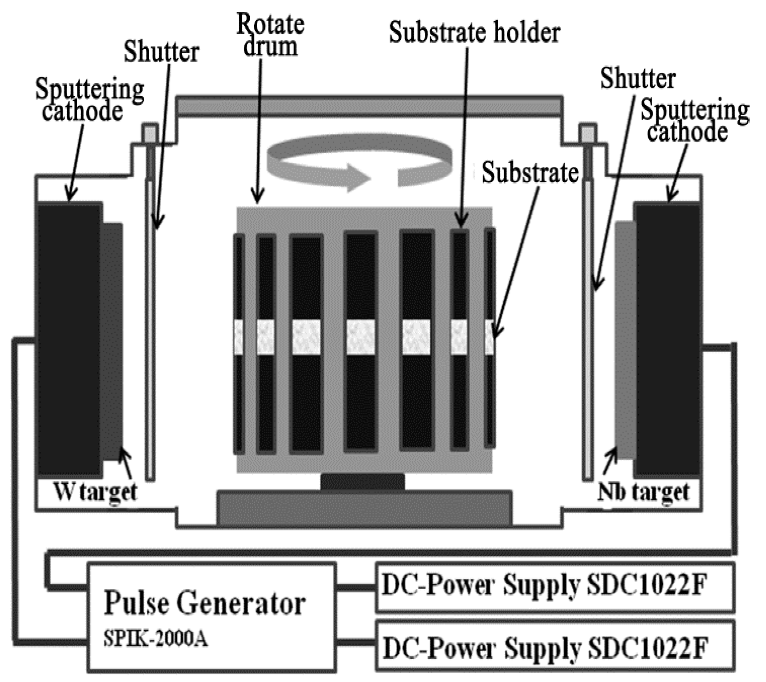
2.1. Film Deposition Process

WO3–Nb2O5 films were prepared by a home-made fast-alternative bipolar-pulsed reactive magnetron sputtering deposition system, as shown in Figure 1. The vacuum chamber was evacuated by a rotary pump and turbo-molecular pump. The substrates were affixed to vertical mounting plates and were placed on a cylindrical drum which rotated at 60 rpm (revolutions per minute) during deposition. The tungsten (W) and niobium (Nb) targets were also mounted vertically and placed face-to-face on opposite sides of the rotating drum, 70 mm away from the substrate. Both targets were 182 mm × 62 mm × 6 mm in size with a purity of 99.995%. The base pressure was 8.0 × 10⁻⁶ torr. Argon (Ar) was utilized as the sputtering gas with a flow rate of 50 sccm. The reactive gas was oxygen (O2), and, in this study, its flow rate was a variable parameter related to the discharge voltage. The total working pressure of Ar and O2 during deposition was maintained at 10 × 10−3 torr by using an auto-tuning throttle valve. The fast-alternating bipolar-pulsed reactive magnetron sputtering process was driven by two direct-current (DC) supplies (SDC-1022FDC, PSPLASMA Co., Seoul, South Korea) connected with a pulse controller (SPIK 2000A, Shen Chang Electric Co., Taipei, Taiwan). The pulse controller had an asymmetric pulse mode that allowed the sputtering power and pulse profile to be independently regulated for two sputtering targets, allowing more stability and control over the sputtering process and the proportion of pure WO3 and Nb2O5. All the experiments related to film deposition were carried out without substrate heating.
Indium tin oxide (ITO), WO3, WO3–Nb2O5, and Nb2O5 films were deposited on B270 Schott glass. The process parameters are listed in Table 1. Transparent electrodes of ITO film were deposited by DC reactive magnetron sputtering. All electrochromic films were deposited on the ITO in a single run. The oxygen flow rate for ITO film deposition was 1 sccm. Hall measurements for the sheet resistance, carrier concentration and mobility of the ITO film were carried out with an ACCENT HL5500 using the van der Pauw method. The sample size was 1 cm × 1 cm. The sheet resistance, carrier concentration and mobility of the ITO films were 29.5 Ω/□, 30.2 cm2·V−1·s−1 and 2.9 × 1020 cm−3, respectively. The WO3 and Nb2O5 films were deposited by DC reactive magnetron sputtering. The variously proportioned WO3–Nb2O5 films were deposited by fast-alternating bipolar-pulsed reactive dual magnetron sputtering under different sputtering powers. The sample results for W-Nb-150w, W-Nb-250w, W-Nb-350w, and W-Nb-450w, are shown in Table 1 and correspond to the different sputtering powers (from the Nb target) at 150, 250, 350 and 450 W, respectively. The bipolar pulse-width was modulated to have an on cycle of 50 μs and then an off cycle for 5 μs. The discharge voltage for the films was controlled by a home-made proportional-integral-derivative (PID) controller to ensure that the set point of the discharge voltage stabilized at the transition mode.

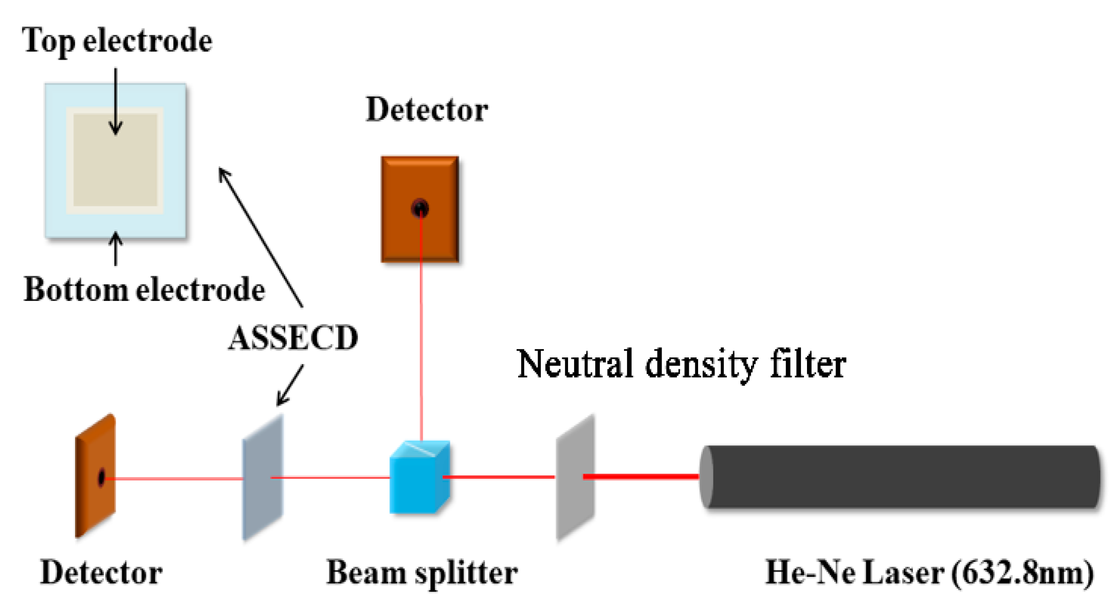
2.2. Film Characterizations

Scanning electron microscopy (SEM) images were taken on a Hitachi S-4800 scanning electron microscope (Hitachi, Tokyo, Japan) operated at an acceleration voltage of 10 kV. Energy dispersive X-ray spectroscopy analysis was performed on a Horiba EMAX-400 energy dispersive X-ray (EDX) (Horiba, Kyoto, Japan) microanalysis. The analytical conditions for EDX were as follows: accelerating voltage of 15 kV, working distance of 13.6 mm and magnification of 3000×. The samples were Pt coated to eliminate charging effects. The thin film crystalline structures were examined by X-ray diffraction (XRD) measurements carried out on a Bruker D8A using CuKα radiation (Bruker, Billerica, MA, USA) (λ = 0.154060 nm) operated with glancing angle (an incident angle of 1°) θ/2θ measurements of 20°–70°. The transmittance curves for the colored and bleached WO3, WO3–Nb2O5, and Nb2O5 electrochromic films were measured using a Perkin-Elmer Lambda-900 optical spectrophotometer (Waltham, MA, USA) in the 350–2000 nm wavelength range. The refractive index, n, extinction coefficient, k, and film thickness of the WO3, WO3–Nb2O5, and Nb2O5 films were calculated at different positions using the envelope method [30].
The electrochemical properties of the WO3, WO3–Nb2O5, and Nb2O5 electrochromic films were measured by a JIEHAN ECW-5000 (Jiehan Co., Taichung, Taiwan). Cyclic voltammetry (CV) and chronoamperometric (CA) experiments were performed in a three-electrode arrangement. Platinum (Pt) sheets were used as the counter electrode, saturated calomel electrode (SCE) as the reference-electrode in the cell with an electrochromic film/ITO/glass substrate as the working electrode in a liquid electrolyte consisting of 1 M lithium perchlorate (LiClO4) dissolved in propylene carbonate (PC). CV was carried out for 10 cycles using a saw-tooth wave signal ranging from ±1.0 V at a scan rate of 20 mV/s. The CA voltage switched between ±1.0 V (square wave) every 60 s (120 s/cycle) for 175 cycles.

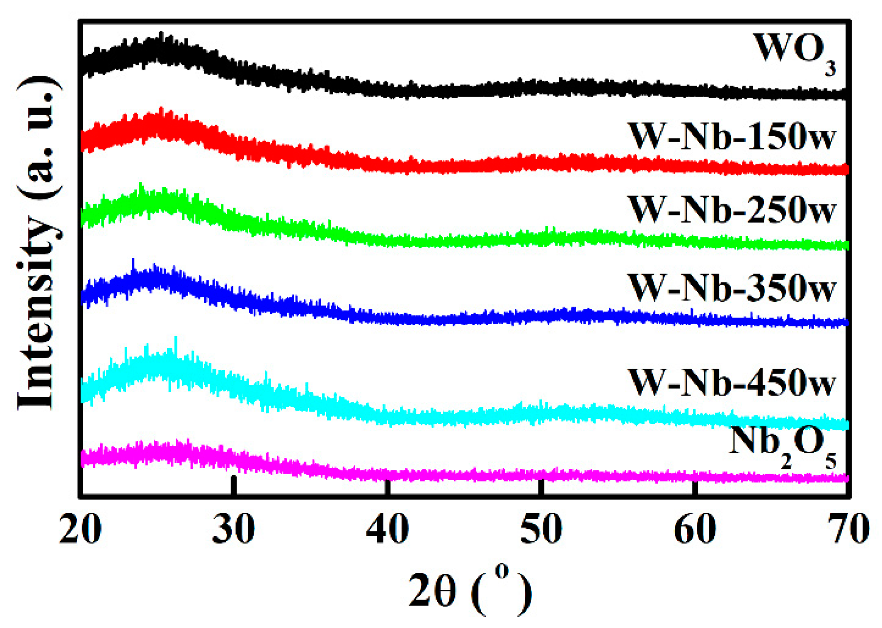
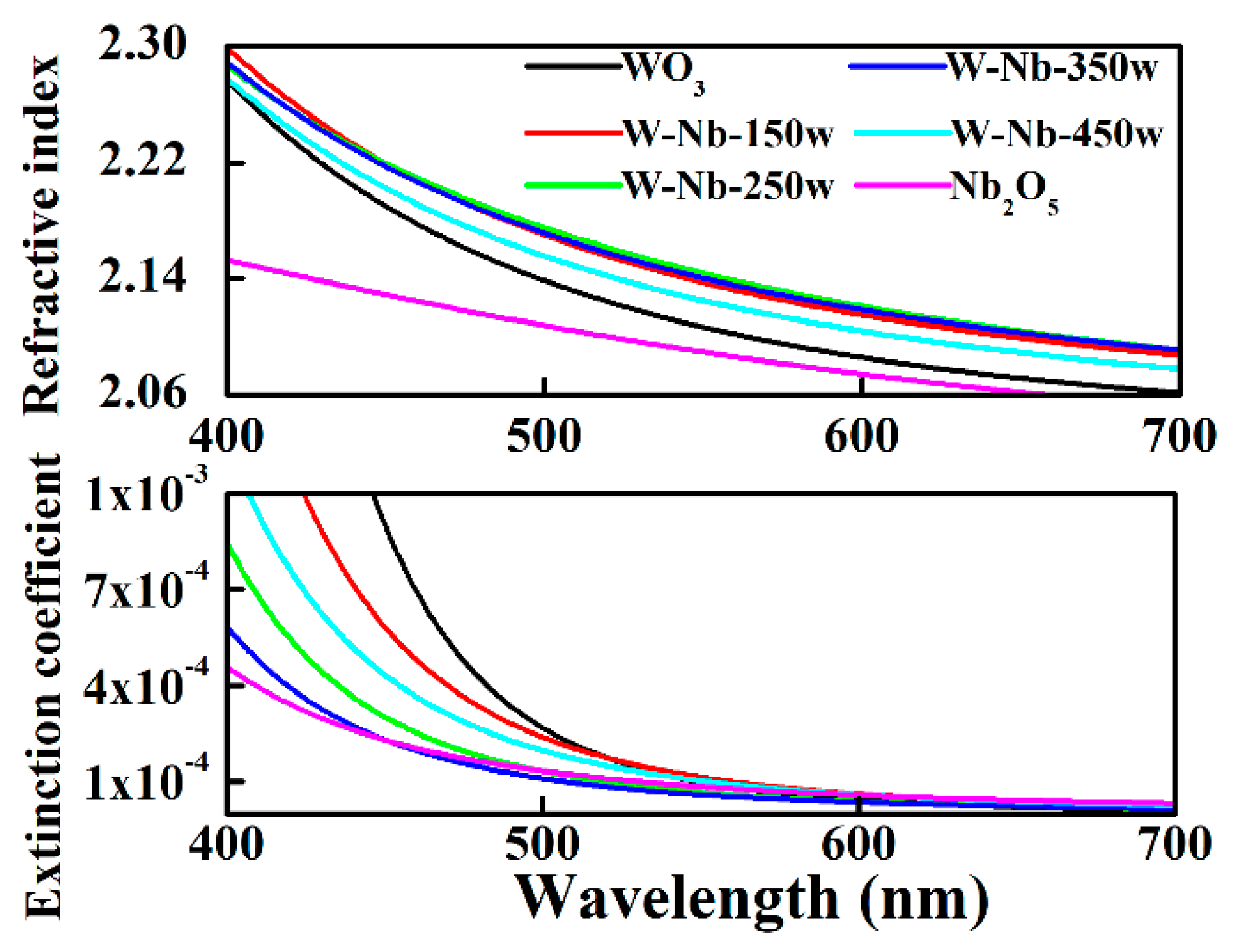
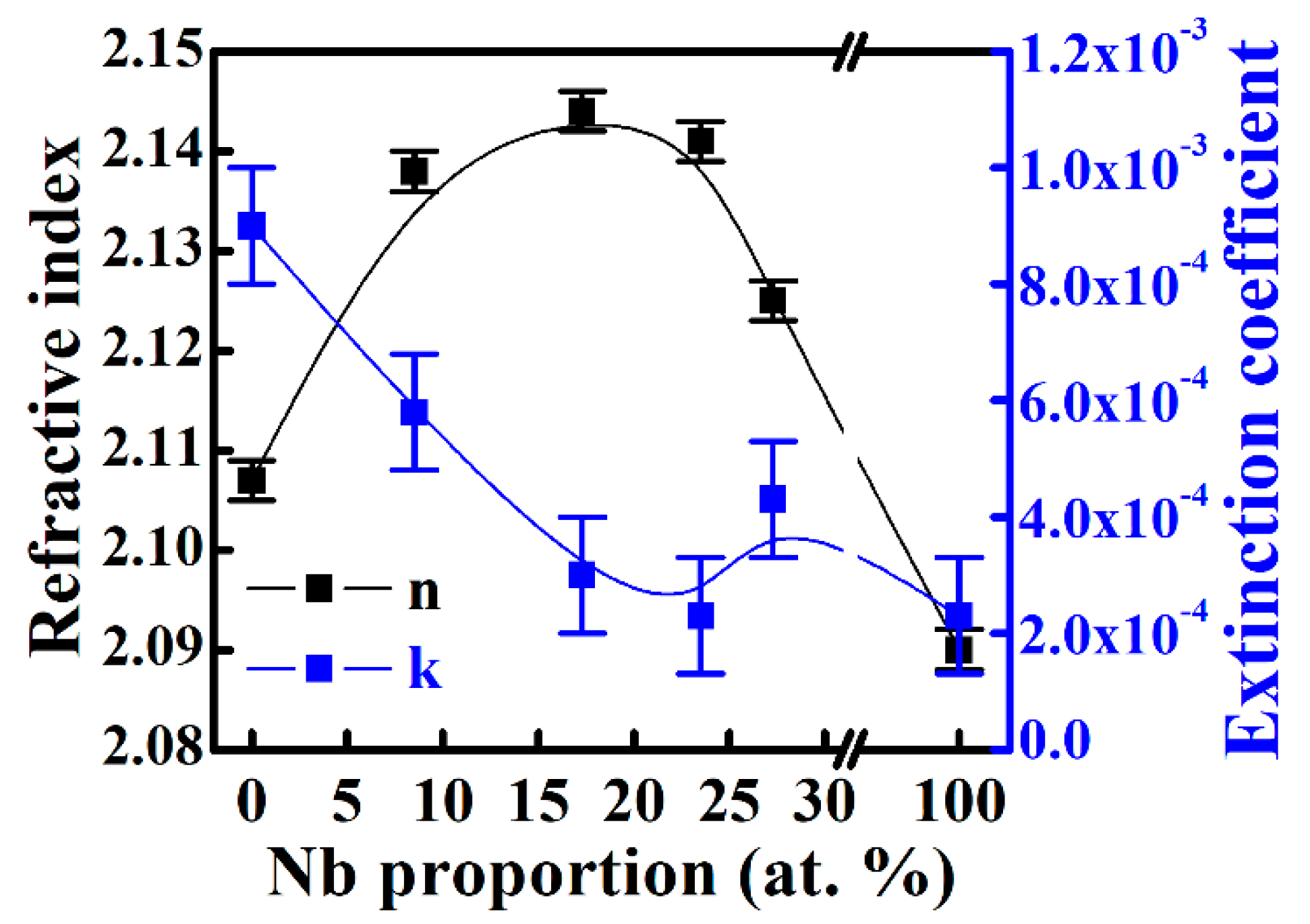
3. Results and Discussion

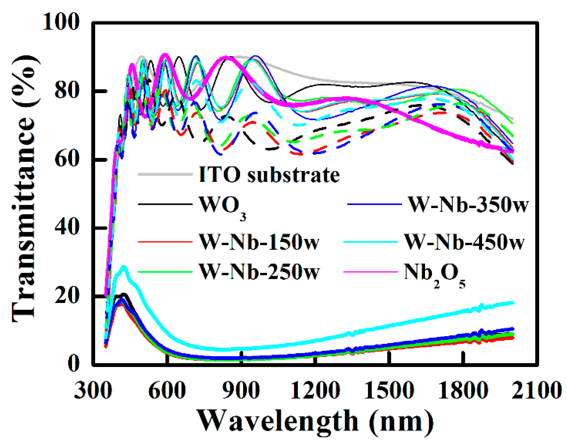
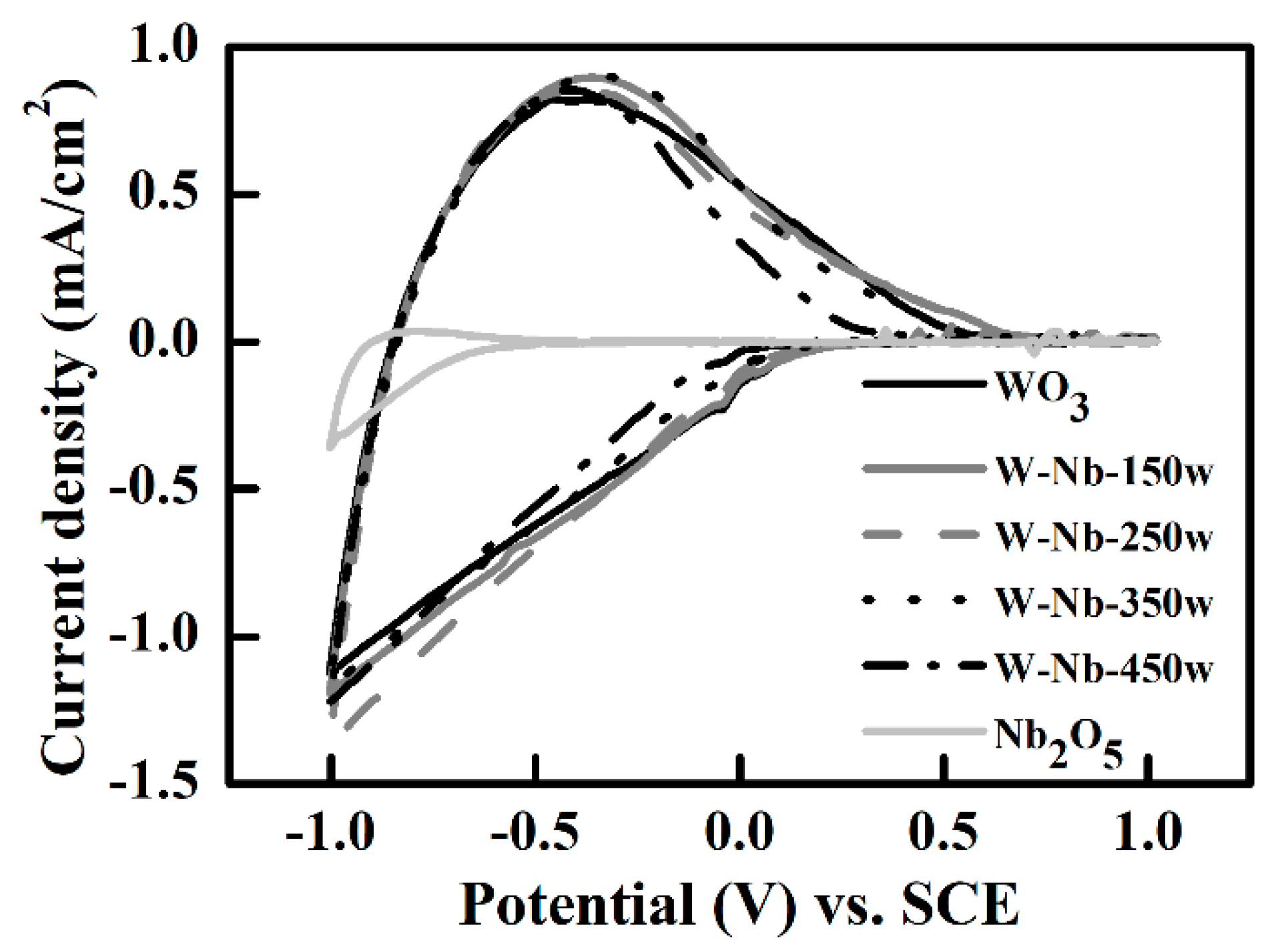
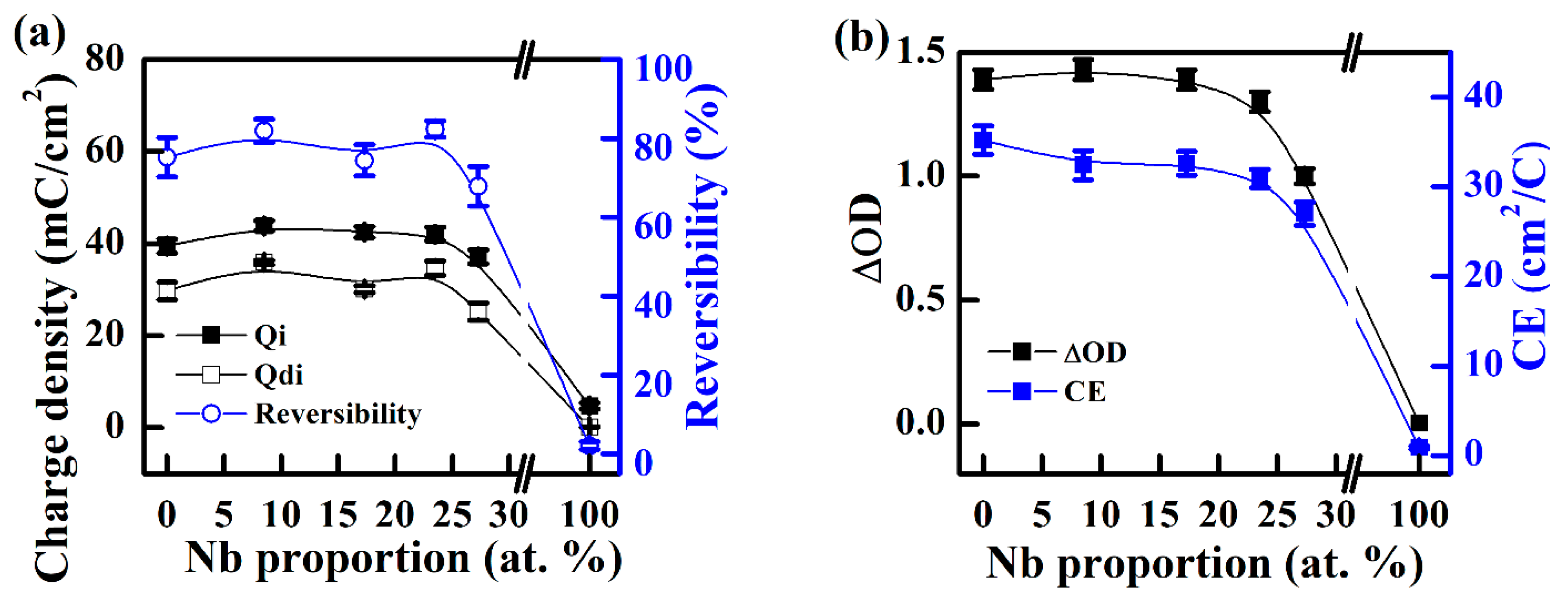
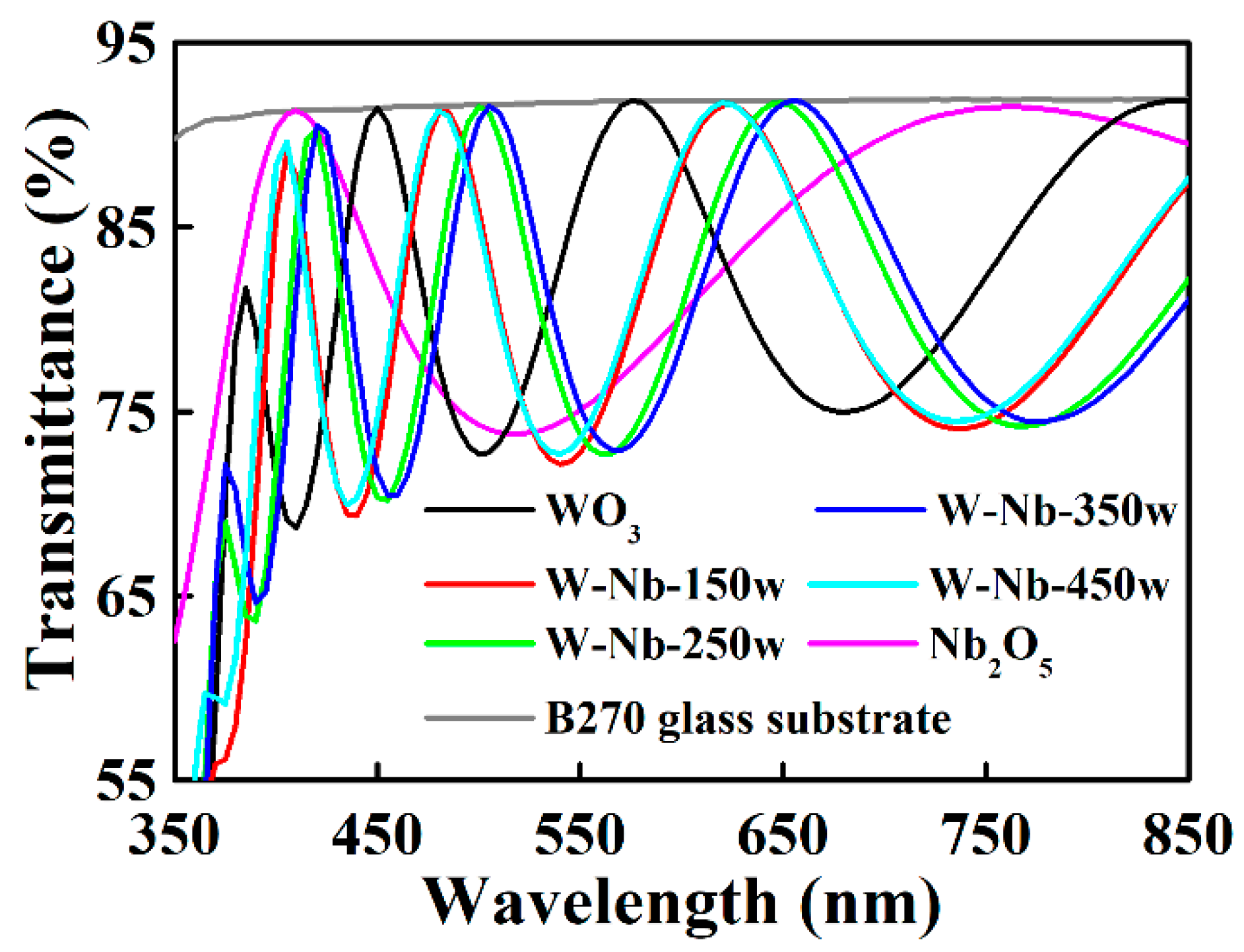
3.1. Electrochromic Films

Figure 2 shows the composition of films with different sputtering powers on the Nb target. The Nb proportions of the W-Nb-150w, W-Nb-250w, W-Nb-350w, and W-Nb-450w films were 8.5%, 17.3%, 23.5% and 27.3%. This indicated that the proportion of Nb2O5 in the WO3–Nb2O5 composite films increases with the increase in the sputtering power on the Nb target. SEM morphology evolutions of the W-Nb-150w, W-Nb-250w, W-Nb-350w, W-Nb-450w, and Nb2O5 films are shown in Figure 2. The surface structures of the as-deposited films of WO3, W-Nb-150w, W-Nb-250w, W-Nb-350w, and W-Nb-450w showed uniformly distributed spherical-shaped grains and compactly packed grains distributed over the film surface, and no evidence was found for any significant relationship of the WO3–Nb2O5 composite films between the surface structure and Nb2O5 content. Figure 3f shows the morphology of Nb2O5 film that has a larger grain size than pure WO3 film and WO3–Nb2O5 composite films. The XRD patterns of deposited films are shown in Figure 4. The pure WO3 film, WO3–Nb2O5 composite films and pure Nb2O5 film were amorphous films.
The optical transmittance spectra for the WO3, WO3–Nb2O5, and Nb2O5 films deposited on B270 glass substrates are shown in Figure 5. These films were homogeneous and had weak absorptions. The refractive indices, n, and extinction coefficients, k, of the WO3, WO3–Nb2O5, and Nb2O5 films are shown in Figure 6. The refractive indices at 550 nm and extinction coefficients at 450 nm of the WO3, W-Nb-150w, W-Nb-250w, W-Nb-350w, W-Nb-450w, and Nb2O5 films are shown in Figure 7. The optical constant of WO3 films depends on deposition conditions (e.g., deposition method, sputtering pressure, substrate temperature, etc.). However, few researchers have discussed the optical constants of WO3 films. The refractive index and extinction coefficient of WO3 films were in the range of 1.9–2.1 and 1 × 10⁻³–4 × 10⁻², respectively. The experimentally determined refractive index and extinction coefficient were in good agreement with the reported literature values for WO3 films [31,32,33,34,35]. Little literature has reported the optical constants of Nb2O5-doped WO3 films. In this study, the refractive indices of the WO3–Nb2O5 composite films were higher than those of the pure WO3 and Nb2O5 films, with the refractive index of composite films being highest when the sputtering power on the Nb target was 250 W. This resulted in a dense film with WO3 being mixed with Nb2O5 [31,32,33,35]. The extinction coefficient of the WO3–Nb2O5 films was between that of pure WO3 and Nb2O5 films. The extinction coefficient of all films was smaller than 1 × 10⁻³. The low value of extinction coefficients indicated nearly stoichiometric films. The WO3–Nb2O5 composite films produced with a sputtering power (from the Nb target) of 350 W and pure Nb2O5 film had lower extinction coefficient values than the other composite films.
The results for the dependence of the optical transmittance on the wavelength in the range of 400–2000 nm for pure WO3, Nb2O5, and WO3–Nb2O5 composite films in the as-deposited, bleached and colored states are shown in Figure 8. After the film was deposited on an ITO glass substrate, the sample was removed from the deposition chamber and immediately immersed in a liquid electrolyte. This sample as a working electrode, a Pt sheet as a counter-electrode and a SCE as a reference-electrode were immersed in a liquid electrolyte consisting of 1 M LiClO4 in PC. A DC voltage of −1 V was applied for 60 s between the two electrodes to inject Li+ ions into the sample. The sample was taken from the liquid electrolyte, and the LiClO4 solute and PC solvent were removed from the surface of the sample by blowing nitrogen, and the sample was placed in a spectrometer to measure the transmittance. The transmittances at wavelength of 633 nm for the WO3, W-Nb-150w, W-Nb-250w, W-Nb-350w, W-Nb-450w, and Nb2O5 films deposited on ITO glass substrates were respectively, about 88.9%, 79.1%, 75.8%, 74.9%, 78.2%, and 84.1% for the as-deposited films, 78.8%, 69.5%, 68.7%, 68.5%, 74.7%, and 84.5% for the bleached state films, and 3.2%, 2.6%, 2.8%, 3.5%, 7.4%, and 83.7% for the colored state films. Thus, the transmission modulations (ΔT) of the WO3, W-Nb-150w, W-Nb-250w, W-Nb-350w, W-Nb-450w, and Nb2O5 films were 75.5%, 66.8%, 65.9%, 65.0%, 67.3%, and 0.8%, respectively, indicating a decrease in the value of ΔT in the Nb2O5-doped WO3 films for all Nb2O5 doped concentration studied. It was noted that the transmittances of the pure WO3 films and WO3–Nb2O5 composite films in the bleached state were lower than for the as-deposited samples. When pure WO3 films and WO3–Nb2O5 composite films were deposited with an excess of oxygen in the sputtering gas, the interstitial oxygen in the electrochromic films reacted with the Li+ ion during the Li+ ion intercalation process to form a Li2O compound [36,37]. Thus, a fraction of Li+ intercalation was colored but not bleached again.
The change in the optical density (ΔOD) at a wavelength of 633 nm between samples in the bleached and colored states was calculated as follows:
( Δ OD ) 633 nm = log ( T b T c )
where Tb and Tc are the transmittances at a wavelength 633 nm of the bleached and colored states, respectively. The ΔOD of the WO3, W-Nb-150w, W-Nb-250w, W-Nb-350w, W-Nb-450w, and Nb2O5 films were 1.39, 1.43, 1.39, 1.29, 1.00, and 0.00, respectively. The changes in optical density of the WO3–Nb2O5 composite films were similar to that of the pure WO3 film as the sputtering power on the Nb target was lower than 350 W (Nb proportion less than 23.5%). The change in optical density decreased as the sputtering power on the Nb target was higher than 350 W (Nb proportion more than 23.5%). Furthermore, the transmission modulation and change in optical density of the pure Nb2O5 film did not change with the Li+ ion intercalation/deintercalation. In general, the TT-Nb2O5 film has high electrochromic properties [38]. In this study, the results show that the structure of pure Nb2O5 film is amorphous, with no electrochromic ability.
The cyclic voltammograms (CV) recorded for the WO3, WO3–Nb2O5 and Nb2O5 films are shown in Figure 9. The anodic peak current densities for the WO3, W-Nb-150w, W-Nb-250w, W-Nb-350w, W-Nb-450w, and Nb2O5 films were around 0.819, 0.898, 0.847, 0.902, 0.854, and 0.037 mA/cm2, respectively. There was a significant drop off in the ionic mobility of the WO3, W-Nb-150w, W-Nb-250w, W-Nb-350w, W-Nb-450w, and Nb2O5 films at −0.383, −0.363, −0.403, −0.343, −0.423, and −0.783 V, respectively. The CV curves for the WO3 and WO3–Nb2O5 films displayed a broad oxidation peak. Physically, this means that complete bleaching (maximum diffusion flux) was achieved at this point. There was no abrupt peak during the reduction (coloration) process, and the Li+ ion insertion/extraction was completely reversible. The cathodic peak current density of the WO3, W-Nb-150w, W-Nb-250w, W-Nb-350w, W-Nb-450w, and Nb2O5 films was completed at −1.124, −1.192, −1.357, −1.170, −1.219, and −0.359 mA/cm2, respectively. The cathodic peak current density increased, indicating that the Li+ ions could easily diffuse into the mixed WO3–Nb2O5 films. It is also mentioned in the literature [22] that the cathodic peak intensity is representative of the diffusion of ions and that following the anodic peak, the ionic mobility decreased, explaining the drop in current.
In comparison with mixed WO3–Nb2O5 films, as mentioned previously, the threshold voltage of the cathodic current shifts toward a more negative potential with a smaller current under the condition of pure Nb2O5 film. This result can be interpreted as a much higher charge transfer resistance occurring on the Nb2O5 film. Similar behavior also occurred in the various conditions of WO3–Nb2O5 films. Analyzing the cathodic region of CV curves in more detail, the resistance (slope of the IV curve) of the system is slightly higher under conditions with higher applied power (containing a higher percentage of Nb2O5). These results can be used to confirm the properties of Nb2O5 film, which is a media with good ionic conductivity for Li+ but also an insulator for electrons. In the anodic region of CV curves, there is hardly any current that occurs under the condition of pure Nb2O5 film. This phenomenon can also be explained by the characteristics of Nb2O5 film as follows. When the electrode with Nb2O5 films turned to an anode, the Li+ diffused away through the Nb2O5 films toward the new cathode, and the electrons in the electrolyte migrated toward the anode, synchronously. However, the electrons hardly transferred through the Nb2O5 film.
Figure 10 shows the chronoamperometry (CA) data recorded for the WO3, WO3–Nb2O5, and Nb2O5 films. The lifetime is defined as the number of cycles corresponding to a 30% decrease of the initial cathodic peak current density. The number of cycles of the WO3, W-Nb-150w, and W-Nb-250w films was about 43, 85 and 150, respectively. When the sputtering power on the Nb target was higher than 250 W (Nb proportion higher than 17.3%), the lifetime of the WO3–Nb2O5 films was surpassed 178 cycles, that is, they were 4 times longer than that of pure WO3 films. Although there was a decrease in the current for the WO3 and Nb2O5 films with increased cycles, the current of the WO3–Nb2O5 films changed less with respect to the number of cycles, indicating that the WO3–Nb2O5 films are more stable, and thus, more durable.
In this study, Nb2O5 was used as an ion-conductor in the Nb2O5-doped WO3 films. The coloration efficiency (CE) and reversibility (R) were calculated by using the following expressions:
CE = ( Δ OD ) 633 nm Q i
R ( % ) = Q i Q d i × 100 %
where Qi and Qdi are the amount of charge intercalated and deintercalated, respectively. The reversibility of the films was calculated as a ratio of charge deintercalated to charge intercalated in the film. The reversibility values for the WO3, W-Nb-150w, W-Nb-250w, W-Nb-350w, W-Nb-450w, and Nb2O5 films were 75.3%, 82.0%, 74.5%, 82.4%, 67.9%, and 2.1%, respectively. The reversibility ranged from about 74.5% to 82.4% as the sputtering power on Nb target of 0–350 W (Nb fraction ranged from 0% to 23.5%), and the reversibility was decreased from 82.4% to 2.1% as the sputtering power on the Nb target was higher than 350W (Nb fraction higher than 23.5%). The intercalated and deintercalated charge density and reversibility are shown in Figure 11a. The CE values for the WO3, W-Nb-150w, W-Nb-250w, W-Nb-350w, W-Nb-450w, and Nb2O5 films were 35.2, 32.4, 32.6, 30.9, 27.0, and 0.9 cm2/C, respectively, indicating a slight decrease in the value of CE in the Nb2O5-doped WO3 films when the Nb2O5 doping concentration increased. ΔOD and CE for the WO3, WO3–Nb2O5, and Nb2O5 films at 633 nm are shown in Figure 11b. The CE values are in good agreement with the reported literature values for WO3 and WO3–Nb2O5 electrochromic films [2,5,22,23,39].

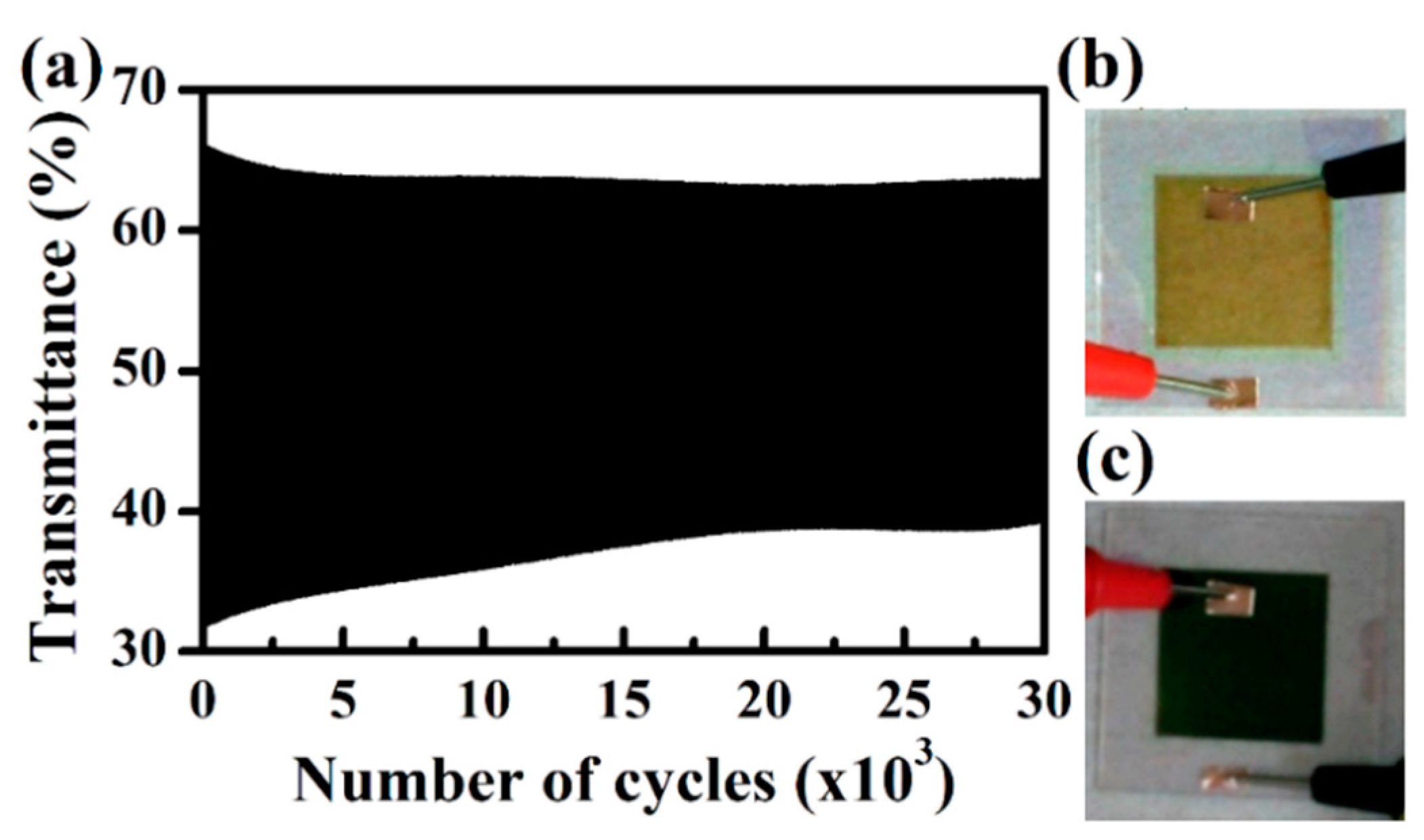
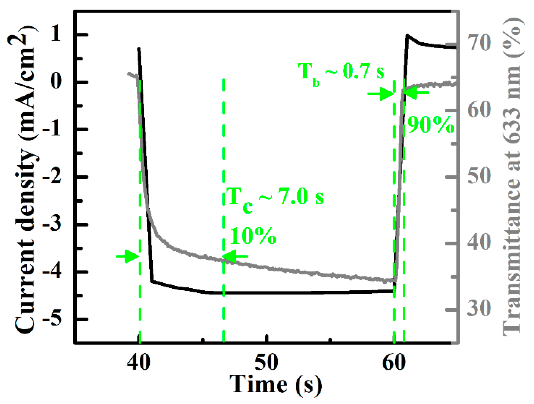
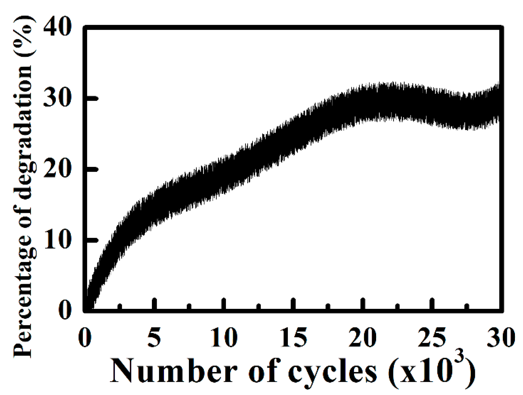
3.2. All-Solid-State Electrochromic Devices

A thin film ASSECD with a five layered structure of glass/ITO/ WO3–Nb2O5/Nb2O5/NiVOx/ITO was fabricated in this study, as shown in Figure 12. The WO3–Nb2O5 film corresponding to 350 W target sputtering power (Nb proportion as 23.5%) was used as an electrochromic layer, NiVOx as an ion storage layer and Nb2O5 as an ion conduction layer. Each layer was deposited in their respective conditions, as listed in Table 2. After the Nb2O5 film was deposited on a WO3–Nb2O5/ITO/glass substrate, the sample was removed from the deposition chamber and immediately immersed in a liquid electrolyte consisting of a 1 M solution of LiClO4 dissolved in PC. This sample was used as a working electrode, a sheet of Pt was used as a counter-electrode and a SCE was used as a reference-electrode. A DC voltage of −1 V was applied for 60 s between the two electrodes to inject Li+ ions into the WO3–Nb2O5 film. A sample was taken from the liquid electrolyte, and a pressurized stream of nitrogen gas was used to remove the LiClO4 solute and PC solvent from the surface of the sample. After the Li+ impregnation process, the sample was then placed in the deposition chamber again to deposit the NiVOx and ITO films. A Ni (92 at.%)–V (8 at.%) alloy (non-magnetic) target 182 × 62 × 6 mm3 in size with a purity of 99.995% was used to deposit NiVOx films [29,40]. When the process of the device was complete, the samples were immediately measured using a homemade optical transmittance measurement system and JIEHAN ECW-5000 Electrochemical work station (Jiehan Co., Taichung, Taiwan) with a two-electrode cell configuration for transmission modulations, electrochromic performance, and durability, respectively. Conductive adhesive copper tape (3MTM Scotch 1181, 3M, Maplewood, MN, USA) was used at the top and bottom of the ITO electrodes to maintain an electrical contact. The optical transmittance (at 632.8 nm) for each specimen in a colored and bleached state was measured with a He–Ne laser source (MELLES GRIOT 25-LHP-828-249) and two photo-detectors (Silicon PIN Detector ET-2030 from EOT), as shown in Figure 13. Figure 14 and Figure 15 show the optical transmittance and current density of the ASSECD during repeated coloring and bleaching for 3 × 10⁴ cycles. The bleached and colored state photographs of the ASSECD after 3 × 10⁴ cycles are shown in Figure 14b,c, respectively. The applied voltage to the ASSECD was operated from 0 to −3 V, respectively, for coloring, and 0–3 V, respectively, for bleaching. The time for each coloration and bleaching cycle was fixed at 40 s. For the first cycle, the optical transmittances for the colored and bleached state were 33% and 66%, respectively, corresponding to a ΔT of 33%. After 3 × 10⁴ cycles, the optical transmittances for the colored and the bleached states changed to 40% and 63%, respectively, corresponding to a ΔT of 23%. Correspondingly, the initial current density for coloring and bleaching was −4.13 and 0.91 mA/cm2, respectively, during the first cycle, and then it decreased to −2.30 and 0.86 mA/cm2, respectively. The percentage of degradation is shown in Figure 16. The percentage of degradation was calculated by using Equation (4), where ΔT0 is the initial transmittance modulation before degradation and ΔTN is the transmittance modulation at each cycle. The ASSECD shows a percentage of degradation of around 30% after 30,000 cycles.
D ( % ) = Δ T 0 Δ T N Δ T 0 × 100 %
Figure 17 shows the current density and optical transmittance, coloring response time and bleaching response time for the second coloration and bleaching cycle. The response times during the coloring and bleaching processes were also quantitatively calculated from the transmittance curves. Here, the response time for the coloration and bleaching of ASSECD was defined as the time interval for the value to reach 90% and 10% of the final and initial transmittance values [27,28], according to the transmittance curves in Figure 17. The response times of the coloration and bleaching processes were about 7.0 and 0.7 s, respectively. The optical transmittance and current density decreased when the cycles of coloration and bleaching increased. That might be due to the Li+ ion being trapped by excess oxygen from the sputtering process and incorporated as interstitials in the structure of the film and moisture from an ambient environment penetrating through the device or residual water molecules being adsorbed during film preparation. Moisture causes irreversible electrochemical reactions which immobilize the lithium ion, subsequently reducing the device’s performance [14].

4. Conclusions

A fast-alternating bipolar-pulsed reactive magnetron sputtering deposition system was used to produce WO3–Nb2O5 electrochromic composite films and an ITO/WO3–Nb2O5/Nb2O5/NiVOx/ITO ASSECD. The sputtering power for the Nb targets was controlled in order to produce different compositions of WO3–Nb2O5 films. The pulse-width modulation of the W and Nb targets were programmed to be on for 50 μs and off for 5 μs, to produce WO3–Nb2O5 films.
The resulting WO3, WO3–Nb2O5 and Nb2O5 films were homogeneous and had a weak absorption. The mixed WO3–Nb2O5 composite films were dense, and their extinction coefficients were mostly between those of pure WO3 and Nb2O5 films. Interestingly, the WO3–Nb2O5 composite films produced with sputtering powers (on the Nb target) of 250 and 350 W, had the highest refractive index and lowest extinction coefficient values, respectively, for wavelengths longer than 450 nm.
By increasing the sputtering power on the Nb target from 150 to 350 W, the change of optical density and coloration efficiency slightly decreased from 1.43 to 1.29, and from 32.4 to 30.9 cm2/C, respectively. The change in optical density and coloration efficiency rapidly decreased with the sputtering power on the Nb target of 450 W. By mixing Nb2O5 with WO3, the reversibility improved and the durability increased. For example, for WO3–Nb2O5 film with sputtered power on the Nb target of 350 W (Nb proportion of 23.5%), the lifetime and reversibility exceeded 178 cycles and 82.4%, respectively, compared with 43 cycles and 75.3% for pure WO3 film. The transmission modulations of ASSECD based on a WO3–Nb2O5 film with sputtering power on the Nb target of 350 W (Nb proportion as 23.5%) construction was about 33% for initial cycles and 23% for 3 × 10⁴ cycles of coloring and bleaching. The device showed good performance with 30% degradation after 3 × 10⁴ cycles. The response times for coloration and bleaching were about 7.0 and 0.7 s, respectively. As such, this work indicates that the electrochromic properties, such as the operating lifetime and response time, of the WO3–Nb2O5 composite films are better than those of pure WO3 films, which suggests a strong potential for future applications in electrochromic devices.

Author Contributions

Conceptualization, C.-J.T.; Methodology, C.-J.T. and J.-L.H.; Formal Analysis, C.-J.T. and C.-H.C.; Investigation, C.-J.T.; Resources, C.-C.J.; Data Curation, C.-J.T.; Writing-Original Draft Preparation, C.-L.T., C.-C.J., C.-J.L. and C.-Y.H.; Writing-Review & Editing, C.-J.T. and C.-L.T.; Project Administration, C.-J.T.; Funding Acquisition, C.-J.T. and C.-L.T.

Funding

This research was funded by Ministry of Science and Technology of Taiwan (Nos. MOST 101-2221-E-159-016, MOST 106-2221-E-035-073 and MOST 106-2221-E-035-072-MY2).

Acknowledgments

Authors are grateful for the Precision Instrument Support Center of Feng Chia University in providing materials analytical facilities.

Conflicts of Interest

The authors declare no conflict of interest.

References

  1. Granqvist, C.G.; Azens, A.; Isidorsson, J.; Kharrazi, M.; Kullman, L.; Lindstrtöm, T.; Niklasson, G.A.; Ribbing, C.G.; Rönnow, D.; Strømme Mattsson, M.; et al. Towards the smart window: Progress in electrochromics. J. Non-Cryst. Solids 1997, 218, 273–279. [Google Scholar] [CrossRef]
  2. Granqvist, C.G. Electrochromic tungsten oxide films: Review of progress 1993–1998. Sol. Energy Mater. Sol. Cells 2000, 60, 201–262. [Google Scholar] [CrossRef]
  3. Granqvist, C.G. Oxide electrochromics: Why, how, and whither. Sol. Energy Mater. Sol. Cells 2008, 92, 203–208. [Google Scholar] [CrossRef]
  4. Papaefthimiou, S.; Syrrakou, E.; Yianoulis, P. An alternative approach for the energy and environmental rating of advanced glazing: An electrochromic window case study. Energy Build. 2009, 41, 17–26. [Google Scholar] [CrossRef]
  5. Vernardou, D.; Psifis, K.; Louloudakis, D.; Papadimitropoulos, G.; Davazoglou, D.; Katsarakis, N.; Koudoumas, E. Low pressure CVD of electrochromic WO3 at 400 °C. J. Electrochem. Soc. 2015, 162, H579–H582. [Google Scholar] [CrossRef]
  6. Louloudakis, D.; Vernardou, D.; Papadimitropoulos, G.; Davazoglou, D.; Koudoumas, E. The effect of growth time and oxygen on the properties of electrochromic WO3 thin layers grown by LPCVD. Adv. Mater. Lett. 2018, 9, 578–584. [Google Scholar] [CrossRef]
  7. Baucke, F.G. Electrochromic mirrors with variable reflectance. Sol. Energy Mater. 1987, 16, 67–77. [Google Scholar] [CrossRef]
  8. Bange, K.; Gambke, T. Electrochromic materials for optical switching devices. Adv. Mater. 1990, 2, 10–16. [Google Scholar] [CrossRef]
  9. Corr, D.; Bach, U.; Fay, D.; Kinsella, M.; McAtamney, C.; O’Reilly, F.; Rao, S.N.; Stobie, N. Coloured electrochromic “paper-quality” displays based on modified mesoporous electrodes. Solid State Ionics 2003, 165, 315–321. [Google Scholar] [CrossRef]
  10. Vlachopoulos, N.; Nissfolk, J.; Möller, M.; Briançon, A.; Corr, D.; Grave, C.; Leyland, N.; Mesmer, R.; Pichot, F.; Ryan, M.; et al. Electrochemical aspects of display technology based on nanostructured titanium dioxide with attached viologen chromophores. Electrochim. Acta 2008, 53, 4065–4071. [Google Scholar] [CrossRef]
  11. Argun, A.A.; Reynolds, J.R. Line patterning for flexible and laterally configured electrochromic devices. J. Mater. Chem. 2005, 15, 1793–1800. [Google Scholar] [CrossRef]
  12. Schlotter, P.; Pickelmann, L. The xerogel structure of thermally evaporated tungsten oxide layers. J. Electron. Mater. 1982, 11, 207–236. [Google Scholar] [CrossRef]
  13. Shiyanovskaya, I.V. Structure rearrangement and electrochromic properties of amorphous tungsten trioxide films. J. Non-Cryst. Solids 1995, 187, 420–424. [Google Scholar] [CrossRef]
  14. Tajima, K.; Hotta, H.; Yamada, Y.; Okada, M.; Yoshimura, K. Degradation studies of electrochromic all-solid-state switchable mirror glass under various constant temperature and relative humidity conditions. Sol. Energy Mater. Sol. Cells 2010, 94, 2411–2415. [Google Scholar] [CrossRef]
  15. Hashimoto, S.; Matsuoka, H. Lifetime of electrochromism of amorphous WO3-TiO2 thin films. J. Electrochem. Soc. 1991, 138, 2403–2408. [Google Scholar] [CrossRef]
  16. Ozer, N.; Lampert, C.M. Electrochromic performance of sol-gel deposited WO3-V2O5 films. Thin Solid Films 1999, 349, 205–211. [Google Scholar] [CrossRef]
  17. Da Costa, E.; Avellaneda, C.O.; Pawlicka, A. Alternative Nb2O5-TiO2 thin films for electrochromic devices. J. Mater. Sci. 2001, 36, 1407–1410. [Google Scholar] [CrossRef]
  18. Rougier, A.; Blyr, A.; Garcia, J.; Zhang, Q.; Impey, S.A. Electrochromic W–M–O (M = V, Nb) sol-gel thin films: A way to neutral colour. Sol. Energy Mater. Sol. Cells 2002, 71, 343–357. [Google Scholar] [CrossRef]
  19. Ivanova, T.; Gesheva, K.A.; Kalitzova, M.; Marsen, B.; Cole, B.; Miller, E.L. Electrochromic behavior of Mo/W oxides related to their surface morphology and intercalation process parameters. Mater. Sci. Eng. B 2007, 142, 126–134. [Google Scholar] [CrossRef]
  20. Arvizu, M.A.; Triana, C.A.; Stefanov, B.I.; Granqvust, C.G.; Niklasson, G.A. Electrochromism in sputtering-deposited W–Ti oxide films: Durability enhancement due to Ti. Sol. Energy Mater. Sol. Cells 2014, 125, 184–189. [Google Scholar] [CrossRef]
  21. Pehlivan, E.; Tepehan, F.Z.; Tepehan, G.G. Comparison of optical, structural and electrochromic properties of undoped and WO3-doped Nb2O5 thin films. Solid State Ionics 2003, 165, 105–110. [Google Scholar] [CrossRef]
  22. Bathe, S.R.; Patil, P.S. Influence of Nb doping on the electrochromic properties of WO3 films. J. Phys. D Appl. Phys. 2007, 40, 7423–7431. [Google Scholar] [CrossRef]
  23. Wang, C.K.; Sahu, D.; Wang, S.C.; Huang, J.L. Electrochromic Nb-doped WO3 films: Effects of post annealing. Ceram. Int. 2012, 38, 2829–2833. [Google Scholar] [CrossRef]
  24. Zhang, X.; Zhang, H.; Li, Q.; Luo, H. An all-solid-state inorganic electrochromic display of WO3 and NiO film with LiNbO3 ion conductor. IEEE Electron Device Lett. 2000, 21, 215–217. [Google Scholar] [CrossRef]
  25. Atak, G.; Coşkun, Ö. LiNbO3 thin film for all-solid-state electrochromic devices. Opt. Mater. 2018, 81, 160–167. [Google Scholar] [CrossRef]
  26. Coşkun, Ö.D.; Atak, G. The effects of lithiation process on the performance of all-solid-state electrochromic devices. Thin Solid Films 2018, 662, 13–20. [Google Scholar] [CrossRef]
  27. Liu, Q.; Dong, G.; Xiao, Y.; Gao, F.; Wang, M.; Wang, Q.; Wang, S.; Zuo, H.; Diao, X. An all-thin-film inorganic electrochromic device monolithically fabricated on flexible PET/ITO substrate by magnetron sputtering. Mater. Lett. 2015, 142, 232–234. [Google Scholar] [CrossRef]
  28. Liu, Q.; Dong, G.; Chen, Q.; Guo, J.; Xiao, Y.; Delplancke-Ogletree, M.P.; Reniers, F.; Diao, X. Charge-transfer kinetics and cyclic properties of inorganic all-solid-state electrochromic device with remarkably improve optical memory. Sol. Energy Mater. Sol. Cells 2018, 174, 545–553. [Google Scholar] [CrossRef]
  29. Tang, C.-J.; Ye, J.-M.; Yang, Y.-T.; He, J.-L. Large-area flexible monolithic ITO/WO3/Nb2O5/NiVOx/ITO electrochromic devices prepared by using magnetron sputter deposition. Opt. Mater. 2016, 55, 83–89. [Google Scholar] [CrossRef]
  30. Manifacier, J.C.; Gasiot, J.; Fillard, J.P. A simple method for the determination of the optical constants n, k and the thickness of the weakly absorbing thin film. J. Phys. E Sci. Instrum. 1976, 9, 1002. [Google Scholar] [CrossRef]
  31. Özkan, E.; Tepehan, F.Z. Optical and structural characteristics of sol-gel-deposited tungsten oxide and vanadium-doped tungsten oxide films. Sol. Energy Mater. Sol. Cells 2001, 68, 265–277. [Google Scholar] [CrossRef]
  32. Washizu, E.; Yamamoto, A.; Abe, Y.; Kawamura, M.; Sasaki, K. Optical and electrochromic properties of RF reactively sputtered WO3 films. Solid State Ionics 2003, 165, 175–180. [Google Scholar] [CrossRef]
  33. Subrahmanyam, A.; Karuppasamy, A. Optical and electrochromic properties of oxygen sputtered tungsten oxide (WO3) thin films. Sol. Energy Mater. Sol. Cells 2007, 91, 266–274. [Google Scholar] [CrossRef]
  34. Karuppasamy, A.; Subrahmanyam, A. Studies on electrochromic smart windows based on titanium doped WO3 thin films. Thin Solid Films 2007, 516, 175–178. [Google Scholar] [CrossRef]
  35. Sun, X.; Liu, Z.; Cao, H. Effects of film density on electrochromic tungsten oxide thin films deposited by reactive dc-pulsed magnetron sputtering. J. Alloy. Compd. 2010, 504, S418–S421. [Google Scholar] [CrossRef]
  36. Niklasson, G.A.; Berggren, L.; Larsson, A.L. Electrochromic tungsten oxide: The role of defects. Sol. Energy Mater. Sol. Cells 2004, 84, 315–328. [Google Scholar] [CrossRef]
  37. Inamdar, A.I.; Kim, Y.S.; Jang, B.U.; Im, H.; Jung, W.; Kim, D.Y.; Kim, H. Effects of oxygen stoichiometry on electrochromic properties in amorphous tungsten oxide films. Thin Solid Films 2012, 520, 5367–5371. [Google Scholar] [CrossRef]
  38. Huang, Y.; Zhang, Y.; Hu, X. Structure, morphological and electrochromic properties of Nb2O5 films deposited by reactive sputtering. Sol. Energy Mater. Sol. Cells 2003, 77, 155–162. [Google Scholar] [CrossRef]
  39. Bathe, S.R.; Patil, P.S. Electrochromic characteristics of fibrous reticulated WO3 thin films prepared by pulsed spray pyrolysis technique. Sol. Energy Mater. Sol. Cells 2007, 91, 1097–1101. [Google Scholar] [CrossRef]
  40. Ye, J.-M.; Lin, Y.-P.; Yang, Y.-T.; Chang, J.-T.; He, J.-L. Electrochromic properties of Ni(V)Ox films deposited via reactive magnetron sputtering with a 8V–92Ni alloy target. Thin Solid Films 2010, 519, 1578–1582. [Google Scholar] [CrossRef]
Figure 1. Schematic representation of the fast-alternating asymmetric bipolar pulsed reactive dual magnetron sputtering deposition system.
Coatings 09 00009 g001
Figure 2. The proportions of niobium (Nb) versus different sputtering powers on Nb target.
Coatings 09 00009 g002
Figure 3. SEM morphologies for (a) WO3, (b) W-Nb-150w, (c) W-Nb-250w, (d) W-Nb-350w, (e) W-Nb-450w, and (f) Nb2O5 films.
Coatings 09 00009 g003
Figure 4. XRD patterns of WO3, WO3–Nb2O5, and Nb2O5 films.
Coatings 09 00009 g004
Figure 5. Transmittance spectra of WO3, WO3–Nb2O5, and Nb2O5 films coated on B270 glass substrates.
Coatings 09 00009 g005
Figure 6. Refractive index and extinction coefficient versus wavelength for WO3, WO3–Nb2O5, and Nb2O5 films.
Coatings 09 00009 g006
Figure 7. Refractive index at 550 nm and extinction coefficient at 450 nm for different niobium proportions.
Coatings 09 00009 g007
Figure 8. Spectra for the as-deposited (thin line), colored states (thick line) and bleached states (dashed line) of WO3, WO3–Nb2O5, and Nb2O5 films deposited on ITO coated B270 glass substrates.
Coatings 09 00009 g008
Figure 9. Cyclic voltammograms for WO3, WO3–Nb2O5, and Nb2O5 films.
Coatings 09 00009 g009
Figure 10. Chronoamperometry for WO3, WO3–Nb2O5, and Nb2O5 films.
Coatings 09 00009 g010
Figure 11. (a) Intercalated and deintercalated charge density and reversibility; (b) Optical density (ΔOD) and coloration efficiency (CE) for the WO3, W-Nb-150w, W-Nb-250w, W-Nb-350w, W-Nb-450w, and Nb2O5 films.
Coatings 09 00009 g011
Figure 12. Layered monolithic structure of the all-solid-state electrochromic device (ASSECD) constructed.
Coatings 09 00009 g012
Figure 13. Schematic optical transmittance measurement.
Coatings 09 00009 g013
Figure 14. (a) Optical transmittance of the ASSECD undergoing repeated coloring and bleaching for 3 × 10⁴ cycles; Photographs of the (b) bleached and (c) colored state of ASSECD after 3 × 10⁴ cycles.
Coatings 09 00009 g014
Figure 15. Current density of the ASSECD undergoing repeated coloring and bleaching for 3 × 10⁴ cycles.
Coatings 09 00009 g015
Figure 16. The percentage of degradation of ASSECD undergoing repeated coloring and bleaching for 3 × 10⁴ cycles.
Coatings 09 00009 g016
Figure 17. The response time for coloring (Tcolored) and bleaching (Tbleached) as determined from the transmittance of the ASSECD.
Coatings 09 00009 g017
Table 1. Process parameters (pressure, P; argon flux, fAr; oxygen flux, fO₂; sputtering power, Psp; discharge voltage, Vdischarge; film thickness, d) used for film deposition; indium tin oxide, ITO.
SamplesP (mtorr)fAr (sccm)fO₂ (sccm)Psp (W)Vdischarge (V)d (nm)
WO31050PID(DC)250550411
W-Nb-150w1050PID(Bipolar)W 250W 636442
Nb 150Nb 522
W-Nb-250w1050PID(Bipolar)W 250W 620462
Nb 250Nb 565
W-Nb-350w1050PID(Bipolar)W 250W 625467
Nb 350Nb 588
W-Nb-450w1050PID(Bipolar)W 250W 610443
Nb 450Nb 625
Nb2O51050PID(DC)500580186
ITO3401(DC)300355230
Table 2. Growth sequence and parameters used for all-solid-state electrochromic device.
Thin FilmP (mtorr)fAr (sccm)fO₂ (sccm)Psp (W)Vdischarge (V)d (nm)
ITO3401(DC)300355230
W-Nb-350w1050PID(Bipolar)W 250W 625350
Nb 350Nb 588
Nb2O51050PID(DC)500580230
NiVOx101256(DC)500400200
ITO3401(DC)300355230

