Microstructure and Mechanical Property Investigation of TaSiN Thin Films Deposited by Reactive Magnetron Sputtering


Department of Materials Science and Engineering, University of Texas at Arlington, Arlington, TX 76019, USA
*
Author to whom correspondence should be addressed.
Coatings 2019, 9(5), 338; https://doi.org/10.3390/coatings9050338
Submission received: 11 April 2019
/
Revised: 16 May 2019
/
Accepted: 23 May 2019
/
Published: 25 May 2019
(This article belongs to the Special Issue Mechanical Properties of Nanostructured Coatings)
Abstract
:Tantalum silicon nitride (Ta–Si–N) films were synthesized on Si substrate via magnetron sputtering. The structure and properties of the Ta–Si–N films were investigated as a function of the N2 content in the N2/Ar gas mixture. Increasing the N2 percentage in the gas mixture from 7% to 20% changed the film structure from textured hexagonal (hex) Ta2N to nontextured hex Ta2N to a mixture of face-centered cubic (fcc) TaN and hex Ta2N, and finally to fcc TaN. X-ray photoelectron spectroscopy showed Ta–N and Si–N bonds in the films. The film microstructure was found to change from columnar morphology with visible amorphous boundaries (at 13% N2) to columnar morphology with absence of amorphous boundaries (at 15% N2). Increasing N2 content increased hardness in the films with those deposited with 13–15% N2 displaying the highest hardness of ~40 ± 2 GPa. In addition, the 13% N2 films showed a ratio of H/E* > 0.11, elastic recovery of ~60%, low coefficient of friction of 0.6, reduced wear rate (7.09 × 10⁻⁶ mm3/N·m), and remained thermally stable up to 800 °C. The results suggest that the Ta–Si–N films have high potential as hard tribological nanocomposite coatings.
1. Introduction
Transition metal nitrides MeN (Me: transition metal) possess attractive physical, chemical, and mechanical properties that make them candidate materials for several engineering applications such as protective hard coatings, wear-resistant layers, diffusion barriers, and thin film resistors in microelectronics. Various Me-N systems, such as TiN, ZrN, CrN, etc. have been explored to some detail by researchers [1,2,3,4,5,6]. Of particular interest are the Nb-N and Ta-N systems since they exhibit several metastable and stable phases. For instance, Ta–N exhibits orthorhombic (orth) Ta4N, hexagonal (hex) Ta6N2.57, hex Ta2N, hex TaN0.8, hex (WC type) ε-TaN, face-centered cubic (fcc, NaCl-type) δ-TaN, hex Ta5N6, tetragonal (tetr) Ta4N5, and orth Ta3N5 phases. Variation of mechanical and electrical properties exists for each one of the aforementioned phases [7,8,9,10,11,12]. However, the relatively low oxidation resistance and thermal stability limits the use of various MeNs to temperatures below 600 °C. For example TiN, the most explored hard coating; exhibits inferior oxidation resistance at temperatures above 500 °C [13,14]. To further expand the applications of MeNs, nanocrystalline, or quasi-amorphous ternary Me-Si-N systems have been considered. Slightly better progressions in oxidation resistance for Ti–Si–N [15] (compared to TiN) and Cr–Si–N (compared to Cr–N) coatings were reported [16,17,18]. Ta–Si–N coatings reported so far in the literature tend to be mostly amorphous [17]. These amorphous coatings have been explored mainly because of their applications as diffusion barriers for Cu and Al metallization of Si in electronic devices [18]. In addition, Ta–Si–N films with high Si content (>20 at.%) have been explored as protective coatings due to their high oxidation resistance and thermal stability up to 1000 °C [19]. Microhardness and adhesion strength results for low Si content (~10 at.%) Ta–Si–N films have reported by Nah et al. [20]. Mechanical properties and electrical resistivity of amorphous Ta–Si–N films (>20 at.% Si) are reported in Ref. [19]. However, merely all of the previous studies have been conducted on high Si content and amorphous Ta–Si–N films. Very limited work (if any) exists focusing on low Si content, nanocrystalline Ta–Si–N films which have promising mechanical properties while displaying high oxidation resistance (≥800 °C). There is also a lack of microstructural investigation in relation to mechanical behavior of magnetron sputtered Ta–Si–N films. Additional knowledge of the relationship between the microstructure and the mechanical properties of nanocomposite films is needed to expand and improve their properties. The aim of this study is to analyze the effect of the N2 content in the plasma on the structure, microstructure and hence mechanical properties of nanocrystalline, low Si content (≤ 20 at.%) Ta–Si–N films.
2. Materials and Methods
The deposition conditions for the Ta–Si–N system were chosen based on the detailed analysis carried out previously on the Ta–N system [21]. The films were synthesized on Si (001) wafers by magnetron cosputtering of Si and Ta targets of 99.9% purity. A 150 W DC power was supplied to the Ta target, while the Si target was supplied with a pulsed power supply, which delivered 13 W pulses. The substrate temperature was set to 550 °C for all depositions. The distance between the target and substrate was 10 cm with a negative bias (EB) of −100 V applied to the substrate to reduce the oxygen contamination in the coatings [22,23]. The substrate and the Ta and Si targets were sputter cleaned with Ar+ prior to deposition. The gas flow (Ar + N2) was kept constant at 25 sccm and a 5 mTorr working pressure was maintained in the Ar and N2 mixture during deposition. To determine the effect of varying the N2 content in the films, experiments were carried out at N2 content from 7% to 20% N2/(N2 + Ar) in the gas mixture.
Low angle X-ray diffraction (XRD) was used to study the crystal structure of the films utilizing a Bruker D8 Advance diffractometer (Bruker, Madison, WI, USA) with Cu Kα radiation. Auger electron spectroscopy (AES, Perkin Elmer, Eden Prairie, MN, USA) and X-ray photoelectron spectroscopy (XPS, Perkin Elmer) were used to determine the film elemental composition and chemical state of the elements (Perkin–Elmer Phi 560 ESCA/SAM) using a non-monochromated Al Kα excitation source. Auger and XPS spectra were analyzed by the Casa XPS software version 2.3.19PR1.0. High-resolution transmission electron microscopy (HRTEM) was used to study the microstructure of the films. HRTEM images and selected-area electron diffraction (SAED) patterns were obtained using a Hitachi H–9500 transmission electron microscope (300 keV, Hitachi, Tokyo, Japan).
A Hysitron Ubi 1 Nanomechanical Test Instrument (Hysitron, Eden Prairie, MN, USA) was used to obtain the film hardness, effective Young’s modulus E* = E/(1 − ν2) (where E and ν are Young’s modulus and Poisson’s ratio, respectively), and elastic recovery (We). A cube corner diamond tip was used in the measurements. Indentations were conducted under depth control, penetrating less than 10% of the coating thickness. The hardness was reported from the plateau region (of the hardness vs. depth plot). A Veeco NT–9100 Optical Surface Profilometer (Veeco Instruments Inc., Plainview, NY, USA) was utilized to measure the thickness, surface roughness and film curvature from which Stoney’s equation was used to determine the residual stress. Film thickness was determined from a step height between the film and an area masked on the substrate. Oxidation resistance was determined by Thermogravimetric Analysis (TGA, TA Instruments, New Castle, DE, USA). The coefficient of friction (μ) of the films and the wear rate were obtained by using a pin-on-disk tribometer (Model TRB, CSM Instruments, Peseux, Switzerland). The pin material was an alumina ball (6 mm diameter) loaded with 1 N weight. The tribological tests was conducted for a 100 m sliding distance at a rotation speed of 10 cm/s while the friction coefficient was continuously recorded during testing. Optical profilometry was used to obtain the wear rate of the films via depth profile analysis.
3. Results and Discussion
3.1. Effect of N2 Content on Crystal Structure
Figure 1 presents the low-angle XRD of the Ta–Si–N films deposited at EB = −100 V with the N2/(N2 + Ar) percentage in the gas mixture varying from 7% to 20%. The low-angle XRD pattern of the film deposited with 20% N2 show peaks at 2θ angles of 35.5°, 41.3°, and 60.1° corresponding to lattice spacing of 2.52 Å, 2.18 Å, and 1.53 Å, respectively. These diffractions are identified as the (111), (200), and (220) peaks of fcc δ–TaN (PDF#49-1283). Decreasing the N2 content to 13% and 10% produces diffractions at angles of 33.7°, 38.5°, 50.3°, and 60.2° with lattice spacing 2.65 Å, 2.33 Å, 1.81 Å, and 1.53 Å, respectively. These can be identified as the (100), (101), (102), and (110) peaks of hex Ta2N (PDF#26-0985). However, the intensity of the (102) peak is less in the 13% N2 film. It is noted that the (002) diffraction of the hex–Ta2N should be in the shoulder of the reflection around 36.5°. Decreasing further the N2 content to 7% produces a strong peak at 2θ angle of 38.06° with lattice spacing of 2.36 Å, and a small peak at 2θ angle of 50.3° with 1.81 Å spacing. These can be also identified as the (101) and (102) diffraction peak of hex Ta2N. The 7% N2 film has a noticeable (101) texture. The (100) and (002) peaks of the hex–Ta2N are expected to be present in the shoulder close to 2θ angle of 33°–36°.
The XRD of the film deposited with 15% N2 shows a broad peak from 34° to 42° that in turn is comprised of many peaks and one additional peak at 60.35°. The peaks at 33.9°, 35.9°, and 38.40° with a spacing of 2.63 Å, 2.48 Å, and 2.33 Å, respectively, correspond to (100) diffraction of hex Ta2N, (111) of fcc TaN and (101) of hex Ta2N, respectively. Thus, the XRD pattern of the film with 15% N2 shows a two-phase mixture and can be considered as a transition from fcc TaN (at 20% N2) to mainly hex Ta2N (13%–7% N2). Also, since the film with 15% N2 had a mixture of phases, diffraction peaks such as (002) of hex Ta2N and (200) of fcc TaN are expected to be present in the range from 2θ angles of 34° to 42°. The hex Ta2N phase that dominates in the 13%–7% N2 films was still emerging in the film with 15% N2. This transition was also seen while exploring magnetron sputtered Ta-N films [21].
Figure 2 shows the variation in the film deposition rate as a function of the N2 content in the gas mixture. The deposition rate presents a gradual increase with increasing the N2 content up to 15% N2. It is noted that the hex Ta2N phase is the predominant phase in all of these films and the increase in the film deposition rate can be due to the facilitation of the formation kinetics by increasing N2 availability. The deposition rate was found to decrease to ~900 nm/h for the 20% N2 film. The change in crystal structure and target poisoning at higher N2 flow are expected to be the reasons for the lower deposition rate of the 20% N2 film.
3.2. Effect of N2 Content on Composition and Chemical States
AES was used to determine the composition of the films. Figure 3 presents the variation of the elemental composition as a function of the N2/(N2 + Ar) percentage. The composition was obtained from the peak-to-peak intensities in the differentiated spectra. The evidence shows that the high power (150 W) to the Ta target, results in overwhelming plasma in the system favoring the reaction of Nitrogen with Ta at 7% N2. An increase in the nitrogen content from 7% to 13%, increases the nitrogen concentration and decreases the Ta concentration in the film. These changes are also accompanied by a gradual increase in the Si content. It should be noted that for all these three films, the Ta–N exists as a single hex Ta2N phase. Thus, as the N2 content is increased, there is more Nitrogen available in the system for Si–N reaction and hence, Si content in the film is gradually increased to ~13% due to possible formation of Si-N bonding. However, further increase in N2/(N2 + Ar) to 15%, results in a Si content decrease to ~9%. More than likely, this is due to the initiation of the fcc TaN phase formation that requires more nitrogen compared to hex Ta2N phase. Thus, start using up most of the nitrogen available in the plasma for TaN formation decreased Si–N reaction. This effect is exemplified in the 20% N2 film. In this case, the transformation to TaN has been completed and all the increase in Nitrogen is facilitating the TaN formation while the Si content remains stable. This film cracked completely possibly due to high residual stresses and due to possible increased Nitrogen content in interstitial solid solution of Ta–N. Low Ta content along with a low deposition rate for this film depicts the possibility of target poisoning due to high N2 in the gas mixture.
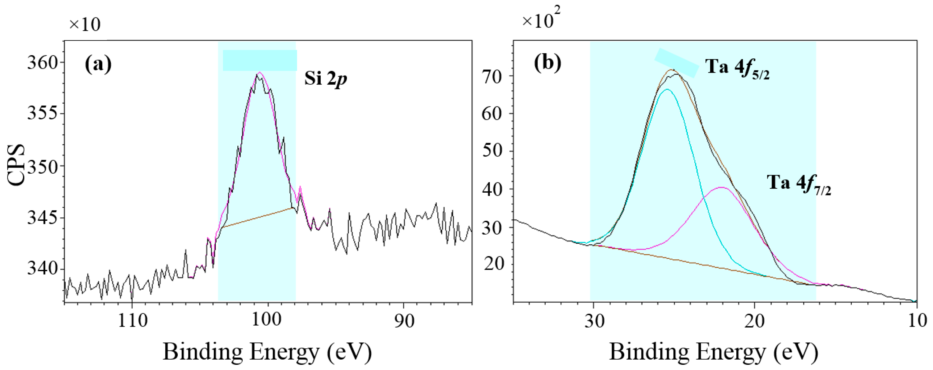
The high-resolution Si 2p and Ta 4f deconvoluted XPS peaks for the film deposited with 15% N2/(N2 + Ar) are presented in Figure 4a,b, respectively. As shown in Figure 4a, the Si 2p peak is at higher binding energy (Si–N, ~101 eV) compared to that of pure Si (Si 2p, ~99 eV). The latter peak shift is indicative of the transition to a Silicon-nitride chemical state. As far as the Ta 4f peak is concerned, the doublet shows the binding energy of Ta 4f7/2 to be around 23.5 eV and that of Ta 4f5/2 to be close to 25.5 eV. These binding energies correspond to a chemical state of Ta in Ta–N (4f7/2 = 23 eV and 4f5/2 = 25 eV) [24,25]. Thus, the XPS results confirm formation of nitrides for both Si and Ta. The Ta and N binding state in magnetron sputtered Ta-N films are discussed in detail in Ref. [21].
3.3. Microstructural Investigation
Three films were selected, namely with 7%, 13%, and 15% N2/(N2 + Ar), for HRTEM analysis to develop an understanding of the role of the N2 percentage in the gas mixture on the microstructure of the Ta–Si–N films.
3.3.1. Ta–Si–N film deposited with 7% N2
The inset in Figure 5 is a typical SAED pattern taken from the central section of the film. The three diffractions shown as (1), (2), and (3) with 2.33 Å, 1.80 Å, and 1.51 Å lattice spacing, respectively, correspond to (101), (102), and (110) diffractions of hex Ta2N. As shown in the SAED pattern, the diffraction rings are discontinuous indicative of texture in the film consistent with the XRD (Figure 1). Figure 5 is a cross-section HRTEM image from the film showing nanograins ~5–15 nm in size. The presence of amorphous boundaries around the grains was not innately clear, however, and most of the disordered regions (1–2 monolayers thick) were distinguishable via slight changes in compositional contrast as indicated in Figure 5.
3.3.2. Ta–Si–N film deposited with 13% N2
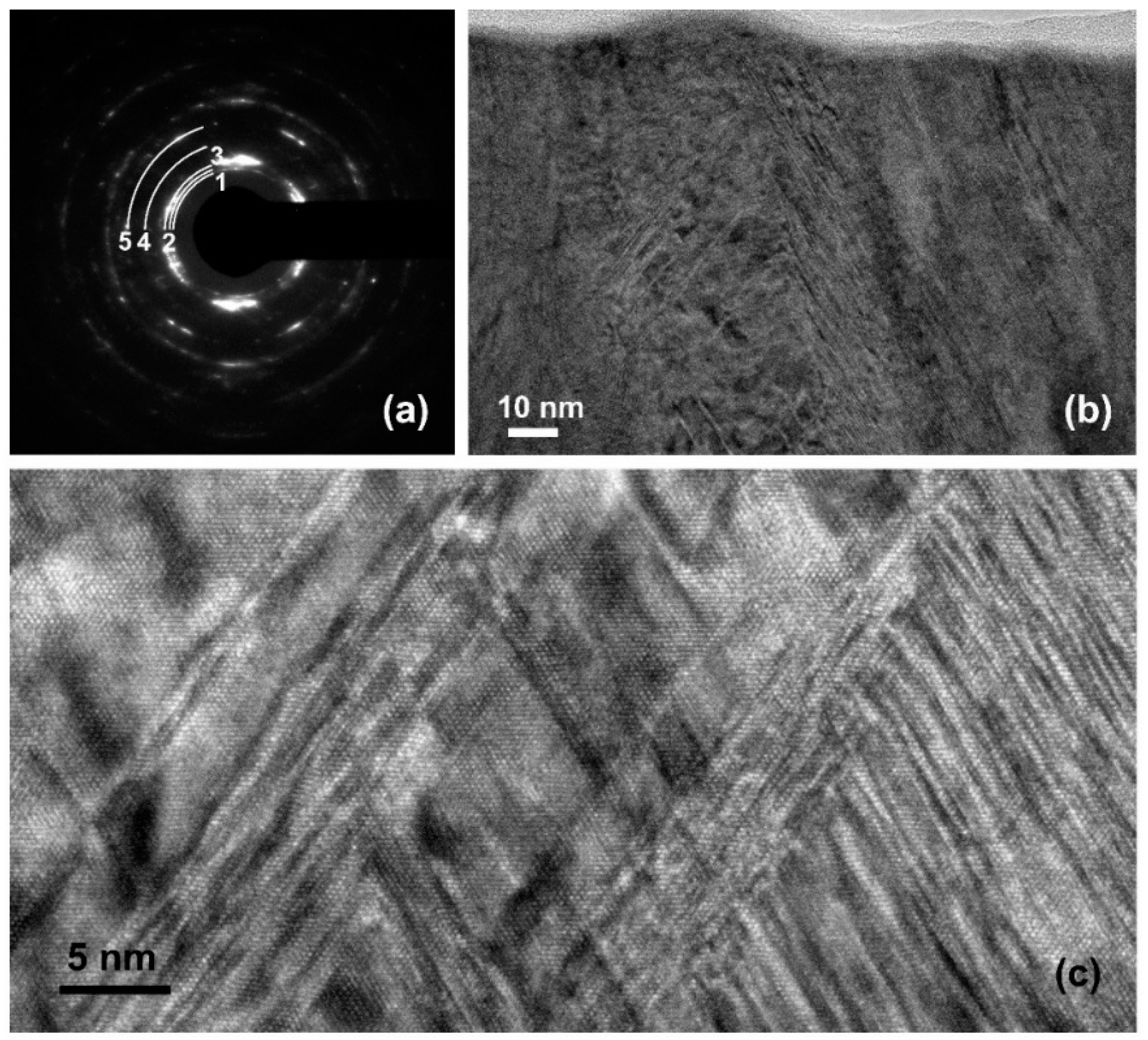
Figure 6a is a typical SAED pattern of the 13% N2 film. The five diffractions (1), (2), (3), (4), and (5) with lattice spacing 2.63 Å, 2.42 Å, 2.33 Å, 1.80 Å, and 1.51 Å, respectively correspond to (100), (002), (101), (102), and (110) diffractions of hex Ta2N. This is in good agreement with the XRD results for this film (Figure 1). However, the XRD did not show the (002) and (102) peaks of hex Ta2N. Also, the diffraction rings are discontinuous indicative of grain ordering in the columns in the in-plane direction in the film. A bright-field TEM micrograph of the bulk film structure is shown in Figure 6b. A sort of columnar morphology is evident in the film, with 20–30-nm-wide columns. Figure 6c shows a cross-section HRTEM micrograph within one of the columns. It is evident that the columns are composed of several nanocrystalline grains of different orientations. Closer observation shows that the columns are separated by an amorphous matrix of ~5–10 nm in width. As was seen in the AES results, this film had ~14%–15% Si, which has led to the possible formation of the disordered Si-N tissue phase between the columns. Similar observations of microstructural refinement caused by Si have been made in TiSiN [26] and Hf–Si–B [27] films.
3.3.3. Ta–Si–N film deposited with 15% N2
A typical SAED pattern of this film revealing several diffractions is shown in Figure 7a. The diffraction rings (1) and (3) with spacing of 2.65 Å and 2.29 Å, respectively, were identified as the (100) and (101) planes of hex Ta2N. The diffractions (2) between ring (1) an (3) have a lattice spacing of 2.5 Å and corresponds to (111) of fcc TaN. The diffraction spots (4) and (5) have a lattice spacing of 1.82 Å and 1.5 Å corresponding to the (102) and (110) diffraction of hex Ta2N, respectively. The (200) of fcc TaN and (002) hex Ta2N diffractions with lattice spacing 2.24 Å and 2.42 Å, respectively, could not be differentiated in the diffused arcs. This is in good agreement with the XRD results showing a broad transition peak, Figure 1, where only three peaks were well differentiated. Those were the (100) and (101) diffractions of hex Ta2N and the (111) diffraction of fcc TaN. Figure 7b is a bright-field TEM image of the bulk structure of the film clearly showing signs of a columnar morphology, columns being 20–30 nm wide. Figure 7c is a HRTEM images showing columns of two crystallographic orientations, possibly from two different phases (hex Ta2N and fcc TaN). These two phases are present in a characteristic microstructure composed of fine nanoneedles. The presence of amorphous boundaries in this film was not as clear as in the 13% N2 film. However, disordered tissue phase in this film can be differentiated via compositional contrast. The AES results depicted decrease in Si content to ~9% (from ~14% for 13% N2 film) for this film possibly due to formation of the additional N-rich TaN phase, which led to decrease in available N for Si to react and form a significant amount of the Si–N tissue phase.
3.4. Mechanical and Tribological Properties
Nanoindentation measurements were performed to investigate the effect of the N2 percentage in the gas mixture on the mechanical behavior of the Ta–Si–N films. The hardness response, effective modulus and level of residual stress of the films as a function of the N2 content are shown in Figure 8. The hardness was found to increase from ~30 to ~42 GPa as the N2 content increased from 7% to 15%. The same trend is observed for the effective modulus. The hardness increase can be attributed to several reasons. One of the possible reasons is the change in crystal structure from a textured hex Ta2N (for the 7% N2 film) to a more uniform hex Ta2N (for the 10% and 13% N2 films) structure. The 15% N2 film depicted the highest hardness of ~42 GPa. The hardness observed for this film is attributed to its dense nanocolumnar structure (~10–15 nm wide columns) composed of nanocrystalline needles with different crystallographic orientations within these columns, Figure 7c,d. This nanostructure is reported to result in hardness enhancement due to its resistance to dislocation motion because of the transition in crystallographic directions [28,29,30]. The hardness of the 13% N2 film was somewhat lower (~39 GPa) than that of the 15% N2 film. Although this film had hex Ta2N nanograins and a dense nanocolumnar structure, the nanograins were more of an equiaxed shape, Figure 6c, compared to the fine nanoneedle structure observed in the 15% N2 film. The nanoindentation of the film with 20% N2 was not carried out as the film surface was cracked possibly due to high residual stress (~5 GPa). The residual compressive stresses for the films increased from ~1 GPa to ~2 GPa as N2 increased from 7% to 15%. This increase could be due to incorporation of N atoms at interstitial sites at higher N2 content. The 20% N2 film exhibited a large residual stress (~5 GPa) and this was the reason it fractured during nanoindentation testing.
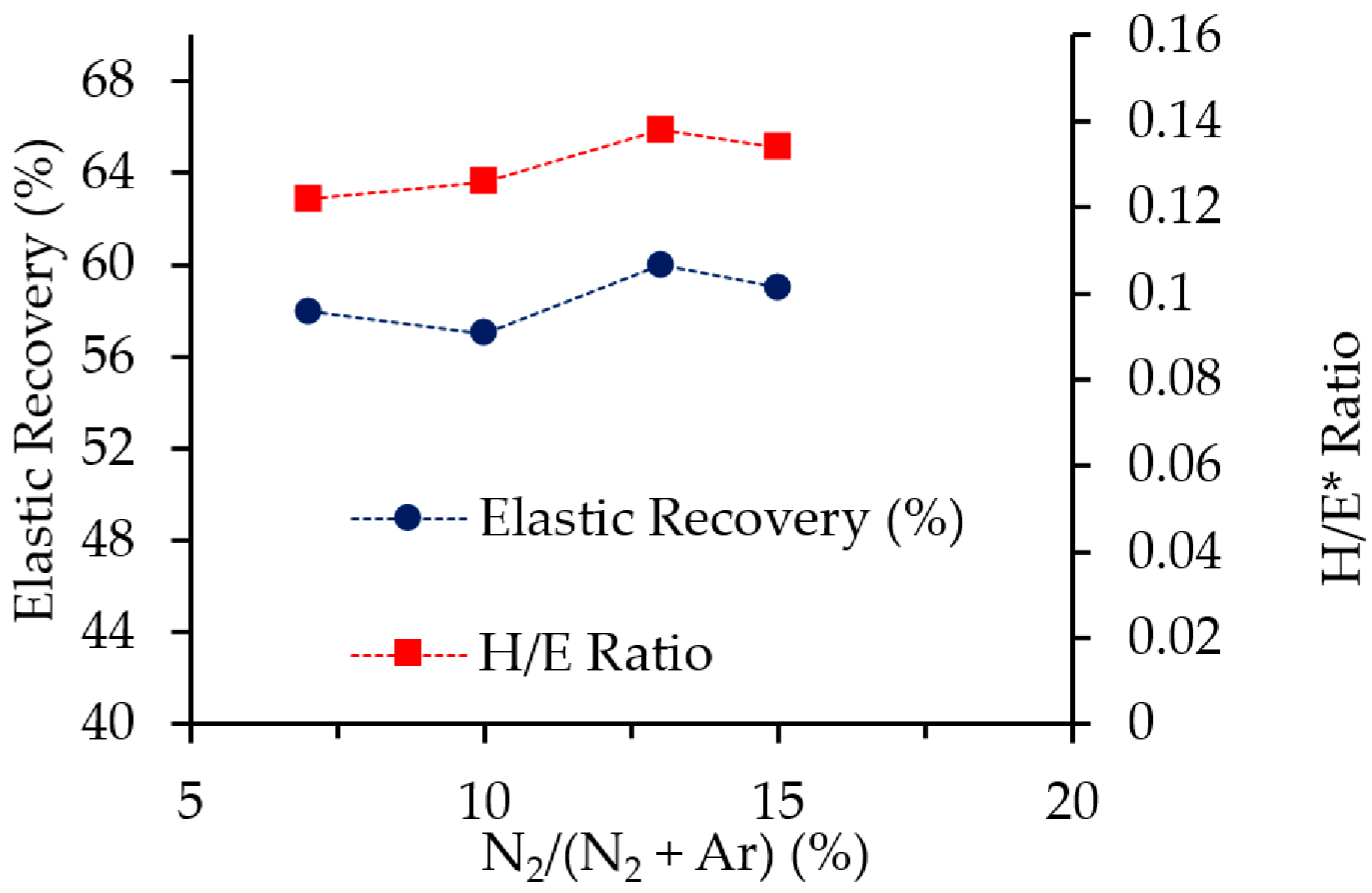
Figure 9 shows the H/E* ratio and elastic recovery We (%) of the films as a function of the N2 content. The H/E* ratio for all films is ≥0.11, reaching a maximum value of ~0.13 for the 13% N2 film, indicating development of high resistance to plastic deformation with increase in N2 content. Elastic recovery for all films is ~58% ± 2%. Elastic recovery of ~60% in hard films is expected to induce more resistance to cracking [28,31]. The results show that the films with N2 content ~10%–15% possessed a good combination of hardness (~40 ± 2 GPa) and residual stresses (~1.5 GPa). Especially, the 15% N2 film, in addition to highest hardness and low residual stress, exhibited high H/E* of ~0.13 and elastic recovery of ~60%.
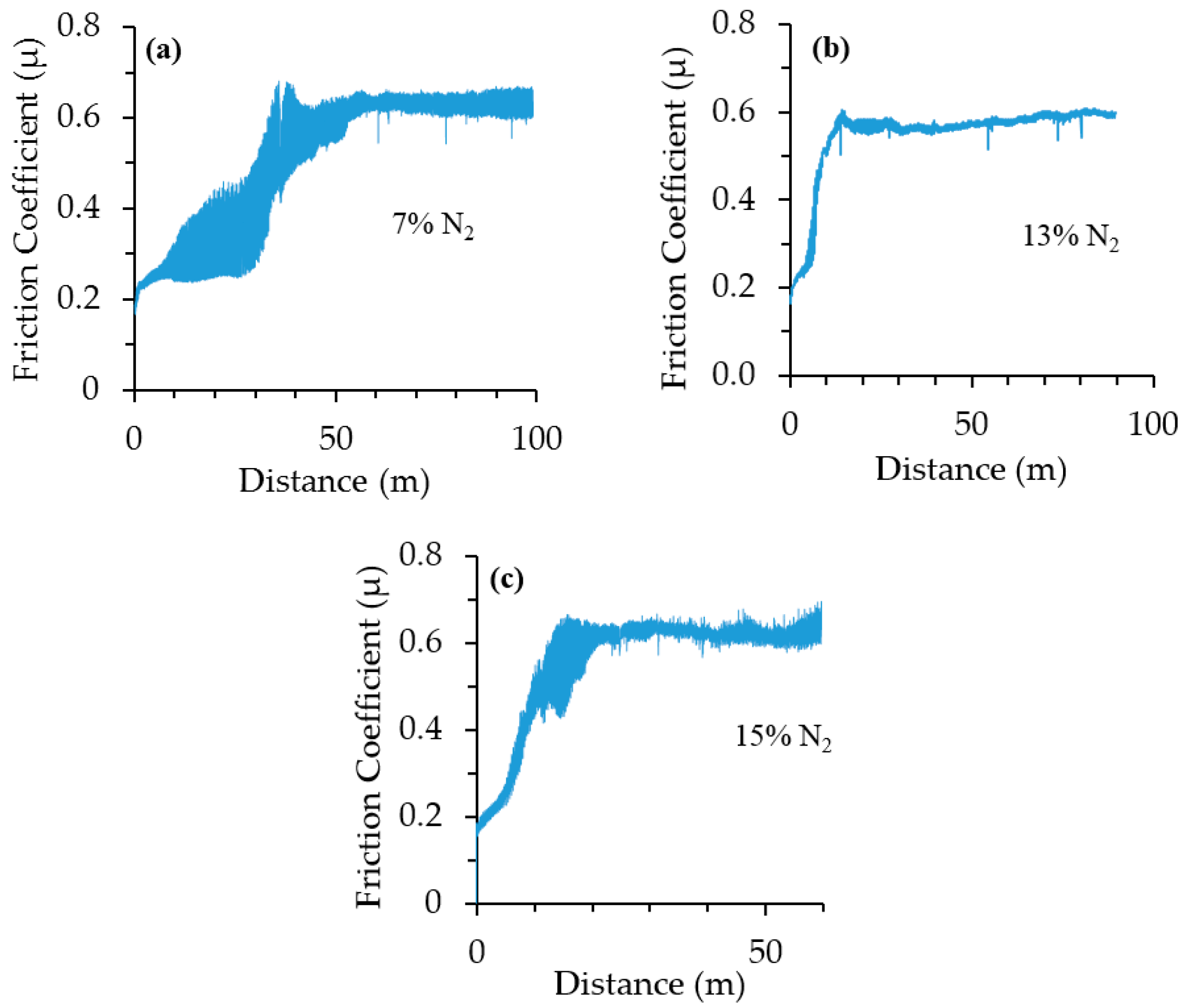
Pin on disc testing was performed on Ta–Si–N films deposited with 7%, 13%, and 15% N2 content. The friction coefficient was recorded continuously during wear testing and was ~0.6–0.7 for all films as shown in Figure 10a–c. Figure 11a–c shows the 2-dimensional wear track profile for these films. As seen, the wear track was much wider in the case of 7% and 13% N2 films (~100 μm) compared to the 15% N2 film (~40 μm). However, the depth of the wear track was lower for the 7% and 13% N2 films (~0.12–0.14 μm) compared to that of the 15% N2 film (~0.36 μm). The calculated wear rate for 7%, 13%, and 15% N2 films was 3.05 × 10⁻⁵, 7.09 × 10⁻⁶, and 1.28 × 10⁻⁵ mm3/N·m, respectively. The results show that the wear rate for the 13% film is almost an order of magnitude lower than the rest of the films. The lower wear rate of the 13% film can be attributed to its high hardness and uniform microstructure. This is also reflected in its smooth friction profile compared to the rest two films, Figure 10b. This film exhibited a microstructure composed of equiaxed hex Ta2N nanograins within a columnar structure separated by amorphous boundaries. On the other hand, the 7% film had lower hardness than the 13% film and textured structure, contributing to its higher wear rate. The 15% film, though had the highest hardness, the presence of the hard but brittle nanoneedles in its microstructure resulted in narrow by highly localized wear-induced cracking as is evident by its wear profile, Figure 11c.
3.5. Oxidation Resistance
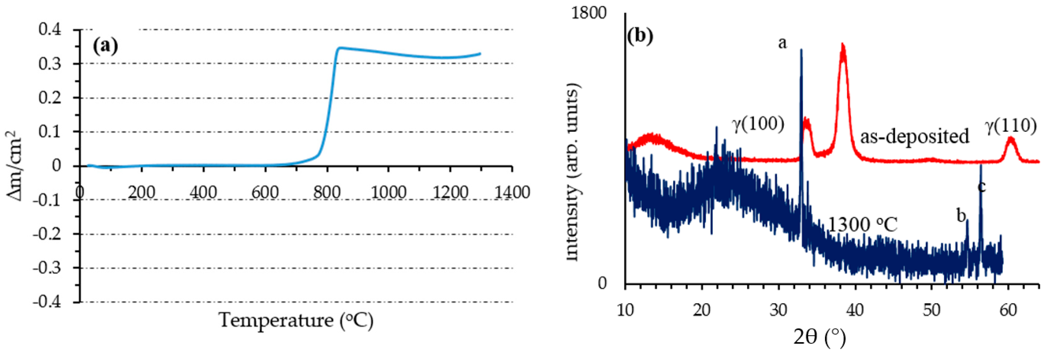
The 13% N2 film was selected to be tested for oxidation resistance. Thermogravimetric analysis was carried out to observe the oxidation behavior. The amount of weight change in the film was obtained as a function of increasing temperature in open air. Figure 12a presents the TGA response. The film was heated from room temperature to 1300 °C with a rate of 10 °C min−1 in flowing air. The TGA curve reveals no mass gain till ~780 °C and the beginning of mass increase after 780 °C which depicts the formation of Tantalum oxide. The mass gain continues up to 830 °C and then stabilizes up to 1300 °C the (maximum testing temperature). The saturation of the mass growth can be attributed to either formation of a stable surface protective oxide layer or to the oxidation of the entire bulk of the film. Figure 12b shows the XRD of the 13% N2 film before and after oxidation up to 1300 °C. XRD of the as-deposited film, which has been discussed earlier, revealed three diffraction peaks at 2θ angles of 33.7°, 38.5°, and 60.2°. These can be identified as the (100), (101), and (110) peaks of hex Ta2N (PDF#26-0985), respectively. The XRD of the film after annealing revealed three diffraction peaks at 2θ angles of 32.9°, 54.8°, and 56.1°. The first two peaks can be attributed to the (211), (400) diffractions of cubic Ta2O structure (PDF 18-1302), and the last peak can be attributed to the (132) diffraction of orthorhombic Ta2O5 structure (PDF 25-0922). It is evident from the comparison of the two scans that the entire film had been oxidized by testing up to 1300 °C.
It should be noted that the vast majority of the previous work on Ta–Si–N films has been concerned with amorphous and high Si content films [17,19,20,32,33]. These amorphous Ta–Si–N films can exhibit high temperature oxidation resistance but they are soft due to their amorhpous structure [28]. The present study focused on low Si content films resulting in nanocrystalline structures with high hardness (up to ~40 GPa) while maintaining high oxidation resistance up to 780 °C. Such a combination of properties makes the present films attractive candidates for protective coating applications ranging from gate electrodes and diffusion barriers in electronic devices to protective hard coating in glass molding dies.
4. Conclusions
The effect of the N2 content in the gas mixture on magnetron sputtered Ta–Si–N films was studied. It was found that the N2 content in the plasma greatly affects the structure, microstructure, and mechanical properties of the coatings.
Increasing the N2 content was found to cause a change in the film structure from textured hex Ta2N (7% N2) to uniform hex Ta2N (10% and 13% N2), a mixture of hex Ta2N and fcc TaN, to finally fcc TaN structure. Films with dense columnar morphology with and without the presence of amorphous boundaries were formed. Increasing the content of N2 from 7% to 10% and 13%, the texture greatly decreased and led to the formation of more uniform hex Ta2N phase, with columnar morphology composed of hex Ta2N nanograins separated by amorphous boundaries. Increasing the N2 content was found to increase the hardness of films deposited with 13% and 15% N2 exhibiting high hardness ~40 GPa. All films possessed a ratio of H/E* > 0.11 and an elastic recovery of ~60%. The film deposited with 13% N2 exhibited an excellent combination of high hardness (~39 GPa), high H/E* ratio (0.13), relatively low friction coefficient (~0.6), low wear rate (7.09 × 10⁻⁶ mm3/N·m), and was thermally stable up to 800 °C. Thus, this film has high potential for diverse industrial applications demanding high hardness along with high temperature oxidation resistance.
Author Contributions
A.Z. conducted the experiments, E.I.M. supervised the work, A.Z. and E.I.M. conducted the analysis and wrote the manuscript, and Y.S. and A.Z. conducted the TEM investigation; all authors reviewed and commented on the manuscript.
Funding
This research was supported in part by the U.S. National Science Foundation under Award No. NSF/CMMI DMREF-1335502.
Acknowledgments
The authors would like to thank Jiechao Jiang at the University of Texas at Arlington and researchers at IMDEA Madrid, Spain for their assistance with XPS and nanoindentations, respectively.
Conflicts of Interest
The authors declare no conflict of interest.
References
- Holleck, H.; Schier, V. Multilayer PVD coatings for wear protection. Surf. Coat. Technol. 1995, 76, 328–336. [Google Scholar] [CrossRef]
- Meletis, E.I. Wear-corrosion behavior of ion-plated thin films. J. Mater. Eng. 1989, 11, 159–167. [Google Scholar] [CrossRef]
- Cheng, Y.H.; Browne, T.; Heckerman, B.; Meletis, E.I. Mechanical and tribological properties of nanocomposite TiSiN coatings. Surf. Coat. Technol. 2010, 204, 2123–2129. [Google Scholar] [CrossRef]
- Nakao, S.; Numata, M.; Ohmi, T. Thin and low-resistivity tantalum nitride diffusion barrier and giant-grain copper interconnects for advanced ULSI metallization. J. Appl. Phys. 1999, 38, 2401–2405. [Google Scholar] [CrossRef]
- Leng, Y.X.; Sun, H.; Yang, P.; Chen, J.Y.; Wang, J.; Wan, G.J.; Huang, N.; Tian, X.B.; Wang, L.P.; Chu, P.K. Biomedical properties of tantalum nitride films synthesized by reactive magnetron sputtering. Thin Solid Films 2001, 398–399, 471–475. [Google Scholar] [CrossRef]
- Mori, H.; Imahori, J.; Oku, T.; Murakami, M. Diffusion barriers between Si and Cu. In Proceedings of the AIP Conference, Tokyo, Japan, 4–6 June 1997; Okabayashi, H., Shingubara, S., Ho, P.S., Eds.; AIP Publishing: Tokyo, Japan, 1998; Volume 418, p. 475. [Google Scholar] [CrossRef]
- Oya, G.I.; Onodera, Y. Phase transformations in nearly stoichiometric NbNx. J. Appl. Phys. 1976, 47, 2833–2840. [Google Scholar] [CrossRef]
- Massalski, T.B.; Okamoto, H.; Subramanian, P.R.; Kacprzak, L. Binary Alloy Phase Diagrams, 2nd ed.; ASM International: Materials Park, OH, USA, 1990; p. 2703. [Google Scholar]
- Bernoulli, D.; Müller, U.; Schwarzenberger, M.; Hauert, R.; Spolenak, R. Magnetron sputter deposited tantalum and tantalum nitride thin films: An analysis of phase, hardness and composition. Thin Solid Films 2013, 548, 157–161. [Google Scholar] [CrossRef]
- Nie, H.B.; Xu, S.Y.; You, L.P.; Yang, Z.; Wang, S.J.; Ong, C.K. Structural and electrical properties of tantalum nitride thin films fabricated by using reactive radio-frequency magnetron sputtering. Appl. Phys. A 2001, 73, 229–236. [Google Scholar] [CrossRef] [Green Version]
- Valleti, K.; Subrahmanyam, A.; Joshi, S.V.; Phani, A.R.; Passacantando, M.; Santucci, S. Studies on phase dependent mechanical properties of dc magnetron sputtered TaN thin films: Evaluation of super hardness in orthorhombic Ta4N phase. J. Phys. D Appl. Phys. 2008, 41, 045409. [Google Scholar] [CrossRef]
- Riekkinen, T.; Molarius, J.; Laurila, T.; Nurmela, A.; Suni, I.; Kivilahti, J.K. Reactive sputter deposition and properties of TaxN thin films. Microelectron. Eng. 2002, 64, 289–297. [Google Scholar] [CrossRef]
- Wittmer, M.; Melchior, H.J. Applications of TiN thin films in silicon device technology. Thin Solid Films 1982, 93, 397–405. [Google Scholar] [CrossRef]
- Münz, W.D. Titanium aluminum nitride films—A new alternative to TiN coatings. J. Vac. Sci. Technol. A 1986, 4, 2717–2725. [Google Scholar] [CrossRef]
- Choi, J.B.; Cho, K.; Lee, M.H.; Kim, K.H. Effects of Si content and free Si on oxidation behavior of Ti–Si–N coating layers. Thin Solid Films 2004, 447–448, 365–370. [Google Scholar] [CrossRef]
- Castaldi, L.; Kurapov, D.; Reiter, A.; Shklover, V.; Schwaller, P.; Patscheider, J. High temperature phase changes and oxidation behavior of Cr–Si–N coatings. Surf. Coat. Technol. 2007, 202, 781–785. [Google Scholar] [CrossRef]
- Chen, Y.I.; Lin, K.I.; Wang, H.H.; Cheng, Y.R. Characterization of Ta–Si–N coatings prepared using direct current magnetron co-sputtering. Appl. Surf. Sci. 2014, 305, 805–816. [Google Scholar] [CrossRef]
- Frety, N.; Bernard, F.; Nazon, J.; Sarradin, J.; Tedenac, J.C. Copper diffusion into silicon substrates through TaN and Ta/TaN multilayer barriers. J. Phase Equilib. 2006, 27, 590–597. [Google Scholar] [CrossRef]
- Zeman, H.; Musil, J.; Zeman, P. Physical and mechanical properties of sputtered Ta–Si–N films with a high (≥40 at %) content of Si. J. Vac. Sci. Technol. A 2004, 22, 646–649. [Google Scholar] [CrossRef]
- Nah, J.W.; Hwang, S.K.; Lee, C.M. Development of a complex heat resistant hard coating based on (Ta, Si)N by reactive sputtering. Mater. Chem. Phys. 2000, 62, 115–121. [Google Scholar] [CrossRef]
- Zaman, A.; Meletis, E.I. Microstructure and mechanical properties of TaN thin films prepared by reactive magnetron sputtering. Coatings 2017, 7, 209. [Google Scholar] [CrossRef]
- Adjaottor, A.A.; Ma, E.; Meletis, E.I. On the mechanism of intensified plasma-assisted processing. Surf. Coat. Technol. 1997, 89, 197–203. [Google Scholar] [CrossRef]
- Veprek, S.; Karvankova, P.; Veprek-Heijman, M.G.J. Possible role of oxygen impurities in degradation of nc-TiN/a-Si3N4 nanocomposites. J. Vac. Sci. Technol. B 2005, 23, L17–L21. [Google Scholar] [CrossRef]
- Chang, C.C.; Jeng, J.S.; Chen, J.S. Microstructural and electrical characteristics of reactively sputtered Ta–N thin films. Thin Solid Films 2002, 413, 46–51. [Google Scholar] [CrossRef]
- Arshi, N.; Lu, J.; Lee, C.G.; Koo, B.H.; Ahmed, F. Effects of nitrogen content on the phase and resistivity of TaN thin films deposited by electron beam evaporation. JOM 2014, 66, 1893–1899. [Google Scholar] [CrossRef]
- Cheng, Y.H.; Browne, T.; Heckerman, B.; Gannon, P.; Jiang, J.C.; Meletis, E.I.; Bowman, C.; Gorokhovsky, V. Influence of Si content on the structure and internal stress of nanocomposite TiSiN coatings deposited by large area filtered arc method. J. Phys. D Appl. Phys. 2009, 42, 125415. [Google Scholar] [CrossRef]
- Zhang, M.; Jiang, J.C.; Mareš, P.; Houška, J.; Vlček, J.; Meletis, E.I. Effect of the Si content on the microstructure of hard, multifunctional Hf–B–Si–C films prepared by pulsed magnetron sputtering. Appl. Surf. Sci. 2015, 357, 1343–1354. [Google Scholar] [CrossRef]
- Musil, J. Hard nanocomposite coatings: Thermal stability, oxidation resistance and toughness. Surf. Coat. Technol. 2012, 207, 50–65. [Google Scholar] [CrossRef]
- Lim, Y.L.; Chaudhri, M.M. The influence of grain size on the indentation hardness of high-purity copper and aluminium. Philosl. Mag. A 2002, 82, 2071–2080. [Google Scholar] [CrossRef]
- Zhang, M.; Jiang, J.; Houska, J.; Kohout, J.; Vlcek, J.; Meletis, E.I. A study of the microstructure evolution of hard Zr–B–C–N films by high-resolution transmission electron microscopy. Acta Mater. 2014, 77, 212–222. [Google Scholar] [CrossRef]
- Leyland, A.; Matthews, A. On the significance of the H/E ratio in wear control: A nanocomposite coating approach to optimised tribological behaviour. Wear 2000, 246, 1–11. [Google Scholar] [CrossRef]
- Zeman, P.; Musil, J.; Daniel, R. High-temperature oxidation resistance of Ta–Si–N films with a high Si content. Surf. Coat. Technol. 2006, 200, 4091–4096. [Google Scholar] [CrossRef]
- Chen, Y.-I.; Gao, Y.-X.; Chang, L.-C. Oxidation behavior of Ta–Si–N coatings. Surf. Coat. Technol. 2017, 332, 72–79. [Google Scholar] [CrossRef]
Figure 1.
Low-angle XRD of Ta–Si–N films deposited with varying the N2/(N2 + Ar) percentage.
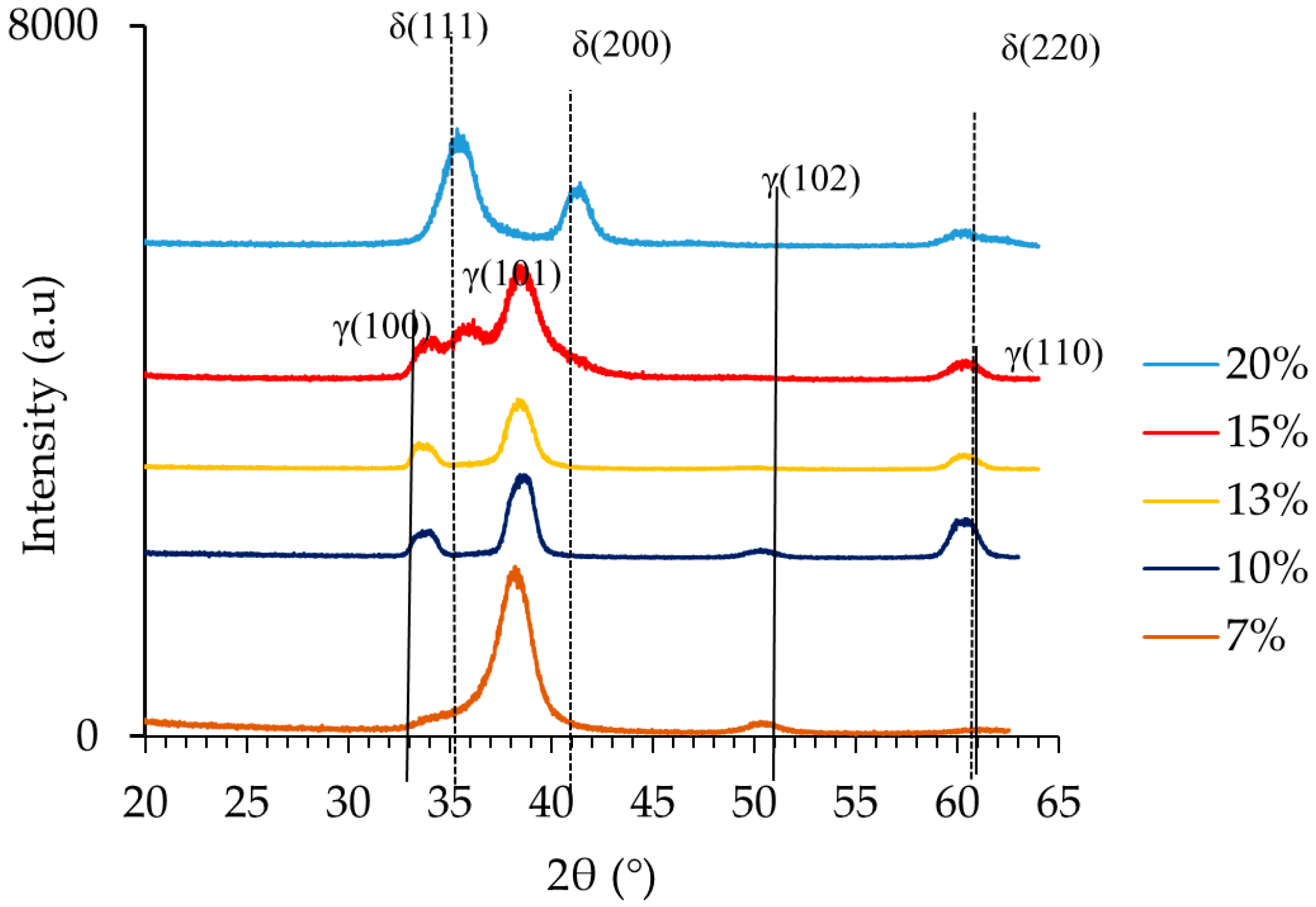
Figure 2.
Variation of the deposition rate of Ta–Si–N films as a function of the N2/(N2 + Ar) percentage.
Figure 2.
Variation of the deposition rate of Ta–Si–N films as a function of the N2/(N2 + Ar) percentage.
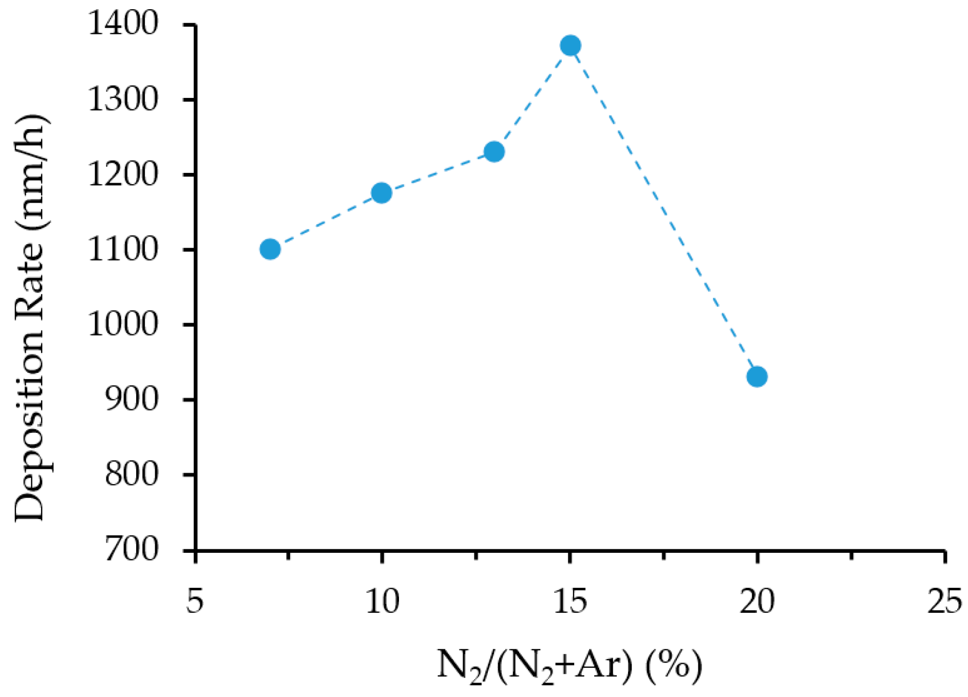
Figure 3.
Composition of the Ta–Si–N films as a function of the N2 percentage in the gas mixture.

Figure 4.
High-resolution deconvoluted spectra of (a) Si 2p and (b) Ta 4f core levels. (CPS: counts per second.).
Figure 4.
High-resolution deconvoluted spectra of (a) Si 2p and (b) Ta 4f core levels. (CPS: counts per second.).

Figure 5.
Cross-section high-resolution transmission electron microscopy (HRTEM) image of the 7% N2 film (inset is the selected-area electron diffraction (SAED) pattern).
Figure 5.
Cross-section high-resolution transmission electron microscopy (HRTEM) image of the 7% N2 film (inset is the selected-area electron diffraction (SAED) pattern).

Figure 6.
(a) SAED pattern, (b) Bright-field TEM micrograph of the structure and (c) cross-section HRTEM image of the 13% N2 film.
Figure 6.
(a) SAED pattern, (b) Bright-field TEM micrograph of the structure and (c) cross-section HRTEM image of the 13% N2 film.

Figure 7.
(a) SAED pattern, (b) Bright-field TEM image of the bulk film structure and (c) cross-section HRTEM image of the 15% N2 film.
Figure 7.
(a) SAED pattern, (b) Bright-field TEM image of the bulk film structure and (c) cross-section HRTEM image of the 15% N2 film.

Figure 8.
Variation in hardness, Young’s modulus and residual stress for the films deposited with N2 varying from 7% to 15%.
Figure 8.
Variation in hardness, Young’s modulus and residual stress for the films deposited with N2 varying from 7% to 15%.

Figure 9.
Variation in H/E* ratio and elastic recovery We (%) of the films as a function of N2 content.
Figure 9.
Variation in H/E* ratio and elastic recovery We (%) of the films as a function of N2 content.

Figure 10.
Coefficient of friction of Ta–Si–N films deposited with (a) 7%, (b) 13%, and (c) 15% N2.

Figure 11.
Wear track profile for films sputtered with (a) 7%, (b) 13%, and (c) 15% N2 content.

Figure 12.
(a) TGA response of Ta–Si–N film deposited with 13% N2 showing weight change per unit area (Δm/cm2) and (b) XRD of the 13% N2 film before and after oxidation.
Figure 12.
(a) TGA response of Ta–Si–N film deposited with 13% N2 showing weight change per unit area (Δm/cm2) and (b) XRD of the 13% N2 film before and after oxidation.

© 2019 by the authors. Licensee MDPI, Basel, Switzerland. This article is an open access article distributed under the terms and conditions of the Creative Commons Attribution (CC BY) license (http://creativecommons.org/licenses/by/4.0/).
Share and Cite
MDPI and ACS Style
Zaman, A.; Shen, Y.; Meletis, E.I. Microstructure and Mechanical Property Investigation of TaSiN Thin Films Deposited by Reactive Magnetron Sputtering. Coatings 2019, 9, 338. https://doi.org/10.3390/coatings9050338
AMA Style
Zaman A, Shen Y, Meletis EI. Microstructure and Mechanical Property Investigation of TaSiN Thin Films Deposited by Reactive Magnetron Sputtering. Coatings. 2019; 9(5):338. https://doi.org/10.3390/coatings9050338
Chicago/Turabian StyleZaman, Anna, Yi Shen, and Efstathios I. Meletis. 2019. "Microstructure and Mechanical Property Investigation of TaSiN Thin Films Deposited by Reactive Magnetron Sputtering" Coatings 9, no. 5: 338. https://doi.org/10.3390/coatings9050338
Note that from the first issue of 2016, this journal uses article numbers instead of page numbers. See further details here.