Article

Design and Prototyping Flow of Flexible and Efficient NISC-Based Architectures for MIMO Turbo Equalization and Demapping
 †

1
School of Engineering, Lebanese International University, Beirut 1105, Lebanon
2
Department of Electronics, UMR CNRS 6285 Lab-STICC, Telecom Bretagne, Brest 29238, France
3
Department of Physics and Electronics, Lebanese University, Hadath 1003, Lebanon
*
Author to whom correspondence should be addressed.
This paper is an extended version of our paper published in IEEE International Symposium on Rapid System Prototyping (RSP), 16–17 October 2014, as M. Rizk, A. Baghdadi, M. Jezequel, Y. Mohanna and Y. Atat. “Design and prototyping flow of NISC-based flexible MIMO turbo-equalizer”.
Electronics 2016, 5(3), 50; https://doi.org/10.3390/electronics5030050
Submission received: 31 March 2016 / Revised: 25 July 2016 / Accepted: 22 August 2016 / Published: 30 August 2016

Abstract

:
In the domain of digital wireless communication, flexible design implementations are increasingly explored for different applications in order to cope with diverse system configurations imposed by the emerging wireless communication standards. In fact, shrinking the design time to meet market pressure, on the one hand, and adding the emerging flexibility requirement and, hence, increasing system complexity, on the other hand, require a productive design approach that also ensures final design quality. The no instruction set computer (NISC) approach fulfills these design requirements by eliminating the instruction set overhead. The approach offers static scheduling of the datapath, automated register transfer language (RTL)synthesis and allows the designer to have direct control of hardware resources. This paper presents a complete NISC-based design and prototype flow, from architecture specification till FPGA implementation. The proposed design and prototype flow is illustrated through two case studies of flexible implementations, which are dedicated to low-complexity MIMO turbo-equalizer and a universal turbo-demapper. Moreover, the flexibility of the proposed prototypes allows supporting all communication modes defined in the emerging wireless communication standards, such LTE, LTE-Advanced, WiMAX, WiFi and DVB-RCS. For each prototype, its functionality is evaluated, and the resultant performance is verified for all system configurations.

1. Introduction

To follow the evolution in wireless communication applications, the rapid design and implementation of embedded systems are vital factors. Reducing the development cycle of hardware designs is greatly demanded in order to meet market pressure. The realization of the hardware prototypes is required to be within a short time to carry out on-chip system validation and to evaluate exactly the performance under various usage scenarios. On the other hand, the utility of application-specific processors is of an increasing extent, since they provide a good solution in designing efficient hardware architectures that can satisfy the tight constraints on the implementation area and power consumption and nowadays fulfill the requirements in terms of high throughput and low error-rate performance. These facts motivate exploiting design and prototype flows that are capable of providing high design quality, as well as increased design productivity. In addition, wireless digital communication standards are developing continuously. Consequently, the applications are becoming increasingly complex and diverse. Wireless digital communication standards, such as DVB-RCS [1] for digital video broadcasting, 802.11 (WiFi) [2] and 802.16 (WiMAX) [3] for wireless local and wide area networks and LTE and LTE-Advanced [4] for mobile phones, support a variety of system configurations related to channel codding type, modulation type, mapping styles and antenna dimensions for multiple-input multiple-output (MIMO) transmission techniques. In order to cope with the various configurations, flexible architecture designs comprise a key trend in implementing different components of the transmission scheme. This work concerns the design and the implementation of flexible and high performance application-specific processors dedicated to the equalizer and the demapper modules of the turbo-receiver. In contrast to a non-iterative receiver, an iterative receiver is characterized by the existence, in addition to forward paths, of feedback paths through which constituent units can send the information to previous units iteratively. On every new iteration, each block generates soft information depending on channel information and on received a priori soft information generated by other blocks in the previous iteration.
The concept of turbo equalization allows improving communication system performance by iteratively exchanging information between the soft-input soft-output (SISO) equalizer and the SISO channel decoder. It was initially introduced in [5] to alleviate the destructive effects of inter-symbol interference (ISI) for wireless digital transmission, which is protected by convolution codes. In modern communication systems, the use of MIMO raises co-antenna interference at the receiver side. Nowadays, to combat against ISI, orthogonal frequency-division multiplexing (OFDM) is mainly utilized. In a MIMO-OFDM system, where a receiver should address the effects of co-antenna interference, in addition to ISI, the concept of turbo equalization can be used to mitigate iteratively the co-antenna interference. Among different equalization methods, MIMO minimum mean-squared error (MMSE) is a prominent low-complexity suboptimal algorithm [6,7]. Using the MMSE algorithm in an iterative scheme compensates sub-optimality and leads to an error-rate performance near enough to the performance achieved when the optimal high-complexity maximum-likelihood (ML) algorithm is used [8,9].
Iterative demapping was proposed firstly in [10] based on bit interleaved coded modulation (BICM) with additional soft feedback from the SISO convolutional decoder to the constellation demapper. For a system with convolutional code, BICM and 8-PSK modulation, 1 dB and 1.5 dB gains for BER performance were reported for Rayleigh flat fading channels and channels with AWGN, respectively. In [11], the use of iterative demapping shows performance improvement of 1.2 dB at BER of 10 6 for the QAM BICM scheme with the ow-density parity-check (LDPC) channel decoder over a flat fading Rayleigh channel with 15% of erasures. The symbol-by-symbol maximum a posteriori (MAP) algorithm is the optimal algorithm for obtaining the outputs of the demapper. The MAP algorithm is likely to be considered of high complexity for hardware implementation in a real system basically because of the numerical representation of probabilities, non-linear functions and because of mixed multiplications and the additions of these values [12]. Implementing the MAP algorithm in its logarithmic domain instead of the probabilistic form reduces the computational complexity. The Max-Log-MAP demapping algorithm is a suboptimal direct transformation of the MAP algorithm into the logarithmic domain; hence, the values and operations are easier to handle. Figure 1 presents the MIMO-OFDM receiver block diagram, which uses MMSE turbo-equalization and turbo-demapping.
In previous work, presented in [13,14], flexible application-specific processors dedicated for turbo-equalization and turbo-demapping have been proposed. The first task in realizing a flexible multi-standard hardware component is to define the flexibility parameters. The equalizer module is based on the MMSE algorithm, and it is affected by flexibility parameters, which are extracted from the following requirements:
  • The ability to support various MIMO schemes reaching to a 4 × 4 antenna dimension
  • The capability of using efficiently the implemented hardware resources for different time diversity channel types (block fading, quasi-static and fast fading)
  • The possibility to execute in both iterative and no-iterative modes
Regarding turbo-demapping, the demapper implements the Max-Log-MAP algorithm. It embraces all flexibility requirements for recent wireless digital communication standards. It can execute in iterative and non-iterative processing schemes and support different mapping styles, modulation types and signal space diversity (SSD) with rotated constellation. Such wide flexibility becomes crucial in the current trend toward the convergence of wireless communication services [15] and the requirement of multi-standard terminals. In addition, the demonstration of the ability of designing highly flexible, yet efficient, hardware architectures can prompt the proposition of new processing schemes and parameters that better meet the environment conditions and applications. Such novel schemes, associated with efficient flexible implementations, can then constitute potential candidates for adoption in next generation communication systems.
In addition to the requirements of efficiency and productivity, the emergent flexibility requirement sets up a new design metric. The application-specific instruction set processor (ASIP) concept offers a trade-off in terms of the efficiency of the application-specific integrated circuit (ASIC) and the flexibility of the general purpose (GP) processor by customizing the datapath structure and functionality by using a custom instruction set. In cases where the tailored hardware is dedicated for a particular fixed application, the process of instructions’ specification and describing forms an overhead. Instead of dynamic scheduling, no instruction set computer (NISC) concept adopts static scheduling of operations to simplify the ASIP approach. Figure 2 shows the transition from the ASIP design approach to the NISC design approach.
By eliminating the task of finding and designing a custom instruction set, the design productivity is increased. Furthermore, the design quality is better achieved by shrinking the design complexity to match the exact requirements of the desired application. The typical controller functionalities, such as instruction decoding, dependency analysis and instruction scheduling, are carried out by the compiler in NISC. The compiler is responsible for scheduling operations and decoding them into control words (CWs), where each represents the group of control signals that must be loaded to the datapath components in every clock cycle. At run time, the CWs that are stored in the control memory are loaded by means of a simple controller, which applies the control signals to their corresponding components in the datapath. Moreover, an NISC-based architecture may be reused for different applications or various system configurations of the same application. Flexibility is attained by re-exploiting the hardware architecture design without any modifications on the structures of the datapath or controller. Different groups of control words are only re-generated statically and re-loaded to the control memory of the design.
In this paper, we aim to present in detail the entire design and prototype flow, starting from architecture specification till FPGA implementation, in addition to hardware validation and performance evaluation. The rest of this paper is organized as follows. The following section illustrates the proposed NISC architectures. The adopted prototyping flow is presented in details in Section 3. Section 4 presents the on-chip validation and summarizes the obtained results. Finally, Section 5 concludes the paper.

2. Designed NISC-Based Architectures

2.1. Equalizer Architecture

The designed NISC-based architecture, which is dedicated to MMSE equalization, is basically made of a control unit and the equalizer module called EquaNISC, which is the main core of the design. To meet with the demanded requirements of flexibility, the hardware resources are instantiated carefully and shared among different computations. Adequate hardware operators are implemented to perform all required computations taking into account the requirements of flexibility, efficiency and performance. Fixed-point arithmetic is adopted rather than floating-point arithmetic in order to reduce the implementation costs, while ensuring sufficient accuracy and negligible performance loss. Floating-point arithmetic is generally used to conduct performance evaluation studies of algorithms. This is typically limited to theoretical performance evaluation in terms of communication quality and error rates. For a practical implementation perspective, using fixed-point arithmetic instead of floating-point reduces significantly the implementation costs in terms of area occupation and energy consumption. In fixed-point architectures, the memory and bus widths are smaller, leading to a definitively lower cost and power consumption. Moreover, floating-point operators are more complex, having to deal with the exponent and the mantissa, and hence, their area and latency are greater than those of fixed-point operators [16]. All operands that are involved in MMSE computational operations are quantized in the 16-bit two’s complement representation according to carefully-determined precisions [17]. Temporal parallelism using a pipeline is applied to improve the performance and to increase the throughput. The designed architecture is shown in Figure 3, which presents the constituent units, as well as the input/output interface. The equalizer architecture receives input data from the soft mapper, the look-up table 1 x LUT and channel and control memories, which are called ChMem and CMem, respectively. ChMem stores the constant data of the channel, and CMem stores the control words generated statically by the NISC compiler. The 1 x LUT is used to replace the inversion operations, which are computationally demanding, in order to avoid undergoing expensive computations. The LUT uses memory instead of large numbers of computational elements. It includes all 16-bit inverse values, which are possibly used in the inversion process. These values are pre-computed and stored such that the value x intended to be inverted is used directly as the LUT index (address) to retrieve the inverse value 1 x . When using LUT, both resource utilization and propagation delay are reduced at the cost of accuracy. A detailed analysis and long numerical simulations have been conducted for different configurations to find the required data width and accurate precisions for the fixed-point representation of the involved values. Moreover, the size of the LUT adds additional overhead. However, the required memory space in this application is reasonable since the LUT depth is limited to 2 16 . To reduce the size of the LUT, the segmentation approach may be used by storing one inverse value, the median of the group, in the LUT to represent the results of 1 x for a group of consecutive values of x [18]. Other memory size reduction technique are achieved by storing only positive values in the LUT. In this case, the LUT depth is reduced from 2 m to 2 m 2 , where m is the number of bits representing the positive number.

2.1.1. Control Unit

The control unit has a simple architecture. Its main functionality is to load at run-time the proper control words stored in Cmem to the different components of the EquaNISC module. Moreover, the control unit manages the sequential activity of the design. It specifies the iteration number, as well as the order of symbols in the equalization process. Furthermore, the control unit produces notification signals about the equalizer activity, such as the readiness of output data at the end of the frame. Such signals are used to synchronize the equalizer model with input/output memory blocks and other components in the receiver scheme.

2.1.2. EquaNISC Module

EquaNISC is the principal module of the proposed architecture dedicated for MIMO MMSE linear turbo equalization. It is hierarchically composed of three units:
  • Storage unit (SU)
  • Multiplexing unit (MU)
  • Computational unit (CU)

Storage unit (SU):

SU is responsible for saving data loaded from memory blocks and the results of intermediate computations. It is composed of three groups (H, V and G) of 16-bit registers that each can store one 4 × 4 complex matrix. Inside the groups, registers are classified into couples such that each is proposed to store the real part and the imaginary part of a complex number. In addition to the register groups, four registers are instantiated to store the variance values.

Multiplexing unit (MU):

MU is responsible for arranging the data transfer in the EquaNISC module between internal units (storage unit and computational unit). Furthermore, it manages the flow of input/output data and reformulates it in order to match the desired quantization. It is composed of multiplexers that construct a connecting chain between different components of the architecture. For each multiple-input component, a multiplexer is allocated to manage its input data flow coming from different sources.

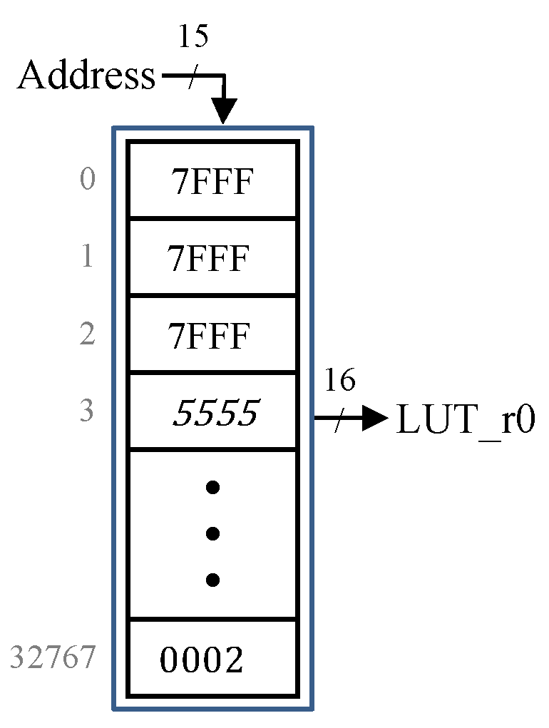
Computational unit (CU):

The CU contains all hardware resources that perform all required computation operations in the MMSE equalization algorithm. It spreads over six pipeline stages and includes all hardware operators, which are utilized in the execution of the required algorithmic computations. It incorporates carefully-designed modules, which are capable of using the allocated resources efficiently for different system configurations. For the additional details about the structures of each unit, the reader can refer to [13].

2.2. Demapper Architecture

The designed NISC-based architecture dedicated to the universal demapper, as any NISC-based architecture, is basically composed of the module, which performs the main functionality, which is referred to as DemaNISC, and a simple control unit. Figure 4 shows the hierarchical structure of the proposed architecture and its connections with input and output blocks. The inputs to the demapper architecture are the log-likelihood ratios (LLRs)from the decoder, variance σ 2 , control words, constellation information, received symbols, fading factors and the inverse values 1 2 x . Figure 4 shows several memory blocks. AprMem stores the a priori information (LLRs), which is provided by the channel decoder through the feedback path. The control words (CWs) generated by the NISC tool set compiler are saved in the CMem memory block. Constellation information is arranged in the Constellation LUT. YMem and ρMem include, respectively, the received symbols and fading factors collected from the channel or delivered by the equalizer module in case turbo equalization is adopted. The look-up table 1 2 x LUT contains the pre-computed inverse values required in inversion operations.

2.2.1. Control Unit

The control unit is mainly responsible for loading CWs, which are stored in the control memory CMem into the components of the DemaNISC module. In fact, it shares a similar architecture to the control unit used in the equalizer described in the previous chapter. To accomplish this functionality, the unit handles the address of CMem memory and constructs links to distribute the control-signal bits of CWs to appropriate components. In addition, the control unit manages the input data flow from YMem, ρMem and Constellation LUT. These basic tasks reveal the simple hardware structure required to implement the control unit.

2.2.2. DemaNisc Module

The DemaNisc module is considered the main core of the architecture design tailored to implement the Max-Log-MAP demapping algorithm. From a hierarchical scope, it can be viewed as a concatenation of five units:
  • Euclidean distance unit (EDU)
  • A priori LLR summation unit (ASU)
  • Inter-subtraction unit (ISU)
  • Minimum finders unit (MFU)
  • Output unit (OU)

Euclidean distance unit (EDU):

This unit incorporates all hardware resources that are involved in computing the Euclidean distance. It is provided by the in-phase (I) and the quadrature (Q) components of the received symbols y I and y Q , constellation symbols x I and x Q and fading factors ρ I and ρ Q , in addition to the noise variance σ 2 . At each computation, the Euclidean distance unit can deliver one two-dimensional distance or two one-dimensional distances.

A priori LLRs summation unit (ASU):

The hardware resources located in ASU generate the a priori LLRs summation of input LLRs, which are required in the case of turbo demodulation. The LLR values stored in AprMem memory and the vector v representing the binary mapping μ of symbols from the Constellation LUT are the inputs to this unit.

Inter-subtraction unit (ISU):

The a priori LLRs summation values generated by ASU are delivered to ISU, which subtracts them in parallel from the value of two-dimensional Euclidean distance calculated by EDU. To perform this functionality, ISU includes a subtractor set, which is made of eight real subtractors and sufficient registers to store the output results.

Minimum finders unit (MFU):

Minimum finders are established to compute the minimum functions required in the Max-Log-MAP algorithm. This unit integrates eight minimum finder blocks, the architecture of which is presented in Figure 5. Each block is concerned with finding the minimums associated with a bit location v i along all constellation symbols. For the additional details about the structures of each unit, the reader can refer to [14].

Output unit (OU):

The output unit is responsible for delivering the final LLR values corresponding to each bit. The inputs of this unit are the minimum values available in the registers of the minimum finders unit. Once the minimums of all constellation points are determined, this unit produces the difference between minimum pairs, which correspond to each bit location. The resultant differences are then stored in output registers.

3. Typical NISC Design Methodology

The NISC design approach offers an open source tool set [19] that can be used either as a free C-to-RTL(i.e., C to Verilog) synthesis tool or as a tool to design embedded custom processors. To design a custom processor dedicated to a specific application, the designer should specify first a datapath and a C code, which describes the target application. The formal ADL of the tool set, which is called generic netlist representation (GNR), captures the structural details of the datapath [20,21]. GNR describes the datapath as a netlist of components and assigns different attributes to each component. The component type can be a basic RTL component or a module, which is a hierarchical component composed of components described by another GNR module with their connections. The datapath of a NISC architecture can have several instances of each component type. A component instance should have a unique name and a type name that refers to a component description in the library. The datapath description also includes netlist connections.
The NISC compiler is then provided by the high-level description of the application and the GNR description of the datapath. The compiler maps the C code directly on the devised datapath and generates a finite state machine (FSM), which specifies the behavior of the datapath in each clock cycle. Then, the compiler runs netlist-constrained resource scheduling and binding techniques and later uses the FSM to generate the stream of control signals.
Corresponding to each control signal of each component in the datapath, a field is added to the control words. The NISC compiler produces “0”, “1” or “don’t care” values for the bits of the control words. A “don’t care” value (denoted by “X”) indicates that the corresponding unit is inactive at a given cycle, and its control signal can be assigned to “0” or “1” without affecting execution behavior. The structural information of the datapath is also processed (validated and completed) and then translated automatically by the tool set RTL generator into a synthesizable RTL design described in hardware description language (HDL)that is used later for simulation and synthesis.
After simulation, synthesis and placement and routing (PAR), the accurate timing, power and area information can be extracted and used for further datapath and/or application refinement. The NISC tool set generic design flow is shown in Figure 6. The flow enables the designer to iteratively refine and improve the results. The designer can initially start with a certain description of the application and use a specific datapath in order to execute the application and generate initial results. Later, the designer can modify iteratively the chosen application and/or the datapath and then utilize the NISC tool set to generate new results. In each iteration, the designer can concentrate separately on one quality metric, such as implementation area, clock frequency, parallelism, power consumption, etc. Finally, the designer can choose from multiple studies the design that best fits with his or her desired requirements.

4. Adopted Design Flow

To implement the NISC-based architectures dedicated for MMSE equalization and Max-log-MAP demapping, we used the NISC approach related design flow and tools. In this context, the typical direct compilation of C codes describing the functionality using the NISC tool set gives inefficient hardware results. In order to achieve high performance and efficient resource utilization, the direct control of hardware resources is devised using pre-bound functions, which are C-like functions mapped by the compiler to specific hardware resources [22]. For a specific module, a pre-bound function is defined by declaring the proper control values and the utilized input/output ports. Moreover, the scheduling information, such as the dependency, the execution stages and the timing, are specified. The PreboundCGenerator in the NISC tool set is later used in order to generate C definitions of pre-bound functions. These definitions are listed in the C application prior to the compilation on the given datapath. Figure 7 shows an overall presentation of the prototyping flow adopted in this work. The flow is divided into two levels: the NISC abstraction level and the FPGA implementation level.

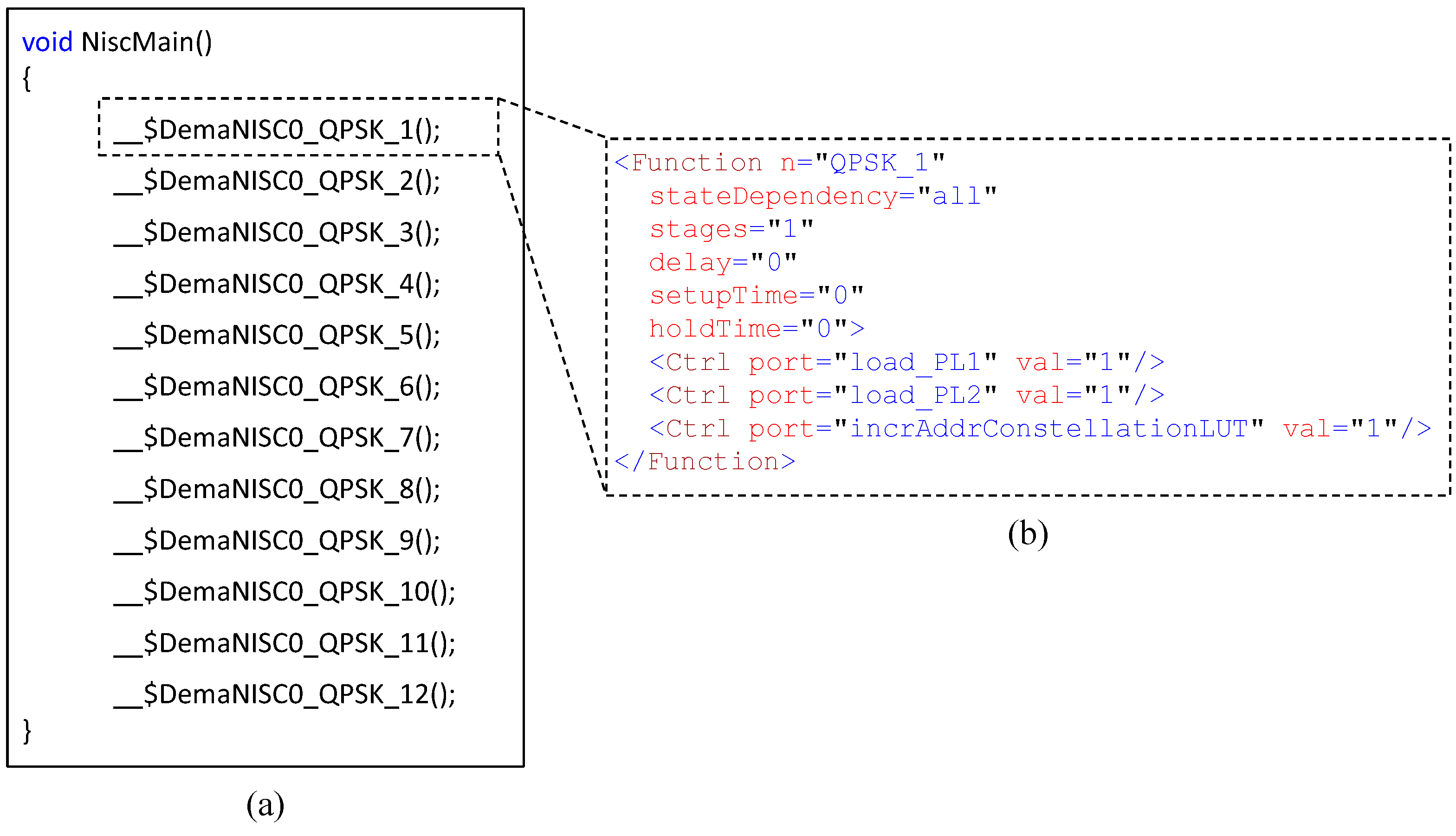
4.1. NISC Abstraction Level

The first step towards design development is to describe the datapath of the proposed architecture. The datapath is captured in (GNR). Using HDL description (i.e., Verilog), all basic components, such as multiplexers, adders, subtractors, multipliers, registers and converters, are first defined. In GNR, basic components are simply described by indicating their types, ports, parameters and aspects. Hierarchical modules (such as computational unit, multiplexing unit, storage unit and the EquaNisc module in the equalizer architecture; and Euclidean distance unit, the a priori LLR summation unit, inter-subtraction unit, minimum finders unit, output unit and the DemaNISC module in the demapper architecture) are built in GNR. A hierarchical module can be composed of basic component(s) and/or module(s) of lower hierarchical level. Figure 8 presents the GNR description of a minimum finder block used in minimum finders unit (MFU) of the DemaNISC module (Figure 5a). The figure illustrates the construction of the “MinFinder” module from basic blocks, such as multiplexers, subtractor, registers and logic gates, in addition to its internal netlist. The module has seven ports and is parametrized by three parameters (BIT_WIDTH, Mid_WIDTH and Initial), which are used as internal specifications and are defined by higher hierarchical level components. In each architecture, all required components and modules are allocated, and their attributes and interconnections are assigned. The automatic completion of the GNR description is exploited to reduce the datapath modeling. In addition, syntax checking and rule validation, which are provided by the tool set, are used to quickly detect and fix connection errors.
The following step after datapath description is to declare pre-bound functions defining the functionality of the EquaNISC/DemaNISC module. All control values that should be applied to control ports of hardware resources in a definite clock cycle are enumerated in a specific pre-bound function. All independent operations are merged into single pre-bound function in order to maximize the exploitation of hardware resources and to decrease the execution time. Figure 9 shows a pre-bound function sample, which merges several operations (four data transfers (move), one data loading from ChMem and setting a new address) into one pre-bound function “PreBoundSample”. As shown in the figure, in addition to scheduling information, all required control values of all incorporated resources and ports are specified explicitly. When all pre-bound functions are described, the PreboundCGenerator tool is utilized to process the structural description of all pre-bound functions and to generate their corresponding C definitions. A C code application is easily developed by listing the sequence of C definitions related to all pre-bound functions involved in MMSE equalization/Max-Log-MAP demapping. Figure 10a presents the list of C definitions that are related to pre-bound functions defining the functionality of the DemaNISC module. Figure 10b shows the GNR description of the pre-bound function “QPSK1”, which declares the control values that should be applied at the first step of demapping for the QPSK modulation scheme. The C application is verified by checking the code syntax and the availability of used C definitions of pre-bound functions. The last step in NISC abstraction level is to compile the datapath and the C code application. The tool set compiler is used to generate the control words, which are arranged automatically in the output memory file. The RTL generator in the tool set produces the HDL code, which describes the whole design architecture benefiting from the compiler information and the datapath structure.

4.2. FPGA Implementation Level
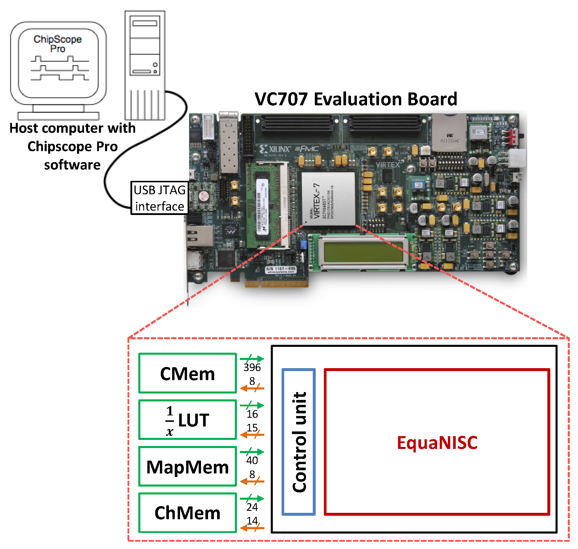
At the FPGA implementation level, Xilinx ISE tool suite is used to implement the designed architectures. For each architecture design, the HDL generated by NISC tool set describing the EquaNISC/DemaNISC module is imported into a new Xilinx ISE project. Furthermore, the simple architecture of the control unit, which is required to load the control words from control memory to the functional module, is provided in HDL. The Xilinx project is assumed to integrate the functional module (EquaNisc/DemaNISC), the control unit and the input memory blocks. The only missing elements, at this level, are the synthesizable memories. IP synchronous block memories of suitable parameters (type, depth, width) are generated by means of the Xilinx Core Generator. Block memories are chosen to be utilized in this prototype not to impose additional logic utilization rather than that occupied by the actual architecture in the final synthesis. Block memories are implemented in dedicated blocks in the FPGA. Adequate interface modules are constructed in order to realize the connection between memories and the architecture modules. The used memories are initialized by memory-content files. A fixed-point software reference model is used to generate automatically the contents of input memory blocks. Concerning control memory (CMem), the CWs generated by the compiler are utilized. The NISC tool set imposes a basic NISC architecture with supplementary hardware resources, such as the interrupt unit, data memory and combinational logic devices. Thus, the generated control words include extra control bits. In addition to control words related to the desired functions, the NISC compiler would generate control words that are responsible for the startup addressing, jump and call/return operations of C functions. These control words and the extra control signals do not impact the desired functional operation and form an additional overhead in terms of memory size. In our work, neither the added control words nor the control signals of the additional resources are taken into account. Only the sequence of control signals, which are related to the real functionality of the architecture, are extracted from the generated memory file and imported to control memory CMem.
With this complete model, sufficient simulations are conducted in order to confirm the proper functionality of the architecture for various system configurations. The simulations are performed to cover separate case studies with multitude characteristics concerning antenna dimensions, channel fading types, modulation schemes and mapping styles. Running simulations enables detecting the state of all internal signals and inspecting the flow of input and output data at each time slot. Figure 11 presents the simulation window of the equalizer architecture using Xilinx ISE. The simulation window shows the output signals of the equalizer architecture for 2 × 2 block fading mode. For this mode, the estimates relative to two successive symbol vectors ( x ˙ and x ¨ ) are generated concurrently. The figure shows the real and imaginary parts of the estimate symbols x 0 ˙ ˜ , x 1 ˙ ˜ , x 0 ¨ ˜ and x 1 ¨ ˜ relative to the input symbols x ˙ 0 , x ˙ 1 , x ¨ 0 and x ¨ 1 . In addition, the figure shows signals, such as “FrameDone” and “SymbolOutReady”, which indicate respectively that the whole frame is processed and that estimated symbols are ready at the output.
Logic synthesis is conducted targeting a Xilinx Virtex-7 FPGA. The simulation and synthesis results (logic utilization, frequency and critical path) may imply feedback in NISC modeling to further refine or modify the datapath and/or C code application. Iterative refinement can be exploited to concentrate separately on one design metric (frequency, flexibility, parallelism, implantation area, etc.) and then finally choose among several designs the one that meets the design requirements. Once results are validated, the last step towards FPGA configuration is the place and route. The mapping of the FPGA on the board (operation frequency, input/output pins, etc.) is indicated in the user constraints file (.ucf). Finally, the programming file (.bit), which is used to configure the FPGA using iMAPCT, is generated.

5. FPGA Prototyping

Hardware prototyping is a crucial stage that enables one to demonstrate the feasibility, resolve any eventual system and/or environment issue and measure the exact performance.

5.1. System Description

The system is prototyped using the VC707 evaluation board integrating the Xilinx Virtex-7 XC7VX485T FPGA. The selected device includes 75,900 configurable logic block slices, where each slice contains four LUTs and eight flip-flops, in addition to 2800 DSP slices and 27,000-KB block RAM blocks.

5.2. On-Chip Validation

On-chip validation is an important step in order to evaluate the functionality of the prototype and verify resultant performance for all use case scenarios. Xilinx ChipScope Pro Analyzer is utilized in order to record the output results of the architecture. ChipScope [23] is a set of tools that allows easily probing the internal signals of the design inside the FPGA, much as would be done with a logic analyzer. ChipScope inserts internal the logic analyzer (ILA), system analyzer and virtual input/output (VIO) software cores directly into the design, allowing one to view any internal signal. Additionally, the integrated controller (ICON) core is inserted to provide an interface between the Joint Test Action Group(JTAG) boundary scan (BSCAN) interface of the FPGA device and the ChipScope cores.
Signals are captured in the system at the speed of operation and brought out through the tool interface. Using the ChipScope Pro software tool, these signals are later displayed to be analyzed. In order to use the ChipScope internal logic analyzer in our existing design project, ChipScope core modules, which perform the trigger and waveform capturing functionality on the FPGA, are generated first. Afterward, these modules are instantiated in the design and connected to target signals that are required to be monitored. The complete design is then recompiled. The ChipScope application is used to configure the FPGA instead of loading the resulting .bit file onto the FPGA using iMAPCT. The ChipScope Pro Analyzer tool interfaces directly to the internal logic analyzer cores and shows the waveforms representing the activity of target signals. This allows inspecting the data flow and checking operation results leading to verifying the functionality of the on-chip implementation.

5.3. Equalizer FPGA Prototype and Validation

To measure the exact performance of the designed equalizer architecture, on-chip validation is performed for all system configurations. This step requires, after building the complete system prototype, setting input memories with the right content. Besides the CMem, ChMem and 1 x LUT, a new module, the so-called MapMem, is established. The MapMem module integrates memory blocks, which are required to contain mapper output information. The contents of the ChMem and MapMem memory blocks are generated automatically from the fixed-point software reference model along with a reference result file containing the output of the equalizer. Concerning the control memory CMem, the CWs produced by the compiler are utilized. Only the sequence of control signals that are related to the equalizer architecture are extracted and imported to CMem. The contents of 1 x LUT are positive 16-bit inverse values represented in the two’s complement format. A software model is developed to compute the reciprocal of all possible positive numbers. The generated values are stored such that each memory location contains the quantized inverse value of its address. Figure 12 shows the structure of 1 x LUT. The implementation of 1 x LUT requires a memory size of 64 kB. Figure 12 shows the structure of 1 x LUT. Since 1 x LUT stores positive values, then the most significant bit (MSB) in all stored values is zero. A 4-kBreduction in the size of the 1 x LUT memory block can be achieved by eliminating the MSB. When retrieving an inverse value, the output should be extended by padding a zero in the MSB.
After generating input memory blocks, ChipScope cores are inserted to the design. The ChipScope Pro Core Inserter tool is used to place cores into the design. Internal logic analyzer units are instantiated. In each unit, the trigger and capture parameters are set. Furthermore, net connections are established to link data, trigger and clock channels to required nets in the architecture design. The design is then placed and routed with the Xilinx ISE implementation software tools. As shown in Figure 13, the generated bitstream is downloaded into the device, and the design is analyzed using a host computer with ChipScope Pro Analyzer software.
Figure 14 shows the waveform window of ChipScope Pro Analyzer software displaying the waveforms of captured data signals representing the equalizer outputs in the case of 2 × 2 block fading mode. The definitions of these signals are discussed previously for Figure 11.

5.4. Demapper FPGA Prototype and Validation

Using the same methodology adopted for equalizer architecture, the NISC-based demapper architecture has been prototyped and validated. Figure 15 shows the on-chip prototype diagram of the designed demapper. The contents of input memory blocks are generated from the fixed-point reference software module. The output results are captured using ChipScope and are compared to reference software output results.
Among all CWs generated by the NISC tool set, only those composed of bits controlling the demapper resources are chosen to be loaded into CMem. The depth of CMem relies on the number of constellation symbols involved in determining the LLRs associated with one input symbol. This number depends on the adopted system configuration (modulation type, mapping style and constellation sub-partitioning). The contents of the YMem, ρMem, σ 2 Mem and AprMem memory blocks are generated automatically from the fixed-point software reference model along with a reference result file containing the output of the demapper. Constellation LUT is composed of three memory blocks. The first block is proposed to store the binary mapping of constellation symbols, whereas the other two blocks are proposed to store I and Q components of these symbols ( x I and x Q ). The depth of YMem, ρMem, σ 2 Mem, AprMem and Constellation LUT depends on the number of input modulated symbols in each data block. Similar to 1 x LUT presented in previous subsection, the contents of 1 2 x LUT are generated by the software model. The content values represent the halves of reciprocals corresponding to all positive numbers.

6. Results and Comparison

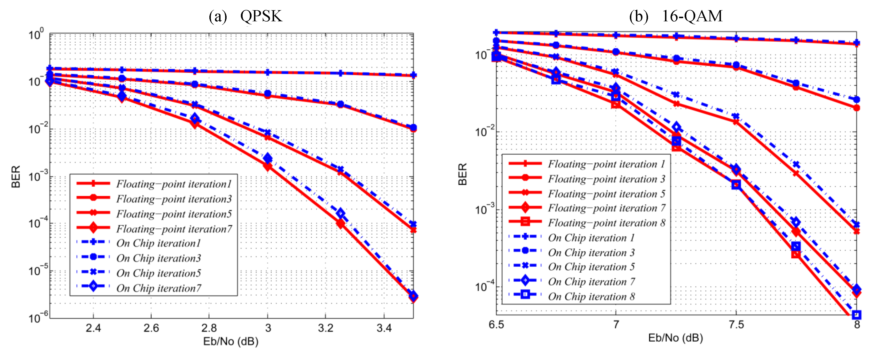
6.1. Performance Results

From all monitored signals, the outputs of the equalizer and demapper modules are exported and recorded. The saved results corresponding to all frame symbols are then compared with reference results. For all system configurations, the results acquired from the FPGA prototypes have been verified to match exactly the performance of the corresponding reference software model. Figure 16 and Figure 17 show, respectively, the receiver bit error rate (BER) performances obtained after on-chip evaluation of the designed equalizer and demapper. Furthermore, the figures show the equivalent reference software model of 1536 source bits, using 4 × 4 MIMO over a fast fading Rayleigh channel for different numbers of iterations with code rate R c = 1 2 and considering the QPSK and 16-QAM modulation schemes. The hardware-measured BER shows acceptable performance degradation when compared to floating-point C simulations.

6.2. Synthesis Results

The Xilinx ISE tool set has been used to conduct logic synthesis of the generated RTL description on FPGA. Table 1 summarizes the synthesis results of the proposed equalizer and demapper architectures. The table shows the logic utilization and maximum clock frequency when targeting a Xilinx Virtex-7 XC7VX485T FPGA. The obtained synthesis results show that a low number of slices is utilized to implement the NISC-based equalizer and demapper architectures. Furthermore, it shows that the designed equalizer can achieve a maximum operating frequency of 202.67 MHz corresponding to a minimum period of 4.93 ns. Additionally, the designed demapper can achieve a maximum operating frequency of 293 MHz corresponding to a minimum period of 3.41 ns.
Furthermore, the HDL descriptions, generated by the NISC tool set, of the proposed architectures have been synthesized on the ASIC target using the Design Compiler tool from Synopsys. Table 2 summarizes the synthesis results of the proposed architecture targeting 65-nm STMicroelectronics (ST)CMOS technology. The obtained results show that the proposed NISC-based equalizer and demapper architectures occupy a reasonable area. Furthermore, the equalizer can achieve a maximum operating frequency of 529 MHz; whereas the demapper architecture can achieve a maximum operating frequency of 520 MHz.

6.3. Throughput Results

The throughput of the proposed architectures is recorded for various system configurations. Table 3 presents the measured throughput for 2 × 2 and 4 × 4 MIMO considering block and fast fading channels at the maximum operating clock frequency. For FPGA implementation, in the case of block channel fading, 115.8 mega symbolsper second for 2 × 2 MIMO and 62.4 mega symbols per second for 4 × 4 MIMO throughputs are achieved for the FPGA implementation at an operating frequency of 202.67 MHz. In the case of fast fading, the throughput is reduced. At the same operating frequency, throughputs of 6.4 mega symbols per second and 4.7 mega symbols per second are achieved for 2 × 2 and 4 × 4 MIMO, respectively.
Furthermore, Table 3 shows the throughput of the ASIC implementation of the designed NISC-based equalizer architecture. Using the ST 65-nm CMOS technology, with the CORE65GPHVTlibrary at the nominal case operating conditions (1 V; 25 °C), the architecture can achieve a maximum throughput of 302.3 mega symbols per second in the case of MIMO 2 × 2 transmission over the block fading channel. Note that higher throughput can be achieved by using newer technologies, such as 28-nm technology and beyond. In fact, the throughput in bits per second depends on the adopted constellation. For the 16-QAM and 64-QAM modulation schemes, the designed NISC-based processor dedicated for MIMO equalization can achieve 1.2 giga bits per second and 1.8 giga bits per second, respectively. Recall that the most recent LTE-Advanced standard [4] imposes a throughput of 1 giga bit per second for the down-link and 500 mega bits per second for the up-link. Hence, for the current achieved throughput, the receiver implementing the designed application-specific processor can satisfy the requirements of throughput imposed by the LTE-Advanced standard for both constellations in the down-link and up-link.
On the other hand, Table 4 summarizes the achieved throughput of the proposed demapper design for different modulation schemes. For the FPGA implementation, the demapper architecture enables a maximum throughput of 234.6 mega LLRs per second adopting the 16-QAM modulation scheme when operating at a clock frequency of 293.242 MHz. In addition, Table 4 shows the throughput of the ASIC implementation of the designed NISC-based demapper architecture. Using the ST 65-nm CMOS technology, with the CORE65GPHVT library at nominal case operating conditions (1 V; 25 °C), the architecture can achieve a maximum throughput of 416 mega LLRs per second in the case of the 16-QAM modulation and 347 mega LLRs per second in the case of the 64-QAM modulation.

6.4. Results Comparison

6.4.1. Equalizer Module

Table 5 presents a comparison in terms of utilized resources and the performance of the proposed equalizer architecture with relevant state-of-the-art implementations, which provide complete solutions to generate estimated symbols. It is worth noting that most published works present partial implementations of MIMO equalization (for example, limited only to matrix inversion). The implementations of [24] and [25] are dedicated for 2 × 2 pre-coded and 4 × 4 spatially-multiplexed (SM) MIMO systems, respectively. In [26], a specific instruction set processor (ASIP) dedicated to MIMO MMSE-IC equalization is introduced. Compared to our proposed architecture, the ASIP architecture so-called EquASIP has identical computational resources and supports the same flexibility parameters as our design. In order to make a fair comparison, our design has been synthesized with the same target technology in the implementation being compared.
Starting with the architecture design in [25], which implements a 4 × 4 MIMO SM detector for the 802.11n standard with a throughput of 17.3 M vectors, when comparing with our work, its throughput outperforms by 3.1-times. However, this increased throughput comes at the cost of more than three-times more FPGA slices and 8.6-times more multipliers. Moreover, in contrast to our architecture, the design in [25] is not flexible for variable antenna dimensions, channel selectivity and iterative equalization.
In [24], 2 × 2 MIMO equalization includes the pre-coding stage, where the channel coefficient matrix is converted into the 4 × 4 matrix. Applying this technique using our architecture imposes more operations and, hence, lessens the computing speed of the equalization coefficients. Indeed, for the quasi-static channel, where coefficients are computed once for a data frame, the throughput is not greatly affected. The recorded throughput is 2.6-times less than that achieved by the implementation in [24], knowing that the latter uses five-times more multipliers and almost 2.5-times less FPGA registers and LUTs.
When comparing to our proposed architecture, EquASIP [26] almost requires 1.6-times more registers, 1.7-times more LUTs and 1.2-times more dedicated multipliers to be implemented. The comparison is conducted targeting the same device (Xilinx Virtex-5 LX330 FPGA) and using the same synthesis options and tools. Moreover, its throughput is less for all system configurations.

6.4.2. Demapper Module

Table 6 summarizes the comparison of the proposed demapper architecture with relevant state-of-the-art implementations in terms of utilized resources and performance. The presented demapper architectures in [27] and [28] are dedicated to certain wireless communication standards. In [27], where the conventional RTL design approach has been used, DVB-T2is the target standard; hence, the architecture design supports the QPSK, 16-QAM, 64-QAM and 256-QAM modulation schemes for non-GrayDVB constellation with rotation. Similarly, the architecture described in [28] has been designed to fulfill the requirements of the DVB-S2 standard. Four modulation schemes are supported (QPSK, 8-PSK, 16-PSK and 32-PSK) with Gray mapping constellation, as specified in [29]. Both architectures do not support iterative demodulation. In [26], an application-specific instruction set processor (ASIP) dedicated to the Max-Log-MAP demapping algorithm has been presented. The ASIP architecture, so-called DemASIP, provides full flexibility and can be utilized in multiple wireless communication standards (WiFi, WiMax, LTE and DVB) with the support of iterative demodulation. Compared to our proposed architecture, DemASIP has the same computational units and supports the same flexibility parameters as our design. To compare fairly, our proposed architecture design has been synthesized with the same target technology used in the implementation being compared.
When comparing to our proposed architecture, the demapper architecture in [27] almost requires 3.33-times more dedicated multipliers, 3.1-times more LUTs, but 2.2-times less registers to be implemented. Whatever the modulation type is, the demapping of one symbol lasts for 10 clock cycles with a maximum reached frequency of 62 MHz. In contrast, the number of required clock cycles to demap one symbol varies according to the modulation scheme in our proposed architecture. For the selected device, our proposed demapper can operate 3.1-times faster, and it outperforms the described design in [27] when adopting QPSK, 16-QAM and 64-QAM modulation modes. In case of 256-QAM, the latter design provides better throughput. In fact, the demapper architecture in [27] exploits demapping metric level parallelism. It can calculate nine Euclidean distances in parallel by using nine computational units; hence, high throughput is achieved in the case of high-order modulation schemes. Whereas in the case of lower modulation schemes, the computational units are not fully exploited to perform the computations related to one received symbol.
In [28], the timing information about the hardware implementation is not available. Only device utilization is presented. Although the architecture is optimized targeting the M-PSK modulation schemes for Gray mapping constellation, the presented logic utilization summary reveals the need of 1.8-times more logic devices and 2.67-times more multipliers compared to our proposed demapper design.
Regarding DemASIP [26], although it has a tailored instruction set, the architecture design has to integrate an instruction decoder. The comparison is conducted targeting the same device (Xilinx Virtex-5 LX330 FPGA) and using the same synthesis options and tools. From the implementation view, DemASIP almost requires 1.44-times more slice registers and 2.1-times more slice LUTs compared to our proposed demapper architecture. In addition, the critical path of DemASIP includes 24 levels of combinational logic, and it is related to the fetch program counter register. DemASIP can achieve a maximum operating frequency of 186 MHz; whereas the proposed architecture can achieve a maximum operating frequency of 240 MHz and, thus, it is 1.29-times faster than DemASIP. On the other hand, fetching and decoding the instructions impose additional pipeline stages. As shown in Table 6, the proposed demapper architecture achieves better throughput than DemASIP in all system configurations and all combinations of mapping styles, modulation types and SSD.
In both designed NISC-based architectures, the comparison results in terms of performance and implementation area confirm the feasibility of adopting the proposed design and prototyping flow. This approach combines the conventional NISC tool set flow and direct controlling of hardware resources to ensure both productivity and implementation efficiency, in designing flexible, yet efficient application-specific processors in the application domain of digital communications.

7. Conclusions

The development and prototyping flow of NISC-based architectures dedicated to MMSE turbo equalization and Max-Log-MAP turbo demapping have been presented. The described designs are efficient, flexible and support different communication modes defined in the WiFi, WiMAX, DVB-RCS, LTE and LTE-Advanced wireless communication standards. The proposed designing flow is detailed starting from architecture specification till FPGA implementation. Using this flow, the NISC-based architectures of the equalizer and demapper are prototyped targeting the Xilinx Virtex-7 XC7VX485T. The proper functionality of both architectures has been verified, and their corresponding performances have been evaluated for different system configurations by conduction on-chip validation. The FPGA prototype of the proposed equalizer architecture achieves a throughput of 115.8 mega symbols per second for 2 × 2 and 62.4 mega symbols per second for 4 × 4 spatially-multiplexed (SM) MIMO systems when operating at a clock frequency of 202.67 MHz. Moreover, the FPGA prototype of the proposed demapper architecture enables a maximum throughput of 234.6 mega LLRs per second adopting the 16-QAM modulation scheme when operating at a clock frequency of 293.242 MHz. The two proposed architectures are compared to relevant state-of-the-art implementations. The comparison results illustrate the effectiveness of the proposed design approach, which allows shortening development cycles, while ensuring high implementation efficiency.

Acknowledgments

This work is done in collaboration between Telecom Bretagne and Lebanese University, and funded by the Electronics Department of Telecom Bretagne.

Author Contributions

M. Rizk developed the design and prototyping flow, designed and implemented the architectures, and wrote the paper. A. Baghdadi scientifically supervised the work, contributed in implementing the architectures, and participated in writing the paper. M. Jezequel, Y. Mohanna, and Y. Atat academically supervised the work for Telecom Bretagne and Lebanese University.

Conflicts of Interest

The authors declare no conflict of interest.

References

  1. Digital Video Broadcasting (DVB); Interaction Channel for Satellite Distribution Systems. ETSI EN 301 790 V1.5.1. 2009. Available online: http://www.etsi.org/deliver/etsi_en/301700_301799/301790/01.05.01_60/en_301790v010501p.pdf (accessed on 23 August 2016).
  2. IEEE Draft Standard; Part 11: Wireless LAN Medium Access Control (MAC) and Physical Layer (PHY) Specifications; Amendment 4: Enhancements for Higher Throughput; IEEE Std 802.11; March 2012; Available online: http://standards.ieee.org/getieee802/download/802.11-2012.pdf (accessed on 23 August 2016).
  3. 802.16 IEEE Standard for Local and Metropolitan Area Networks, Part 16: Air Interface for Fixed Broadband Wireless Access Systems. 802.16-2004. 2004. Available online: http://ieeexplore.ieee.org/document/1350465 (accessed on 23 August 2016).
  4. 3GPP Technical Specifications 36.212, Multiplexing and Channel Coding (Release 11). ETSI TS 136 212 V12.2.0. 2014. Available online: http://www.etsi.org/deliver/etsi_ts/136200_136299/136212/12.02.00_60/ts_136212v120200p.pdf (accessed on 23 August 2016).
  5. Douillard, C.; Jézéquel, M.; Berrou, C.; Picart, A.; Didier, P.; Glavieux, A. Iterative correction of inter symbol interference: Turbo equalization. Eur. Trans. Telecommun. ETT 1995, 6, 507–511. [Google Scholar] [CrossRef]
  6. Laot, C.; Le Bidan, R.; Leroux, D. Low-complexity MMSE turbo equalization: A possible solution for EDGE. IEEE Trans. Wirel. Commun. 2005, 4, 965–974. [Google Scholar] [CrossRef]
  7. Berrou, C. Codes and Turbo Codes; Springer: Paris, France, 2010. [Google Scholar]
  8. Gamba, M.T.; Masera, G.; Baghdadi, A. Iterative MIMO detection: Flexibility and convergence analysis of SISO list sphere decoding and linear MMSE detection. In Proceedings of the International Conference on Software, Telecommunications and Computer Networks (SoftCOM), Dalmatia, Croatia, 23–25 September 2010; pp. 175–179.
  9. Reynolds, D.; Wang, X. Low-complexity turbo-equalization for diversity channels. Signal Process. 2001, 81, 989–995. [Google Scholar] [CrossRef]
  10. Li, X.; Ritcey, J. Bit-interleaved coded modulation with iterative decoding. IEEE Commun. Lett. 1997, 1, 169–171. [Google Scholar]
  11. Abdel Nour, C.; Douillard, C. Improving BICM performance of QAM constellations for broadcasting applications. In Proceedings of the International Symposium on Turbo Codes and Related Topics (ISTC), Lausanne, Switzerland, 1–5 September 2008; pp. 55–60.
  12. Robertson, P.; Hoeher, P.; Villebrun, E. Optimal and sub-optimal Maximum A Posteriori algorithms suitable for turbo decoding. Eur. Trans. Telecommun. ETT 1997, 8, 119–125. [Google Scholar] [CrossRef]
  13. Rizk, M.; Baghdadi, A.; Jezequel, M.; Mohanna, Y.; Atat, Y. Flexible and efficient architecture design for MIMO MMSE-IC linear turbo-equalization. In Proceedings of the IEEE International Conference on Communications and Information Technology (ICCIT), Porto, Portugal, 19–21 June 2013; pp. 340–344.
  14. Rizk, M.; Baghdadi, A.; Jezequel, M.; Mohanna, Y.; Atat, Y. Nisc-based soft-input soft-output demapper. IEEE Trans. Circuits Syst. II 2015, 62, 1098–1102. [Google Scholar] [CrossRef]
  15. Osseiran, A.; Boccardi, F.; Braun, V.; Kusume, K.; Marsch, P.; Maternia, M.; Queseth, O.; Schellmann, M.; Schotten, H.; Taoka, H.; et al. Scenarios for 5G mobile and wireless communications: The vision of the METIS project. IEEE Commun. Mag. 2014, 52, 26–35. [Google Scholar] [CrossRef]
  16. Menard, D.; Serizel, R.; Rocher, R.; Sentieys, O. Accuracy Constraint Determination in Fixed-Point System Design. EURASIP J. Embed. Syst. 2008. [Google Scholar] [CrossRef]
  17. Rizk, M.; Baghdadi, A.; Jézéquel, M.; Mohanna, Y.; Atat, Y. Quantization and fixed-point arithmetic for MIMO MMSE-IC linear turbo-equalization. In Proceedings of the IEEE International Conference on Microelectronics, (ICM), Beirut, Lebanon, 15–18 December 2013; pp. 1–4.
  18. Bigdeli, A.; Biglari-Abhari, M.; Salcic, Z.; Tin Lai, Y. A new pipelined systolic array-based architecture for matrix inversion in FPGAs with Kalman filter case study. EURASIP J. Appl. Signal Process. 2006. [Google Scholar] [CrossRef] [PubMed]
  19. NISC Toolset Website. Available online: http://www.ics.uci.edu/nisc/ (accessed on 15 November 2014).
  20. Gorjiara, B.; Gajski, D.; Reshadi, M. Gnr: A formal language for specification, compilation, and synthesis of custom embedded processors. In Processor Description Languages: Applications and Methodologies; Mishra, P., Dutt, N., Eds.; Morgan Kaufmann Publishers: Boston, MA, USA, 2008; Charpter 13. [Google Scholar]
  21. Gorjiara, B.; Reshadi, M.; Gajski, D. Generic architecture description for retargetable compilation and synthesis of application-specific pipelined IPs. In Proceedings of the IEEE International Conference on Computer Design (ICCD), San Jose, CA, USA, 1–4 October 2006; pp. 356–361.
  22. Reshadi, M.; Gajski, D. Interrupt and low-level programming support for expanding the application domain of statically-scheduled horizontal-microcoded architectures in embedded systems. In Proceedings of the IEEE Design, Automation and Test in Europe Conference and Exhibition (DATE), Nice, France, 16–20 April 2007; pp. 1–6.
  23. Xilinx. ChipScope Pro 10.1 Software and Cores User Guide. Available online: http://www.xilinx.com/ise/verification/chipscope_pro_sw_cores_10_1_ug029.pdf (accessed on 23 August 2016).
  24. Karakolah, D. Conception et Prototypage d’un Récepteur Itératif Pour des Systèmes de Transmision MIMO Avec Précodage Linéaire. Ph.D. Dissertation, Department of Electronics, Telecom Bretagne, Brest, France, 2009. [Google Scholar]
  25. Kim, H.; Zhu, W.; Bhatia, J.; Mohammad, K.; Shah, A.; Danesrad, B. A Practical Hardware Friendly MMSE Detector for MIMO-ODFM-Based Systems. EURASIP J. Adv. Signal Process. 2008. [Google Scholar] [CrossRef]
  26. Jafri, A.R. Architectures Multi-ASIP Pour Turbo Récepteur Flexible. Ph.D. Dissertation, Department of Electronics, Telecom Bretagne, Brest, France, 2011. [Google Scholar]
  27. Li, M. Design, Imlementation, and Prototyping of an Iterative Receiver for Bit-Interleaved Coded Modulation System Dedicated to DVB-T2. Ph.D. Dissertation, Department of Electronics, Telecom Bretagne, Brest, France, 2012. [Google Scholar]
  28. Park, J.W.; Sunwoo, M.H.; Kim, P.S.; Chang, D.-I. Low complexity soft-decision demapper for high order modulation of DVB-S2 system. In Proceedings of the IEEE International SoC Design Conference (ISOCC), Busan, Korea, 24–25 November 2008; Volume 02, pp. II-37–II-40.
  29. Digital Video Broadcasting (DVB); User Guidelines for the Second Generation System for Broadcasting, Interactive Services, News Gathering and Other Broad-Band Satellite Applications (DVB-S2). ETSI TR 102 376 V1.1.1. 2005. Available online: http://www.etsi.org/deliver/etsi_tr/102300_102399/102376/01.01.01_60/tr_102376v010101p.pdf (accessed on 23 August 2016).
Figure 1. Block diagram of the MIMO-OFDM turbo receiver.
Electronics 05 00050 g001
Figure 2. Transition from the application-specific instruction set processor (ASIP) to the no instruction set computer (NISC) design approach.
Electronics 05 00050 g002
Figure 3. Proposed equalizer architecture.
Electronics 05 00050 g003
Figure 4. Proposed NISC-based demapper architecture.
Electronics 05 00050 g004
Figure 5. (a) Minimum finder operational unit; (b) subtractor used in the subtraction operation of the minimum pair.
Electronics 05 00050 g005
Figure 6. NISC tool set generic design flow.
Electronics 05 00050 g006
Figure 7. Adopted design flow.
Electronics 05 00050 g007
Figure 8. “MinFinder” module generic netlist representation (GNR) hierarchical description.
Electronics 05 00050 g008
Figure 9. Pre-bound function sample that merges multiple operations.
Electronics 05 00050 g009
Figure 10. (a) List of C definitions related to pre-bound functions defining the functionality of the DemaNISC module and (b) GNR description of the pre-bound function “QPSK1”, which declares the control values that should be applied at the first step of demapping for QPSK modulation scheme.
Electronics 05 00050 g010
Figure 11. Xilinx ISE simulation window showing equalizer architecture output signals.
Electronics 05 00050 g011
Figure 12. 1 x LUT structure.
Electronics 05 00050 g012
Figure 13. NISC-based MMSE MIMO turbo equalizer architecture on-chip prototype.
Electronics 05 00050 g013
Figure 14. ChipScope Pro Analyzer software waveform window.
Electronics 05 00050 g014
Figure 15. NISC-based demapper architecture on-chip prototype.
Electronics 05 00050 g015
Figure 16. Comparison between the simulated reference BER and measured BER after on-chip evaluation of the designed equalizer for 1536 source bits, a 1 2 code rate, 4 × 4 MIMO and a fast fading Rayleigh channel.
Electronics 05 00050 g016
Figure 17. Comparison between the simulated reference BER and measured BER after on-chip evaluation of the designed demapper for for 1536 source bits, a 1 2 code rate, 4 × 4 MIMO and fast fading Rayleigh channel.
Electronics 05 00050 g017
Table 1. FPGA synthesis results of the proposed NISC-based equalizer and demapper architectures targeting Xilinx Virtex-7 XC7VX485T.
Logic Utilization and TimingEqualizerDemapper
Slice Registers2029 out of 607,2001290 out of 607,200
Slice LUTs5942 out of 303,6001517 out of 303,600
DSP48Es12 out of 28006 out of 2800
Max Clock Frequency202.67 MHz293 MHz
Table 2. Application-specific integrated circuit (ASIC) synthesis results of the proposed NISC-based equalizer and demapper architectures targeting 65-nm STCMOS technology.
Logic Utilization and TimingEqualizerDemapper
Operating conditionsnominal case (1 V; 25 °C)
Area0.126 mm20.048 mm2
Maximum operating frequency529 MHz520 MHz
Table 3. Throughput of the proposed NISC-based equalizer architecture. SM, spatially-multiplexed.
ImplementationFading TypeThroughput (Mega Symbols per Second)
2 × 2 MIMO SM4 × 4 MIMO SM
FPGA @202.67 MHzBlock fading115.862.4
Fast fading6.44.7
ASIC @ 529 MHzBlock fading302.3162.8
Fast fading16.812.2
Table 4. Throughput results of the proposed NISC-based demapper architecture.
Modulation TypeThroughput (Mega LLRsper Second)
FPGA @ 293 MHzASIC @ 520 MHz
QPSK195.5347
16-QAM234.6416
64-QAM195.5347
256-QAM138244.7
Table 5. Comparison summary of the proposed equalizer with relevant state-of-the-art implementations.
System ConfigurationReferenceTarget DeviceOperating Frequency (MHz)FPGA ResourcesClock CyclesThroughput (mega Operations per Second)
RegistersLUTDedicated Multipliers
2 × 2 SM[25]Virtex-II1401416610338817.31
Block FadingThis work914604127845.57
4 × 4 SM[26]Virtex-V130317411299141310
Block FadingThis work14620296536121311.23
4 × 4 SM[26]Virtex-V130317411299142340.56
Fast FadingThis work14620296536121730.84
2 × 2[24]Virtex-V608172715601120
Precodin Quasi-StaticgThis work14620296536123.2545
2 × 2 SM[26]Virtex-V13031741129914891.46
Fast FadingThis work1462029653612632.32
2 × 2 SM[26]Virtex-V13031741129914816.25
Block FadingThis work1462029653612720.86
Table 6. Comparison summary of the proposed demapper with the relevant state-of-the-art implementations. SSD, signal space diversity.
Mapping Style and SSDReferenceIterative/Non-Iterative DemappingTarget DeviceOperating Frequency (MHz)FPGA ResourcesModulation TypeClock CyclesThroughput (mega LLR per Second)
RegistersLUTDedicated Multipliers
non-Gray with SSD[27]non-iterativeVirtex II Pro XC2VP362791466720QPSK1012.4
16-QAM24.8
64-QAM37.2
256-QAM49.6
This workiterative and non-iterative194174015236QPSK577.45
16-QAM1077.45
64-QAM2644.68
256-QAM8218.89
[26]iterative and non-iterativeVirtex5 XC5VLX33018619183201664-QAM2741.33
256-QAM8317.93
This work24013281524664-QAM2655.27
256-QAM8223.37
Gray without SSD[28]non-iterativeVirtex II XC2-V6000-182616QPSK, 8-PSK--
16-APSK, 32-APSK--
This workiterative and non-iterative16010056QPSK480.13
8-PSK953.42
16-APSK1737.71
32-APSK3324.28
[26]iterative and non-iterativeVirtex-V XC5VLX330186191832016QPSK493
16-QAM6124
64-QAM10111.6
256-QAM1882.67
This work240132815246QPSK3159.67
16-QAM5191.6
64-QAM9159.67
256-QAM17112.71
non-Gray without SSD[26]non-iterativeVirtex-V XC5VLX330186191832016QPSK662
8-PSK1055.8
16-QAM,16-APSK1841.33
32-APSK3427.35
64-QAM6616.91
256-QAM2585.77
This work240132815246QPSK595.8
8-PSK979.83
16-QAM,16-APSK1756.35
32-APSK3336.29
64-QAM6522.1
256-QAM2577.46

