Review

Recent Progress in Source/Drain Ohmic Contact with β-Ga2O3

1
College of Electronic and Electrical Engineering, Henan Normal University, No. 46 East of Construction Road, Xinxiang 453007, China
2
College of Intelligent Engineering, Henan Institute of Technology, No. 699 Pingyuan Road (East Section), Xinxiang 453003, China
3
State Key Laboratory of ASIC and System, School of Microelectronics, Fudan University, No. 220 Han Dan Road, Shanghai 200433, China
*
Authors to whom correspondence should be addressed.
Inorganics 2023, 11(10), 397; https://doi.org/10.3390/inorganics11100397
Submission received: 31 August 2023 / Revised: 29 September 2023 / Accepted: 4 October 2023 / Published: 11 October 2023
(This article belongs to the Special Issue Advanced Inorganic Semiconductor Materials)

Abstract

:
β-Ga2O3, with excellent bandgap, breakdown field, and thermal stability properties, is considered to be one of the most promising candidates for power devices including field-effect transistors (FETs) and for other applications such as Schottky barrier diodes (SBDs) and solar-blind ultraviolet photodetectors. Ohmic contact is one of the key steps in the β-Ga2O3 device fabrication process for power applications. Ohmic contact techniques have been developed in recent years, and they are summarized in this review. First, the basic theory of metal–semiconductor contact is introduced. After that, the representative literature related to Ohmic contact with β-Ga2O3 is summarized and analyzed, including the electrical properties, interface microstructure, Ohmic contact formation mechanism, and contact reliability. In addition, the promising alternative schemes, including novel annealing techniques and Au-free contact materials, which are compatible with the CMOS process, are discussed. This review will help our theoretical understanding of Ohmic contact in β-Ga2O3 devices as well as the development trends of Ohmic contact schemes.

Graphical Abstract

1. Introduction

Si-based devices are the dominant devices used for power applications. However, with the increasing demand for much faster and more convenient network communication, Si-based device techniques cannot meet these requirements due to their physical properties. Thus, new-material devices should be investigated for operating at high temperatures, at high power, and in harsh environments. In recent years, wide-bandgap semiconductors including GaN (3.4 eV) and SiC (3.25 eV) have been developed, and they have replaced Si-based techniques in many fields due to their advantages in terms of their material properties [1,2,3,4,5]. Recently, β-Ga2O3, which is mostly thermally and chemically stable in five polymorphs [6,7,8], has attracted more and more attention for power applications because β-Ga2O3 has a wide bandgap of 4.6–4.9 eV and a breakdown field strength as high as 8 MV/cm [9,10,11]. In addition, for the Baliga figure and Johnson’s figure of merit, when evaluating its application potential in power devices, β-Ga2O3 exhibits the best performance [9,10,11]. The basic physical properties and figures of merit (FOM) of commonly used semiconductor materials are shown in Table 1. For this reason, researchers have obtained plenty of results related to β-Ga2O3-based FETs [12,13,14], SBDs [15,16,17,18], and solar-blind ultraviolet photodetectors [19,20,21]. In 2023, Wang et al. [13] demonstrated a metal–heterojunction composite field-effect transistor that exhibited a breakdown voltage (BV) of around 2160 V. In addition, the corresponding RON,SP was 6.35 mΩ·cm2. So far, the power figure of merit (P-FOM) achieved the highest value of 0.73 GW/cm2 for e-mode β-Ga2O3 devices. For SBDs, Hao et al. [17] used an optimized p-type NiO (with a hole concentration of 1017 cm−3) junction-termination extension (JTE) technique that exhibited a BV and RON,SP of 2.11 kV and 2.9 mΩ·cm2, respectively. For this reason, the P-FOM was as high as 1.54 GW/cm2. For the junction barrier Schottky (JBS) diode, Wu et al. [18] fabricated a device with a well-designed field plate to suppress the crowding effect of the electric field. The forward current and BV could reach 5.1 A and 1060 V, respectively. At the circuit level, the hybrid circuit exhibited more efficiency compared with the Si-based one. An RON-BV benchmark comparison of β-Ga2O3-based devices with other published results was also presented in their work. The RON-BV characteristics for β-Ga2O3-based devices were comparable with GaN-based ones [22]. To fully exploit β-Ga2O3‘s potential in power electronics applications, the material quality, device structure, and process details should be further optimized. By embedding indium tin oxide (ITO) electrodes, Zhang et al. [19] fabricated a fully transparent MSM-structured solar-blind UV photodetector with an excellent dark current, normalized photocurrent-to-dark-current ratio (NPDR), responsivity, rejection ratio, and specific detectivity characteristics. Another advantage of β-Ga2O3 material is that single large β-Ga2O3 crystals can be cost-effectively mass produced using melt–growth methods, such as EFG [23], FZ [24,25], VB [26,27], and CZ [28,29] methods. Additionally, a high-quality β-Ga2O3 epilayer can be realized using MOCVD [30,31], MBE [32,33], HVPE [34,35], and MOVPE [36,37] methods to form a well-controlled n-type doping using Si, Ge, and Sn. However, the p-type doping technique is still challenging because the activation energy of the acceptors and the self-trapping energy of the holes are large [38,39]. For the purpose of achieving p-type Ga2O3, great efforts have been taken by researchers from all over the world [40,41,42,43,44,45,46,47,48,49,50,51].
For power applications, Ohmic contact is one of the key steps in β-Ga2O3 device fabrication processes. Ohmic contact resistance (RC), specific contact resistance (ρc), and thermal stability are important indexes of contact quality. A lower RC can reduce voltage drop across the contact region and power loss. For GaN-based devices, Au-free low-temperature Ohmic contact techniques are proposed to realize CMOS-compatible and gate-first techniques [52,53]. Until now, because of the wide-bandgap property of β-Ga2O3 and Fermi-level pinning [54,55,56], Ohmic contact methods for Ga2O3-based devices have remained challenging. The metal schemes, annealing conditions (the annealing temperature, durations, and atmosphere), and doping concentration of Ga2O3 have been investigated and optimized to obtain low-RC contact. In this review, we will first give a brief introduction of metal–semiconductor contact theory. After that, the state-of-the-art advances in Ohmic contact techniques for β-Ga2O3 will be presented and discussed, including metal electrodes, surface treatments, ion implantation, epitaxial regrowth, and adding an interlayer. Finally, we will give some perspectives for further studies on Ohmic contact with β-Ga2O3 in the future.

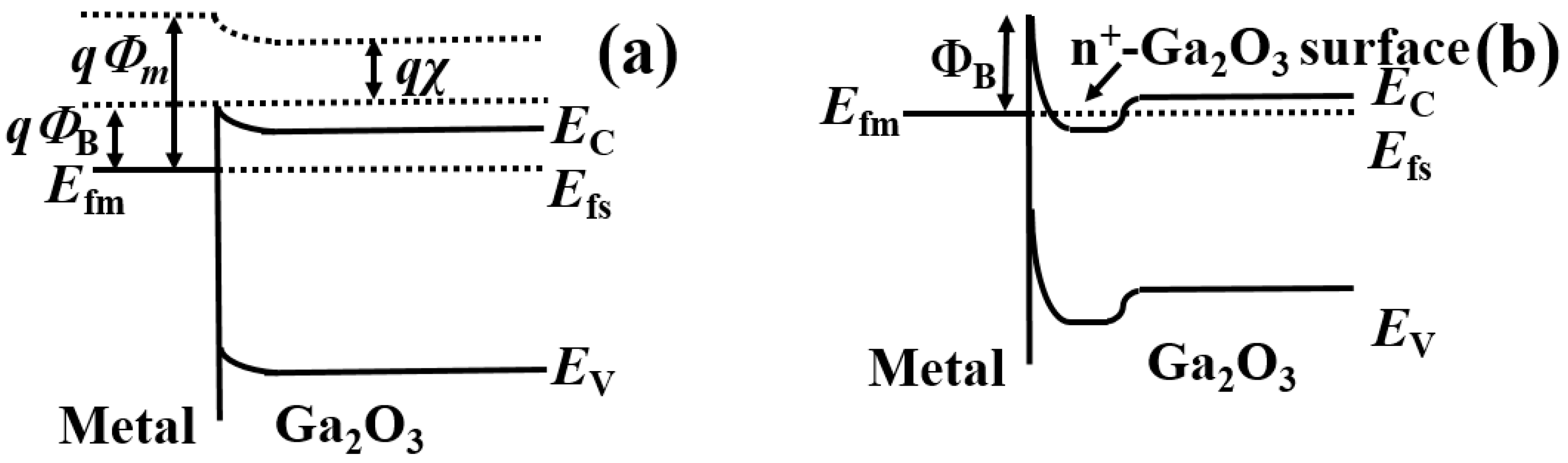
2. Basic Metal–Ga2O3 Contact Physical Theory

Metal–semiconductor contact is a critical part of β-Ga2O3 power devices. A device’s performance is mainly limited by the Ohmic contact property. Two types of contacts (Schottky and Ohmic) can be formed due to the differences in the work functions of contact metals [57,58,59]. For wide-bandgap β-Ga2O3, the contacts always exhibit Schottky behavior. When metal and Ga2O3 come into contact, the energy band of the Ga2O3 side bends up to make their Fermi levels equal. As shown in Figure 1a, the Schottky barrier height from the metal side (ΦB) can be described as
ΦB = Φmχ,
where χ represents the semiconductor’s electron affinity (4 eV for Ga2O3 in our case [60]) and Φm represents the metal work function. Therefore, it is desirable to select a metal with a Φm lower than 4 eV to realize a negative ΦB, which allows electrons to flow freely across it to form an Ohmic contact. Unfortunately, the lack of suitable metal materials with lower work functions makes Ohmic contact formation challenging. Generally, researchers have proposed Ohmic contact schemes to form a lower ΦB or an n+-doped Ga2O3 region for electron tunneling. When a semiconductor is heavily doped (ND > 1018 cm−3), field emission (FE) dominates the electron tunneling [61,62]. In order to obtain a low RC or ρc, a higher ND is expected.
The Ohmic contact resistance (RC, measured in Ω·mm) and specific contact resistance (ρc, measured in Ω·cm−2) are always determined using the transmission line model (TLM) method [63,64]. Details concerning the TLM measurement technique can be seen in the references mentioned above.
The metal work function, metal schemes, interfacial reactions between metal and a semiconductor during the annealing process, and the doping concentration of Ga2O3 in the source/drain region are significant influencing factors for the Ohmic contact property. Until now, researchers from universities and research institutes have proposed Ohmic contact schemes involving optimizing the metal materials, annealing condition, source/drain doping method and concentration, and source/drain etching as well as adding an interlayer in the source/drain region.

3. Approaches to Metal–Ga2O3 Ohmic Contact

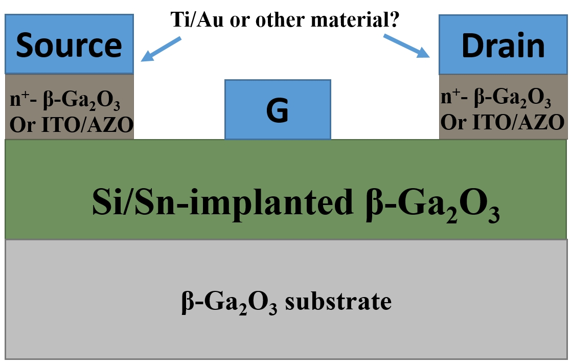
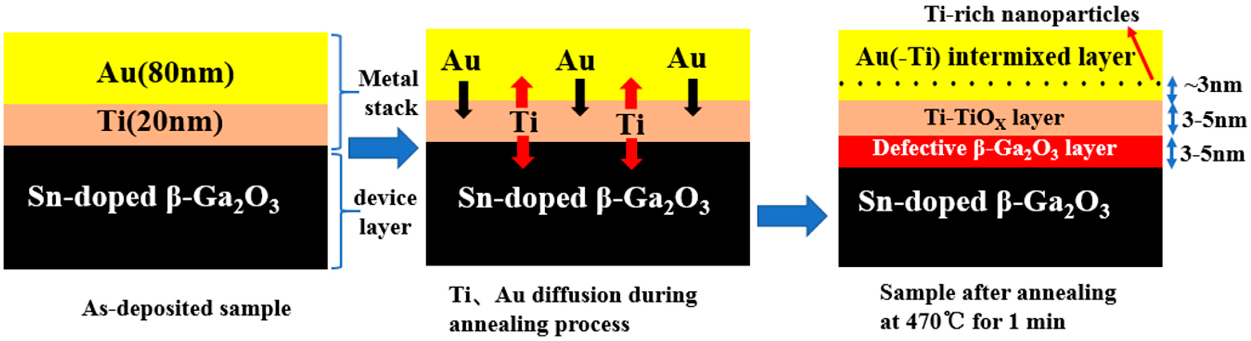
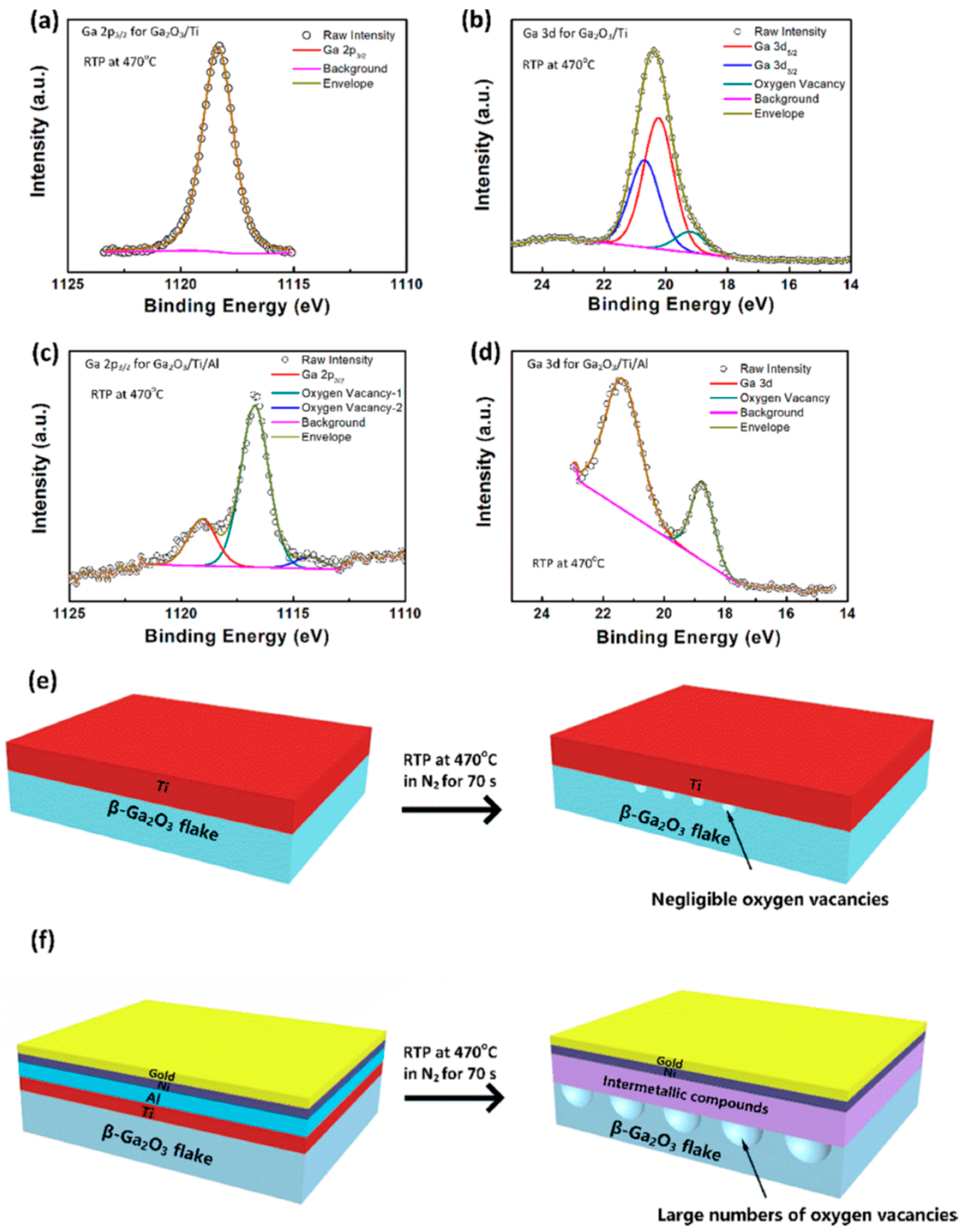
3.1. Metal Electrode

From the metal–semiconductor contact theory, the work function of the selected metal material crucially affects the Ohmic contact quality. Thus, in the early period, Yao et al. [65] investigated the Ohmic contact properties and surface morphologies of nine metal materials, including Ti, In, Ag, Sn, W, Mo, Sc, Zn, and Zr with Sn-doped ( 2 ¯ 01) β-Ga2O3. From their results, the work function is not the main factor influencing the contact quality. Sc, with the lowest work function, cannot form Ohmic contacts under different annealing conditions. Ti/Au metal schemes with a 400 °C annealing process exhibited the lowest RC values. Cross-sectional transmission electron microscopy (TEM) and energy-dispersive X-ray spectroscopy (EDX) mapping showed that Ga and O diffused into the Ti layer during the annealing process. They concluded that interfacial reactions during the annealing process played a crucial part in Ohmic contact formation. Otherwise, the ultra-wide bandgap property leads to a pinning effect due to defects and surface states that lie in the mid-gap, which are not beneficial for forming an Ohmic contact.
Other groups have reported Mg/Au and Cr/Au metal schemes for Ohmic contact formation [66,67]. In the Mg (3.66 eV)/Au method, the ρc of 2.2 × 10⁻⁴~2.1 × 10⁻⁵ Ω·cm−2 was achieved with an annealing process at temperatures varying from 300 °C to 500 °C. Until now, the most common metallization schemes of Ohmic contact for β-Ga2O3 have used Ti/Au. Ti is used as an adhesion layer with a low work function. Au serves as a cap layer to prevent the oxidation of metal stacks during the high-temperature process. For the purpose of understanding the mechanism, Lee et al. [68] deposited Ti/Au (20/80 nm) on a Sn-doped β-Ga2O3 (010) substrate and carried out a 470 °C rapid thermal annealing (RTA) process for 1 min to form an Ohmic contact. Scanning transmission electron microscopy (STEM), high-resolution transmission electron microscopy (HRTEM), and EDX measurements were taken to understand the interfacial reactions and components. They found that a defective β-Ga2O3 layer (3–5 nm), a Ti–TiOx layer (3–5 nm), and an intermixed Au–Ti layer containing Ti-rich nanocrystalline inclusions were formed sequentially, as shown in Figure 2. They deduced that the Ti–TiOx layer (3–5 nm) with a small bandgap could provide an efficient path for the electron flow. In addition, the lattice matching between the defective β-Ga2O3 layer and the β-Ga2O3 substrate could enhance the carrier mobility by reducing the collision probability, resulting in a lower RC. Before this work, Higashiwaki et al. [69] showed TEM results for an interface and deduced that interface reactions help improve contact quality.
Also, multilayer metal contact schemes were proposed for obtaining lower RC values, such as Ti/Al/Au [70,71], Ti/Al/Ni/Au [72,73], and Ti/Au/Ni [32,33]. As can be seen in Figure 3, Krishnamoorthy et al. formed a δ-doped β-Ga2O3 structure in the source/drain region to form a heavily doped contact area. After Ti/Au/Ni deposition, a 470 °C RTA process was employed for 1 min for Ohmic contact formation. The extracted RC and ρc were 0.35 Ω·mm and 4.3 × 10⁻⁶ Ω·cm−2, respectively. In addition, the fabricated β-Ga2O3 FET exhibited excellent ID and gm results. By using Ti/Al/Au contact metals, Zhou et al. [71] achieved a low RC of 0.75 Ω·mm by adopting a highly Sn-doped channel. For AlGaN/GaN HEMT, Ti/Al/Ni/Au is one of the most mature metal schemes for Ohmic contact formation [74,75]. For β-Ga2O3 devices, Chen et al. [73] deposited Ti/Al/Ni/Au multilayer metal stacks and carried out an RTA process with the temperature at 470 °C for 70 s. By analyzing the X-ray photoelectron spectroscopy (XPS) results, as shown in Figure 4, they concluded that the use of Al can lead to the formation of a Ti–Al phase with a low work function, which is beneficial for oxygen vacancy generation at the interface. In n-type β-Ga2O3, the vacancies act as donors, enhancing the electron flow and realized Ohmic contact.
In 2022, Tetzner et al. [76] used a TiW alloy instead of the traditional Ti/Au metal schemes, and a low ρc of 1.5 × 10⁻⁵ Ω·cm−2 was extracted after a 700 °C RTA process. The temperature was 200 °C higher than that of the Ti/Au schemes. To understand the Ohmic contact formation mechanism, STEM HAADF and EDX were employed. The STEM HAADF image showed that a 3–5 nm TiOX interlayer was formed, which was confirmed with the STEM EDX. They suspected that vacancies, defects, or Ga impurities that exist in the interlayer are beneficial for electrons flowing freely to reduce the RC.
Thermal stability is another important index of contact quality. For Ti/Au electrodes, the most commonly used annealing temperatures are between 400 °C to 500 °C. Above 500 °C, Yao et al. [65] found that the Ohmic contacts degraded in their results. In 2022, Lee et al. [77] systematically investigated the influence of temperature on Ohmic contact quality. In their results, when the annealing temperature increased from 470 °C to 520 °C, aggressive Au diffused into the interface and reacted with Ga that diffused out, resulting in a much thicker Ti–TiOx layer due to GaAu2 formation, which accounted for the contact degradation. In Kim’s [78] results, the RC increased when the temperature changed from 400 °C to 500 °C or 600 °C. They deduced that this could have been due to an increased amount of Ti oxide. Related investigations have also been conducted and reported [79,80,81]. Therefore, more research into interfacial reactions for Ti/Au schemes and alternative metallization schemes, including Au-free electrodes, should be proposed to solve the instability issue of the Ti/β-Ga2O3 interface using Ti/Au metal schemes. It should be noted that excellent Ohmic contact cannot be achieved just by selecting metal materials. Combined with other techniques, including surface treatment, ion implantation, epitaxial regrowth, adding an interlayer, etc., the contact quality can be improved and optimized.

3.2. Surface Treatment

A surface treatment before metal deposition can also help improve the Ohmic contact property (dry etching, plasma bombardment, etc.). In 2012, Higashiwaki et al. [82] compared the I–V results of Ga2O3 devices with and without the RIE treatment. The RIE process was implemented by using a BCl3/Ar mixing gas for 1 min before Ti/Au (20/230 nm) deposition. The samples with the RIE treatment exhibited Ohmic contact characteristics, while without the RIE process the samples showed Schottky contact features. They speculated that the Ohmic contact formation was due to the large number of oxygen-vacancy surface defects formed during the RIE process. The defects acted as donors for Ohmic contact realization. Combined with Si ion implantation [83], they achieved a ρc of 4.6 × 10⁻⁶ Ω·cm−2 with a doping concentration of 5 × 1019 cm−3. In addition, Zhou et al. [70] performed an Ar plasma bombardment process and optimized the duration of 30 s for generating oxygen vacancies, which are good for n-type surface doping. The mechanism was similar to that of the BCl3/Ar RIE process. The RC values in their results were as low as 0.95 Ω·mm. Related results have also been reported by other groups [33,69,71,84,85,86].
Also, the annealing temperature and atmosphere may affect the interfacial reactions that dominate Ohmic contact formation. Bae et al. [87] compared the electrical results of the fabricated β-Ga2O3 nanobelts under different atmospheres with various temperatures. The samples treated under a N2 atmosphere exhibited better characteristics that the ones treated in an air environment. Under an Ar atmosphere, Li et al. [88] reduced the RC to 0.387 Ω·mm by optimizing the annealing temperature and the durations. In their results, a large drain current density of ~3.1 mA/μm (Vds = 100 V) was achieved due to the low RC. To fully understand the influence of an Ar atmosphere on improving the β-Ga2O3 device’s I–V characteristics, XPS was used to show the material changes during the RTA process. From the results, as can be seen in Figure 5, they deduced that Ti reduced β-Ga2O3 and generated large numbers of oxygen vacancies at the interface during the annealing process, which served as effective electron donors. For this reason, the depletion layer was narrower, resulting in Ohmic behavior and a low RC for β-Ga2O3 FETs. The annealing temperature is another element that affects the interface reactions to determine the Ohmic contact property. In 2022, Lee et al. [77] systematically investigated the influence of temperature (from 370 °C to 520 °C) on the Ohmic contact property. The lowest RC occurred when temperature was 420 °C. When the temperature increased, the RC increased as well. To investigate the reason for the degradation of the RC with an increasing temperature, cross-sectional S/TEM was employed for a sample with an annealing temperature of 520 °C. Their results show that the thickness of the Ti-TiOx layer (25–30 nm) increased due to the formation of GaAu2 inclusions, which was caused by Au aggressively diffusing in and its reaction with Ga that had diffused out. In their early results [68], a thin Ti–TiOx layer was beneficial for electron transport. The degradation of contact quality was the result of the increasing Ti–TiOx layer thickness. Also, in earlier results, the degradation of contact characteristics was observed when the annealing process was performed above 500 °C [65]. Yao et al. speculated that Ti reduces Ga2O3, possibly forming an insulating oxide layer at the interface, which would account for the Ohmic contact degradation. In their results, the optimized annealing temperature was 400 °C, which achieved the lowest RC value.
Surface treatment, including BCl3/Ar RIE and Ar plasma bombardment, before metal deposition can help to reduce the RC to a degree. During these processes, the accelerated high-energy ions react with Ga2O3 via physical and chemical methods, creating defects to form a highly damaged surface, which enables high recombination rates. However, excellent Ohmic contact cannot be achieved only using such methods. Techniques, including RIE, ion implantation, RTA, etc., are always used together to improve the Ohmic contact quality. In addition, the RIE technique is not always reproducible or practically applicable due to the undesired damage induced during semiconductor processing.

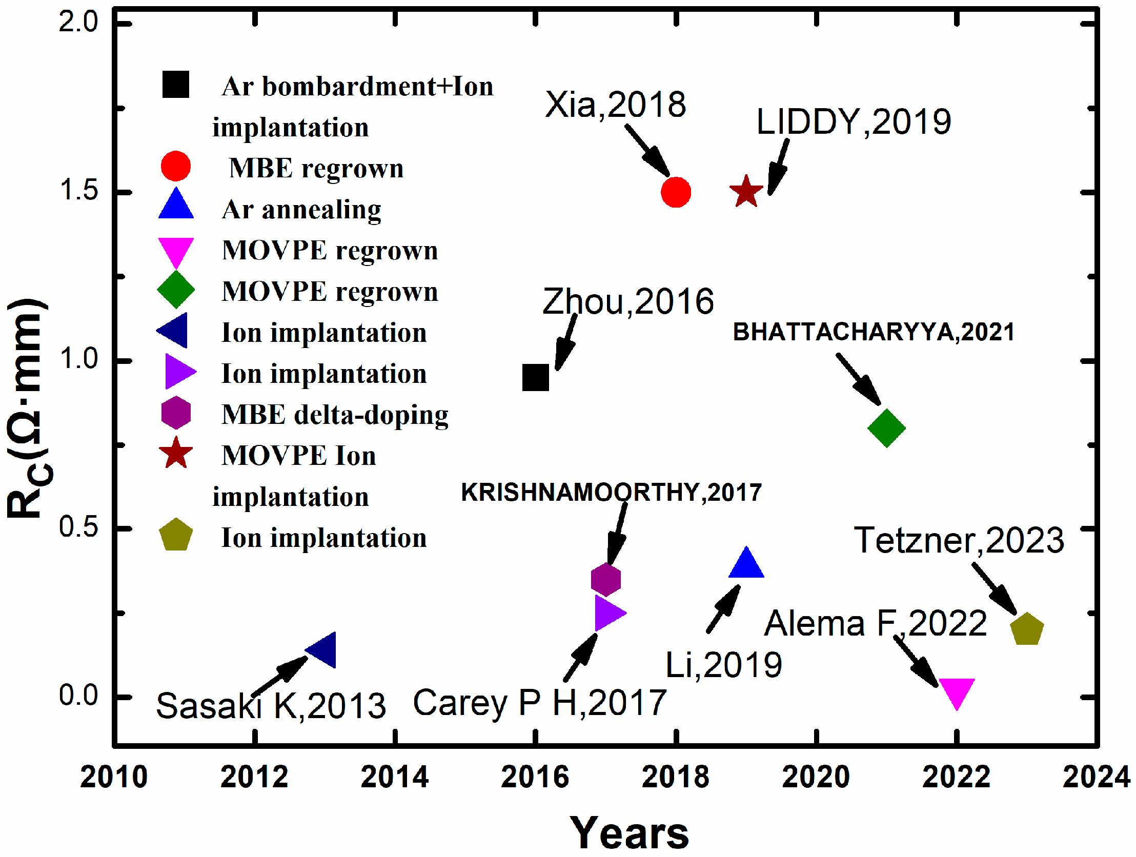
3.3. Ion Implantation

The ion-implantation doping technique (including Si, Sn, etc.) is another effective way for Ga2O3 to realize low-contact-resistance Ohmic electrodes by forming a heavily doped n+ region that facilitates electron flow. In 2013, Sasaki et al. [83] successfully fabricated Ohmic electrodes with a low contact resistance via Si implantation, which requires the MOVPE method in β-Ga2O3. They optimized the Si doping concentration to 5 × 1019 cm−3, which was activated by annealing at a temperature of 950 °C. The RC and ρc in their results were as low as 1.4 mΩ·cm and 4.6 × 10⁻⁶ Ω·cm−2, respectively. In other results, Zhou et al. [70] doped β-Ga2O3 with Sn at a concentration of 2.7 × 1018 cm−3. Combined with Ar plasma bombardment, the RC was dramatically reduced to 0.95 Ω·mm. The fabricated devices also exhibited an excellent on/off ratio and output characteristics and a low SS value. In addition, Ge and Sn were also studied for doping β-Ga2O3 [89]. In that study, the samples were treated under the same annealing condition (925 °C for 30 min). The efficiencies of Sn, Ge, and Si were calculated to be 28.2%, 40.3%, and 64.7%, respectively, using SIMS measurements. The same activation annealing condition for Ge and Sn with Si resulted in low activation efficiencies for Ge and Sn. The heavier Ge and Sn ions also created more implant damage than the Si ions due to the greater momentum transfer required to achieve the same implant depth, likely contributing to decreased implant activation and increasing both the contact and sheet resistances. In 2023, Tetzner et al. [90] analyzed the optimized annealing temperature for the activation of Ge-implanted β-Ga2O3 from 900 to 1200 °C using a pulsed RTA technique. The lowest recorded ρc value of 4.8 × 10⁻⁷ Ω cm−2 was achieved after a pulsed RTA at 1100 °C using 40 pulses. The activation efficiency was 14.2%. The measured RC and ρc values at various annealing temperatures can be seen in Figure 6. Also, other representative studies related to the ion implantation technique have been reported [91,92,93,94].
Considering the high cost of ion implantation, the complicated steps, and the potential damage-induced diffusion of species, Zeng et al. [95] successfully proposed a Sn spin-on-glass (SOG) technique for β-Ga2O3 doping. A Sn-doped epitaxial layer with a doping density of 1 × 1018 cm−3 was formed on a Ga2O3 substrate. The obtained ρc was determined to be 2.1 ± 1.4 × 10⁻⁵ Ω·cm−2 in their results. As shown in Figure 7, the fabricated devices also exhibited improved output current, peak transconductance, on/off ratio, and breakdown voltage values. The SOG technique is an effective alternative to the simple, low-cost doping technique to make low-RC Ohmic contact. Thus, based on the existing results using doping techniques, it is possible to form a heavily doped Ga2O3 layer and obtain ρc values from 10−5 to 10−7 Ω·cm−2.
Ion implantation, surface treatment, and post-RTA annealing are always used together to obtain a low RC. Ion implantation can form a heavily doped interface to enhance electron tunneling. A surface treatment combined with RTA can generate oxygen vacancies that act as donors in Ga2O3, resulting in a low RC. For ion implantation, a high-temperature post-anneal is required to activate the implanted donor impurity and recover the induced crystalline damage. During the high-temperature process, dopant redistribution, residuals, crystalline defects, and incomplete activation should be noticed and optimized.

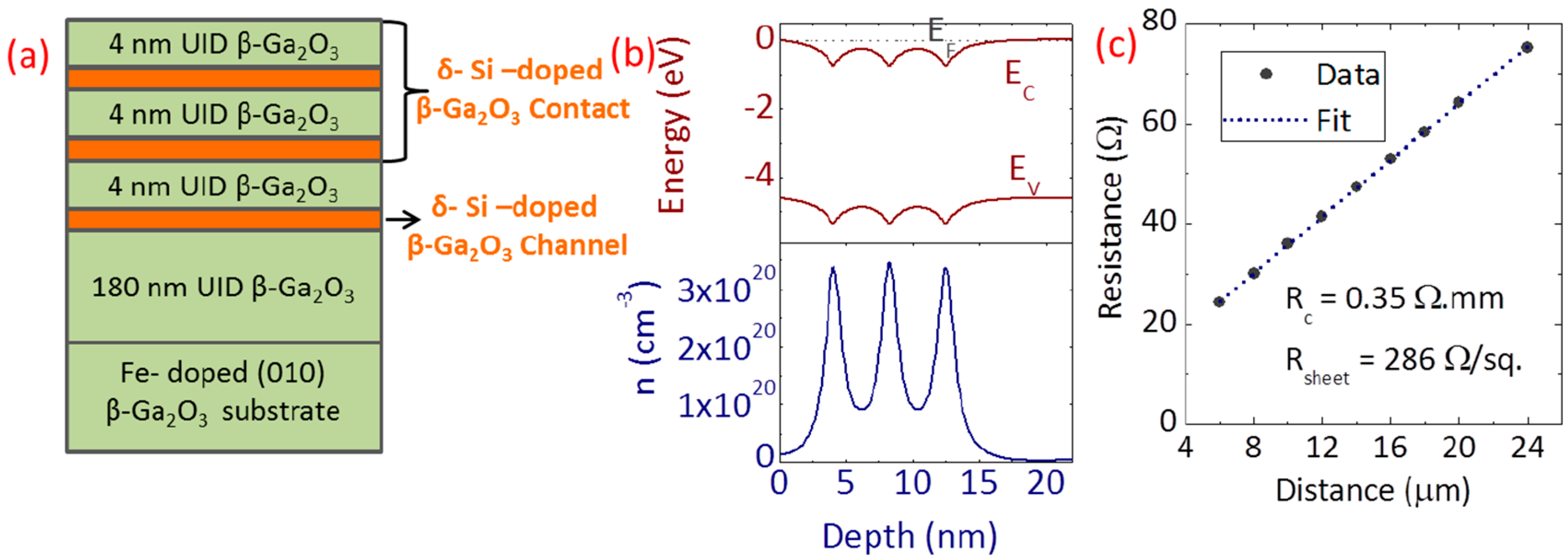
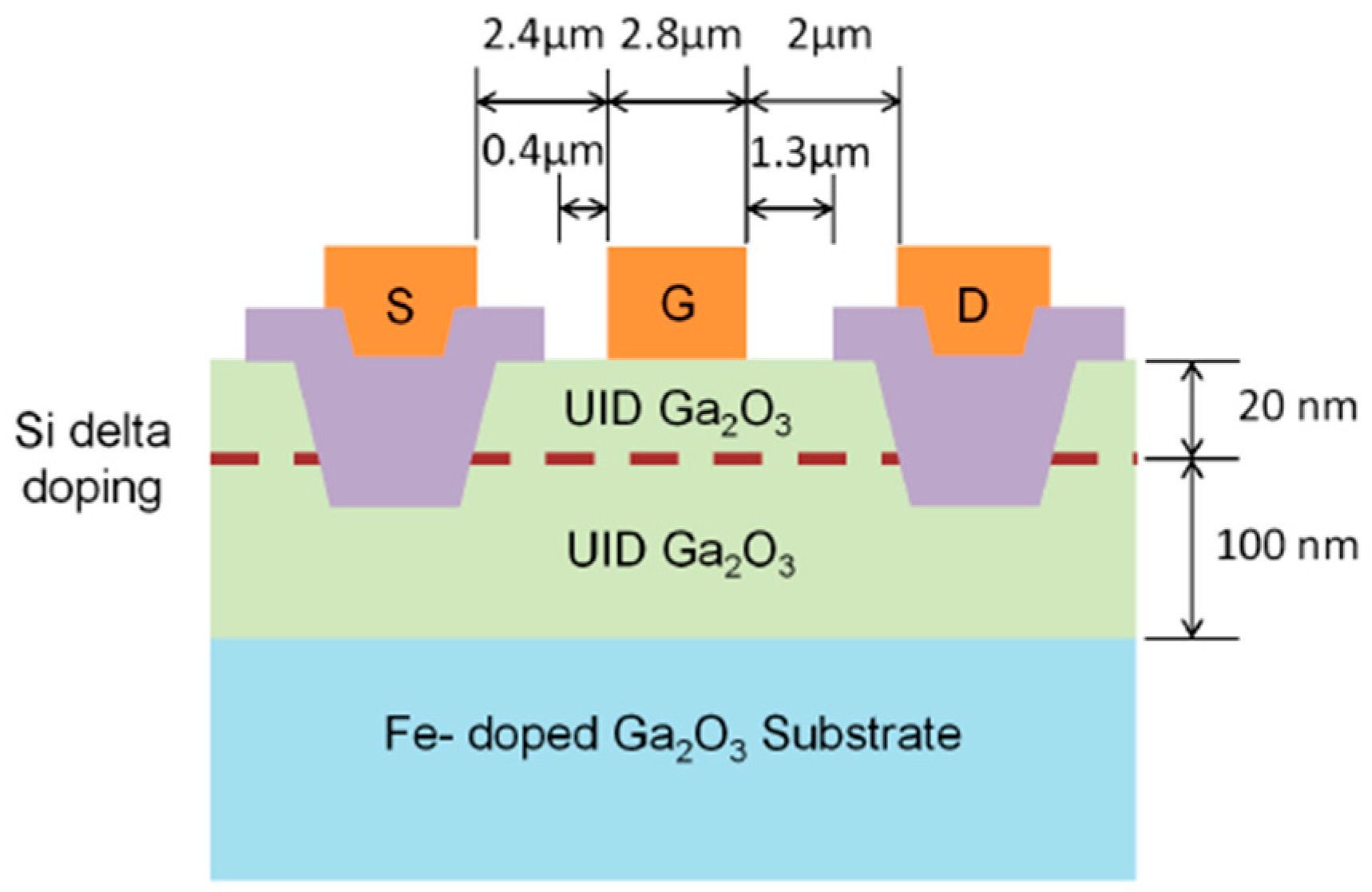
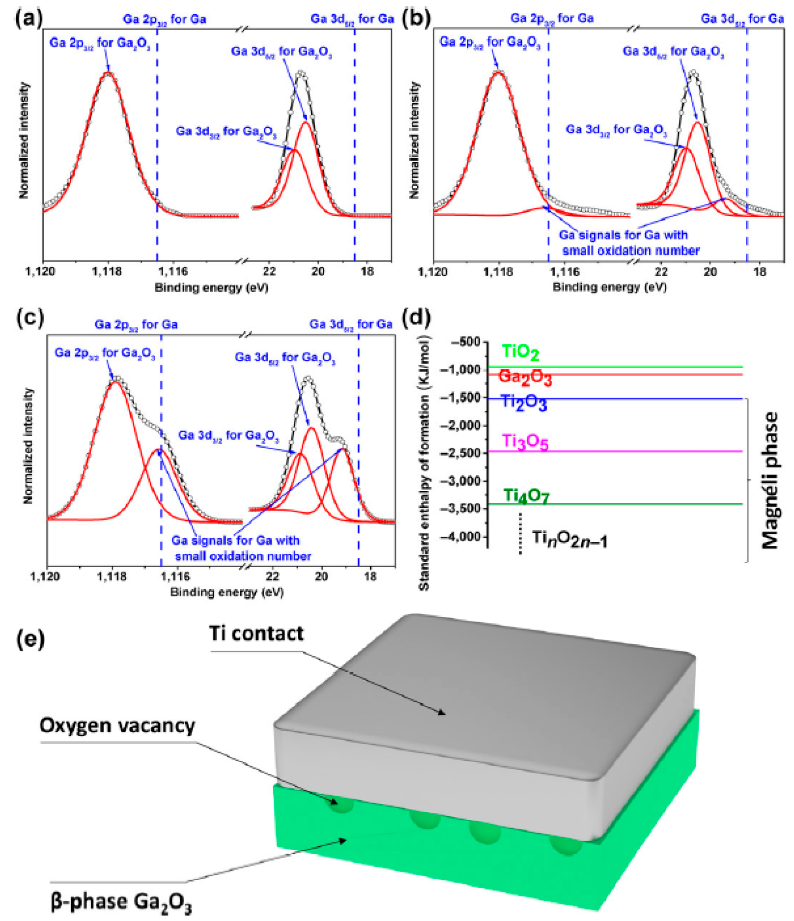
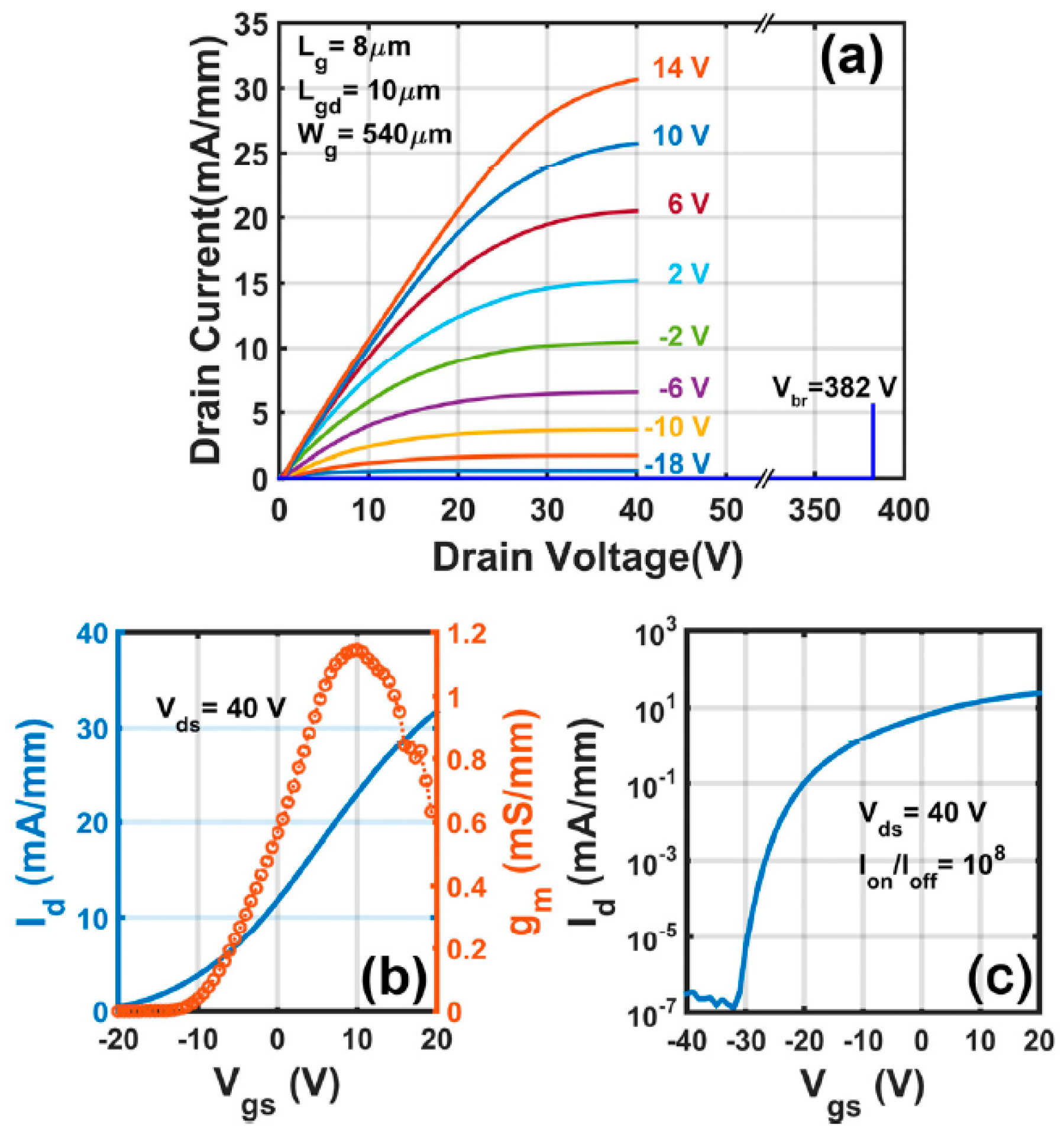
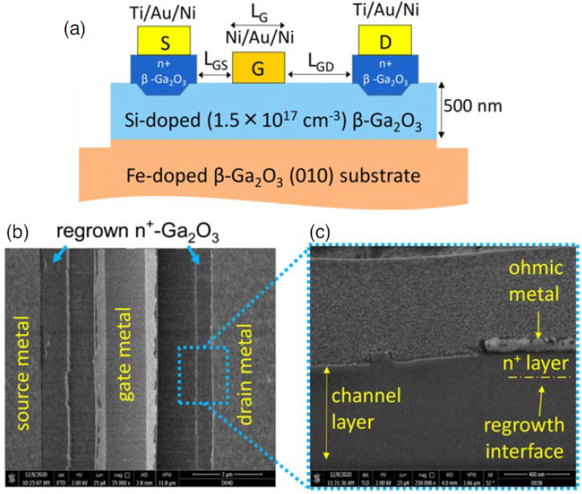
3.4. Epitaxial Regrowth

To further reduce the contact resistance, regrown contacts have been reported to fabricate Ohmic contacts. Ion implantation and spin-on-glass techniques need a high annealing temperature around 900–1200 °C and potentially deteriorate the material quality in the active region. However, the regrowth process, which is performed at a much lower temperature of about 600 °C can avoid this potential problem. In 2018, Xia et al. [32] used a molecular-beam epitaxy (MBE) method to form a heavily doped n-type Ga2O3 with a doping concentration of 2 × 1020 cm−3. The device’s structure can be seen in Figure 8. An extracted RC of 1.5 Ω·mm was obtained from the TLM structure. The regrowth technique avoids gate recessing and potential damage associated with etching, which may degrade the carrier mobility. The fabricated devices exhibited a peak drain current of 140 mA/mm and an excellent transconductance of 34 mS/mm. Considering the advantage of high room-temperature electron mobility values (close to the theoretical limit) grown using metalorganic vapor phase epitaxy (MOVPE), Bhattacharyya et al. [36] proposed an MOVPE epitaxy approach to realize low-resistance regrown S/D contacts in a Ga2O3 lateral MESFET for the first time. As shown in Figure 9, the heavily Si-doped (∼1.8 × 1020 cm−3) Ga2O3 was grown using MOVPE at a relatively low temperature of 600 °C. After that, an Ohmic metal stack of Ti/Au/Ni (20 nm/100 nm/30 nm) was evaporated, followed by 470 °C annealing in N2. From their testing results, an ultralow RC of 80 mΩ·mm and a ρc of 8.3 × 10⁻⁷ Ω·cm−2 were achieved. In order to systematically study the mechanism of heavily doped β-Ga2O3 using MOVPE to achieve low contact resistance, in 2022 Alema et al. [96] optimized the doping concentration to 3.23 × 1020 cm−3, and the RC and ρc values were as low as 1.62 × 10⁻⁷ Ω·cm−2 and 0.023 Ω·mm. The ultralow contact characteristics had a significant impact, improving the RF devices’ performance.
The existing results that have been reported in recent years demonstrate that regrown contact is an effective approach to achieve an ultralow RC. Epitaxial regrowth obtains a high-quality crystalline film and can be versatile. However, there are also several constraints, such as low throughput, high expense, strict material compatibility, and the need for selective growth or subsequent etchings, as mentioned in Refs. [97,98].

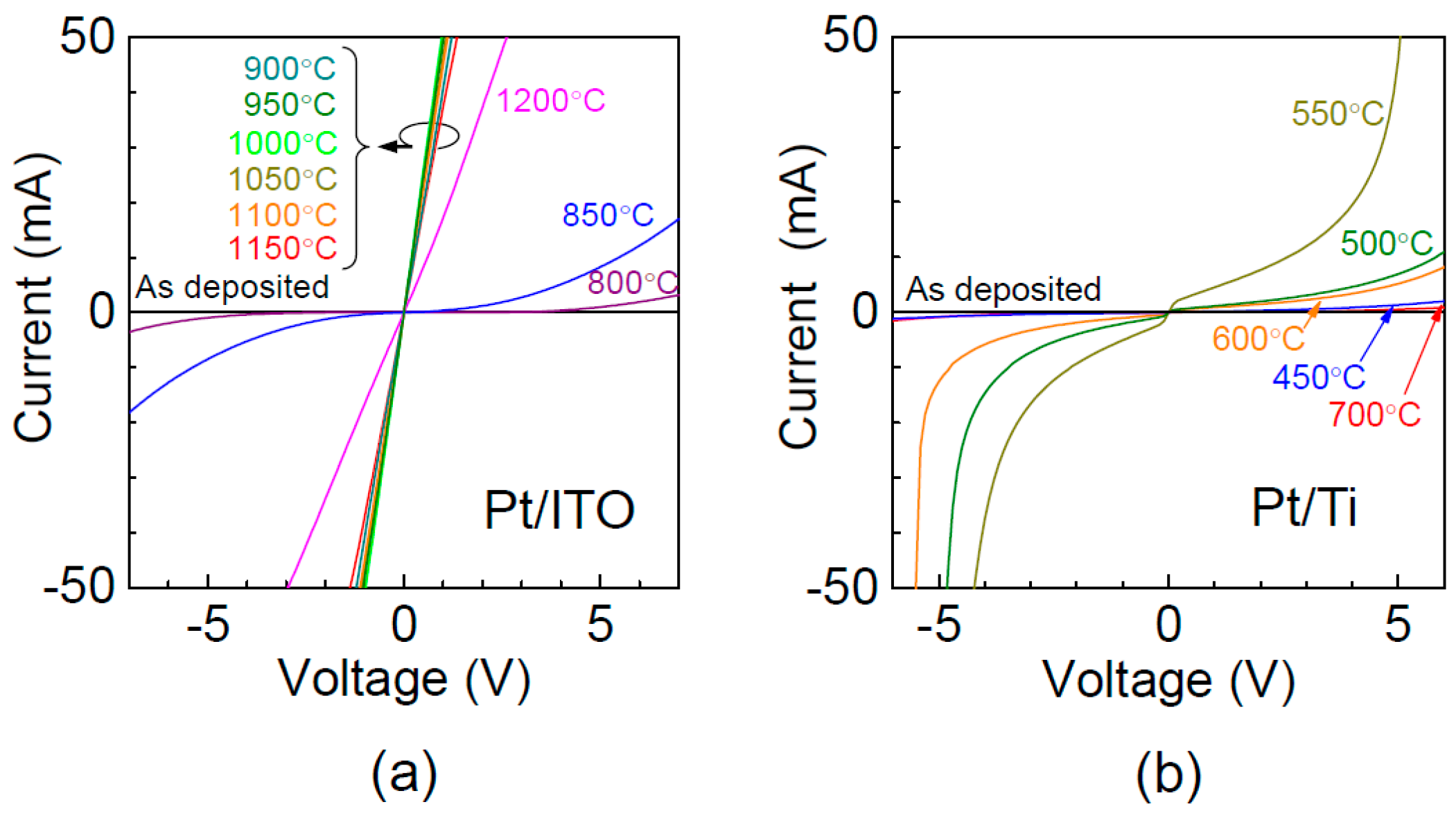
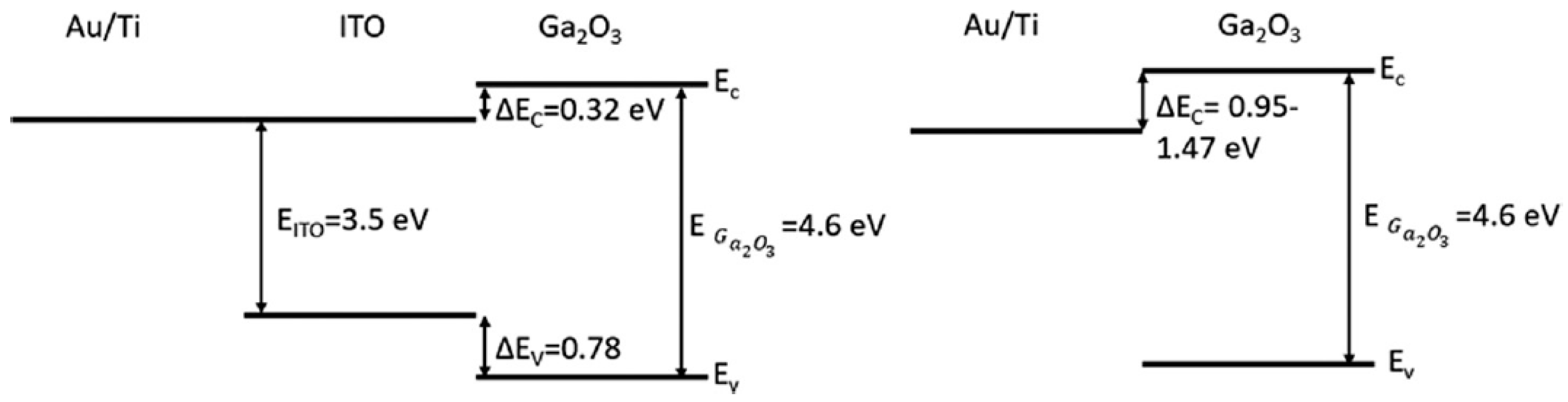
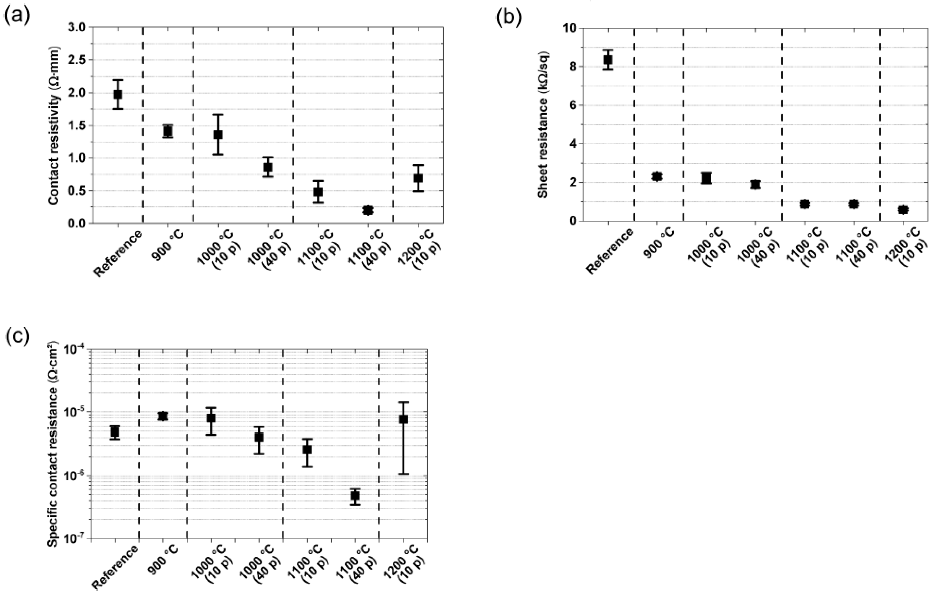
3.5. Adding the Interlayer

The Ti/Au schemes always form a 3–5 nm interlayer, which facilitates electron transport for Ohmic contact formation. Another approach is inserting an intermediate semiconductor layer (ISL) with a low work function and a narrower bandgap. In 2016, Oshima et al. [99] proved the insertion of indium tin oxide (ITO) for forming Ohmic contact with β-Ga2O3. In their results, as shown in Figure 10, the ITO method exhibited Ohmic behavior at temperatures from 900 °C to 1150 °C. However, Pt/β-Ga2O3 maintained Schottky contact, even at the RTA temperature of 500 °C. They also confirmed the existence of an intermediate semiconductor layer (ISL) at the interface using TEM and EDS analyses.
In 2017, considering the excellent conductivity property of ITO, by depositing an ITO layer before the metal deposition, Carey et al. created a Au/Ti/ITO/Si-doped Ga2O3 structure to form low-RC contact. As shown in Figure 11, by optimizing the annealing temperature at 600 °C, the minimum RC and ρc were determined to be 0.6 Ω·mm and 6.3 × 10⁻⁵ Ω·cm−2. A schematic of the band offset for Au/Ti/ITO on Ga2O3 and Au/Ti on Ga2O3 can be seen in Figure 12 [100]. The insertion of an ITO interlayer allows for reduced conduction band discontinuity between Ti and Ga2O3, which is beneficial for reducing RC values. By inserting an aluminum zinc oxide (AZO) interlayer [101], Au/Ti/AZO/Ga2O3 schemes exhibit the minimum RC and specific contact resistance values of 0.42 Ω·mm and 2.82 × 10⁻⁵ cm−2, respectively. The optimized annealing temperature is 400 °C, as shown in Figure 13. In their results, samples without an AZO interlayer did not exhibit Ohmic I–V characteristics when varying the annealing temperature. The use of a thin layer of AZO, with a bandgap of 3.2 eV, can lower the barrier for electron transport and achieve a low RC. A corresponding schematic of the band offset for AZO on Ga2O3 can be seen in Figure 14. Other related results have also been presented by other researchers [102,103,104,105]. It should be noted that different metal layers capping ITO layers are needed to prevent the degradation of the surface morphology.
Other elements such as substrate orientation have also been reported to influence the Ohmic contact property. To form Ohmic contact, Ti/Au contacts were deposited, followed by an RTA process at 450 °C for 5 min, which was employed on both ( 2 ¯ 01) and (010) Sn-doped Ga2O3. The former sample exhibited Ohmic characteristics compared to the rectifying behavior of the (010) sample. Related content has also been investigated and reported by other groups [106,107,108,109].
In recent years, researchers have investigated and optimized the Ohmic contact property of β-Ga2O3 by choosing a metal with a proper work function and investigating metal schemes, interfacial reactions between metal and semiconductors during the annealing process, and the doping concentration of Ga2O3 in the source/drain region, and they have achieved excellent results. Representative results with excellent Ohmic contact quality are summarized in Figure 15 [32,33,36,37,70,83,88,90,96,100]. Despite the significant improvement in the Ohmic contact techniques for β-Ga2O3, there are also some questions that need to be solved before commercializing the devices. (1) For power device applications, contact performance in high-temperature, -current, and -voltage environments is another concern. Failure analyses of the electrical stress/cycling of Ohmic electrodes have been investigated for other WBG semiconductor systems [110,111,112], while for β-Ga2O3, the research is lacking and efforts should be made to understand the degradation mechanism of Ohmic contacts under electrical stress. (2) To realize the integration of β-Ga2O3 semiconductors into Si CMOS technology, Au-free metal schemes should be investigated and proposed. The commonly used Ti/Au layer for Ga2O3 is not CMOS-compatible due to the existence of Au, which is a contaminant for Si fabrication lines [113,114]. Au is used for oxidation protection. Some oxidation-resistant capping materials, such as TiN, which has been proven to realize low-RC Ohmic contact in AlGaN/GaN HEMT [53], can be substitutes for Ohmic contact realization in β-Ga2O3 devices. Related investigations should be carried out to prove the feasibility of Au-free schemes. (3) RIE, ion implantation, and epitaxial regrowth are used to achieve a low RC. For the RIE process, the influences of plasma gas (including BCl3/Ar, Ar, and CF4 [115]), plasma power, bias power, etc., should be fully understood. For ion implantation, the high-temperature annealing used for impurity activation and damage recovery may cause unwanted effects, which should be noticed and further studied. In addition, the effect of substrate orientation should also be investigated. Other annealing techniques can also be used for Ohmic contact formation in β-Ga2O3 devices [116,117].

4. Conclusions

In this work, the β-Ga2O3 Ohmic contact technique has been discussed comprehensively, including the selected metal stack, surface treatment, ion implantation, epitaxial regrowth, adding the interlayer, etc. Although state-of-the-art methods for forming Ohmic contacts with β-Ga2O3 have been proposed and summarized in this work, there is still significant room for exploration to improve Ohmic contact, and related prospects have been proposed. In summary, Ohmic contacts with β-Ga2O3 will continue to be a research focus for power application in the future. We believe the content presented in this work will be beneficial for understanding and achieving high-performance β-Ga2O3 devices with low RC values.

Author Contributions

L.-Q.Z.: writing—original draft, investigation, data curation, and conceptualization; W.-Q.M., X.-L.W., J.-Y.D., S.-Y.Q., J.-J.L. and Y.-T.T.: writing—original draft, investigation, data curation, and conceptualization; Z.-Y.W., Q.X., Y.Z. and P.-F.W.: writing—review and editing, visualization, and validation. All authors have read and agreed to the published version of the manuscript.

Funding

This work was supported by the Henan Province Key Research and Development and Promotion of Special Scientific and Technological Research Project (Grant No. 222102320283), key scientific research projects of higher education institutions in Henan Province (Grant No. 22B510009), and in part by the Key Laboratory of Optoelectronic Sensing Integrated Application of Hennan Province.

Data Availability Statement

The authors declare that the data supporting the findings of this study are available within the article.

Conflicts of Interest

The authors declare no conflict of interest.

References

  1. Sonnenberg, T.; Verploegh, S.; Pinto, M.; Popović, Z. W-Band GaN HEMT Frequency Multipliers. IEEE Trans. Microw. Theory Tech. 2023, 71, 4327–4336. [Google Scholar] [CrossRef]
  2. Akso, E.; Collins, H.; Clymore, C.; Li, W.; Guidry, M.; Romanczyk, B.; Wurm, C.; Liu, W.; Hatui, N.; Hamwey, R.; et al. First Demonstration of Four-Finger N-polar GaN HEMT Exhibiting Record 712 mW Output Power With 31.7% PAE at 94 GHz. IEEE Microw. Wirel. Technol. Lett. 2023, 33, 683–686. [Google Scholar] [CrossRef]
  3. Han, L.; Tang, X.; Wang, Z.; Gong, W.; Zhai, R.; Jia, Z.; Zhang, W. Research Progress and Development Prospects of Enhanced GaN HEMTs. Crystals 2023, 13, 911. [Google Scholar] [CrossRef]
  4. Li, H.; Zhao, S.; Wang, X.; Ding, L.; Mantooth, A.H. Parallel Connection of Silicon Carbide MOSFETs Challenges, Mechanism, and Solutions. IEEE Trans. Power Electron. 2023, 38, 9731–9749. [Google Scholar] [CrossRef]
  5. Lyu, G.; Sun, J.; Wei, J.; Chen, K.J. Static and Dynamic Characteristics of a 1200 V/22 mΩ Normally-Off SiC/GaN Cascode Device Built with Parallel-Connected SiC JFETs Controlled by a Single GaN HEMT. IEEE Trans. Power Electron. 2023, 38, 12648–12658. [Google Scholar] [CrossRef]
  6. Roy, R.; Hill, V.G.; Osborn, E.F. Polymorphism of Ga2O3 and the system Ga2O3-H2O. J. Am. Chem. Soc. 1952, 74, 719–722. [Google Scholar] [CrossRef]
  7. Yoshioka, S.; Hayashi, H.; Kuwabara, A.; Oba, F.; Matsunaga, K.; Tanaka, I. Structures and energetics of Ga2O3 polymorphs. J. Phys. Condens. Matter 2007, 19, 346211. [Google Scholar] [CrossRef]
  8. Bechstedt, F.; Furthmüller, J. Influence of screening dynamics on excitons in Ga2O3 polymorphs. Appl. Phys. Lett. 2019, 114, 122101. [Google Scholar] [CrossRef]
  9. Pearton, S.J.; Yang, J.; Cary, P.H.; Ren, F.; Kim, J.; Tadjer, M.J.; Mastro, M.A. A review of Ga2O3 materials, processing, and devices. Appl. Phys. Rev. 2018, 5, 011301. [Google Scholar] [CrossRef]
  10. Wang, C.; Zhang, J.; Xu, S.; Zhang, C.; Feng, Q.; Zhang, Y.; Ning, J.; Zhao, S.; Zhou, H.; Hao, Y. Progress in state-of-the-art technologies of Ga2O3 devices. J. Phys. D Appl. Phys. 2021, 54, 243001. [Google Scholar] [CrossRef]
  11. Sheoran, H.; Kumar, V.; Singh, R. A comprehensive review on recent developments in ohmic and Schottky contacts on Ga2O3 for device applications. ACS Appl. Electron. Mater. 2022, 4, 2589–2628. [Google Scholar] [CrossRef]
  12. Abedi Rik, N.; Orouji, A.A.; Madadi, D. 500 V breakdown voltage in β-Ga2O3 laterally diffused metal-oxide-semiconductor field-effect transistor with 108 MW/cm2 power figure of merit. IET Circuits Devices Syst. 2023, 17, 199–204. [Google Scholar] [CrossRef]
  13. Wang, X.; Lu, X.; He, Y.; Liu, P.; Shao, Y.; Li, J.; Yang, Y.; Li, Y.; Hao, Y.; Ma, X. An E-mode β-Ga2O3 metal-heterojunction composite field effect transistor with a record high P-FOM of 0.73 GW/cm2. In Proceedings of the 2023 35th International Symposium on Power Semiconductor Devices and ICs (ISPSD), Hong Kong, 28 May–1 June 2023; pp. 390–393. [Google Scholar] [CrossRef]
  14. Liu, H.; Wang, Y.; Lv, Y.; Han, S.; Han, T.; Dun, S.; Guo, H.; Bu, A.; Feng, Z. 10-kV Lateral β-Ga2O3 MESFETs with B ion Implanted Planar Isolation. IEEE Electron. Device Lett. 2023, 44, 1048–1051. [Google Scholar] [CrossRef]
  15. Guo, W.; Han, Z.; Zhao, X.; Xu, G.; Long, S. Large-area β-Ga2O3 Schottky barrier diode and its application in DC-DC converters. J. Semicond. 2023, 44, 072805. [Google Scholar] [CrossRef]
  16. Wei, Y.; Peng, X.; Jiang, Z.; Sun, T.; Wei, J.; Yang, K.; Hao, L.; Luo, X. Low Reverse Conduction Loss β-Ga2O3 Vertical FinFET with an Integrated Fin Diode. IEEE Trans. Electron. Devices 2023, 70, 3454–3461. [Google Scholar] [CrossRef]
  17. Hao, W.; Wu, F.; Li, W.; Xu, G.; Xie, X.; Zhou, K.; Guo, W.; Zhou, X.; He, Q.; Zhao, X.; et al. Improved Vertical β-Ga2O3 Schottky Barrier Diodes with Conductivity-Modulated p-NiO Junction Termination Extension. IEEE Trans. Electron. Devices 2023, 70, 2129–2134. [Google Scholar] [CrossRef]
  18. Wu, F.; Wang, Y.; Jian, G.; Xu, G.; Zhou, X.; Guo, W.; Du, J.; Liu, Q.; Dun, S.; Yu, Z.; et al. Superior Performance β-Ga2O3 Junction Barrier Schottky Diodes Implementing p-NiO Heterojuntion and Beveled Field Plate for Hybrid Cockcroft–Walton Voltage Multiplier. IEEE Trans. Electron. Devices 2023, 70, 1199–1205. [Google Scholar] [CrossRef]
  19. Zhang, C.; Liu, K.; Ai, Q.; Sun, X.; Chen, X.; Yang, J.; Zhu, Y.; Cheng, Z.; Li, B.; Liu, L.; et al. High-performance fully transparent Ga2O3 solar-blind UV photodetector with the embedded indium-tin-oxide electrodes. Mater. Today Phys. 2023, 33, 101034. [Google Scholar] [CrossRef]
  20. Li, Y.; Deng, C.; Huang, B.; Yang, S.; Xu, J.; Zhang, G.; Hu, S.; Wang, D.; Liu, B.; Ji, Z.; et al. High-Performance Solar-Blind UV Phototransistors Based on ZnO/Ga2O3 Heterojunction Channels. ACS Appl. Mater. Interfaces 2023, 15, 18372–18378. [Google Scholar] [CrossRef]
  21. Zeng, G.; Zhang, M.R.; Chen, Y.C.; Li, X.; Chen, D.; Shi, C.; Zhao, X.; Chen, N.; Wang, T.; Zhang, W.; et al. A solar-blind photodetector with ultrahigh rectification ratio and photoresponsivity based on the MoTe2/Ta: β-Ga2O3 pn junction. Mater. Today Phys. 2023, 33, 101042. [Google Scholar] [CrossRef]
  22. Matys, M.; Kitagawa, K.; Narita, T.; Uesugi, T.; Suda, J.; Kachi, T. Mg-implanted vertical GaN junction barrier Schottky rectifiers with low on resistance, low turn-on voltage, and nearly ideal nondestructive breakdown voltage. Appl. Phys. Lett. 2022, 121, 203507. [Google Scholar] [CrossRef]
  23. Aida, H.; Nishiguchi, K.; Takeda, H.; Aota, N.; Sunakawa, K.; Yaguchi, Y. Growth of β-Ga2O3 single crystals by the edge-defined, film fed growth method. Jpn. J. Appl. Phys. 2008, 47, 8506. [Google Scholar] [CrossRef]
  24. Ohira, S.; Suzuki, N.; Arai, N.; Tanaka, M.; Sugawara, T.; Nakajima, K.; Shishido, T. Characterization of transparent and conducting Sn-doped β-Ga2O3 single crystal after annealing. Thin Solid Film. 2008, 516, 5763–5767. [Google Scholar] [CrossRef]
  25. Víllora, E.G.; Shimamura, K.; Yoshikawa, Y.; Aoki, K.; Ichinose, N. Large-size β-Ga2O3 single crystals and wafers. J. Cryst. Growth 2004, 270, 420–426. [Google Scholar] [CrossRef]
  26. Hoshikawa, K.; Ohba, E.; Kobayashi, T.; Yanagisawa, J.; Miyagawa, C.; Nakamura, Y. Growth of β-Ga2O3 single crystals using vertical Bridgman method in ambient air. J. Cryst. Growth 2016, 447, 36–41. [Google Scholar] [CrossRef]
  27. Nikolaev, V.I.; Maslov, V.; Stepanov, S.I.; Pechnikov, A.I.; Krymov, V.; Nikitina, I.P.; Guzilova, L.I.; Bougrov, V.E.; Romanov, A.E. Growth and characterization of β-Ga2O3 crystals. J. Cryst. Growth 2017, 457, 132–136. [Google Scholar] [CrossRef]
  28. Tomm, Y.; Reiche, P.; Klimm, D.; Fukuda, T. Czochralski grown Ga2O3 crystals. J. Cryst. Growth 2000, 220, 510–514. [Google Scholar] [CrossRef]
  29. Galazka, Z.; Uecker, R.; Irmscher, K.; Albrecht, M.; Klimm, D.; Pietsch, M.; Brützam, M.; Bertram, R.; Ganschow, S.; Fornari, R. Czochralski growth and characterization of β-Ga2O3 single crystals. Cryst. Res. Technol. 2010, 45, 1229–1236. [Google Scholar] [CrossRef]
  30. Alema, F.; Seryogin, G.; Osinsky, A.; Osinsky, A. Ge doping of β-Ga2O3 by MOCVD. APL Mater. 2021, 9, 091102. [Google Scholar] [CrossRef]
  31. Seryogin, G.; Alema, F.; Valente, N.; Fu, H.; Steinbrunner, E.; Neal, A.; Mou, S.; Fine, A.; Osinsky, A. MOCVD growth of high purity Ga2O3 epitaxial films using trimethylgallium precursor. Appl. Phys. Lett. 2020, 117, 262101. [Google Scholar] [CrossRef]
  32. Xia, Z.; Joishi, C.; Krishnamoorthy, S.; Bajaj, S.; Zhang, Y.; Brenner, M.; Lodha, S.; Rajan, S. Delta Doped β-Ga2O3 Field Effect Transistors with Regrown Ohmic Contacts. IEEE Electron. Device Lett. 2018, 39, 568–571. [Google Scholar] [CrossRef]
  33. Krishnamoorthy, S.; Xia, Z.; Bajaj, S.; Brenner, M.; Rajan, S. Delta-doped β-gallium oxide field-effect transistor. Appl. Phys. Express 2017, 10, 051102. [Google Scholar] [CrossRef]
  34. Oshima, Y.; Víllora, E.G.; Shimamura, K. Halide vapor phase epitaxy of twin-free α-Ga2O3 on sapphire (0001) substrates. Appl. Phys. Express 2015, 8, 055501. [Google Scholar] [CrossRef]
  35. Murakami, H.; Nomura, K.; Goto, K.; Sasaki, K.; Kawara, K.; Thieu, Q.; Togashi, R.; Kumagai, Y.; Higashiwaki, M.; Kuramata, A.; et al. Homoepitaxial growth of β-Ga2O3 layers by halide vapor phase epitaxy. Appl. Phys. Express 2014, 8, 015503. [Google Scholar] [CrossRef]
  36. Bhattacharyya, A.; Roy, S.; Ranga, P.; Shoemaker, D.; Song, Y.; Lundh, J.; Choi, S.; Krishnamoorthy, S. 130 mA mm−1 β-Ga2O3 metal semiconductor field effect transistor with low-temperature metalorganic vapor phase epitaxy-regrown ohmic contacts. Appl. Phys. Express 2021, 14, 076502. [Google Scholar] [CrossRef]
  37. Liddy, K.J.; Green, A.; Hendricks, N.; Heller, E.; Moser, N.; Leedy, K.; Popp, A.; Lindquist, M.; Tetlak, S.; Wagner, G.; et al. Thin channel β-Ga2O3 MOSFETs with self-aligned refractory metal gates. Appl. Phys. Express 2019, 12, 126501. [Google Scholar] [CrossRef]
  38. Varley, J.B.; Janotti, A.; Franchini, C.; Walle, C. Role of self-trap in luminescence and p-type conductivity of wide-band-gap oxides. Phys. Rev. B 2012, 85, 081109. [Google Scholar] [CrossRef]
  39. Lyons, J.L. A survey of acceptor dopants for β-Ga2O3. Semicond. Sci. Technol. 2018, 33, 05LT02. [Google Scholar] [CrossRef]
  40. Gallagher, J.C.; Koehler, A.D.; Tadjer, M.J.; Mahadik, A.; Anderson, T.; Budhathoki, S.; Law, K.; Hauser, A.; Hobart, K.; Kub, F. Demonstration of Cul as a P-N heterojunction to β-Ga2O3. Appl. Phys. Express 2019, 12, 104005. [Google Scholar] [CrossRef]
  41. Budde, M.; Splith, D.; Mazzolini, P.; Tahraoui, A.; Feld, J.; Ramsteiner, M.; Wenckstern, H.; Grundmann, M.; Bierwage, O. SnO/β-Ga2O3 vertical pn heterojunction diodes. Appl. Phys. Lett. 2020, 117, 252106. [Google Scholar] [CrossRef]
  42. Watahiki, T.; Yuda, Y.; Furukawa, A.; Yamamuka, M.; Takiguchi, Y.; Miyajima, S. Heterojunction p-Cu2O/n-Ga2O3 diode with high breakdown voltage. Appl. Phys. Lett. 2017, 111, 222104. [Google Scholar] [CrossRef]
  43. Lu, X.; Zhou, X.; Jiang, H.; Ng, K.; Chen, Z.; Pei, Y.; Lau, K.; Wang, G. 1-kV Sputtered p-NiO/n-Ga2O3 Heterojunction Diodes With an Ultra-Low Leakage Current Below 1μA/cm2. IEEE Electron. Device Lett. 2020, 41, 449–452. [Google Scholar] [CrossRef]
  44. Wang, Y.G.; Gong, H.H.; Lv, Y.J.; Fu, X.; Dun, S.; Han, T.; Liu, H.; Zhou, X.; Liang, S.; Zhang, R.; et al. 2.41 kV vertical P-NiO/n-Ga2O3 heterojunction diodes with a record Baliga’s figure-of-merit of 5.18 GW/cm2. IEEE Trans Power Electron. 2022, 37, 3743. [Google Scholar] [CrossRef]
  45. Nakagomi, S.; Hiratsuka, K.; Kakuda, Y.; Yoshihiro, K. Beta-gallium oxide/SiC heterojunction diodes with high rectification ratios. ECS J. Solid State Sci. Technol. 2016, 6, Q3030. [Google Scholar] [CrossRef]
  46. Zhang, Y.C.; Li, Y.F.; Wang, Z.Z.; Guo, R.; Xu, S.; Liu, C.; Zhao, S.; Zhang, J.; Hao, Y. Investigation of β-Ga2O3 films and β-Ga2O3/GaN heterostructures grown by metal organic chemical vapor deposition. Sci. China Phys. Mech. Astron. 2020, 63, 117311. [Google Scholar] [CrossRef]
  47. Jaquez, M.; Specht, P.; Yu, K.M.; Walukiewicz, W.; Dubon, D. Amorphous gallium oxide sulfide: A highly mismatched alloy. J. Appl. Phys. 2019, 126, 105708. [Google Scholar] [CrossRef]
  48. Cai, X.; Sabino, F.P.; Janotti, A.; Wei, S. Approach to achieving a p-type transparent conducting oxide: Doping of bismuth-alloyed Ga2O3 with a strongly correlated band edge state. Phys. Rev. B 2021, 103, 115205. [Google Scholar] [CrossRef]
  49. Kaneko, K.; Masuda, Y.; Kan, S.; Takahashi, I.; Kato, Y.; Shinohe, T.; Fujita, S. Ultra-wide bandgap corundum-structured p-type α-(Ir, Ga) 2O3 alloys for α-Ga2O3 electronics. Appl. Phys. Lett. 2021, 118, 102104. [Google Scholar] [CrossRef]
  50. Li, Z.H.; Egbo, K.O.; Lv, X.H.; Wang, Y.; Yu, K. Electronic structure and properties of Cu2-xS thin films: Dependence of phase structures and free-hole concentrations. Appl. Surf. Sci. 2022, 572, 151530. [Google Scholar] [CrossRef]
  51. Ezeh, C.V.; Egbo, K.O.; Musah, J.D.; Yu, K.M. Wide gap p-type NiO-Ga2O3 alloy via electronic band engineering. J. Alloys Compd. 2023, 932, 167275. [Google Scholar] [CrossRef]
  52. Fan, M.Y.; Yang, G.Y.; Zhou, G.N.; Jiang, Y.; Li, W.; Jiang, Y.; Yu, H. Ultra-low Contact Resistivity of< 0.1 Ω mm for Au-free TixAly Alloy Contact on Non-recessed i-AlGaN/GaN. IEEE Electron. Device Lett. 2020, 41, 143–146. [Google Scholar] [CrossRef]
  53. Zhang, J.; Kang, X.; Wang, X.; Huang, S.; Chen, C.; Kei, K.; Zheng, Y.; Zhou, Q.; Chen, W.; Zhang, B.; et al. Ultralow-Contact-Resistance Au-Free Ohmic Contacts With Low Annealing Temperature on AlGaN/GaN Heterostructures. IEEE Electron. Device Lett. 2018, 39, 847–850. [Google Scholar] [CrossRef]
  54. Xu, R.; Lin, N.; Jia, Z.; Liu, Y.; Wang, H.; Yu, Y.; Zhao, X. First principles study of Schottky barriers at Ga2O3(100)/metal interfaces. RSC Adv. 2020, 10, 14746–14752. [Google Scholar] [CrossRef] [PubMed]
  55. Lovejoy, T.C.; Chen, R.; Zheng, X.; Villora, E.; Shimamura, K.; Yoshikawa, H.; Yamashita, Y.; Ueda, S.; Kobayashi, K.; Dunham, S.; et al. Band bending and surface defects in β-Ga2O3. Appl. Phys. Lett. 2012, 100, 181602. [Google Scholar] [CrossRef]
  56. Yao, Y.; Gangireddy, R.; Kim, J.; Das, K.; Davis, R.; Porter, L. Electrical behavior of β-Ga2O3 Schottky diodes with different Schottky metals. J. Vac. Sci. Technol. B 2017, 35, 03D113. [Google Scholar] [CrossRef]
  57. Mott, N.F. Note on the contact between a metal and an insulator or semi-conductor. In Mathematical Proceedings of the Cambridge Philosophical Society; Cambridge University Press: Cambridge, UK, 1938; pp. 568–572. [Google Scholar]
  58. Sze, S.M.; Ng, K.K. Physics of Semiconductor Devices; John Wiley & Sons: Hoboken, NJ, USA, 2006. [Google Scholar]
  59. Neamen, D. Semiconductor Physics and Devices; McGraw-Hill, Inc.: New York, NY, USA, 2002. [Google Scholar]
  60. Mohamed, M.; Irmscher, K.; Janowitz, C.; Galazka, Z.; Manzke, R.; Fornari, R. Schottky barrier height of Au on the transparent semiconducting oxide β-Ga2O3. Appl. Phys. Lett. 2012, 101, 132106. [Google Scholar] [CrossRef]
  61. Sze, S.M. Physics of Semiconductor Devices, 2nd ed.; Wily: New York, NY, USA, 1982. [Google Scholar]
  62. Rideout, V.L. A review of the theory and technology for ohmic contacts to group III-V compound semiconductors. Solid-State Electron. 1975, 18, 541–550. [Google Scholar] [CrossRef]
  63. Reeves, G.K.; Harrison, H.B. Obtaining the specific contact resistance from transmission line model measurements. IEEE Electron. Device Lett. 1982, 3, 111–113. [Google Scholar] [CrossRef]
  64. Schroder, D.K. Contact Resistance and Schottky Barriers; Wiley: New York, NY, USA, 2006. [Google Scholar]
  65. Yao, Y.; Davis, R.F.; Porter, L.M. Investigation of different metals as ohmic contacts to β-Ga2O3: Comparison and analysis of electrical behavior, morphology, and other physical properties. J. Electron. Mater. 2017, 46, 2053–2060. [Google Scholar] [CrossRef]
  66. Shi, J.; Xia, X.; Liang, H.; Abbas, Q.; Liu, J.; Zhang, H.; Liu, Y. Low resistivity ohmic contacts on lightly doped n-type β-Ga2O3 using Mg/Au. J. Mater. Sci. Mater. Electron. 2019, 30, 3860–3864. [Google Scholar] [CrossRef]
  67. Ma, J.; Yoo, G. Low Subthreshold Swing Double-Gate β-Ga2O3 Field-Effect Transistors with Polycrystalline Hafnium Oxide Dielectrics. IEEE Electron. Device Lett. 2019, 40, 1317–1320. [Google Scholar] [CrossRef]
  68. Lee, M.-H.; Peterson, R.L. Interfacial reactions of titanium/gold ohmic contacts with Sn-doped β-Ga2O3. APL Mater. 2019, 7, 022524. [Google Scholar] [CrossRef]
  69. Higashiwaki, M.; Sasaki, K.; Kamimura, T.; Wong, M.; Krishnamurthy, D.; Kuramata, A.; Masui, T.; Yamakoshi, S. Depletion-mode Ga2O3 metal-oxide-semiconductor field-effect transistors on β-Ga2O3 (010) substrates and temperature dependence of their device characteristics. Appl. Phys. Lett. 2013, 103, 123511. [Google Scholar] [CrossRef]
  70. Zhou, H.; Si, M.; Alghamdi, S.; Qiu, G.; Yang, L.; Ye, P. High-Performance Depletion/Enhancement-mode β-Ga2O3 on Insulator (GOOI) Field-Effect Transistors with Record Drain Currents of 600/450 mA/mm. IEEE Electron. Device Lett. 2016, 38, 103–106. [Google Scholar] [CrossRef]
  71. Zhou, H.; Maize, K.; Qiu, G.; Shakouri, A.; Ye, P. β-Ga2O3 on insulator field-effect transistors with drain currents exceeding 1.5 A/mm and their self-heating effect. Appl. Phys. Lett. 2017, 111, 092102. [Google Scholar] [CrossRef]
  72. Chabak, K.D.; Moser, N.; Green, A.; Jr, D.; Tetlak, S.; Heller, E.; Crespo, A.; Fitch, R.; McCandless, J.; Leedy, K.; et al. Enhancement-mode Ga2O3 wrap-gate fin field-effect transistors on native (100) β-Ga2O3 substrate with high breakdown voltage. Appl. Phys. Lett. 2016, 109, 213501. [Google Scholar] [CrossRef]
  73. Chen, J.; Li, X.; Ma, H.; Huang, W.; Ji, Z.; Xia, C.; Lu, H.; Zhang, W. Investigation of the mechanism for Ohmic contact formation in Ti/Al/Ni/Au contacts to β-Ga2O3 nanobelt field-effect transistors. ACS Appl. Mater. Interfaces 2019, 11, 32127–32134. [Google Scholar] [CrossRef]
  74. Gong, R.; Wang, J.; Liu, S.; Dong, Z.; Yu, M.; Wen, C.; Cai, Y.; Zhang, B. Analysis of surface roughness in Ti/Al/Ni/Au ohmic contact to AlGaN/GaN high electron mobility transistors. Appl. Phys. Lett. 2010, 97, 062115. [Google Scholar] [CrossRef]
  75. Fontserè, A.; Tomás, A.; Placidi, M.; Llobet, J.; Baron, N.; Chenot, S.; Cordier, Y.; Moreno, J.; Gammon, P.; Jennings, M.; et al. Micro and nano analysis of 0.2 Ω mm Ti/Al/Ni/Au ohmic contact to AlGaN/GaN. Appl. Phys. Lett. 2011, 99, 213504. [Google Scholar] [CrossRef]
  76. Tetzner, K.; Schewski, R.; Popp, A.; Anooz, S.; Chou, T.; Ostermay, I.; Kirmse, H.; Würfl, J. Refractory metal-based ohmic contacts on β-Ga2O3 using TiW. APL Mater. 2022, 10, 071108. [Google Scholar] [CrossRef]
  77. Lee, M.H.; Chou, T.S.; Bin Anooz, S.; Galazka, Z.; Popp, A.; Peterson, R. Effect of post-metallization anneal on (100) Ga2O3/Ti-Au ohmic contact performance and interfacial degradation. APL Mater. 2022, 10, 091105. [Google Scholar] [CrossRef]
  78. Kim, Y.; Kim, M.K.; Baik, K.H.; Jang, S. Low-resistance Ti/Au ohmic contact on (001) plane Ga2O3 Crystal. ECS J. Solid State Sci. Technol. 2022, 11, 045003. [Google Scholar] [CrossRef]
  79. Porter, L.M.; Hajzus, J.R. Perspectives from research on metal-semiconductor contacts: Examples from Ga2O3, SiC, (nano) diamond, and SnS. J. Vac. Sci. Technol. A 2020, 38, 031005. [Google Scholar] [CrossRef]
  80. Lyle, L.A.M.; Back, T.C.; Bowers, C.T.; Green, A.; Chabak, K.; Dorsey, D.; Heller, E.; Porter, L.M. Electrical and chemical analysis of Ti/Au contacts to β-Ga2O3. APL Mater. 2021, 9, 061104. [Google Scholar] [CrossRef]
  81. Guo, D.Y.; Wu, Z.P.; An, Y.H.; Guo, X.C.; Chu, X.L.; Sun, C.L.; Li, L.H.; Li, P.G.; Tang, W.H. Oxygen vacancy tuned Ohmic-Schottky conversion for enhanced performance in β-Ga2O3 solar-blind ultraviolet photodetectors. Appl. Phys. Lett. 2014, 105, 023507. [Google Scholar] [CrossRef]
  82. Higashiwaki, M.; Sasaki, K.; Kuramata, A.; Masui, T.; Yamakoshi, S. Gallium oxide (Ga2O3) metal-semiconductor field-effect transistors on single-crystal β-Ga2O3 (010) substrates. Appl. Phys. Lett. 2012, 100, 013504. [Google Scholar] [CrossRef]
  83. Sasaki, K.; Higashiwaki, M.; Kuramata, A.; Masui, T.; Yamakoshi, S. Si-ion implantation doping in β-Ga2O3 and its application to fabrication of low-resistance ohmic contacts. Appl. Phys. Express 2013, 6, 086502. [Google Scholar] [CrossRef]
  84. Oshima, T.; Okuno, T.; Arai, N.; Suzuki, N.; Ohira, S.; Fujita, S. Vertical solar-blind deep-ultraviolet Schottky photodetectors based on β-Ga2O3 substrates. Appl. Phys. Express 2008, 1, 011202. [Google Scholar] [CrossRef]
  85. Wong, M.H.; Sasaki, K.; Kuramata, A.; Yamakoshi, S.; Higashiwaki, M. Field-plated Ga2O3 MOSFETs with a breakdown voltage of over 750 V. IEEE Electron. Device Lett. 2015, 37, 212–215. [Google Scholar] [CrossRef]
  86. Higashiwaki, M.; Kuramata, A.; Murakami, H.; Kumagai, Y. State-of-the-art technologies of gallium oxide power devices. J. Phys. D Appl. Phys. 2017, 50, 333002. [Google Scholar] [CrossRef]
  87. Bae, J.; Kim, H.Y.; Kim, J. Contacting mechanically exfoliated β-Ga2O3 nanobelts for (opto) electronic device applications. ECS J. Solid State Sci. Technol. 2016, 6, Q3045. [Google Scholar] [CrossRef]
  88. Li, Z.; Liu, Y.; Zhang, A.; Liu, Q.; Shen, C.; Wu, F.; Xu, C.; Chen, M.; Fu, H.; Zhou, C. Quasi-two-dimensional β-Ga2O3 field effect transistors with large drain current density and low contact resistance via controlled formation of interfacial oxygen vacancies. Nano Res. 2019, 12, 143–148. [Google Scholar] [CrossRef]
  89. Spencer, J.A.; Tadjer, M.J.; Jacobs, A.G.; Mastro, M.A.; Lyons, J.L.; Freitas, J.A., Jr.; Gallagher, J.C.; Thieu, Q.T.; Sasaki, K.; Kuramata, A.; et al. Activation of implanted Si, Ge, and Sn donors in high-resistivity halide vapor phase epitaxial β-Ga2O3: N with high mobility. Appl. Phys. Lett 2022, 121, 192102. [Google Scholar] [CrossRef]
  90. Tetzner, K.; Thies, A.; Seyidov, P.; Chou, T.; Rehm, J.; Ostermay, J.; Galazka, Z.; Fiedler, A.; Popp, A.; Würfl, J. Ge-ion implantation and activation in (100) β-Ga2O3 for ohmic contact improvement using pulsed rapid thermal annealing. J. Vac. Sci. Technol. A 2023, 41, 043102. [Google Scholar] [CrossRef]
  91. Tadjer, M.; Lyons, J.; Nepal, N.; Freitas, J.A., Jr.; Koehler, A.; Foster, G. Review-Theory and characterization of doping and defects in β-Ga2O3. ECS J. Solid State Sci. Technol. 2019, 8, Q3187–Q3194. [Google Scholar] [CrossRef]
  92. Nikolskaya, A.; Okulich, E.; Korolev, D.; Stepanov, A.; Nikolichev, D.; Mikhaylov, A.; Tetelbaum, D.; Almaev, A.; Bolzan, C.A.; Buaczik, A., Jr.; et al. Ion implantation in β-Ga2O3: Physics and technology. J. Vac. Sci. Technol. A 2021, 39, 030802. [Google Scholar] [CrossRef]
  93. Huang, H.L.; Chae, C.; Johnson, J.M.; Senckowski, A.; Sharma, S.; Singisetti, U.; Wong, M.; Hwang, J. Atomic scale defect formation and phase transformation in Si implanted β-Ga2O3. APL Mater. 2023, 11, 061113. [Google Scholar] [CrossRef]
  94. Lee, M.H.; Chou, T.S.; Bin Anooz, S.; Galazka, Z.; Popp, A.; Peterson, R. Exploiting the nanostructural anisotropy of β-Ga2O3 to demonstrate giant improvement in titanium/gold ohmic contacts. ACS Nano 2022, 16, 11988–11997. [Google Scholar] [CrossRef]
  95. Zeng, K.; Wallace, J.S.; Heimburger, C.; Sasaki, K.; Kuramata, A.; Masui, T.; Gardella, J.; Singisetti, U. Ga2O3 MOSFETs using spin-on-glass source/drain doping technology. IEEE Electron. Device Lett. 2017, 38, 513–516. [Google Scholar] [CrossRef]
  96. Alema, F.; Peterson, C.; Bhattacharyya, A.; Roy, S.; Krishnamoorthy, S.; Osinsky, A. Low resistance Ohmic contact on epitaxial MOVPE grown β-Ga2O3 and β-(AlxGa1-x)2O3 films. IEEE Electron. Device Lett. 2022, 43, 1649–1652. [Google Scholar] [CrossRef]
  97. Lee, M.H.; Peterson, R.L. Process and characterization of ohmic contacts for beta-phase gallium oxide. J. Mater. Res. 2021, 36, 4771–4789. [Google Scholar] [CrossRef]
  98. Kim, H. Control and understanding of metal contacts to β-Ga2O3 single crystals: A review. SN Appl. Sci. 2022, 4, 27. [Google Scholar] [CrossRef]
  99. Oshima, T.; Wakabayashi, R.; Hattori, M.; Hashiguchi, A.; Kawano, N.; Sasaki, K.; Masui, T.; Kuramata, A.; Yamakoshi, S.; Yoshimatsu, K. Formation of indium-tin oxide ohmic contacts for β-Ga2O3. Jpn. J. Appl. Phys. 2016, 55, 1202B7. [Google Scholar] [CrossRef]
  100. Carey, P.H.; Yang, J.; Ren, F.; Hays, D.; Pearton, S.; Kuramata, A.; Kravchenko, I. Improvement of Ohmic contacts on Ga2O3 through use of ITO-interlayers. J. Vac. Sci. Technol. B 2017, 35, 061201. [Google Scholar] [CrossRef]
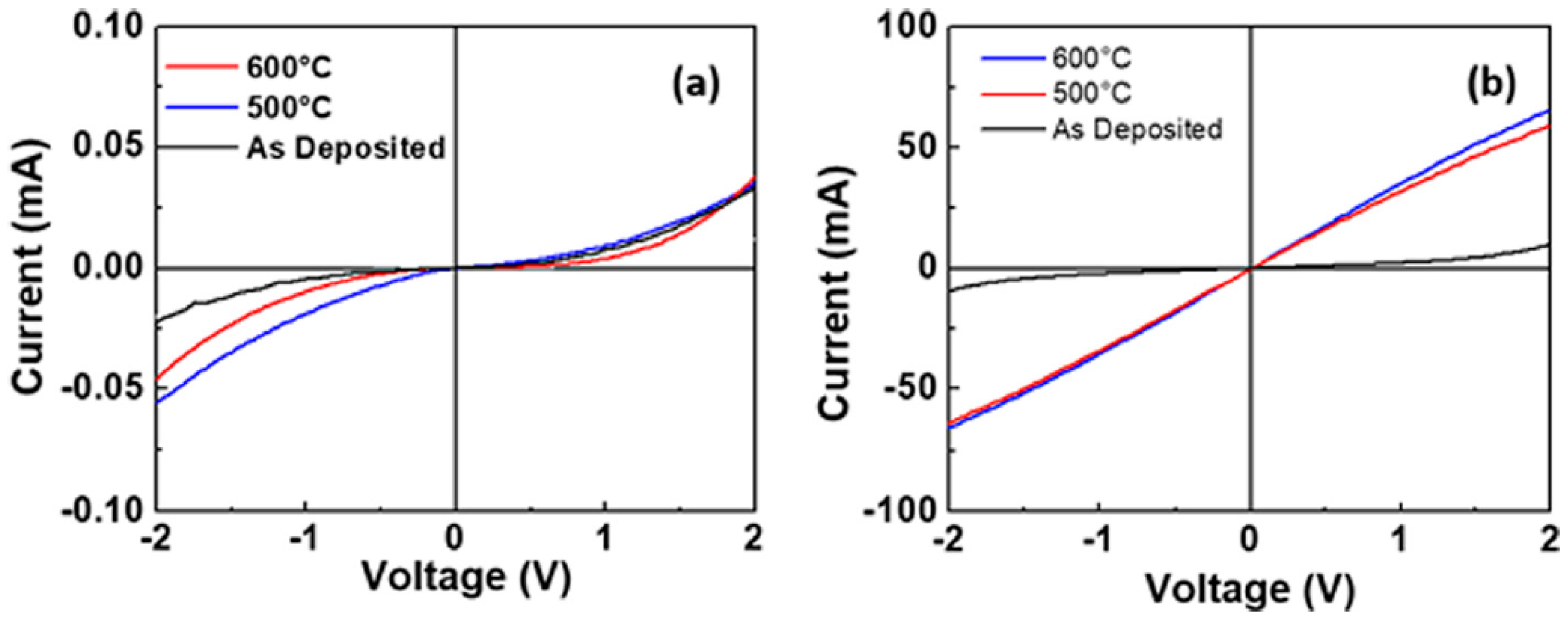
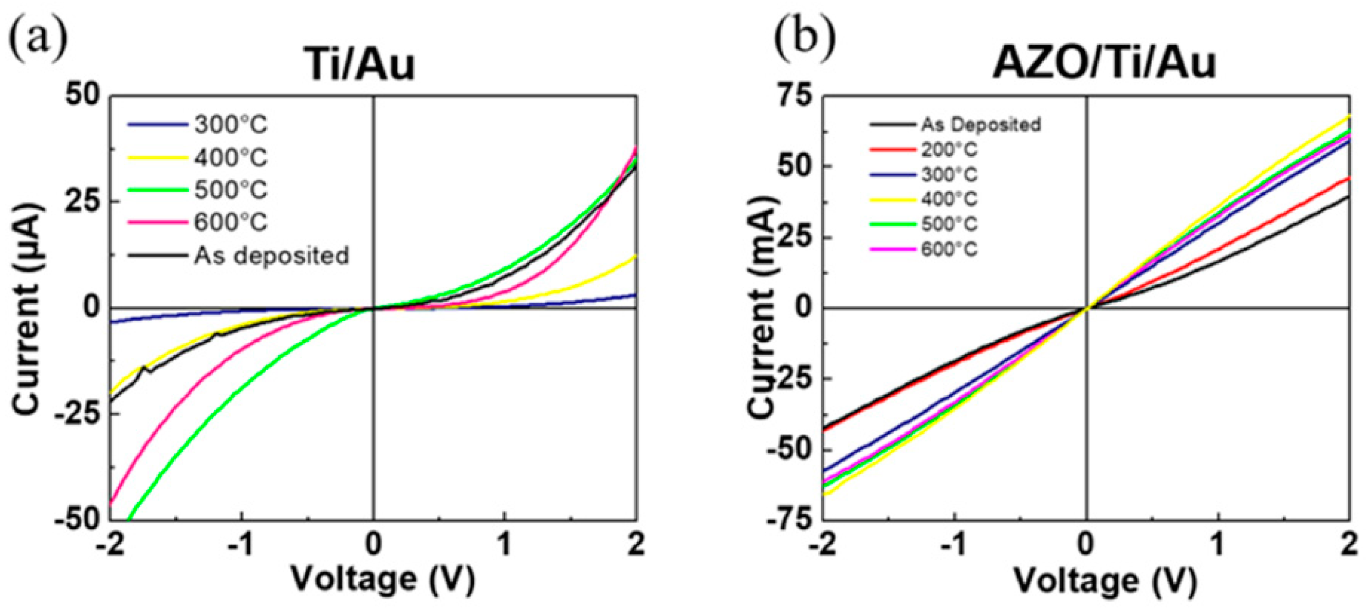
  101. Carey, P.H.; Yang, J.; Ren, F.; Hays, D.; Pearton, S.; Jang, S.; Kuramata, A.; Kravchenko, I. Ohmic contacts on n-type β-Ga2O3 using AZO/Ti/Au. AIP Adv. 2017, 7, 095313. [Google Scholar] [CrossRef]
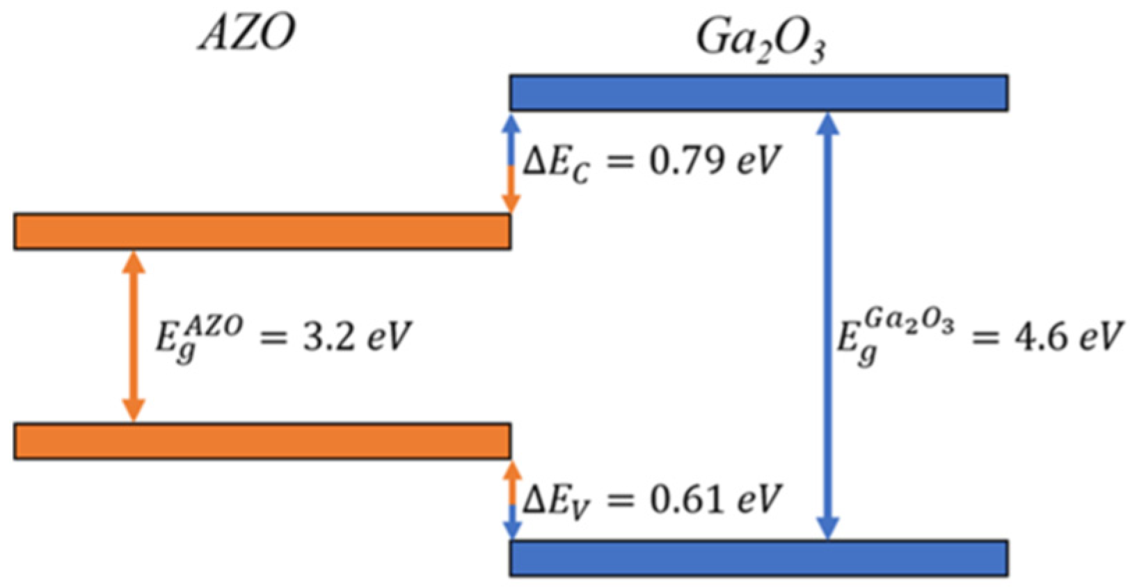
  102. Carey IVP, H.; Ren, F.; Hays, D.C.; Gila, B.; Pearton, S.; Jang, S.; Kuramata, A. Band offsets in ITO/Ga2O3 heterostructures. Appl. Surf. Sci. 2017, 422, 179–183. [Google Scholar] [CrossRef]
  103. Carey IVP, H.; Ren, F.; Hays, D.C.; Gila, B.; Pearton, S.; Jang, S.; Kuramata, A. Valence and conduction band offsets in AZO/Ga2O3 heterostructures. Vacuum 2017, 141, 103–108. [Google Scholar] [CrossRef]
  104. Kim, S.; Kim, S.J.; Kim, K.H.; Kim, H.; Kim, T. Improved performance of Ga2O3/ITO-based transparent conductive oxide films using hydrogen annealing for near-ultraviolet light-emitting diodes. Phys. Status Solidi A 2014, 211, 2569–2573. [Google Scholar] [CrossRef]
  105. Sui, Y.; Liang, H.; Chen, Q.; Huo, W.; Du, X.; Mei, Z. Room-temperature ozone sensing capability of IGZO-decorated amorphous Ga2O3 films. ACS Appl. Mater. Interfaces 2020, 12, 8929–8934. [Google Scholar] [CrossRef]
  106. Deng, Y.; Yang, Z.; Xu, T.; Jiang, H.; Ng, K.; Liao, C.; Su, D.; Pei, Y.; Chen, Z.; Wang, G. Band alignment and electrical properties of NiO/β-Ga2O3 heterojunctions with different β-Ga2O3 orientations. Appl. Surf. Sci. 2023, 622, 156917. [Google Scholar] [CrossRef]
  107. Ingebrigtsen, M.E.; Vines, L.; Alfieri, G. Bulk β-Ga2O3 with (010) and (201) surface orientation: Schottky contacts and point defects. Mater. Sci. Forum 2017, 897, 755–758. [Google Scholar] [CrossRef]
  108. Yatskiv, R.; Tiagulskyi, S.; Grym, J. Influence of crystallographic orientation on Schottky barrier formation in gallium oxide. J. Electron. Mater. 2020, 49, 5133–5137. [Google Scholar] [CrossRef]
  109. Wong, M.H.; Nakata, Y.; Kuramata, A.; Yamakoshi, S.; Higashiwaki, M. Enhancement-mode Ga2O3 MOSFETs with Si-ion-implanted source and drain. Appl. Phys. Express 2017, 10, 041101. [Google Scholar] [CrossRef]
  110. Downey, B.P.; Mohney, S.E.; Clark, T.E.; Flemish, J. Reliability of aluminum-bearing ohmic contacts to SiC under high current density. MicroElectron. Reliab. 2010, 50, 1967–1972. [Google Scholar] [CrossRef]
  111. Liu, L.; Ling, M.; Yang, J.; Xiong, W.; Jia, W.; Wang, G. Efficiency degradation behaviors of current/thermal co-stressed GaN-based blue light emitting diodes with vertical-structure. J. Appl. Phys. 2012, 111, 093110. [Google Scholar] [CrossRef]
  112. Moens, P.; Banerjee, A.; Constant, A.; Coppens, P.; Caesar, M.; Li, Z.; Vandeweghe, W.; Declercq, F.; Padmanabhan, B.; Jeon, W. Intrinsic reliability assessment of 650V rated AlGaN/GaN based power devices: An industry perspective. ECS Trans. 2016, 72, 65. [Google Scholar] [CrossRef]
  113. Li, Y.; Ng, G.I.; Arulkumaran, S.; Kumar, C.; Ang, K.; Anand, M.; Wang, H.; Hofstetter, R.; Ye, G. Low-contact-resistance non-gold Ta/Si/Ti/Al/Ni/Ta Ohmic contacts on undoped AlGaN/GaN high-electron-mobility transistors grown on silicon. Appl. Phys. Express 2013, 6, 116501. [Google Scholar] [CrossRef]
  114. Piazza, M.; Dua, C.; Oualli, M.; Morvan, E.; Carisetti, D.; Wyczisk, F. Degradation of TiAlNiAu as ohmic contact metal for GaN HEMTs. MicroElectron. Reliab. 2009, 49, 1222–1225. [Google Scholar] [CrossRef]
  115. Jeong, Y.J.; Yang, J.Y.; Lee, C.H.; Park, R.; Lee, G.; Chung, R.; Yoo, G. Fluorine-based plasma treatment for hetero-epitaxial β-Ga2O3 MOSFETs. Appl. Surf. Sci. 2021, 558, 149936. [Google Scholar] [CrossRef]
  116. Zhang, L.Q.; Shi, J.S.; Huang, H.F.; Liu, X.; Zhao, S.; Wang, P.; Zhang, W. Low-temperature Ohmic contact formation in GaN high electron mobility transistors using microwave annealing. IEEE Electron. Device Lett. 2015, 36, 896–898. [Google Scholar] [CrossRef]
  117. Hou, M.; Xie, G.; Sheng, K. Improved device performance in AlGaN/GaN HEMT by forming ohmic contact with laser annealing. IEEE Electron. Device Lett. 2018, 39, 1137–1140. [Google Scholar] [CrossRef]
Figure 1. Energy-band diagrams of metal–Ga2O3 Schottky contacts with (a) a lower Φbn and (b) an n+-doped Ga2O3 region.
Inorganics 11 00397 g001
Figure 2. Schematic illustrations of Ti/Au metallization layers on Sn-doped β-Ga2O3 with a 1 min 470 °C N2 annealing process. Reproduced from Ref. [68].
Inorganics 11 00397 g002
Figure 3. (a) Device structure, (b) equilibrium band diagram and charge profile, and (c) TLM results. Reproduced from Ref. [33].
Inorganics 11 00397 g003
Figure 4. XPS results of (a) Ga 2p3/2 and (b) Ga 3d core-level spectra from the Ti-coated (∼2.5 nm) β-Ga2O3 sample. (c) Ga 2p3/2 and (d) Ga 3d core-level spectra for the Ti/Al-coated (2/2 nm) β-Ga2O3 sample. (e) Schematic diagram of the role of Ti in the generation of oxygen vacancies. (f) Schematic of the formation process of oxygen vacancies at the interface of β-Ga2O3 and metal. Reproduced from Ref. [73].
Inorganics 11 00397 g004
Figure 5. XPS results from β-Ga2O3. (a) Normalized Ga 2p3/2 XPS spectra and Ga 3d XPS spectra from pure β-Ga2O3, (b) β-Ga2O3 after annealing in argon at 300 °C for 180 min, and (c) Ti-coated (1 nm) β-Ga2O3 after annealing in argon at 300 °C for 180 min. Black dots show experimental data, and red curves show simulated fitting curves. (d) Free energy scheme of different metal oxides. (e) Schematic diagram of the proposed oxygen vacancy model at the Ti/β-Ga2O3 interface. Reproduced from Ref. [88].
Inorganics 11 00397 g005
Figure 6. Measured contact resistivity (a), RC (b), and specific contact resistance (c) as a function of the annealing conditions. Reproduced from Ref. [90].
Inorganics 11 00397 g006
Figure 7. (a) Output characteristics of the SOG-doped MOSFET and (b,c) linear and log-scale transfer characteristics of the same device. Reproduced from Ref. [95].
Inorganics 11 00397 g007
Figure 8. Device schematic of delta-doped β-Ga2O3 MESFET. Reproduced from Ref. [32].
Inorganics 11 00397 g008
Figure 9. (a) Schematic of the fully MOVPE-grown Ga2O3 MESFET with regrown Ohmic contacts. (b) Top-view SEM image of the MESFET showing the regrown access regions. (c) Cross-sectional SEM image of the contact region showing the estimated regrowth interface. Reproduced from Ref. [36].
Inorganics 11 00397 g009
Figure 10. Typical I–V characteristics of (a) Pt/ITO and (b) Pt/Ti electrodes annealed at various temperatures. Reproduced from Ref. [99].
Inorganics 11 00397 g010
Figure 11. I–V curves of (a) Au/Ti/Ga2O3 and (b) Au/Ti/ITO/Ga2O3 contact stacks as a function of annealing temperature. Reproduced from Ref. [100].
Inorganics 11 00397 g011
Figure 12. Schematics of band offset for Au/Ti/ITO on Ga2O3 and Au/Ti on Ga2O3. Reproduced from Ref. [100].
Inorganics 11 00397 g012
Figure 13. I–V curves of (a) Au/Ti/Ga2O3 and (b) Au/Ti/AZO/Ga2O3 contact stacks as a function of annealing temperature from as-deposited samples (black lines) to 600 °C (purple lines). The 200 °C data were similar to those of the as-deposited samples, and the contact resistance decreased with temperature in the AZO-based contacts. Reproduced from Ref. [101].
Inorganics 11 00397 g013
Figure 14. Schematic of band offset for AZO on Ga2O3. Reproduced from Ref. [101].
Inorganics 11 00397 g014
Figure 15. Research progress in source/drain Ohmic contact of β-Ga2O3 devices [32,33,36,37,70,83,88,90,96,100].
Inorganics 11 00397 g015
Table 1. Physical properties and FOMs of the commonly used semiconductors.
ParametersSiGaAs4H-SiCGaNβ-Ga2O3
Bandgap, EG (eV)1.121.433.253.44.6–4.9
Breakdown field, Ebr (MV/cm)0.30.42.53.38
Electron mobility, μ (cm2 V−1 s−1)1480840010002000 (2DEG)300
Saturation velocity, Vs (107 cm/s)11.222.51.8–2
BFOM, εμEbr3114.73178462000–3000
JFOM, Ebr2Vs2/(4π2)11.827810892844
Disclaimer/Publisher’s Note: The statements, opinions and data contained in all publications are solely those of the individual author(s) and contributor(s) and not of MDPI and/or the editor(s). MDPI and/or the editor(s) disclaim responsibility for any injury to people or property resulting from any ideas, methods, instructions or products referred to in the content.

