Electric Polarization in Magnetic Topological Nodal Semimetal Thin Films

1
Institute for Materials Research, Tohoku University, Sendai 980-8577, Japan
2
Department of Physics, Nagoya University, Nagoya 464-8602, Japan
3
Center for Spintronics Research Network, Tohoku University, Sendai 980-8577, Japan
*
Author to whom correspondence should be addressed.
Condens. Matter 2018, 3(4), 43; https://doi.org/10.3390/condmat3040043
Submission received: 1 November 2018
/
Revised: 23 November 2018
/
Accepted: 28 November 2018
/
Published: 30 November 2018
(This article belongs to the Special Issue Majorana Fermions and Topological Materials Science)
Abstract
:We theoretically study the electric polarization in magnetic topological nodal semimetal thin films. In magnetically doped topological insulators, topological nodal semimetal phases emerge once the exchange coupling overcomes the band gap. Changing the magnetization direction, nodal structure is modulated and the system becomes topological nodal point or line semimetals. We find that nodal line semimetals are characterized by non-linear electric polarization, which is not observed in nodal point semimetals. The non-linear response originates from the existence of the surface states. Screening effect is self consistently included within a mean field approximation and the non-linear electric polarization is observed even in the presence of screening effect.
1. Introduction
Topological semimetals are characterized by topological numbers and topological responses [1,2,3,4]. One of the famous examples is a magnetic Weyl semimetal, which is characterized by a Chern number defined on a closed surface enclosing a nodal point called Weyl point. The Weyl points behave as a sink or source of Berry curvature, which leads to intrinsic anomalous Hall effect [5]. Magnetic Weyl semimetals exhibit a semi-quantized anomalous Hall effect as a topological response [1,6,7]. The intrinsic anomalous Hall effect in a magnetic Weyl semimetal is observed in recent experiments [8,9]. On the other hand, nodal line semimetals are characterized by a Zak phase [10]. The Zak phase is closely related to the electric polarization [11,12,13], so that we expect non-trivial electric polarization in the nodal line semimetals [3,14]. However, the electric polarization is well defined only in insulators and the applicability of the theory of polarization based on the Zak phase is ambiguous in the nodal semimetals.
In this work, we theoretically study electric polarization in magnetic topological nodal semimetal thin films. We consider magnetically doped topological insulators [15,16,17,18,19]. We assume ferromagnetic ordering of magnetic moments and introduce the exchange coupling between the band electrons and the magnetization. Once the exchange coupling overcomes the band gap, the system is brought into the magnetic topological semimetal phases [1,20]. The topological property of the band structure depends on the direction of the magnetization and the system becomes the nodal point and line semimetals by changing the direction of the magnetization [2,21,22]. There are other candidate materials of the magnetic topological semimetals [23,24], where the topology of the electronic structure depends on the magnetic structure. We numerically calculate the band structure of the topological semimetal thin films in the presence of the external potential. The screening effect is self-consistently included. We find that nodal line semimetals exhibit non-linear electric polarization, which originates from the existence of the surface states. In the nodal point semimetals, the non-linear electric polarization is not observed. Therefore, the nodal line semimetal phase is characterized by the non-linear electric polarization.
This work is organized as follows. In Section 2, we introduce model Hamiltonian which describes electronic structures of topological insulators and exchange coupling between band electrons and local magnetic moments. The screened external potential is also added. We explain the band structure of bulk systems. In Section 3, we formulate a theoretical procedure to calculate a screened potential and a self-consistently determined electric polarization. In Section 4, we show numerically calculated band structures of the bulk and slab systems. We discuss the polarization of each state in the presence of the external potential and the numerically calculated electric polarization. Conclusions are given in Section 5.
2. Model Hamiltonian
We start with the lattice model for three-dimensional topological insulators (, , and ) [25,26],
where t is a hopping parameter, a is a lattice constant, and is a mass term,
and are the Pauli matrices acting on the real spin and the pseudo-spin (orbital) degrees of freedoms. The exchange coupling between the band electrons and the local magnetic moments is written as [27]
where are exchange coupling constants and is a unit vector representing the direction of magnetization. In this work, is set on the x-z plane, as shown in Figure 1a. The first term is a usual exchange coupling and the second term originates from non-equality of the exchange coupling constants between two orbitals considered here, i.e., p-orbitals of (Bi, Sb) and (Te, Se). In magnetic topological insulators [16,18,19], Cr atoms are substituted for Bi or Sb atoms. As a result, there is the non-equality of exchange coupling between p-orbitals of (Bi, Sb) and (Te, Se). The total Hamiltonian is given as
where is the screened external potential. In the following calculation, we self-consistently include the screening effect and the detail of the numerical procedure is given in the next section.
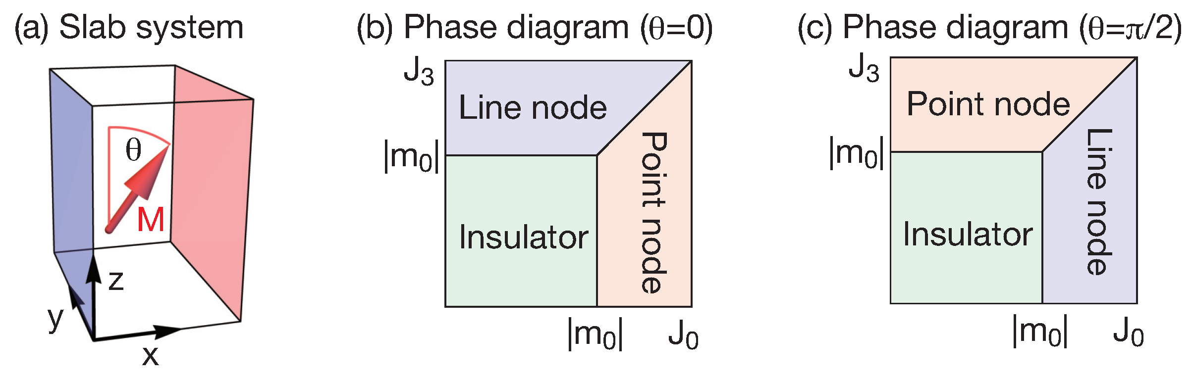
The topological phase diagram of bulk system with no-external electric field is shown in Figure 1b for and Figure 1c for . The system becomes topological semimetal phase when the exchange coupling overcomes the band gap. In the present system, both topological nodal line and point semimetal phases emerge. At , the system becomes a nodal line semimetal in and a nodal point semimetal in . At , on the other hand, the system becomes a nodal line semimetal in and a nodal point semimetal in . This means that the topological property of the electronic structure can be modulated by manipulating the magnetization direction. The topologically non-trivial band structure in nodal line semimetals is characterized by the Zak phase
where the summation is over the occupied states and is an eigenstate of the bulk Hamiltonian. In Section 4, we discuss the relation between the Zak phase and existence of surface states.
With a surface boundary for x direction as represented in Figure 1a, the wave function is written as
where and are four component spinors, and and are the system sizes along y and z directions. The Schrödinger equation becomes
We numerically diagonalize the above Hamiltonian and derive the eigenstates and the energy bands.
3. Electric Polarization Induced by the Screened Potential
We calculate electronic structure in the presence of the external electric field. The screening effect is self-consistently included within a mean field approximation by simultaneously solving the Schrödinger equation and the Poisson’s equation. Our numerical procedure is as follows. We set an initial value for the external potential as
where is the width of the slab. We derive eigenstates in the presence of the external potential. We consider the slab as multilayers of zero-thickness planes with charge density . Using the derived eigenstates, is calculated as
where is the Fermi distribution function. The electric field is calculated as
where is the permitivity and . is the induced charge density, , where is the charge density in the absence of the external potential. Here, we assume charge neutrality of the slab, or . Integrating the above electric field, the screened potential is calculated as
where we set a boundary condition for the screened potential so that the average of the screened potential is zero, = 0. We perform numerical iteration so that the screened potential converges. The strength of the screening is characterized by a dimensionless parameter defined as
Using the eigenstates with the screened potential, we calculate the electric polarization of each eigenstate,
The total electric polarization from the occupied eigenstates is written as
In the following section, we numerically diagonalize Equation (7) and self-consistently determine the electric polarization.
4. Numerical Results
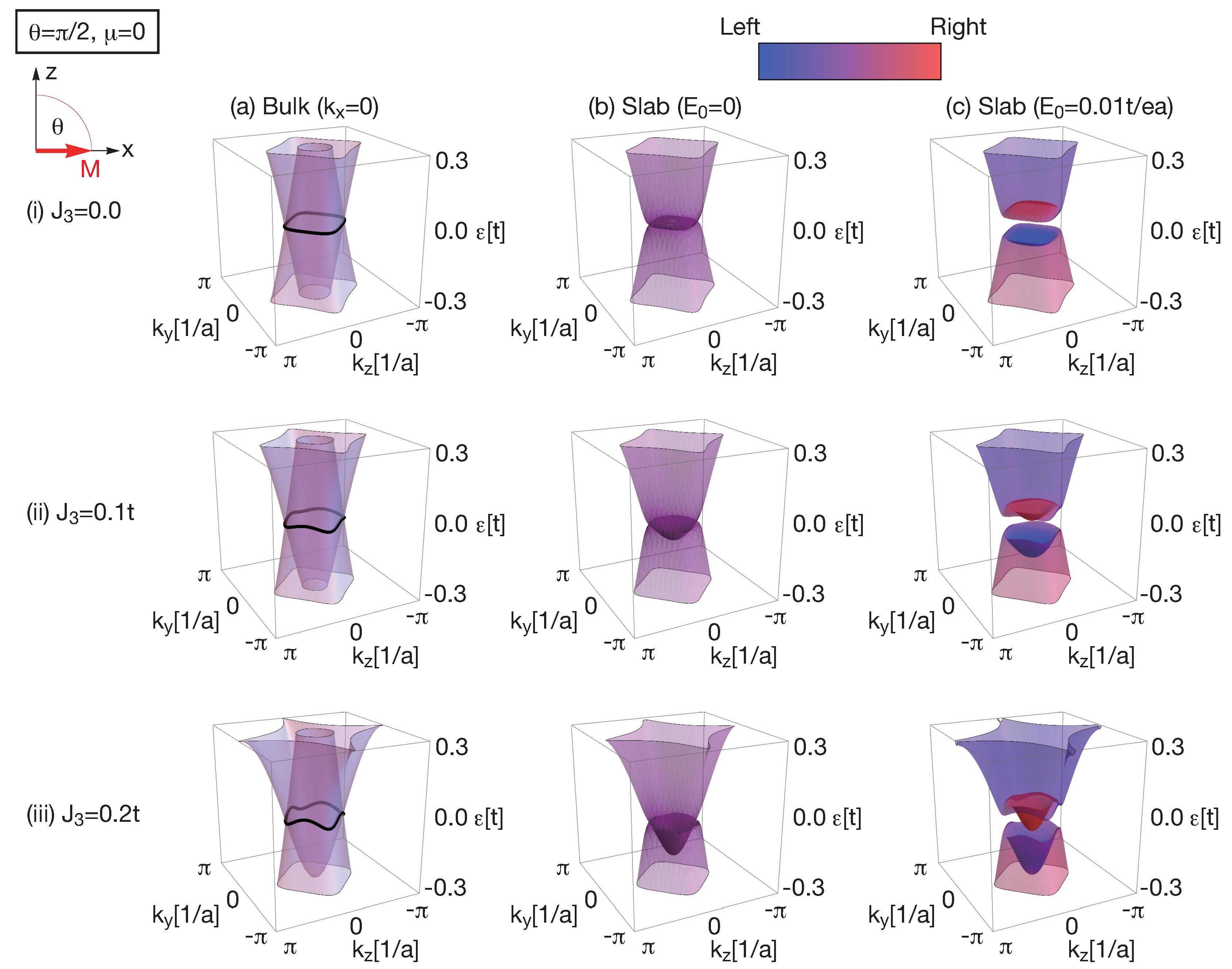
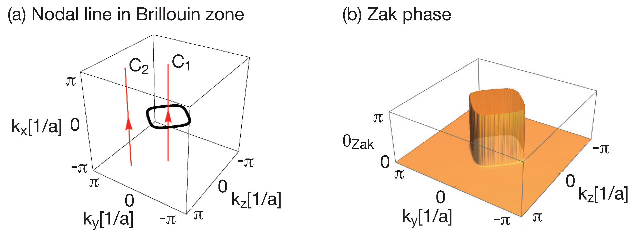
As represented in Figure 1a, we consider the open boundary condition for the x direction, and the periodic boundary condition for the y and z directions. We set the parameters as , and . First, we consider a nodal line semimetal phase, . Figure 2 shows the band structure of nodal line semimetals for several parameters. At , there is a nodal line on the plane in the bulk system. In Figure 3, we see that the Zak phase is quantized as when the integration path goes through the area enclosed by the nodal line. Otherwise, the Zak phase becomes zero. In the slab system, the wave number is discretized and we obtain subband structures. In Figure 2b, we show the lowest subbands. There are degenerate flat bands in the wave numbers enclosed by the nodal line where the Zak phase is quantized as . The flat band states are localized on the left and right surfaces. In the presence of the external potential, the degenerate flat bands are gapped, as shown in Figure 2c. The colored bar represents the polarization of each state. We see that the surface states localized on the left surface are occupied and on the right surface are empty. It means that the surface states are completely polarized and the surface electric polarization occurs. The occupied bulk states are polarized to the opposite direction so that the surface electric polarization is screened. At finite , the qualitative behavior is the same as but the band structure is slightly modified. The nodal line is not bounded on and the surface bands are bended. As a result, a larger external potential is required in order to achieve complete surface polarization compared with the flat surface bands, i.e., .
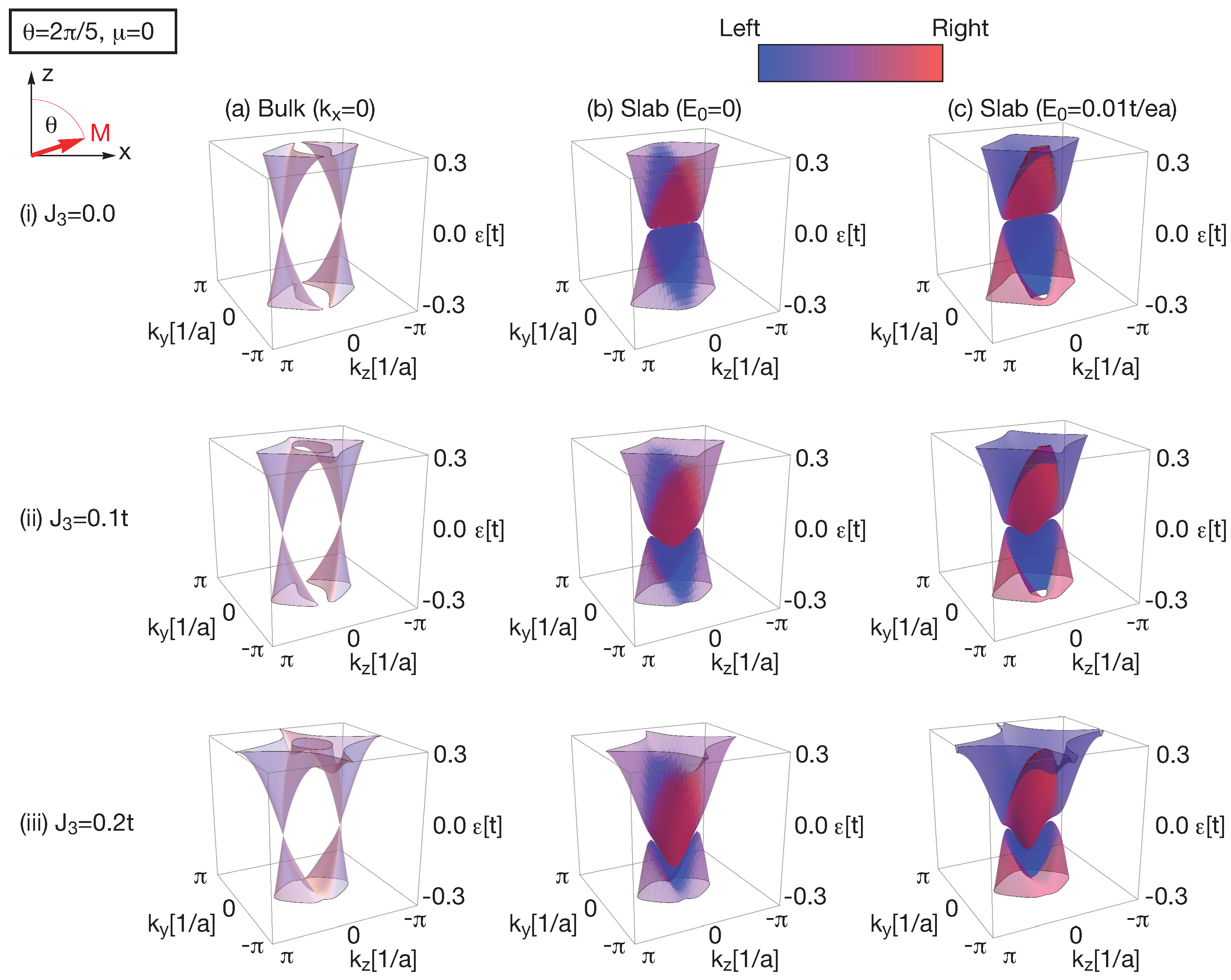
Figure 4 shows the band structure of nodal point (Weyl) semimetal phase, . When the magnetization has a finite component along z direction, the nodal line is gapped except for a pair of nodal points and the system becomes nodal point (Weyl) semimetals. In the slab system, there are chiral surface states localized on the left or right surfaces and they are seamlessly connected to the bulk states. The velocity of the chiral surface states increases with the decrease of and it becomes maximum at . In the presence of the external potential, the left surface states are pushed down and the right surface states are pushed up. Consequently, the surface electric polarization occurs but it is weak compared with that in the nodal line semimetals. In the nodal line semimetals, we observe the surface electric polarization which is proportional to the number of surface states in the sufficiently strong external potential. On the other hand, the required external potential to achieve the surface electric polarization which is proportional to the number of the surface states in the nodal point semimetals is much larger than that in the nodal line semimetals.
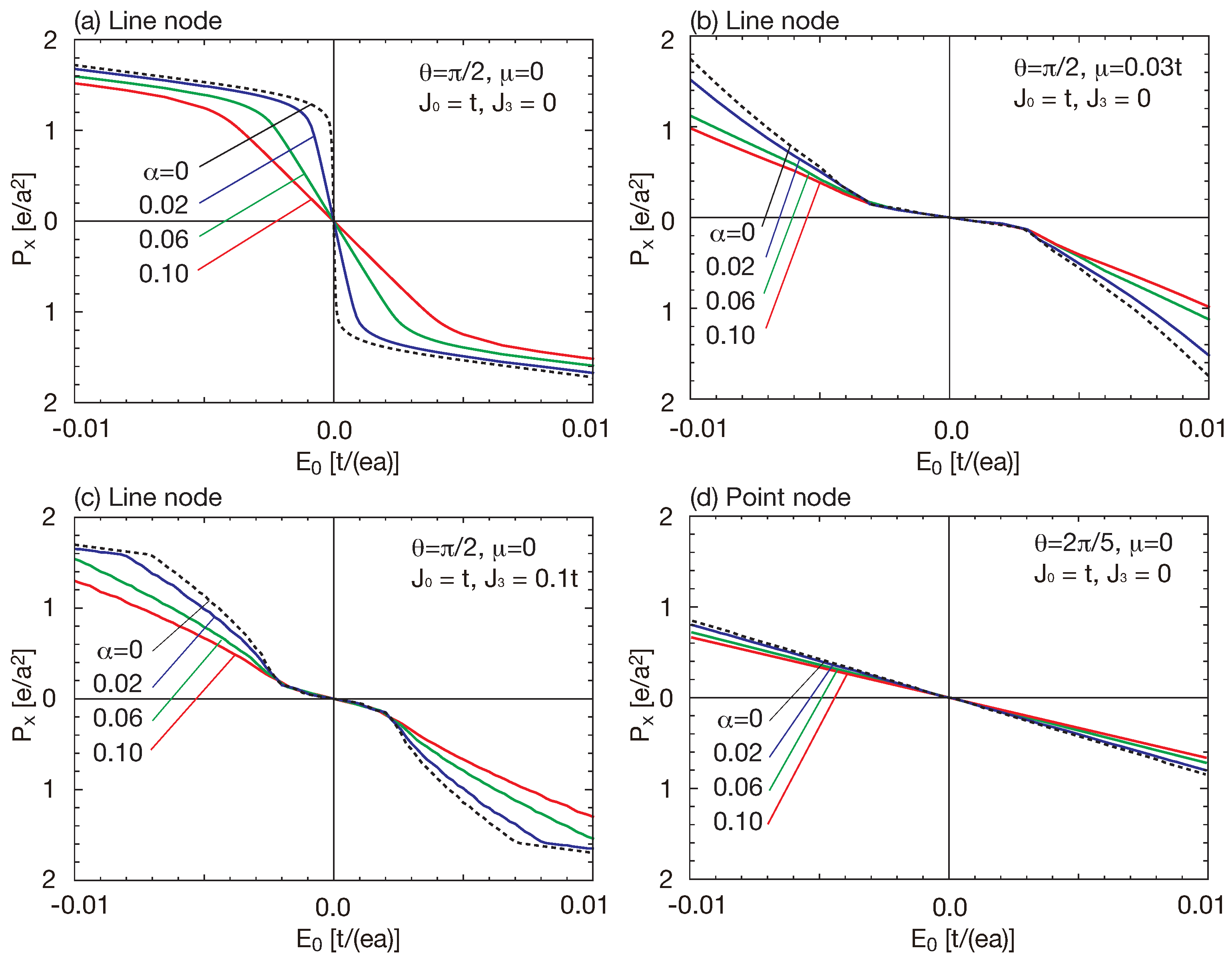
Using the self-consistently derived electronic states, we calculate the electric polarization in the slab system. Figure 5 shows the electric polarization as a function of the external electric field for several parameters. In the nodal line semimetal (Figure 5a), we see that the system exhibits non-linear electric polarization. In the absence of the screening effect , the electric polarization abruptly changes at . In the bulk limit, the electric polarization is induced by infinitesimal electric field and discontinuously changes at . However, in our numerical calculation, the electric polarization continuously changes at because of the finite size effect. In the presence of the screening effect, the step structure is broadened and the electric polarization vanishes at . However, the kink structure of the electric polarization is preserved. Figure 5b shows the electric polarization for finite chemical potential . Even in the finite chemical potential, the kink structure is observed, though the kink appears at a finite electric field. This kink structure is broadened by the screening effect. In finite term (Figure 5c), the surface bands are bended and the situation is similar to the finite chemical potential case (Figure 5b), so that the qualitative behavior is the same. In the nodal point semimetal (Figure 5d), the electric polarization is proportional to the external electric field and there is no kink structure. Therefore, the kink structure is characteristic to the nodal line semimetals and is closely related to the topological property of the system.
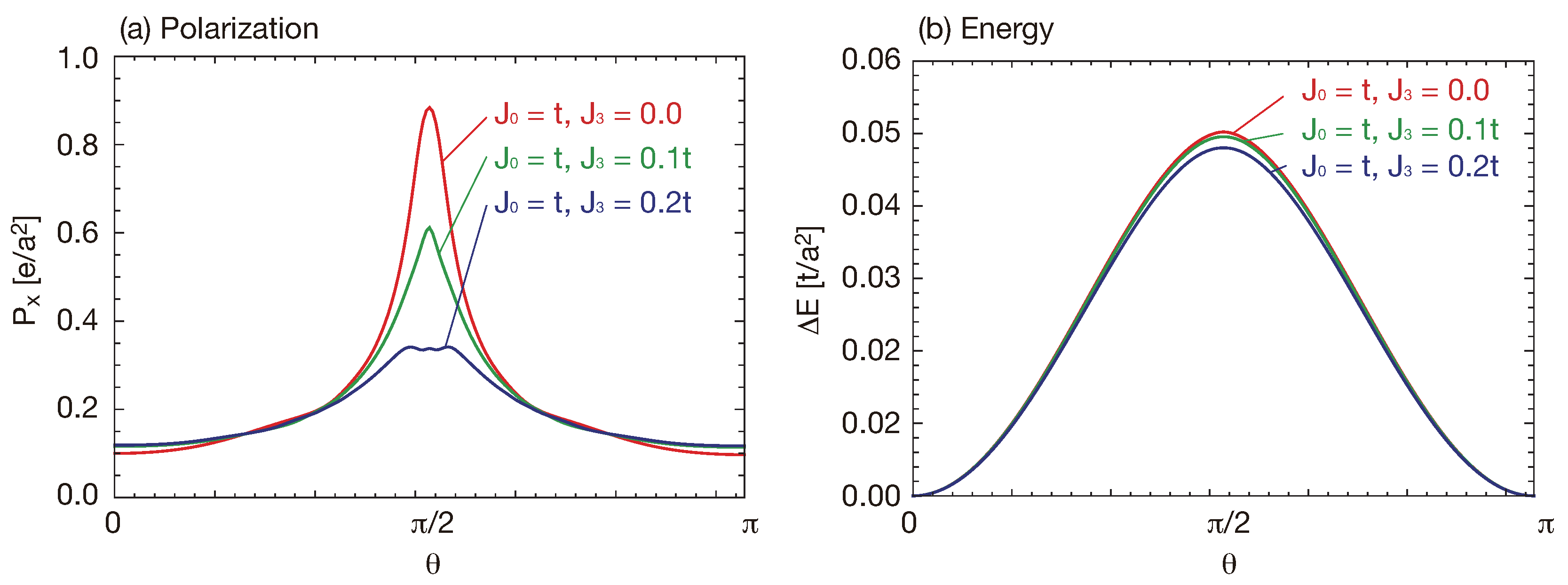
Figure 6a shows the electric polarization as a function of the angle . There are peak structures of the electric polarization at because the system becomes the nodal line semimetal at this angle and exhibits large electric polarization originating from the surface states. With the increase of , the peak value becomes smaller. This is because the surface bands are bended and the kink structure is broadened. Figure 6b shows variation of the total energy defined as
where is an eigenenergy of the slab system with the magnetization angle . The variation of the total energy also becomes maximum at and decreases away from . Unlike the electric polarization, weakly depends on and varies slowly compared with the electric polarization. This is because the electric polarization is almost determined by the property of the surface states but the variation of the total energy is almost determined by the bulk band structure. Figure 6b means that the magnetization easy axis is parallel to the surface.
5. Conclusions
We investigated the electronic structure in the magnetically doped topological insulator thin films. We found that the system becomes topological nodal semimetal phases when the exchange coupling exceeds the band gap and the topological property of the band structure is modulated by changing the magnetization direction. We calculated the electric polarization in the topological nodal semimetal thin films. We self-consistently included the screening effect and found that the nodal line semimetals exhibit non-linear electric polarization even in a finite chemical potential. This is a topological response and the nodal line semimetals are characterized by the non-linear electric polarization, which is not observed in the nodal point (Weyl) semimetals.
Author Contributions
The authors equally contributed to this work.
Funding
This work was supported by Kakenhi Grants-in-Aid (Nos. JP15H05851,JP15H05854 and JP17K05485) from the Japan Society for the Promotion of Science (JSPS) and JST CREST Grant Number JPMJCR18T2.
Acknowledgments
The authors would like to thank K. Kobayashi and Y. Araki for helpful discussions.
Conflicts of Interest
The authors declare no conflict of interest.
References
- Burkov, A.; Balents, L. Weyl semimetal in a topological insulator multilayer. Phys. Rev. Lett. 2011, 107, 127205. [Google Scholar] [CrossRef] [PubMed]
- Burkov, A.; Hook, M.; Balents, L. Topological nodal semimetals. Phys. Rev. B 2011, 84, 235126. [Google Scholar] [CrossRef]
- Ramamurthy, S.T.; Hughes, T.L. Quasitopological electromagnetic response of line-node semimetals. Phys. Rev. B 2017, 95, 075138. [Google Scholar] [CrossRef]
- Armitage, N.; Mele, E.; Vishwanath, A. Weyl and Dirac semimetals in three-dimensional solids. Rev. Modern Phys. 2018, 90, 015001. [Google Scholar] [CrossRef] [Green Version]
- Nagaosa, N.; Sinova, J.; Onoda, S.; MacDonald, A.; Ong, N. Anomalous hall effect. Rev. Modern Phys. 2010, 82, 1539. [Google Scholar] [CrossRef]
- Yang, K.Y.; Lu, Y.M.; Ran, Y. Quantum Hall effects in a Weyl semimetal: Possible application in pyrochlore iridates. Phys. Rev. B 2011, 84, 075129. [Google Scholar] [CrossRef]
- Burkov, A. Anomalous Hall Effect in Weyl Metals. Phys. Rev. Lett. 2014, 113, 187202. [Google Scholar] [CrossRef]
- Liu, E.; Sun, Y.; Kumar, N.; Muechler, L.; Sun, A.; Jiao, L.; Yang, S.Y.; Liu, D.; Liang, A.; Xu, Q.; et al. Giant anomalous Hall effect in a ferromagnetic kagome-lattice semimetal. Nat. Phys. 2018, 14, 1125–1131. [Google Scholar] [CrossRef]
- Wang, Q.; Xu, Y.; Lou, R.; Liu, Z.; Li, M.; Huang, Y.; Shen, D.; Weng, H.; Wang, S.; Lei, H. Large intrinsic anomalous Hall effect in half-metallic ferromagnet Co3Sn2S2 with magnetic Weyl fermions. Nat. Commun. 2018, 9, 3681. [Google Scholar] [CrossRef]
- Zak, J. Berry’s phase for energy bands in solids. Phys. Rev. Lett. 1989, 62, 2747. [Google Scholar] [CrossRef]
- King-Smith, R.D.; Vanderbilt, D. Theory of polarization of crystalline solids. Phys. Rev. B 1993, 47, 1651–1654. [Google Scholar] [CrossRef]
- Vanderbilt, D.; King-Smith, R.D. Electric polarization as a bulk quantity and its relation to surface charge. Phys. Rev. B 1993, 48, 4442–4455. [Google Scholar] [CrossRef]
- Resta, R. Macroscopic polarization in crystalline dielectrics: The geometric phase approach. Rev. Modern Phys. 1994, 66, 899. [Google Scholar] [CrossRef]
- Hirayama, M.; Okugawa, R.; Miyake, T.; Murakami, S. Topological Dirac nodal lines and surface charges in fcc alkaline earth metals. Nat. Commun. 2017, 8, 14022. [Google Scholar] [CrossRef] [PubMed] [Green Version]
- Zhang, J.; Chang, C.Z.; Tang, P.; Zhang, Z.; Feng, X.; Li, K.; Wang, L.L.; Chen, X.; Liu, C.; Duan, W.; et al. Topology-driven magnetic quantum phase transition in topological insulators. Science 2013, 339, 1582–1586. [Google Scholar] [CrossRef] [PubMed]
- Chang, C.Z.; Zhang, J.; Feng, X.; Shen, J.; Zhang, Z.; Guo, M.; Li, K.; Ou, Y.; Wei, P.; Wang, L.L.; et al. Experimental observation of the quantum anomalous Hall effect in a magnetic topological insulator. Science 2013, 340, 167–170. [Google Scholar] [CrossRef] [PubMed]
- Chang, C.Z.; Zhang, J.; Liu, M.; Zhang, Z.; Feng, X.; Li, K.; Wang, L.L.; Chen, X.; Dai, X.; Fang, Z.; et al. Thin Films of Magnetically Doped Topological Insulator with Carrier-Independent Long-Range Ferromagnetic Order. Adv. Mater. 2013, 25, 1065–1070. [Google Scholar] [CrossRef] [PubMed]
- Checkelsky, J.G.; Yoshimi, R.; Tsukazaki, A.; Takahashi, K.S.; Kozuka, Y.; Falson, J.; Kawasaki, M.; Tokura, Y. Trajectory of the anomalous Hall effect towards the quantized state in a ferromagnetic topological insulator. Nat. Phys. 2014, 10, 731–736. [Google Scholar] [CrossRef] [Green Version]
- Kou, X.; Guo, S.T.; Fan, Y.; Pan, L.; Lang, M.; Jiang, Y.; Shao, Q.; Nie, T.; Murata, K.; Tang, J.; et al. Scale-Invariant Quantum Anomalous Hall Effect in Magnetic Topological Insulators beyond the Two-Dimensional Limit. Phys. Rev. Lett. 2014, 113, 137201. [Google Scholar] [CrossRef] [Green Version]
- Kurebayashi, D.; Nomura, K. Weyl semimetal phase in solid-solution narrow-gap semiconductors. J. Phys. Soc. Jpn. 2014, 83, 063709. [Google Scholar] [CrossRef]
- Habe, T.; Asano, Y. Three-dimensional symmetry-breaking nontrivial topological states. Phys. Rev. B 2014, 89, 115203. [Google Scholar] [CrossRef]
- Burkov, A. Mirror Anomaly in Dirac Semimetals. Phys. Rev. Lett. 2018, 120, 016603. [Google Scholar] [CrossRef] [PubMed] [Green Version]
- Ueda, K.; Fujioka, J.; Yang, B.J.; Shiogai, J.; Tsukazaki, A.; Nakamura, S.; Awaji, S.; Nagaosa, N.; Tokura, Y. Magnetic field-induced insulator-semimetal transition in a pyrochlore Nd2Ir2O7. Phys. Rev. Lett. 2015, 115, 056402. [Google Scholar] [CrossRef] [PubMed]
- Jin, Y.J.; Wang, R.; Chen, Z.J.; Zhao, J.Z.; Zhao, Y.J.; Xu, H. Ferromagnetic Weyl semimetal phase in a tetragonal structure. Phys. Rev. B 2017, 96, 201102. [Google Scholar] [CrossRef]
- Zhang, H.; Liu, C.X.; Qi, X.L.; Dai, X.; Fang, Z.; Zhang, S.C. Topological insulators in Bi2Se3, Bi2Te3 and Sb2Te3 with a single Dirac cone on the surface. Nat. Phys. 2009, 5, 438–442. [Google Scholar] [CrossRef]
- Liu, C.X.; Qi, X.L.; Zhang, H.; Dai, X.; Fang, Z.; Zhang, S.C. Model Hamiltonian for topological insulators. Phys. Rev. B 2010, 82, 045122. [Google Scholar] [CrossRef] [Green Version]
- Wakatsuki, R.; Ezawa, M.; Nagaosa, N. Domain wall of a ferromagnet on a three-dimensional topological insulator. Sci. Rep. 2015, 5, 13638. [Google Scholar] [CrossRef] [Green Version]
Figure 1.
(a) Schematic picture of the slab system. M represents magnetization set on the x-z plane, and is an angle between the z axis and M. We assume the open boundary condition for the x direction, and the periodic boundary condition for the y and z directions. Topological phase diagram of bulk system for: (b) ; and (c) . The topological nodal semimetal phases emerge once the exchange coupling overcomes the band gap.

Figure 2.
Band structure of nodal line semimetals: (a) in the bulk system; (b) in the slab system with no E-field; and (c) in the slab system with E-field. We set the parameters as and .
Figure 2.
Band structure of nodal line semimetals: (a) in the bulk system; (b) in the slab system with no E-field; and (c) in the slab system with E-field. We set the parameters as and .

Figure 3.
(a) The black closed curve represents nodal line in the Brillouin zone. Two paths and are depicted by red arrows and give the Zak phase and 0, respectively. (b) The Zak phase calculated at fixed (). The Zak phase is quantized as in the area enclosed by the nodal line projectoed on - plane and it is zero in the other area.

Figure 4.
Band structure of nodal point (Weyl) semimetals: (a) in the bulk system; (b) in the slab system with no external potential; and (c) in the slab system with an external potential. We set the parameters as and .
Figure 4.
Band structure of nodal point (Weyl) semimetals: (a) in the bulk system; (b) in the slab system with no external potential; and (c) in the slab system with an external potential. We set the parameters as and .

Figure 5.
Polarization as a function of the external electric field for several screening strength . There are the kink structures only in the nodal line semimetals.
Figure 5.
Polarization as a function of the external electric field for several screening strength . There are the kink structures only in the nodal line semimetals.

Figure 6.
(a) The total polarization; and (b) the total energy as a function of the angle . We set , , and .
Figure 6.
(a) The total polarization; and (b) the total energy as a function of the angle . We set , , and .

© 2018 by the authors. Licensee MDPI, Basel, Switzerland. This article is an open access article distributed under the terms and conditions of the Creative Commons Attribution (CC BY) license (http://creativecommons.org/licenses/by/4.0/).
Share and Cite
MDPI and ACS Style
Ominato, Y.; Yamakage, A.; Nomura, K. Electric Polarization in Magnetic Topological Nodal Semimetal Thin Films. Condens. Matter 2018, 3, 43. https://doi.org/10.3390/condmat3040043
AMA Style
Ominato Y, Yamakage A, Nomura K. Electric Polarization in Magnetic Topological Nodal Semimetal Thin Films. Condensed Matter. 2018; 3(4):43. https://doi.org/10.3390/condmat3040043
Chicago/Turabian StyleOminato, Yuya, Ai Yamakage, and Kentaro Nomura. 2018. "Electric Polarization in Magnetic Topological Nodal Semimetal Thin Films" Condensed Matter 3, no. 4: 43. https://doi.org/10.3390/condmat3040043