Article

Plasma Actuators Based on Alumina Ceramics for Active Flow Control Applications

by
Frederico F. Rodrigues
*,
Kateryna O. Shvydyuk
,
João Nunes-Pereira
,
José C. Páscoa
and
Abílio P. Silva
Centre for Mechanical and Aerospace Science and Technologies (C-MAST), University of Beira Interior, 6201-001 Covilhã, Portugal
*
Author to whom correspondence should be addressed.
Ceramics 2024, 7(1), 192-207; https://doi.org/10.3390/ceramics7010012
Submission received: 30 October 2023 / Revised: 31 January 2024 / Accepted: 2 February 2024 / Published: 6 February 2024
(This article belongs to the Special Issue Advances in Ceramics, 2nd Edition)

Abstract

:
Plasma actuators have demonstrated great potential for active flow control applications, including boundary layer control, flow separation delay, turbulence control, and aircraft noise reduction. In particular, the material used as a dielectric barrier is crucial for the proper operation of the device. Currently, the variety of dielectrics reported in the literature is still quite restricted to polymers including Kapton, Teflon, poly(methyl methacrylate) (PMMA), Cirlex, polyisobutylene (PIB) rubber, or polystyrene. Nevertheless, several studies have highlighted the fragilities of polymeric dielectric layers when actuators operate at significantly high-voltage and -frequency levels or for long periods. In the current study, we propose the use of alumina-based ceramic composites as alternative materials for plasma actuator dielectric layers. The alumina composite samples were fabricated and characterized in terms of microstructure, electrical parameters, and plasma-induced flow velocity and compared with a conventional Kapton-based actuator. It was concluded that alumina-based dielectrics are suitable materials for plasma actuator applications, being able to generate plasma-induced flow velocities of approximately 4.5 m/s. In addition, it was verified that alumina-based ceramic actuators can provide similar fluid mechanical efficiencies to Kapton actuators. Furthermore, the ceramic dielectrics present additional characteristics, such as high-temperature resistance, which are not encompassed by conventional Kapton actuators, which makes them suitable for high-temperature applications such as turbine blade film cooling enhancement and plasma-assisted combustion. The high porosity of the ceramic results in lower plasma-induced flow velocity and lower fluid mechanical efficiency, but by minimizing the porosity, the fluid mechanical efficiency is increased.

1. Introduction

Over the years, aeronautical and aerospace industries have been interested in the research and development of new flow control techniques. The possibility of performing flow control is essential for aircraft since it is associated with several potential benefits such as performance and maneuverability enhancement, payload augmentation, fuel consumption reduction, and environmental impact attenuation [1]. For a better understanding of the impact of flow control on aircraft performance, a drag reduction of only 1% allows one to achieve an equivalent saving of 380,000 L of fuel per year in a Boeing 747 [2]. Flow control techniques are commonly classified as passive and active techniques based on their respective energy input. Passive flow control techniques are usually easier to implement and do not require external energy; however, they cannot be deactivated or adjusted during aircraft flight. Contrastingly, active flow control techniques require an external energy supply but can be adjusted during the flight and activated in real-time and unsteady flow control [2]. Although the effectiveness of passive flow control techniques has been proven, active techniques have become much more attractive due to the possibility of being activated only when and where it is necessary [3].
Considering the need for emerging technologies for active flow control, in the early 2000s, surface dielectric barrier discharge (DBD) plasma actuators were proposed as simple electronic devices capable of manipulating adjacent airflow fields. These devices generate a discharge plasma with a high electric field, which interacts with adjacent particles and creates a body force that can be used to control the flow field. Promptly, several researchers started to focus on their study due to their interesting features including fast response times, the possibility of fabrication with low-cost materials, low weight, and easy implementation even on curved surfaces. Since then, various studies have been performed demonstrating the potential of plasma actuators for active flow control such as the dynamic control of unsteady flow separation [4,5], turbulent boundary layer control [6,7], aircraft noise reduction [8], bluff body flow control [9,10], velocity fluctuation adjustment [11,12,13], drag reduction in vehicles [14,15], etc. In addition, researchers revealed that plasma actuators produce considerable thermal effects during their operation, which can be used for icing mitigation [16,17,18,19]. Bearing this in mind, several researchers focused their studies on the operation of DBD plasma actuators for simultaneous active flow control and icing accumulation prevention [20,21].
The type and thickness of the material used on the dielectric layer highly influence the performance of the plasma actuator device [22,23,24]. Furthermore, the dielectric material is the critical constituent of the actuator that is exposed to ion bombardment, ultraviolet radiation, and radical species generated during the plasma operation and, thus, it is the constituent that is more susceptible to degradation and failure [25,26]. The degradation of dielectric layers due to plasma activity was studied by Pons et al. [27]. In their work, they characterized the degradation of two polymers (polymethylmethacrylat (PMMA) and polyvinyl chloride (PVC)) exposed to discharge plasma and compared it with borosilicate glass and ceramic plates. The authors concluded that the polymers were much more vulnerable to plasma degradation than borosilicate glass and ceramic plates; after being exposed to the same conditions, they did not exhibit observable degradation. This study suggested the potential of using ceramics for plasma actuator applications. Nevertheless, no further studies have been performed in this respect. Rigit et al. [25] also studied the degradation of dielectrics; in this case, the dielectric layer was made of the standard printed circuit board, and the authors observed degradation of the dielectric surface due to the plasma actuation. The authors concluded that the dielectric is subjected to a failure rate that increases with the operation time and magnitude of the applied voltage.
Considering the importance of the dielectric material on the performance and robustness of DBD plasma actuators, it is important to propose and develop new dielectric materials with the potential for actuator efficiency and/or durability improvement. Nonetheless, few studies have been conducted with the aim of proposing new dielectric materials for plasma actuator fabrication, and most authors have only focused on the use of Kapton, Teflon, Macor ceramic, and PMMA. Rodrigues et al. [28] studied the implementation of poly-isobutylene (PIB) rubber, poly-lactic acid (PLA), and acetoxy silicon in dielectric barrier discharge plasma actuators as alternative solutions to conventional Kapton plasma actuators. It was concluded that the PLA presented several fragilities as the dielectric layer and could not operate at voltage levels higher than 10 kVpp. However, both PIB rubber and acetoxy silicon materials proved to be suitable solutions for plasma actuators’ dielectric layers, achieving higher efficiencies than the conventional Kapton actuator. Later on, in a follow-up study, Rodrigues et al. [29] proposed and studied two additional materials for a plasma actuator’s dielectric layer, i.e., poly(vinylidene fluoride) (PVDF) and polystyrene (PS). In this study, the authors concluded that the PVDF did not produce good indicators for flow control applications since it could not induce velocities with magnitudes above 0.5 m/s and operate at voltages higher than 8 kVpp without failing. In the same line of thought, Nunes-Pereira et al. [30] proposed the utilization of Cirlex as a dielectric barrier in plasma actuators. In this work, the authors verified that Cirlex consumed less power than Kapton to generate a higher induced flow velocity of approximately 3.4 m/s for input voltages of 11 kVpp and 24 kHz. Considering these findings, it was highlighted that Cirlex is a suitable alternative for Kapton to fabricate DBD plasma actuators for flow control with improved performance.
In this context, considering the drawbacks of polymeric dielectrics, it is important to propose alternative types of materials for dielectric barrier layers of plasma actuators. In our recent work [31], we demonstrated the potential of ceramic materials to extend the lifetime and robustness of DBD plasma actuators and, as a follow-up, in the current work, we aim to analyze the influence of the ceramic material’s porosity and compare the behavior of a ceramics-based actuator with a conventional Kapton actuator. For that purpose, alumina-based ceramic composites were produced and experimentally tested as plasma actuator dielectric layers. Alumina-based ceramics were selected based on their features and the variety of reported applications in aeronautical and aerospace fields [32]. Moreover, the chosen alumina ceramics are based on common raw materials and obtained through a simple fabrication process. The ceramic samples were characterized in terms of the micro-structure, electrical parameters, and plasma-induced flow analysis and compared with a conventional Kapton-based actuator.

2. Materials and Methods

In the current work, two samples of MgO-Al2O3 were fabricated and applied as dielectric barriers for plasma actuators. Commercial aluminum oxide powder (Al2O3) supplied by Acros Organics(Geel, Belgium) and magnesium oxide powder (MgO) produced by Alfa Aesar (Ward Hill, MA, USA) with high purity (wt.%: 99 and wt.%: 96, respectively), were used as starting materials. In the manufacturing of the first alumina sample, hereinafter designated as “MA1”, the raw powders were milled for 3 h at 500 rpm in a high-energy planetary mill model “Pulverisette 6” distributed by Fritsch (Idar-Oberstein, Germany) using grinding bowls with a 250 mL capacity. The second alumina sample, hereinafter designated as “MA2”, was fabricated using the same method but with an optimized fabrication approach that included a milling time of 6 h instead of 3 h. The analysis of the particle size of the mixture—based on the laser diffraction principle with a multifunctional particle characterization tool, Beckman, model “Coulter LS-200” (Brea, CA, USA)—was conducted to control the particle size distribution. In addition, alumina balls of 1 mm diameter were added to the powder mixtures using isopropyl alcohol as a medium in a powder/alcohol/balls ratio of 1/1/2 (100 g of powder, 100 g of isopropyl alcohol, and 200 g of balls to provide the homogenization of the mixture). The milling process was performed with cycles of 30 min with intervals of rest to ensure that the mixture would not overheat inside the grinding bowls. Afterward, the mixture was dried at 50 °C for 24 h in the air using the oven model “Carbolite NR200-F” (Hope Valley, UK) to ensure complete evaporation of the isopropyl alcohol and, in due course, sieved with a vibratory shaker machine, model “Retsch AS200” (Haan, Germany) with a 63 µm mesh so that the collected fine particles would be free of unintended agglomerates and impurities. The uniaxial pressing technique was adopted in a universal testing machine, model “Instron 8800” (Canton, MA, USA) with an electromechanical actuator capacity of 100 kN and using rectangular dies of high-strength steel measuring 60 × 60 mm. The sintering process was carried out in the air in the oven model “Termolab MLR” (Agueda, Portugal) and consisted of a heating rate of 5 °C/min to the sintering temperature of 1600 °C with 120 min dwell time. To finalize, optimization grinding and polishing procedures were performed using the polishing machine model “Struers DAPV” (Ballerup, Denmark) with silicon carbide paper.
For the analysis of the fabricated ceramics, thermal etching was conducted for microstructure contrasting for 30 min at 1440 °C, considering heating and cooling rates of 10 °C/min. Moreover, the fabricated ceramic surfaces were gold-sputtered with a turbomolecular pump coater model “Emitech K550 Gold Sputter Coater, Quorum Technologies” (Lewes, UK) and, finally, scanning electron microscopy (SEM) measurements were performed with a scanning electron microscope model “Hitachi S-2700” (Kansai, Japan) by applying an accelerating voltage of 20 kV.
The apparent porosity of the fabricated ceramics was quantified following the ASTM C-20-00 [33] standard test methodology, using deionized water and the single-pan analytical balance model “Oertling” (London, UK). For the apparent porosity estimation, bar specimens were used to measure the dry weight (D), saturated weight (W), and suspended weight (S). After obtaining the above-mentioned quantities, the exterior volume (Ve) was determined by subtracting the suspended weight (S) from the saturated weight (W). Then, the apparent porosity (Pa (%)) was quantified by dividing the difference between the saturated weight W and dry weight (D) for the exterior volume (Ve), as described in Equation (1).
P a = W D V e × 100 %
For a comparison of the two alumina ceramic dielectrics, a Kapton dielectric layer was also produced by overlapping several Kapton tape layers until a 5 mm thick layer (the same thickness as the fabricated alumina ceramic plates) with 60 × 50 mm dimensions was obtained. The dielectric layers produced (MA1, MA2, and Kapton) were then used to obtain plasma actuators by adding two electrodes to them, one exposed with a 10 mm width and one embedded with a 20 mm width. Both electrodes were made of copper tape with 80 μm thickness and the electrodes were asymmetrically mounted with co-aligned edges with no gap between them in such a way that the plasma spanwise length was 30 mm, as is shown in Figure 1.
The actuators were operated using a high-voltage power source, model PVM 500, manufactured by Information Unlimited (Amherst, NH, USA), which is capable of producing voltages of up to 20 kV AC peak-to-peak with frequencies within the range of 20 kHz to 50 kHz. The supplied signals were monitored using an analog-to-digital converter model 𝑃𝑖𝑐𝑜𝑆𝑐𝑜𝑝𝑒 5443𝐴 (St Neots, UK) coupled to a high-voltage probe model “Secondary Ignition Pickup”. The electric current method and the electric charge method, commonly reported in the literature [34,35], were used for electrical characterization. For applying the electric current method, a thermal stable metal film resistor of 100 Ω with 1% tolerance was used, placed in series with the actuator, while for the electric charge method, the resistor was substituted by a ceramic capacitor with 10 nF of capacitance and 10% tolerance.
Pitot tube measurements were also performed in order to evaluate the induced flow velocities and estimate the actuators’ mechanical efficiency. For that purpose, a stainless-steel Pitot tube, model “167-6”, with an inner diameter of 1.19 mm and an external diameter of 3.18 mm was used coupled to a micromanometer, model Extech HD 350 (Kent, UK) with a resolution of 0.01 m/s and an accuracy of 1%FS. The horizontal distance between the junction of the electrodes and the Pitot tube was 15 mm, as shown in Figure 1. This distance was chosen in accordance with other works reported in the literature, which have demonstrated that this is the region where the maximum induced flow velocities are found [36,37]. In addition, we verified that at this distance, the Pitot tube is close enough to capture the induced flow velocity well but far enough away to avoid any contact with the plasma area, as is demonstrated in Figure 1b. As we see in this figure, the Pitot tube is quite close to the plasma region but far enough away to avoid any arc formation even at 18 kVpp, which was the highest voltage level tested in the current work. The distance between the vertical measurement points was measured using a caliper rule with a resolution of 0.01 mm.

3. Results

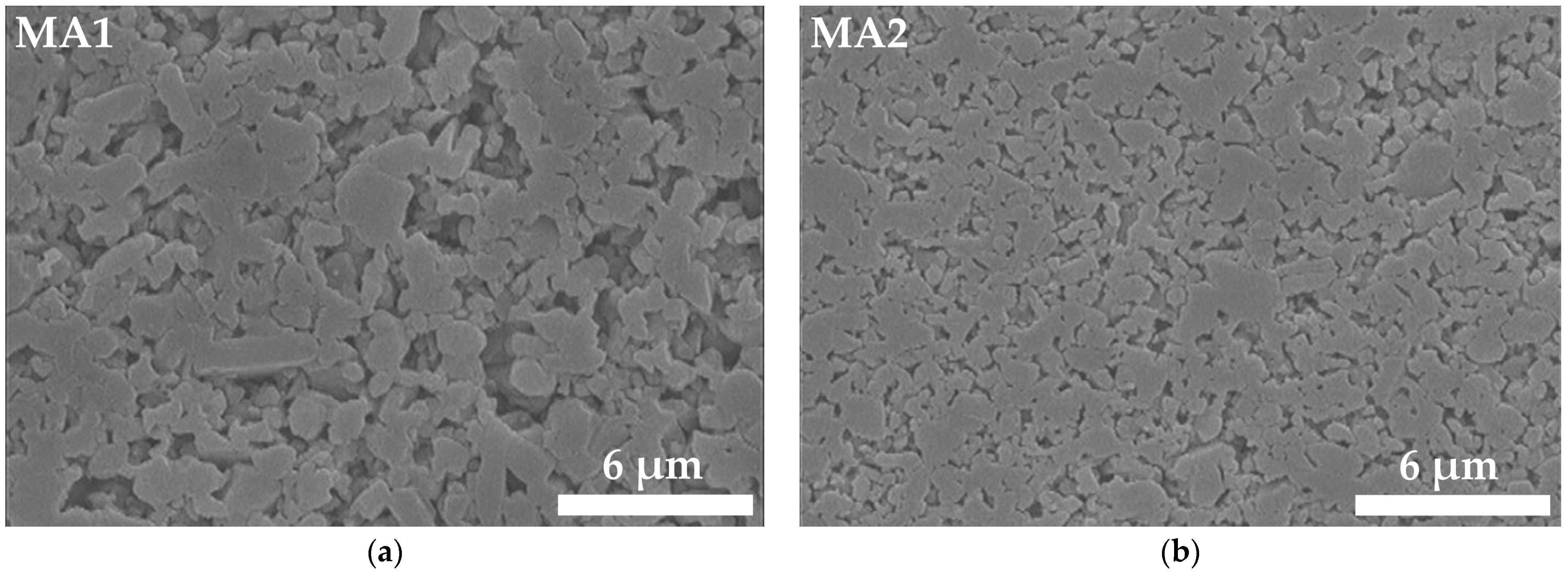
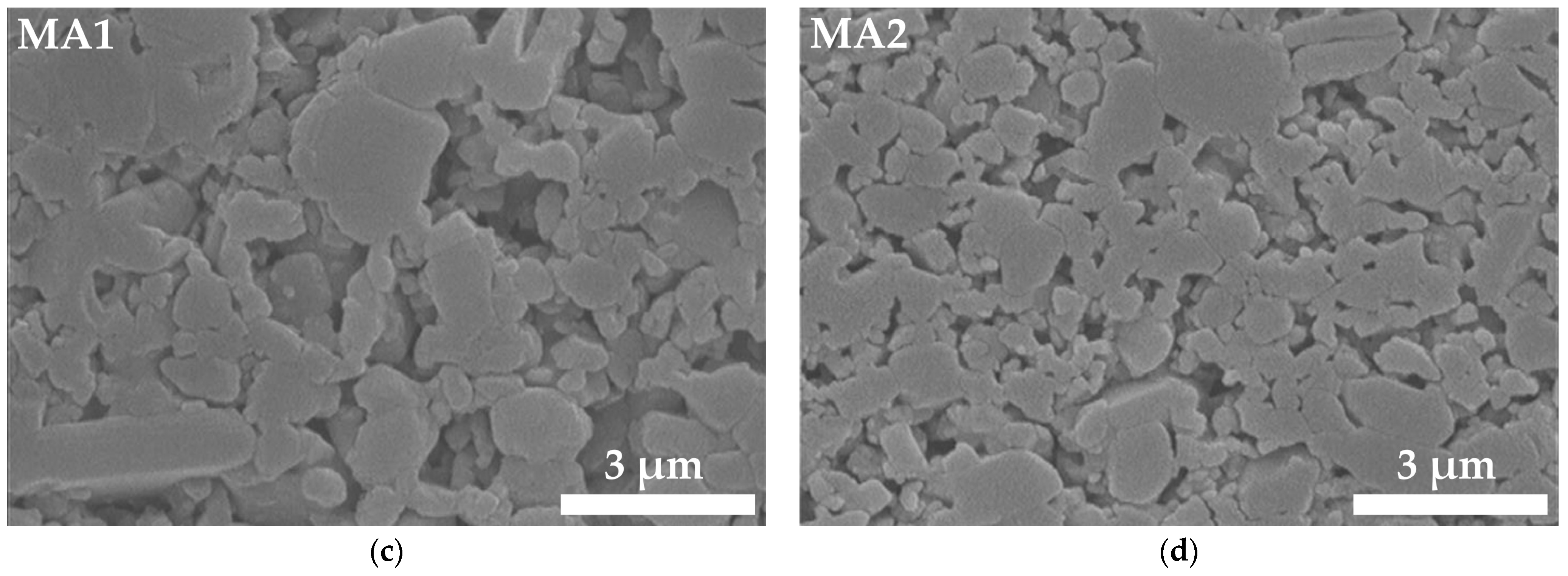
3.1. Microstructure of the Fabricated Ceramics

As explained in the previous section, in order to understand the influence of the ceramic porosity on the plasma actuator performance, two alumina samples were fabricated with different milling times (MA1—3 h; MA2—6 h). Our aim was to obtain two ceramic plates with the same composition but different porosity contents in order to analyze their impact on the plasma actuator performance. The SEM images are presented in Figure 2. This figure illustrates the differences between the two alumina ceramics produced, making it clear that MA1 presents a higher content of porosity and pore interconnectivity, fewer points of contact among grains, and higher microstructure heterogeneity, while MA2 shows a greater compaction degree and higher densification of the material. Moreover, both alumina micrographs show a multiformity of grains, both in size and geometry. It is possible to observe some grains more elongated and longer with a chord length of <2 μm, others more circular and smaller with a chord length of <1 μm, and some uneven ones with variable chord lengths. However, in general, we may conclude that the grain sizes of both MA1 and MA2 samples do not exceed 3 μm chord length.
Additionally, both ceramic composites MA1 and MA2 present an irregular shape of the grains and high porosity, which indicate an incomplete sintering [38,39]. This means that by increasing the milling time of the MA2 sample, we effectively decreased the particle size of the MA2 mixture and, in turn, increased the atomic diffusion. Thus, to obtain an even more dense material, the sintering time can be increased, which will result in higher diffusivity and a better-defined crystal structure. Ultimately, the results demonstrate that we effectively produced two ceramic samples with different grain sizes, as desired.
In addition, the apparent porosity of both fabricated dielectric plates was estimated as described in the previous section. The results obtained confirmed a relatively high and high porosity of both alumina samples, i.e., MA1 and MA2, respectively. For MA1, an apparent porosity of approximately 34.62 ± 4.6% was obtained, while MA2 resulted in an apparent porosity of approximately 7.03 ± 0.9%. The data confirmed again that the different milling times allowed us to obtain two samples with different porosities, with MA1 presenting a significantly higher apparent porosity than the MA2 specimen. After analyzing the two microstructures of the fabricated ceramic plates, they were mounted as a surface dielectric barrier discharge device. Therefore, in the next subsections, the behavior of the material in terms of electrical characteristics and plasma-induced flow performances as a surface dielectric barrier discharge plasma actuator is studied.

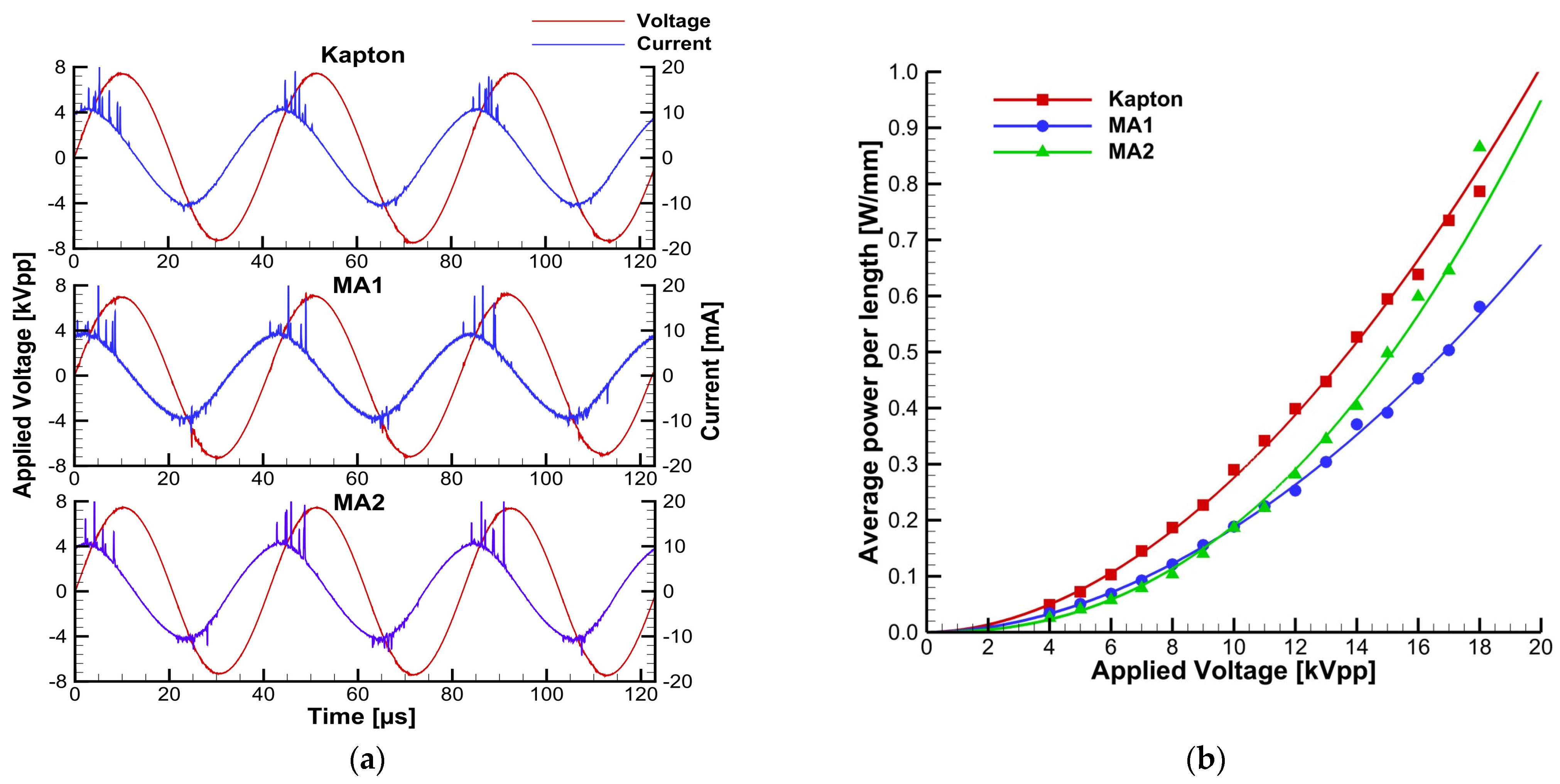
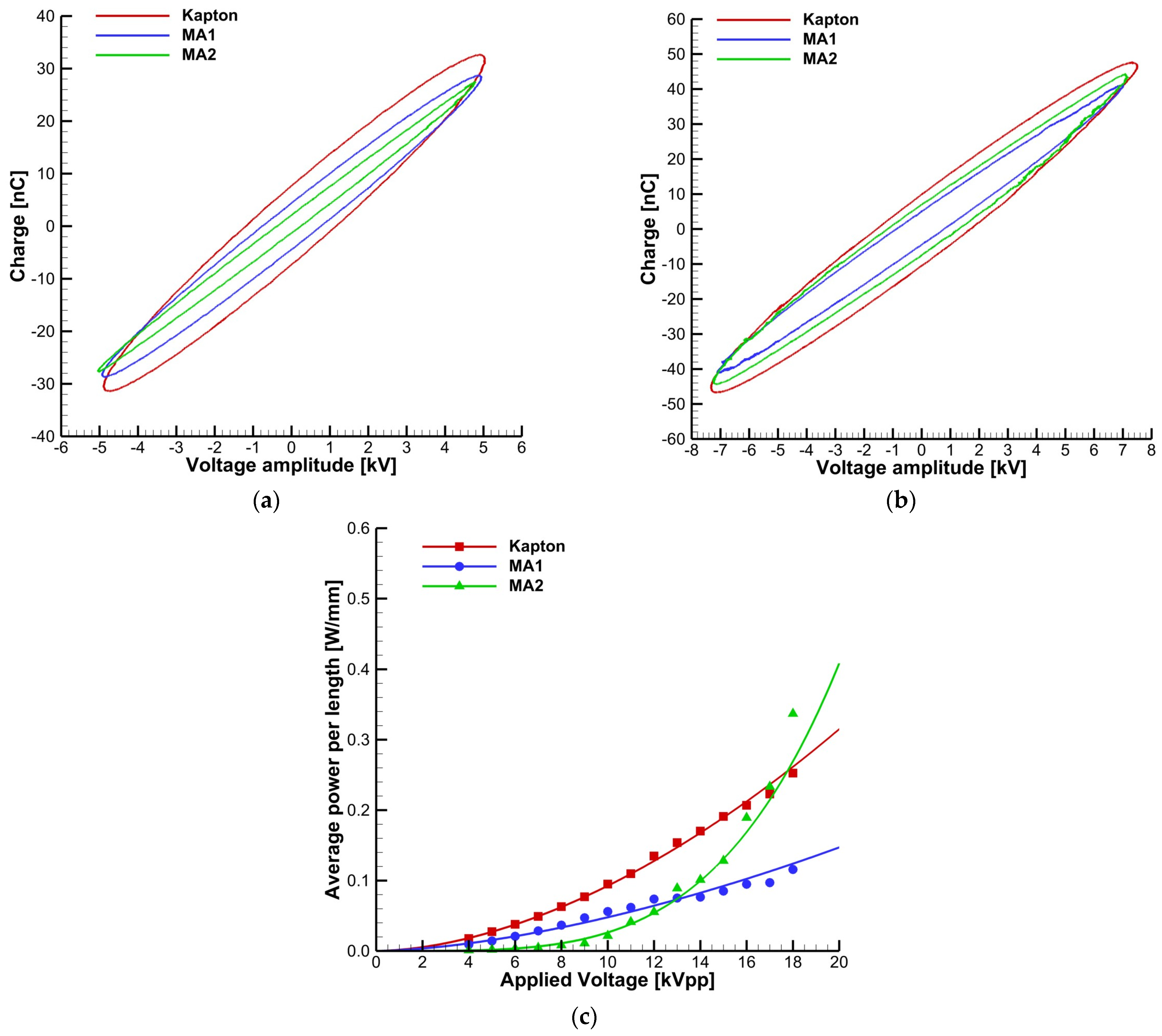
3.2. Plasma Actuators Electrical Characterization

To perform electrical characterization, the electric current method and electric charge method were applied. The electric current method allowed us to obtain the current and voltage waveforms and, with that, the average electrical power consumed was quantified for different applied voltage levels as described in the following equation:
P ¯ = 1 n T 0 n T V t · I t d t
where n is the number of cycles analyzed, T is the period, V(t) is the voltage function, and I(t) is the current function. The current and voltage waveforms are presented in Figure 3a while the average power consumption results are shown in Figure 3b.
The current and voltage signals were acquired with a resolution of 14 bits at a sampling rate of 125 MS/s, which confer to the results an uncertainty lower than 2%. As we can see from Figure 3a, the voltage and current waveforms of the tested plasma actuators present the common behavior expected for a dielectric barrier discharge device, with the current leading the voltage with a displacement of approximately 90°. In addition, as expected, the current waveforms present the high-frequency current spikes superimposed on the lower-frequency current signal, which are generated by the fast impedance changes due to the formation of each micro-discharge. From Figure 3b, we verified that, at up to 17 kVpp, both alumina-based dielectrics present lower power consumption than the conventional Kapton actuator. However, for voltage levels higher than 17 kVpp, the measurements indicate that the power consumed by the MA2 actuator surpasses the power of the Kapton actuator. We can observe that the MA2 sample presents a behavior quite similar to MA1 for lower voltage levels, i.e., up to 10.2 kVpp, but for higher voltage levels, the power consumption is closer to the Kapton values. We should mention that this voltage level is close to the breakdown voltage of alumina-based actuators, which was approximately 10 kVpp, while for Kapton, the breakdown voltage was close to 11.3 kVpp. The breakdown voltage found for the alumina-based actuators is in agreement with the work of Lindner et al. [40] who reported a breakdown voltage of 8.2 kVpp for an actuator with a 2.4 mm thickness. As expected, the breakdown voltage found for our alumina-based actuators is larger since we are using a thicker dielectric layer, but not excessively larger since we are operating the actuator with a higher frequency level. Moreover, it is clear that the porosity of the material affects the power consumption and the electrical behavior of the device. Lastly, by comparing the values obtained for the MA1 and MA2 samples, we may conclude that the decrease in the ceramic plate porosity will lead to an increase in power consumption.
It is important to emphasize that, as explained by Synek et al. [41], the determination of power consumed in the discharge is very challenging and its accurate quantification is quite difficult since parasitic energy losses such as losses in dielectric, connection wires, humidity, and radiation of the electromagnetic waves into open space may affect its estimation. Therefore, to avoid erroneous interpretations and complete the electrical characterization, the electric charge method was also applied. The charge was quantified as the product of the capacitor capacitance and the voltage across the capacitor placed in series with the actuator. After obtaining the charge variation over time, almond-shaped charge–voltage curves were obtained. These curves show the evolution of the actuator charge during the voltage cycle, and the area inside the curve divided by the period provides the power consumption of the device. The charge–voltage curves are presented in Figure 4a for a constant applied voltage of 10 kVpp and Figure 4b for a constant applied voltage of 15 kVpp (frequency of 24 kHz). The curves presented in Figure 4 are the result of the average of five cycles. The power consumption was quantified for all tested voltage levels and the results are presented in Figure 4c.
From the analysis of Figure 4a,b, we can observe that for an applied voltage of 10 kVpp, the voltage value is very close to the breakdown voltage and the curves are quite narrow, mainly for the ceramic’s dielectrics, because still there is no active discharge, as explained in Synek et al. [42]. However, as we can see, there is already a measurable area inside the curves, which should be related to the power losses as dielectric heating. This is in accordance with the results obtained by the electric current method, which also exhibited a few watts of power consumed even at levels below the breakdown voltage (between 4 kVpp and 10 kVpp). As explained by Roth et al. [43], dielectric heating increases with the applied voltage and frequency; thus, since we are using a high frequency (24 kHz), we should expect considerable power dissipated as dielectric heating. Moreover, our results of power below the breakdown voltage are in the range of the estimations performed by Roth et al. [43] who reported approximately 2.5–3 watts of energy dissipated as heat for an applied voltage of 2 kV and a frequency of 13 kHz. Since we used a high frequency and thermal power losses increased, we also did not observe the linear power consumption as a function of voltage amplitude reported by Lindner et al. [40], but instead a polynomic function as described in Wilde et al. [44]. When we increase the applied voltage to 15 kVpp (Figure 4b)), we observe that the area inside the figures increases, and the figures become wider and more similar to the traditional almond-shaped figures. The results presented in Figure 4a,b clearly corroborate the power consumption results achieved by the electric current method with the Kapton, showing a wider charge–voltage curve with a larger area inside. In addition, for lower voltages, we observe that MA1 presents a wider curve than MA2, but with an increase in the voltage level, this scenario inverts, indicating a stronger discharge plasma formation by the MA2 sample.
By using the charge–voltage curves, the capacitance of the three different devices without discharge was also quantified using the same method as that reported by Synek et al. [42]. In this method, we used the Q-V plots for different voltages to obtain the line connecting the extremal points of the curve, where Q reaches the maximum or minimum value, and the capacitance is given by the slope of that line. The measurement was performed for voltages between 4 kVpp and 8 kVpp, and the average capacitance was quantified. From this analysis, we found that the Kapton actuator has a capacitance of 6.89 ± 0.06 pF, MA1 5.94 ± 0.01 pF, and MA2 has a capacitance of 5.47 ± 0.01 pF. From the literature, we know that the dielectric permittivity of Alumina is considerably larger than the dielectric permittivity of Kapton (the dielectric permittivity of alumina is approximately 9.2 [45] and Kapton is approximately 3.5 [46]) and, therefore, we were expecting to obtain a smaller capacitance for the Kapton actuator than for the alumina-based actuators. This can be justified by several reasons. The reason that most influenced the results was the manufacturing method used for producing the ceramic plates. As mentioned, the tested ceramics were manufactured by a conventional sintering process, which means that the specimen’s geometry will depend on the microstructure and, thus, we cannot fully control the accuracy of the thickness dimension during the sintering process. Having even the lowest porosity content in the ceramic specimens influences the thickness across the length of the specimen plate. Therefore, we tried to confirm the thickness of the ceramic plates by measuring them with a pachymeter and observed thickness variations between 4.92 and 5.41 mm on the edges of the plates. Keeping this in mind, we conclude that the actuator electrodes are positioned in a region where the thickness of the dielectric is slightly greater than 5 mm, and this explains the smaller capacitance of the alumina-based ceramic actuators in comparison to the Kapton actuator. Since the actuators were mounted manually, human error in the positioning of the electrodes may also influence the capacitance of the plasma actuator arrangements.
By comparing the plot obtained by the electric current method (Figure 3b) with the electric charge method (Figure 4c), we can observe that the power values are lower when the measurements are performed using the electric charge method. This is in line with the findings of Ashpis et al. [34] who reported that measurements of average power consumption using the shunt resistor may provide 80% larger values than using the monitor capacitor method. In our case, the percentage difference between the two measurements is lower, which demonstrates better consistency between the two methods, but still, we confirm that the average power measured with the monitor capacitor method is considerably smaller than that obtained using the shunt resistor method. In addition, we should emphasize that the trend observed in the power consumption computed through the electric current method is the same obtained now by the electric charge method. As shown in Figure 4c), at up to 17 kVpp, Kapton is the actuator that presents larger power consumption, but for higher voltages, it is surpassed by MA2. At up to 12 kVpp, the MA2 power consumption values are slightly lower but close to the power consumption of MA1. With the applied voltage growth, the power consumption of MA2 increases faster than the MA1, as was also observed by the electric current method. The same behavior is observed when we compare MA2 to Kapton, which, with the increase in applied voltage, presents a smoother power consumption increase than MA2. Because of that, we see that for applied voltages above 17 kVpp, the power consumption of MA2 surpasses the power consumed by the Kapton actuator. Therefore, we may conclude that both measurement methods are in accordance and the results obtained are consistent between the two independent methods.

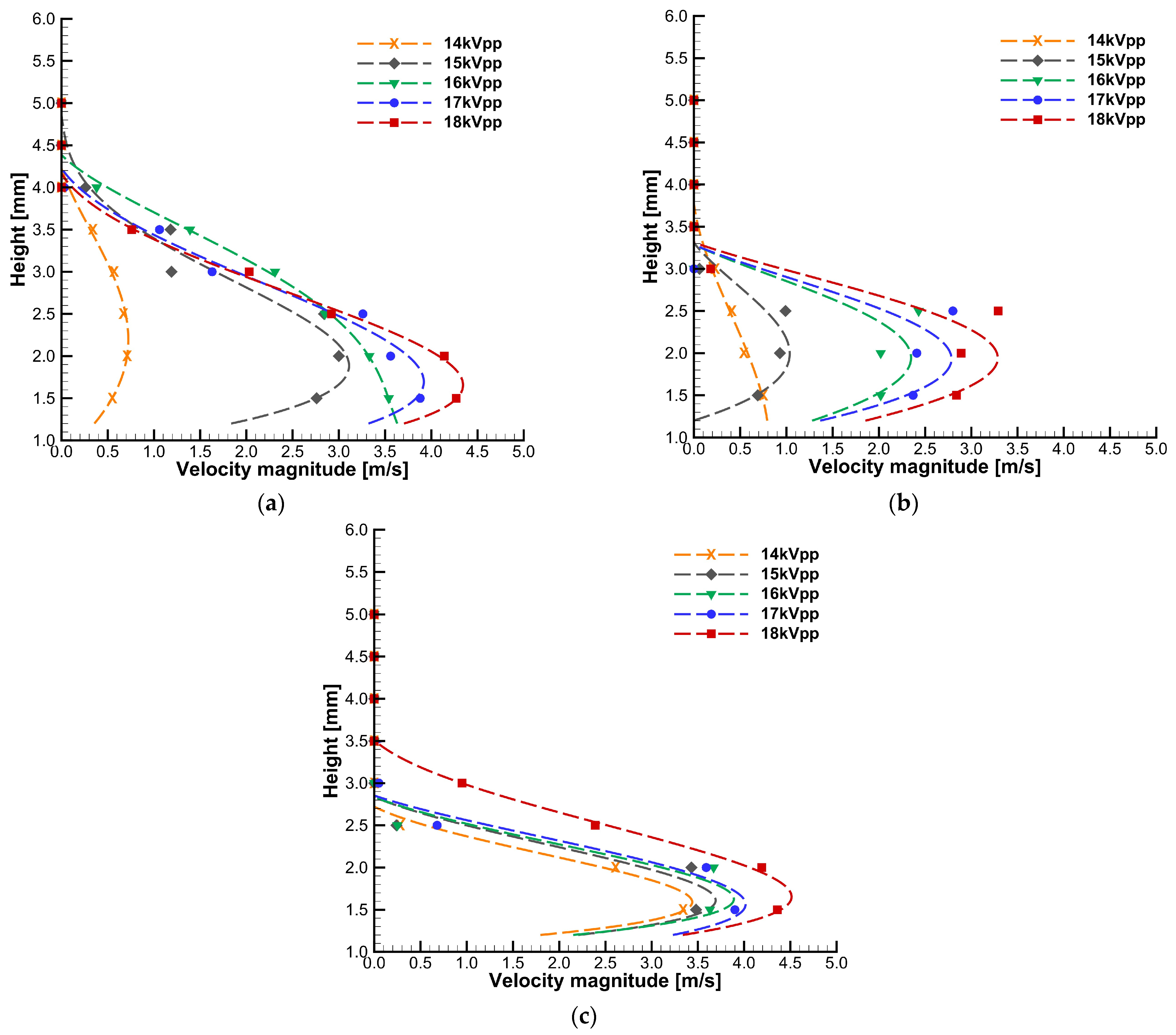
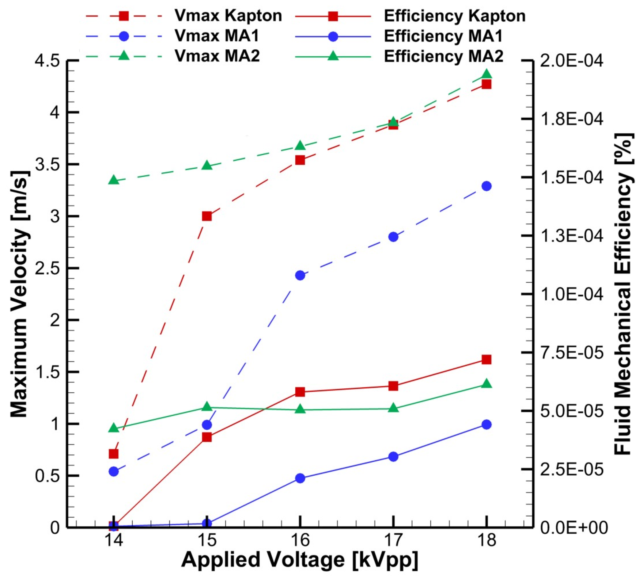
3.3. Plasma-Induced Flow Mechanical Characterization

Plasma-induced flow velocity measurements were performed in order to evaluate the ability of the different plasma actuators for flow control. Figure 5a–c show the velocity profiles obtained for the Kapton, MA1, and MA2 actuators, respectively, operating at various voltage levels and a frequency of 24 kHz. The final results presented in these figures were obtained by averaging 10 measurements, which allowed us to confer them with an uncertainty of less than 0.1 m/s.
As expected, the plasma-induced wall jet was measurable in the regions very close to the surface, at distances of up to 4 mm from the surface. The results demonstrate that the MA2 sample could reach higher velocities than the conventional Kapton actuator, mainly for lower applied voltages. However, the results also indicate that MA2 reaches a stagnation in the evolution of the velocities with the applied voltage faster than the Kapton actuator. Regarding the MA1 sample, we verified that it allows us to induce wall jet velocities of up to 3.5 m/s, which, although they might be enough to perform flow control in several applications, are somewhat lower than the wall jet velocity provided by Kapton and MA2 operating at the same applied voltage. Therefore, we may conclude that, despite higher material porosity leading to a decrease in the actuator’s power consumption, it also reduces the kinetic power transferred by the actuator to the adjacent air.
For a complete understanding of the performance of alumina ceramics as dielectric barriers in plasma actuators, the fluid mechanical power of the device was estimated. The fluid mechanical power describes the part of the power transferred by the actuator to induce the plasma wall jet and is calculated by considering that it corresponds to the balance of the kinetic energy density flow rate. Therefore, it can be expressed according to the following equation:
P m = 0 1 2 ρ u ( y ) 3 l d y
where ρ is the fluid density, in this case, air, u(y) is the velocity along the height, and l is the plasma spanwise length. After the quantification of the fluid mechanical power, the fluid mechanical efficiency was estimated, as described in Equation (4), and was considered a performance evaluation parameter.
η m = P m P ¯ × 100 %
Figure 6 exposes the results obtained for the maximum induced flow velocity and fluid mechanical efficiency. As we can observe, the fluid mechanical efficiency is very low for any of the tested actuators because the fluid mechanical power is very small, in the order of just a few milliwatts, comparatively to the average power consumed by each actuator. Nevertheless, these results are consistent with the values reported in the literature [28]. The observed phenomenon happens because, in fact, most of the power applied to the actuator is dissipated as dielectric and gas heating while the other part is lost as reactive power and power expended to maintain the discharge plasma [20].
From the analysis of Figure 6, we conclude that the MA2 actuator effectively allowed us to induce higher wall jet velocities than the Kapton and MA1 actuators. For lower applied voltage levels of up to 14 kVpp and 15 kVpp, the velocity of the wall jet induced by the MA2 plasma actuator is larger than the velocity induced by the Kapton actuator and, besides that, the power consumption of MA2 is lower than Kapton, which results in a considerably higher fluid mechanical efficiency. For higher voltage levels, MA2’s induced velocity starts to stagnate while Kapton’s induced flow velocity keeps increasing with the increase in the applied voltage level. Due to this, for applied voltages above 16 kVpp, the fluid mechanical efficiency of the Kapton actuator surpasses the MA2 actuator. Once again, we observed that the high porosity of the MA1 sample does not benefit the active flow control performance of the plasma actuator device since it resulted in lower plasma-induced flow velocity and lower fluid mechanical efficiency for any of the applied voltage levels. With these results, we can conclude that the produced alumina ceramics are a material with great potential for DBD plasma actuator fabrication, being able to produce higher fluid mechanical efficiencies than the conventional Kapton actuator. In addition, the tested alumina ceramics presented fewer signs of surface degradation, indicating higher durability than the Kapton actuator, which, at higher applied voltage levels, started to show discoloration and dielectric surface degradation in the region of the plasma streamers formation. However, future works must be carried out to present evidence of the potential higher durability of the tested ceramics.
Compared to Kapton actuators, one drawback of alumina ceramics relates to the rigidity of these dielectrics after being manufactured, which cannot be as flexible as Kapton. Nevertheless, by using 3D printing techniques, for instance, ceramic dielectrics can be produced with quite complex shapes depending on the desired application [47]. On the other hand, we must emphasize that the tested ceramics present additional features that are not accomplished by Kapton, they present high-temperature resistance characteristics and are also suitable for TBC (Thermal Barrier Coating) and TPS (Thermal Protection Systems) applications [32]. Therefore, ceramic dielectric barriers will be very important for plasma actuators’ high-temperature applications such as turbine blade film cooling enhancement [48,49] and plasma-assisted combustion [50,51]. This represents a great advantage over Kapton, which is a polymer and cannot operate under high temperatures and under ultra-violet exposure without being degraded and rupturing.
To conclude, the results also demonstrated that ceramic porosity has a strong influence on the plasma actuator fluid mechanical performance, and by manipulating the porosity of the material during the fabrication process, the fluid mechanical efficiency might increase. The influence of the dielectric material porosity on surface plasma actuators has not been studied yet, and there is a lack of information in the literature on this topic. However, previous works carried out by Ran J. et al. [52,53] have demonstrated that the morphology of the dielectric materials greatly affects the performance of the plasma device and plays a crucial role in the formation of the Atmospheric Pressure Townsend Discharge in the open air. Although the works of Ran J. et al. [52,53] focused on the roughness effect, porosity is also a crucial parameter in the dielectric’s morphology. In their work, the authors explained that once the number of free charges drops or the electric field weakens, the phenomenon ceases. When we have a material with higher porosity, the pores will create local deflections of the electric field lines, due to the medium change, which, in turn, will weaken the electric field generated. This will lead to a weaker discharge formation, which explains the lower power consumption and lower plasma-induced flow velocity effect observed for the material with higher porosity (MA1 in comparison with MA2).

4. Conclusions

The dielectric material layer plays a highly important role in a plasma actuator’s performance and lifetime. Considering the drawbacks of polymeric materials pointed out in the literature, in the current work, alumina-based ceramics were proposed and studied as dielectric barrier discharge of a surface plasma actuator device. Two different samples were fabricated with the same composition and different porosities and tested as plasma actuator devices.
From the microstructural analysis, it was clear that MA1 presented a higher content of porosity, interconnectivity between pores, fewer points of contact among grains, and higher microstructure heterogeneity, while MA2 showed a greater compaction degree and higher densification of the material, resulting in an apparent porosity of 34.6% and 7.0% for MA1 and MA2, respectively.
After that, the alumina ceramic plates were tested as dielectric barriers for plasma actuator applications and the power consumption was estimated by applying the electrical current method and electrical charge method. We concluded that both alumina-based actuators presented lower power consumption than the conventional Kapton actuator for applied voltages of up to 17 kVpp. Furthermore, by comparing the values obtained for the MA1 and MA2 samples, we highlighted that a decrease in the ceramic plate porosity leads to an increase in power consumption. The electrical charge method was also applied in order to analyze the voltage–charge cyclograms and corroborate the power consumption results. However, from the capacitance measurements, we verified that the Kapton actuator presented higher capacitance than the alumina-based ceramics, which was not expected since the dielectric permittivity of Kapton is lower than alumina. The main reason for this lies in the sintering process used, which did not allow us to accurately control the thickness of the alumina ceramics produced. We verified that the ceramic plates produced do not present a fully constant thickness and, thus, we concluded that the actuator electrodes were positioned in a region where the thickness of the dielectric is slightly greater than 5 mm. This explains the smaller capacitance of the alumina-based ceramic actuators in comparison to the Kapton actuator.
To finalize, plasma-induced flow velocity measurements were conducted, and the flow control performance of the various plasma actuators was evaluated. The results demonstrated that the MA2 sample could reach higher velocities than the conventional Kapton actuator, mainly for lower applied voltages. For applied voltage levels of up to 14 kVpp and 15 kVpp, the velocity of the wall jet induced by the MA2 plasma actuator was larger than the velocity induced by the Kapton actuator and, in addition, the power consumption of MA2 was lower than Kapton, which resulted in a considerable higher fluid mechanical efficiency. For higher voltage levels, the MA2’s induced velocity started to stagnate while the Kapton’s induced flow velocity kept increasing with the increase in the applied voltage level. Due to that, for applied voltages above 16 kVpp, the fluid mechanical efficiency of the Kapton actuator surpasses the MA2 actuator. In addition, we showed that the high porosity of the MA1 sample does not benefit the active flow control performance of the plasma actuator device since it resulted in lower plasma-induced flow velocity and lower fluid mechanical efficiency. Overall, we concluded that the alumina ceramics produced are materials with great potential for DBD plasma actuator fabrication, with the ability to provide higher fluid mechanical efficiencies than the conventional Kapton actuator with fewer signs of surface degradation, which indicates higher durability and an extended lifetime. Moreover, the ceramics dielectrics studied presented high-temperature resistance characteristics, which are also suitable for TBC (Thermal Barrier Coating) and TPS (Thermal Protection Systems) applications, when compared to Kapton.

Author Contributions

Conceptualization, F.F.R. and K.O.S.; methodology, F.F.R., K.O.S., J.N.-P., J.C.P. and A.P.S.; formal analysis, F.F.R. and K.O.S.; investigation, F.F.R., K.O.S. and J.N.-P.; resources, J.C.P. and A.P.S.; data curation, F.F.R. and K.O.S.; writing—original draft preparation, F.F.R. and K.O.S.; writing—review and editing, F.F.R., K.O.S., J.N.-P., J.C.P. and A.P.S.; supervision, J.C.P. and A.P.S.; project administration, F.F.R., J.C.P. and A.P.S.; funding acquisition, J.C.P. and A.P.S. All authors have read and agreed to the published version of the manuscript.

Funding

This research was funded by the Portuguese Foundation for Science and Technology, I.P. (FCT, I.P.) through the research unit C-MAST (Center for Mechanical and Aerospace Science and Technology), Research Unit No. 151, project grant number UIDB/00151/2020 (https://doi.org/10.54499/UIDB/00151/2020) and grant number UIDP/00151/2020 (https://doi.org/10.54499/UIDP/00151/2020), and through the contract of João Nunes-Pereira within the framework of the FCT Stimulus of Scientific Employment, Individual Support: 2022.05613.CEECIND (https://doi.org/10.54499/2022.05613.CEECIND/CP1746/CT0001).

Data Availability Statement

Data are contained within the article.

Conflicts of Interest

The authors declare no conflicts of interest.

References

  1. Clyde Warsop, Active Flow Control Using MEMS. In MEMS Aerospace Applications, RTO/NATO. Available online: https://apps.dtic.mil/sti/citations/tr/ADA425494 (accessed on 1 February 2004).
  2. Wang, J.; Feng, L. Introduction. In Flow Control Techniques and Applications; Cambridge University Press (CUP): Cambridge, UK, 2018; pp. 1–22. ISBN 9781107161566. [Google Scholar]
  3. Batikh, A.; Baldas, L.; Colin, S. Application of Active Flow Control on Aircrafts—State of the Art. 2017. Available online: https://hal.science/hal-01820331 (accessed on 20 September 2023).
  4. Bouremel, Y.; Li, J.; Zhao, Z.; Debiasi, M. Effects of AC Dielectric Barrier Discharge Plasma Actuator Location on Flow Separation and Airfoil Performance. Procedia Eng. 2013, 67, 270–278. [Google Scholar] [CrossRef]
  5. Viguera, R.; Anzai, Y.; Sasaki, Y.; Nonomura, T. Experimental Observations of Transient Flows in Separation Control Using a Plasma Actuator. Actuators 2023, 12, 218. [Google Scholar] [CrossRef]
  6. Zhang, X.; Huang, Y.; Wang, X.; Wang, W.; Tang, K.; Li, H. Turbulent boundary layer separation control using plasma actuator at Reynolds number 2000000. Chin. J. Aeronaut. 2016, 29, 1237–1246. [Google Scholar] [CrossRef]
  7. Visbal, M.R.; Gaitonde, D.V.; Roy, S. Control of transitional and turbulent flows using plasma-based actuators, Collection of Technical Papers. In Proceedings of the 36th AIAA Fluid Dynamics Conference and Exhibit, San Francisco, CA, USA, 5–8 June 2006; Volume 2, pp. 1087–1108. [Google Scholar] [CrossRef]
  8. Al-Sadawi, L.; Chong, T.P.; Kim, J.H. Aero-dynamic noise reduction by plasma actuators for a flat plate with blunt trailing edge. J. Sound Vib. 2019, 439, 173–193. [Google Scholar] [CrossRef]
  9. Chen, Z.; Wen, C.-Y. Flow control of a D-shaped bluff body using different DBD plasma actuators. J. Fluids Struct. 2021, 103, 103292. [Google Scholar] [CrossRef]
  10. Konstantinidis, E. Active Control of Bluff-Body Flows Using Plasma Actuators. Actuators 2019, 8, 66. [Google Scholar] [CrossRef]
  11. Grundmann, S.; Tropea, C. Experimental transition delay using glow-discharge plasma actuators. Exp. Fluids 2007, 42, 653–657. [Google Scholar] [CrossRef]
  12. Grundmann, S.; Tropea, C. Active cancellation of artificially introduced Tollmien–Schlichting waves using plasma actuators. Exp. Fluids 2007, 44, 795–806. [Google Scholar] [CrossRef]
  13. Grundmann, S.; Tropea, C. Experimental damping of boundary-layer oscillations using DBD plasma actuators. Int. J. Heat Fluid Flow 2009, 30, 394–402. [Google Scholar] [CrossRef]
  14. Kim, D.; Do, H.; Choi, H. Drag reduction on a three-dimensional model vehicle using a wire-to-plate DBD plasma actuator. Exp. Fluids 2020, 61, 135. [Google Scholar] [CrossRef]
  15. Wang, C.-C.; Wen, C.-P. Aerodynamic drag reduction for a truck model using DBD plasma actuators. Adv. Mech. Eng. 2022, 14, 16878132221087852. [Google Scholar] [CrossRef]
  16. Liu, Y.; Kolbakir, C.; Hu, H.; Hu, H. A comparison study on the thermal effects in DBD plasma actuation and electrical heating for aircraft icing mitigation. Int. J. Heat Mass Transf. 2018, 124, 319–330. [Google Scholar] [CrossRef]
  17. Li, C.; Hu, H.; Meng, X.; Cai, J.; Hu, H. Aerodynamic and Thermal Effects of Plasma Actuators on Anti-icing over an Airfoil. Lect. Notes Electr. Eng. 2019, 459, 1008–1019. [Google Scholar] [CrossRef]
  18. Meng, X.; Hu, H.; Li, C.; Abbasi, A.A.; Cai, J.; Hu, H. Mechanism study of coupled aerodynamic and thermal ef-fects using plasma actuation for anti-icing. Phys. Fluids 2019, 31, 37103. [Google Scholar] [CrossRef]
  19. Kaneko, Y.; Nishida, H.; Tagawa, Y. Visualization of the Electrohydrodynamic and Thermal Effects of AC-DBD Plasma Actuators of Plate- and Wire-Exposed Electrodes. Actuators 2022, 11, 38. [Google Scholar] [CrossRef]
  20. Rodrigues, F.; Abdollahzadehsangroudi, M.; Nunes-Pereira, J.; Páscoa, J. Recent Developments on Dielectric Barrier Discharge (DBD) Plasma Actuators for Icing Mitigation. Actuators 2023, 12, 5. [Google Scholar] [CrossRef]
  21. Xie, L.; Liang, H.; Zong, H.; Liu, X.; Li, Y. Multipurpose distributed dielectric-barrier-discharge plasma actua-tion: Icing sensing, anti-icing, and flow control in one. Phys. Fluids 2022, 34, 071701. [Google Scholar] [CrossRef]
  22. Thomas, F.O.; Corke, T.C.; Iqbal, M.; Kozlov, A.; Schatzman, D. Optimization of Dielectric Barrier Discharge Plasma Actuators for Active Aerodynamic Flow Control. AIAA J. 2009, 47, 2169–2178. [Google Scholar] [CrossRef]
  23. Hink, R.; Pipa, A.V.; Schäfer, J.; Caspari, R.; Weichwald, R.; Foest, R.; Brandenburg, R. Influence of dielectric thickness and electrode structure on the ion wind generation by micro fabricated plasma actuators. J. Phys. D Appl. Phys. 2020, 53, 405201. [Google Scholar] [CrossRef]
  24. Benard, N.; Moreau, E. Electrical and mechanical characteristics of surface AC dielectric barrier discharge plasma actuators applied to airflow control. Exp. Fluids 2014, 55, 1846. [Google Scholar] [CrossRef]
  25. Rigit, A.R.H.; La, K.C.; Bong, D.B.L. Degradation of a dielectric barrier discharge plasma actuator. In Proceedings of the IEEE International Conference on Properties and Applications of Dielectric Materials, Harbin, China, 19–23 July 2009; pp. 569–572. [Google Scholar] [CrossRef]
  26. Hanson, R.E.; Houser, N.M.; Lavoie, P. Dielectric material degradation monitoring of dielectric barrier dis-charge plasma actuators. J. Appl. Phys. 2014, 115, 43301. [Google Scholar] [CrossRef]
  27. Pons, J.; Oukacine, L.; Moreau, E.; Tatibouet, J.-M. Observation of Dielectric Degradation After Surface Dielectric Barrier Discharge Operation in Air at Atmospheric Pressure. IEEE Trans. Plasma Sci. 2008, 36, 1342–1343. [Google Scholar] [CrossRef]
  28. Rodrigues, F.F.; Pascoa, J.C.; Trancossi, M. Experimental Analysis of Alternative Dielectric Materials for DBD Plasma Actuators. In Proceedings of the ASME International Mechanical Engineering Congress and Exposition, Pittsburgh, PA, USA, 9–15 November 2018. [Google Scholar]
  29. Rodrigues, F.F.; Pereira, J.N.; Abdollahzadeh, M.; Pascoa, J.; Mendez, S.L. Comparative Evaluation of Dielectric Materials for Plasma Actuators Active Flow Control and Heat Transfer Applications. In Proceedings of the ASME 2021 Fluids Engineering Division Summer Meeting, Virtual, 10–12 August 2021. [Google Scholar] [CrossRef]
  30. Nunes-Pereira, J.; Rodrigues, F.F.; Abdollahzadehsangroudi, M.; Páscoa, J.C.; Lanceros-Mendez, S. Improved performance of polyimide Cirlex-based dielectric barrier discharge plasma actuators for flow control. Polym. Adv. Technol. 2021, 33, 1278–1290. [Google Scholar] [CrossRef]
  31. Shvydyuk, K.O.; Rodrigues, F.F.; Nunes-Pereira, J.; Páscoa, J.C.; Lanceros-Mendez, S.; Silva, A.P. Long-lasting ceramic composites for surface dielectric barrier discharge plasma actuators. J. Eur. Ceram. Soc. 2023, 43, 6112–6121. [Google Scholar] [CrossRef]
  32. Shvydyuk, K.O.; Nunes-Pereira, J.; Rodrigues, F.F.; Silva, A.P. Review of Ceramic Composites in Aeronautics and Aerospace: A Multifunctional Approach for TPS, TBC and DBD Applications. Ceramics 2023, 6, 195–230. [Google Scholar] [CrossRef]
  33. C20 Standard Test Methods for Apparent Porosity, Water Absorption, Apparent Specific Gravity, and Bulk Density of Burned Refractory Brick and Shapes by Boiling Water. Available online: https://www.astm.org/c0020-00r22.html (accessed on 20 September 2023).
  34. Ashpis, D.E.; Laun, M.C.; Griebeler, E.L.; Zheng, B.; Ke, X.; Ge, C.; Zhu, Y.; Wu, Y.; Liu, F.; Luo, S.; et al. Progress Toward Accurate Measurement of Dielectric Barrier Discharge Plasma Actuator Power. AIAA J. 2017, 55, 2254–2268. [Google Scholar] [CrossRef] [PubMed]
  35. Kriegseis, J.; Grundmann, S.; Tropea, C. Power consumption, discharge capacitance and light emission as measures for thrust production of dielectric barrier discharge plasma actuators. J. Appl. Phys. 2011, 110, 013305. [Google Scholar] [CrossRef]
  36. Pons, J.; Moreau, E.; Touchard, G. Asymmetric surface dielectric barrier discharge in air at atmospheric pressure: Electrical properties and induced airflow characteristics. J. Phys. D Appl. Phys. 2005, 38, 3635–3642. [Google Scholar] [CrossRef]
  37. Rodrigues, F.F.; Pascoa, J.C. Implementation of Stair-Shaped Dielectric Layers in Micro- and Macroplasma Actuators for Increased Efficiency and Lifetime. J. Fluids Eng. 2020, 142, 104502. [Google Scholar] [CrossRef]
  38. Somton, K.; Dateraksa, K.; Laoratanakul, P.; McCuiston, R. Shrinkage and properties of die pressed alumina produced from different granule sources. AIP Conf. Proc. 2020, 2279, 060003. [Google Scholar] [CrossRef]
  39. Pribyl, R.; Stastny, P.; Pazderka, M.; Kelar, J.; Tucekova, Z.K.; Zemanek, M.; Trunec, M.; Cernak, M. Properties of MgAl2O4 doped alumina barrier layers for dielectric barrier discharge. J. Phys. D Appl. Phys. 2020, 53, 505202. [Google Scholar] [CrossRef]
  40. Lindner, M.; Pipa, A.V.; Brandenburg, R.; Schreiner, R. Expansion of surface barrier discharge scrutinized. Plasma Sources Sci. Technol. 2022, 31, 105018. [Google Scholar] [CrossRef]
  41. Synek, P.; Zemánek, M.; Kudrle, V.; Hoder, T. Advanced electrical current measurements of microdischarges: Evidence of sub-critical pulses and ion currents in barrier discharge in air. Plasma Sources Sci. Technol. 2018, 27, 045008. [Google Scholar] [CrossRef]
  42. Synek, P.; Akishev, Y.S.; Petryakov, A.; Trushkin, N.; Vorac, J.; Hoder, T. Electrical analysis and ultra-fast sequential imaging of surface barrier discharge with streamer-leader sequence generated with 100 kHz frequency at the water interface. Plasma Sources Sci. Technol. 2019, 28, 095018. [Google Scholar] [CrossRef]
  43. Roth, J.R.; Dai, X.; Rahel, J.; Shermann, D.M. The physics and phenomenology of paraelectric One Atmosphere Uniform Glow Discharge Plasma (OAUGDPTM) actuators for aerodynamic flow control. In Proceedings of the 43rd AIAA Aerospace Sciences Meeting and Exhibit-Meeting Papers, Reno, NV, USA, 10–13 January 2005; pp. 14057–14068. [Google Scholar] [CrossRef]
  44. Wilde, N.D.; Xu, H.; Gomez-Vega, N.; Barrett, S.R.H. A model of surface dielectric barrier discharge power. Appl. Phys. Lett. 2021, 118, 154102. [Google Scholar] [CrossRef]
  45. Birey, H. Thickness dependence of the dielectric constant and resistance of Al2O3 films. J. Appl. Phys. 1977, 48, 5209–5212. [Google Scholar] [CrossRef]
  46. Wang, X.; Engel, J.; Liu, C. Liquid crystal polymer (LCP) for MEMS: Processes and applications. J. Micromech. Microeng. 2003, 13, 628–633. [Google Scholar] [CrossRef]
  47. Chen, Z.; Li, Z.; Li, J.; Liu, C.; Lao, C.; Fu, Y.; Liu, C.; Li, Y.; Wang, P.; He, Y. 3D printing of ceramics: A review. J. Eur. Ceram. Soc. 2018, 39, 661–687. [Google Scholar] [CrossRef]
  48. Audier, P.; Fénot, M.; Bénard, N.; Moreau, E. Film cooling effectiveness enhancement using surface dielectric barrier discharge plasma actuator. Int. J. Heat Fluid Flow 2016, 62, 247–257. [Google Scholar] [CrossRef]
  49. Li, G.; Wang, Q.; Huang, Y.; Zhang, H. Large eddy simulation of film cooling effectiveness on a turbine vane pressure side with a saw-tooth plasma actuator. Aerosp. Sci. Technol. 2021, 112, 106615. [Google Scholar] [CrossRef]
  50. Liu, P.; He, L.; Zhao, B. Discharge and Optical Emission Spectrum Characteristics of a Coaxial Dielectric Barrier Discharge Plasma-Assisted Combustion Actuator. J. Spectrosc. 2020, 2020, 6034848. [Google Scholar] [CrossRef]
  51. Khasare, S.; Bagherighajari, F.; Dolati, F.; Mahmoudimehr, J.; Páscoa, J.; Abdollahzadehsangroudi, M. The effect of the dielectric barrier discharge plasma actuator in the control of non-reactive flow in a non-premixed bluff body burner. Phys. Fluids 2023, 35, 075135. [Google Scholar] [CrossRef]
  52. Ran, J.; Zhang, X.; Ge, D.; Li, X.; Li, X. Effect of Dielectric Surface Morphology on Dielectric Barrier Discharge Mode in Air at Atmospheric Pressure. IEEE Trans. Plasma Sci. 2020, 49, 214–218. [Google Scholar] [CrossRef]
  53. Ran, J.; Li, C.; Ma, D.; Luo, H.; Li, X. Homogeneous dielectric barrier discharges in atmospheric air and its influencing factor. Phys. Plasmas 2018, 25, 033511. [Google Scholar] [CrossRef]
Figure 1. Schematic of the experimental tests; (a) fabricated ceramics-based plasma actuator with the respective geometrical definition for Pitot tube plasma-induced flow velocity measurements; (b) plasma discharge visualization for the Kapton actuator operating at an applied voltage of 18 kVpp and a frequency of 24 kHz.
Ceramics 07 00012 g001
Figure 2. SEM images obtained for the fabricated alumina ceramic samples: (a) MA1 at magnification factor of 5000×, (b) MA2 at magnification factor of 5000×, (c) MA1 at magnification factor of 10,000× and (d) MA2 at magnification factor of 10,000×.
Ceramics 07 00012 g002aCeramics 07 00012 g002b
Figure 3. Electric current method analysis for the various plasma actuators operating at a frequency of 24 kHz: (a) voltage and current waveforms at 15 kVpp and (b) power consumption estimation for different applied voltages.
Ceramics 07 00012 g003
Figure 4. Electrical charge method analysis: (a) charge–voltage curves at 10 kVpp, (b) charge–voltage curves at 15 kVpp, and (c) power consumption estimation for different applied voltages (24 kHz).
Ceramics 07 00012 g004
Figure 5. Velocity profiles obtained for the various actuators operating at different voltage levels and the same frequency (24 kHz): (a) Kapton, (b) MA1, and (c) MA2.
Ceramics 07 00012 g005
Figure 6. Maximum plasma-induced flow velocity and fluid mechanical efficiency obtained for the various plasma actuators operating at different voltage levels and the same frequency (24 kHz).
Ceramics 07 00012 g006
Disclaimer/Publisher’s Note: The statements, opinions and data contained in all publications are solely those of the individual author(s) and contributor(s) and not of MDPI and/or the editor(s). MDPI and/or the editor(s) disclaim responsibility for any injury to people or property resulting from any ideas, methods, instructions or products referred to in the content.

