Abstract
Turbine systems equipped with doubly fed induction generation (DFIG) are becoming increasingly vital in wind power generation, with the reliability of the devices serving as a pillar in the industrial sector. Thermal stress and lifetime assessment are fundamental indicators in this regard. This paper primarily addresses the thermal stress and lifespan of power semiconductor devices utilized in a DFIG grid-side converter (GSC) and rotor-side converter (RSC). PLECS (Piecewise Linear Electrical Circuit Simulation) is employed to validate the electrical and thermal stress of the power devices. Additionally, Ansys Icepak, a finite element analysis (FEA) software, is utilized to confirm temperature fluctuations under various operations. The power consumption and junction temperature of the power devices in the GSC and RSC of a 2 MW DFIG are compared. It is evident that the most stressed power semiconductor is the IGBT for the GSC with a temperature swing of 3.4 °C, while the diode in the RSC is the most stressed with a temperature swing of 10.1 °C. This paper also presents a lifetime model to estimate the lifespan of the power device based on the annual wind profile. By considering the annual mission profile, we observe that the lifetime of the back-to-back power converter is limited by the diode of the RSC, whose B10 lifetime is calculated at 15 years.
1. Introduction
The 2024 Global Offshore Wind Report marks a new frontier in the worldwide growth of offshore wind. The global offshore market is expected to grow from 10.8 GW in 2023 to 37.1 GW in 2028, bringing its share of new global installations from today’s 9% to 20% by 2028 [1]. It has been demonstrated that wind turbine generation has played a very important role and will continue to do so in the coming decade.
DFIG is the primary choice of wind turbine manufacturers because it is an extremely cost-effective solution. The reliable operation of the converter module and the lifetime cycle of the power converter and power semiconductor devices have become important factors restricting DFIG [2,3].
The capacity of the back-to-back power converter is relatively small compared to the DFIG, leading to its cost-effectiveness from the viewpoint of economics. The rotor in DFIG is linked to the power grid using the RSC and the GSC, while the stator side is directly connected to the grid. The function of the GSC is to keep the DC bus voltage fixed and meet the reactive power demand according to the grid codes, while the RSC can produce active power to the power grid through following maximum power point tracking (MPPT) and providing the exciting current for DFIG [4].
DFIG is typically controlled through coordinate transformation, which gives the possibility to control its active and reactive power independently. The vector control is commonly used, including the stator voltage orientation and stator flux orientation [5,6,7,8]. If the stator voltage orientation is applied, the synchronous rotating frame is aligned with the stator voltage.
In order to obtain a device’s lifetime model, the power cycling testing of wind turbine power devices is required under different stress conditions [9,10,11]. Common power cy-cling methods can be classified into active power cycles (self-operation) and passive power cycles (external thermal chamber) [12,13]. In respect to active power cycling, it can be further divided into DC power cycling and AC power cycling according to the current passing through. Active power cycling has been studied more because of its flexible control and diverse temperature monitoring methods [14,15,16,17,18]. At the same time, according to the control parameters of each cycle, it is divided into constant current, constant power, and constant junction temperature fluctuation. Constant current indicates that the current applied to the IGBT remains constant. The power loss level of the IGBT device is maintained at a fixed value for the constant power approach. In the case of constant junction temperature fluctuation, the power cycle to failure lifetime of the device is controlled by junction temperature fluctuations [19]. In this process, the physical mechanism of fatigue failure (crack expansion rate, degradation growth in the solder joint, bond wire lift-off, electrical migration and aluminum metal reconfiguration) can be studied [20,21]. The remaining part of the power cycle test focuses on the accuracy of the lifetime assessment by selecting thermally sensitive parameters (such as on-state voltage drop, maximum temperature and junction temperature fluctuation) [14,20].
The key to investigating the reliability of the DFIG power converter is to understand its failure mechanisms, where thermal-mechanical stress-related degradation is dominant for power semiconductors. Due to the different features and complex control strategies of the back-to-back power converter, the simulation is needed to efficiently evaluate the loading conditions and obtain the equivalent thermal stress of the wind power converter. Therefore, it is necessary to establish the theoretical models and to compare the thermal stress of the power semiconductor devices, which forms the basis for subsequent simulation. Prior-art DFIG research mainly focuses on the fields of converter control and fault ride-through. There are few studies on the thermal stress and lifetime of turbine generator devices in sub-synchronous and super-synchronous states. This study aims to provide guidelines for power semiconductor reliability pre-design and lifetime extension.
The remaining part of this paper is organized as follows. Section 2 describes the topology and operating principle of the DFIG systems, where the case conditions are introduced. GSC and RSC models as well as their control principles are presented in Section 3. The power loss model and thermal model are described in Section 4. Section 5 presents a thermal stress comparison between the DFIG GSC and RSC, including theoretical calculations and simulation verification. In Section 6, the finite element simulations of the two power converters are compared. Section 7 estimates the lifespan of the power semiconductor based on the annual mission profile. Finally, some concluding remarks are drawn in Section 8.
2. Operation Principle of DFIG
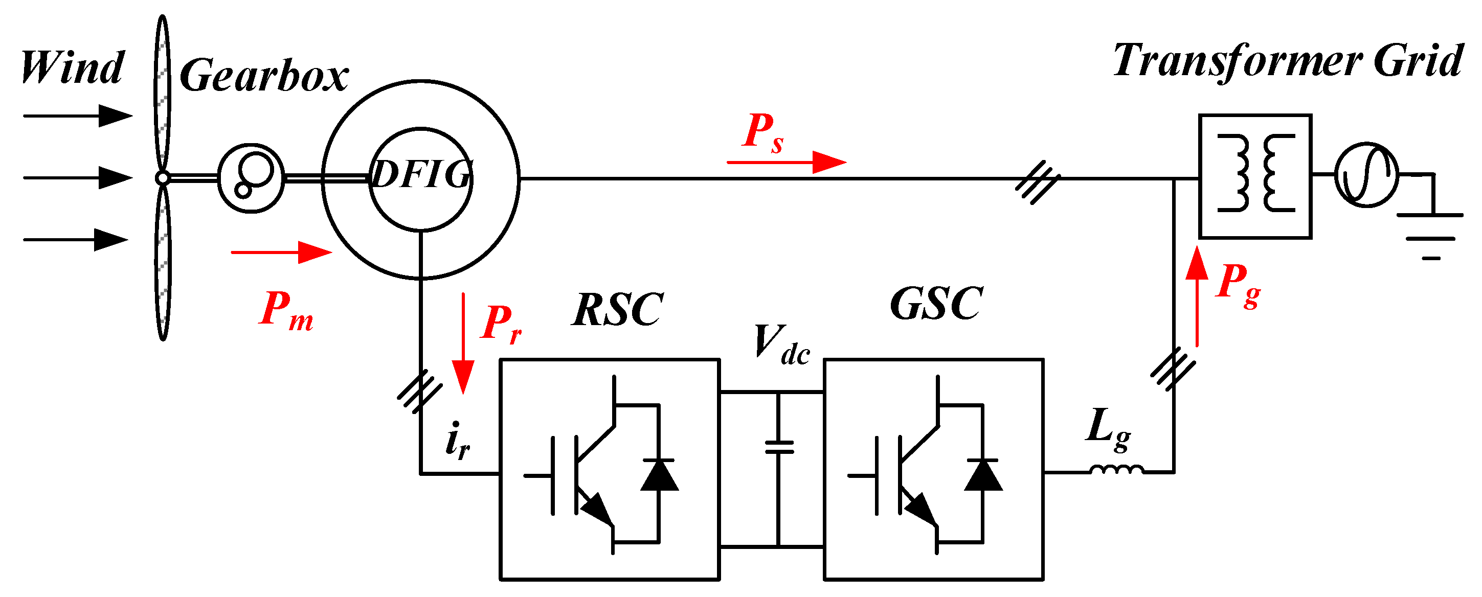
As shown in Figure 1, a typical DFIG system consists of a generator, gearbox, transformer, power grid, a cascaded three-phase power converter (back-to-back power converter), a dc-link capacitor bank, and a filter inductor [22]. The wind power captured using the DFIG turbine is converted into electrical energy via the generator and transmitted to the grid through the stator and rotor windings. The main advantage of DFIG is that it maintains the amplitude and frequency of the output voltage at a constant value regardless of the wind turbine rotor speed. Therefore, the DFIG can be connected directly to the AC power grid and always remain synchronized. In this process, the structure and independent control of GSC and RSC played a crucial role. Since the power converter of the wind turbine only needs to handle a small part of the rated power, the converter power devices have higher lifetime cycles under different thermal profiles. Based on the rotor speed, DFIG operates in either a super-synchronous state (when the slip becomes negative) or a sub-synchronous state (when the slip becomes positive). In order to simplify the analysis, the mechanical losses inside the generator are ignored. Therefore, Pm is the mechanical power of DFIG, Pe is the input air-gap electromagnetic power and Pe ≈ Pm. Considering ‘s’ as the slip of the rotor, the relation between slip and the rotating speed is expressed as s = (nr − ne)/nr, where nr and ne are the rotor speed and rated synchronous speed of the DFIG, respectively. The stator active power Ps and rotor active power Pr compose the mechanical power Pm. Therefore, the power injected into the grid is Pg = (1 − s)Ps. Depending on the slip value, it generates or absorbs active power from the rotor side of the generator.
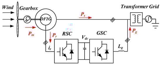
Figure 1.
DFIG topology with back-to-back power converter.
The active power curve based on wind speed is one of the methods to control the active power of the DFIG wind turbine. According to the aerodynamic model [23,24], the active power generated using the wind turbine is determined by the power coefficient.
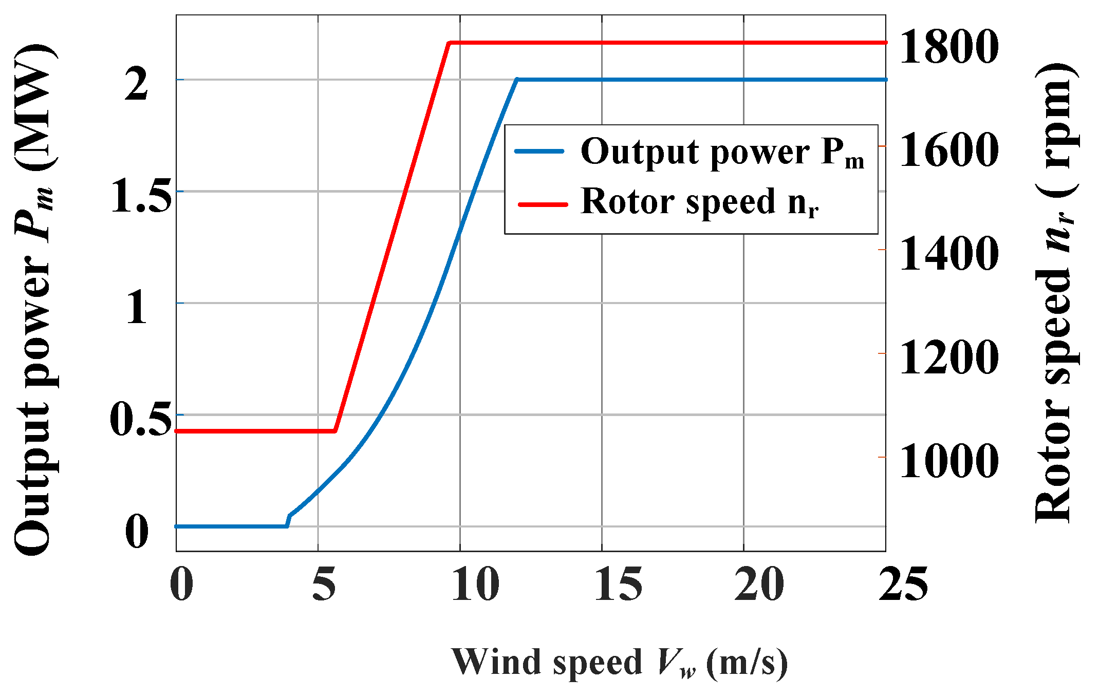
This case study applies a 2 MW wind turbine to investigate the thermal performance of converters and power semiconductors. The relationship between DFIG rotor speed and output power concerning the wind speed is shown in Figure 2. As the wind speed increases from the cut-in wind speed of 4 m/s to the rated wind speed of 12 m/s, the output power also increases to the rated value. The detailed parameters of the wind turbine system are listed in Table 1.
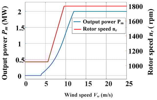
Figure 2.
DFIG output power and rotor speed at various wind speeds.

Table 1.
Parameters for wind turbine.
3. Model and Control of GSC and RSC
This paper takes the GSC and RSC as an example for analysis, where the grid voltage-oriented control approach is used with a dq reference rotating frame. As shown in Figure 3, the GSC control strategy includes two cascaded loops. The inner loop mainly focuses on the grid current ig, and the outer loop takes care of the reactive power Qg and dc-link voltage Udc. The d-axis grid current is used to keep the dc-link voltage constant, and the q-axis grid current regulates the reactive power [2,22].
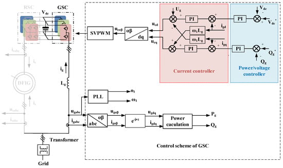
Figure 3.
Control scheme of the grid-side converter for the DFIG system.
If there is a single inductor in the GSC output side, the relationship under the rotating frame between the grid and GSC can be expressed as the following:
where ucg and ug denote the GSC converter output voltage and grid voltage, and Rg denotes the grid equivalent filter resistance. ig denotes the grid current. Lg denotes the filter inductance. ꞷ1 represents the stator angular frequency. The subscripts d and q are the variables under the d-axis and q-axis, respectively. The active power Pg and reactive power Qg flow between the GSC and grid will be proportional to igd and igq, respectively; the relationship can be expressed by
Based on (3), the active power is only related to the d-axis grid current. Meanwhile, under the unity power factor condition, the reactive power is zero, and the q-axis reference current is set to zero.
The objective of RSC is to regulate the stator active and reactive power injected into the power grid. As shown in Figure 4, the RSC control strategy also includes two cascaded control loops. The inner current loop ir regulates the d-axis and q-axis rotor current, and the outer loop decouples the reactive and active power of the stator side. Aligning the d-axis of the reference frame along the stator voltage vector position, the relationship between the rotor voltage and rotor current can be found:
where ur denotes the RSC rotor voltage. ir denotes the rotor current. Rr denotes the rotor resistance. Ls, Lr, and Lm denote the stator inductance, the rotor inductance, and the magnetizing inductance, respectively. σ represents the leakage coefficient and equals (LsLr − Lm2/LsLr). sl represents the slip of the induction generator and equals ꞷs/ꞷ1.
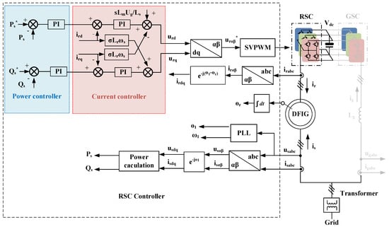
Figure 4.
Control scheme of the rotor-side converter for the DFIG system.
The stator’s active and reactive power flow can then be expressed by
where Ps and Qs denote the active and reactive power of the stator side. Us is the peak phase voltage of the stator. Due to the constant stator voltage, the stator side active power and reactive power are controlled via ird and irq, respectively.
4. Loss Model and Thermal Model
The power device dissipation of GSC and RSC mainly includes conduction loss and switching loss. Under specific wind speed conditions, the turbine will generate a specific frequency, voltage, current, and displacement angle in order to maintain maximum power point tracking. In the fundamental period, the linear approximation of the IGBT forward characteristics is assumed [22,24,25], and the GSC conduction loss PconT can be further simplified as follows:
where VCE0 means the collector-emitter initial voltage drop, and φ is the displacement angle of the output phase current and voltage. M denotes the voltage modulation index. Il denotes the peak value of the output current. For the conduction power loss of the RSC and GSC, the RSC current Il in (9) becomes half of the GSC, as the two paralleled power modules are selected for the RSC due to its higher current stress.
The MATLAB polynomial fitting method is used to represent the switching loss of the IGBT according to the turn-on loss and turn-off loss, respectively. In the fundamental period, the sum of turn-on loss and turn-off loss consists of the switching loss. The GSC switching loss PswT in a fundamental period can be calculated as follows:
where fsw is switching frequency. Vdc and denote dc-link voltage and reference dc-link voltage, respectively. aT, bT, and cT denote the corresponding coefficient of the fitting function, respectively. The above three parameters are obtained at the worst junction temperature (150 °C) from the datasheet. The diode switching loss only includes the reserve-recovery loss. It is worth noting that, the RSC current is also half of the GSC.
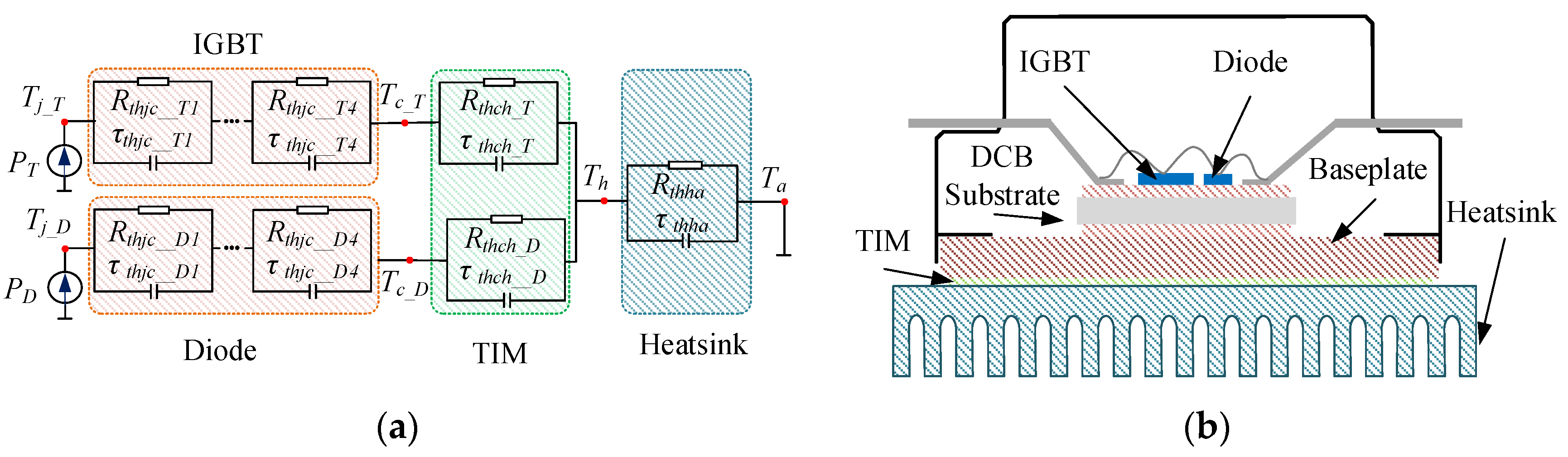
The thermal network of the power module is shown in Figure 5a. In general, in order to facilitate calculation, the junction-to-case RC network will be converted into a fourth-order Foster model (from junction to case) [26]. Combined with the thermal network mathematical model, as shown in Figure 5b, the actual physical material layers from top to bottom are the silicon chip, solder, direct copper bonding (DCB) substrate, the baseplate, thermal interface material (TIM), and the heatsink.
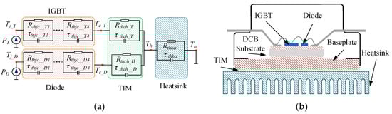
Figure 5.
Thermal model of IGBT power semiconductor module. (a) RC thermal network. (b) Basic layout of the power module.
According to the thermal profile in the condition of periodical power dissipation at steady state, the relationship of the mean junction temperature Tj_T and junction temperature swing ΔTj_T can be obtained as follows:
where Tj_T stands for the chip surface temperature, Tc_T indicates the case temperature, Th denotes heatsink temperature, Ta means ambient temperature, PT denotes total IGBT power loss, PD denotes total diode power loss, Rthjc_T, Rthha, and Rthjc_T are the junction-case, case-heatsink, and heatsink-ambient thermal resistance. Moreover, ton denotes half of the fundamental period and T is the fundamental period of the load current. τ denotes the thermal time constant of each network.
5. Power Devices Thermal Stress Comparison between DFIG GSC and RSC
In this section, the simulated loss dissipation and thermal cycling of the power device will be presented and compared with mathematical calculations from the loss and thermal models. A case study of the 2 MW DFIG system is carried out. The important parameters of the wind turbine are listed in Table 2, where the number of pole pairs p = 2. Moreover, the Danfoss P3 power module is selected [27].
Table 2.
Parameters and conditions of the DFIG GSC and RSC systems.
5.1. GSC and RSC Power Loss and Thermal Stress
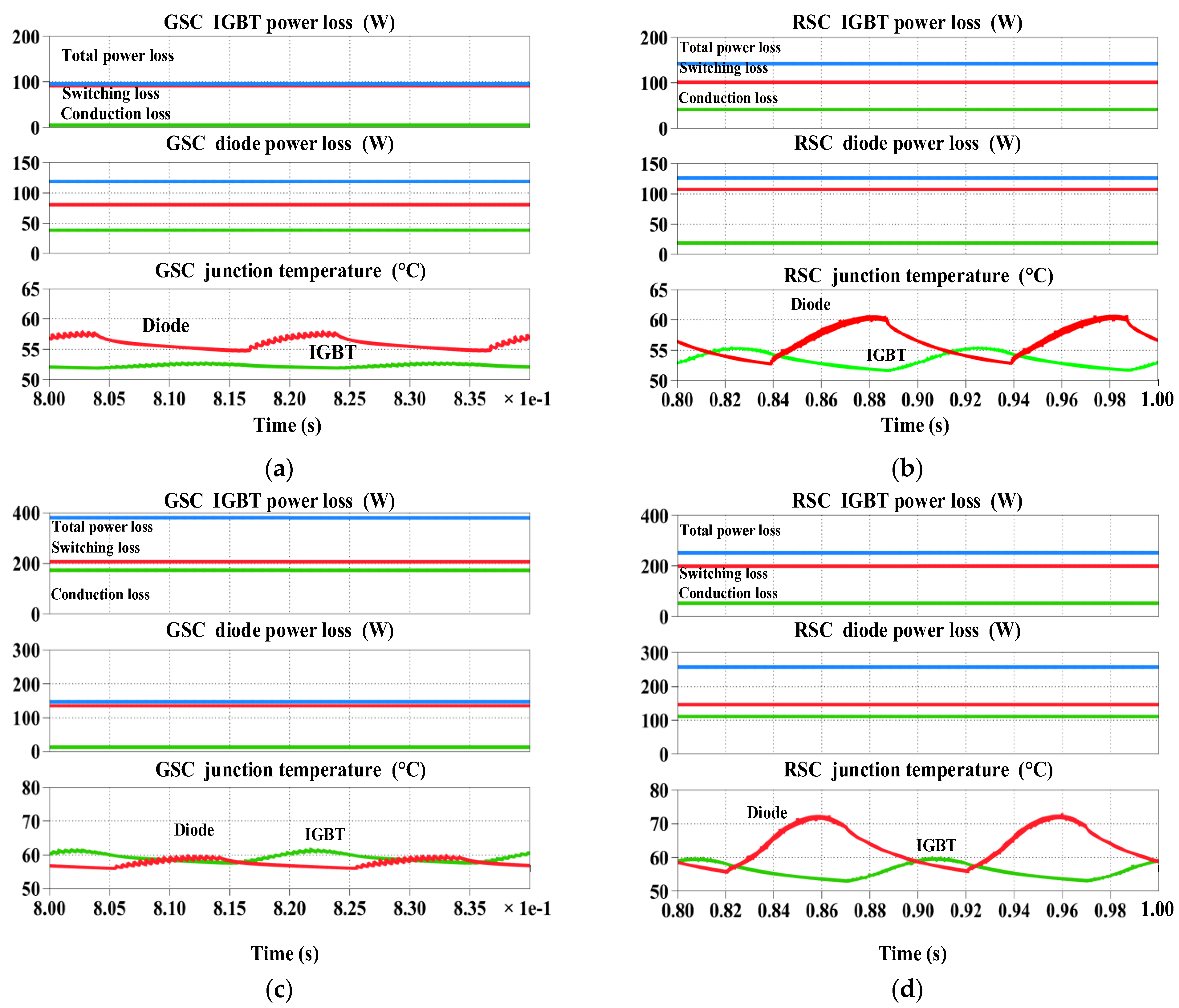
With the different wind speed conditions, there are different loading conditions for the GSC and RSC power semiconductor energy output and thermal stress. The sub-synchronous state (Vw = 6.8 m/s, Pm = 0.4 MW, nr = 1200 rpm, s = 0.2) and super-synchronous state (Vw = 12 m/s, Pm = 2 MW, nr = 1800 rpm, s = −0.2) are selected for working status comparison. Figure 6 shows the PLECS comparison between the IGBT and diode under different operation modes. It is worth noting that the voltage and current displacement angle can be obtained using the time difference at the zero-crossing. According to the amplitude of voltage, current, and its displacement angle, the power consumption of the corresponding device can be obtained.
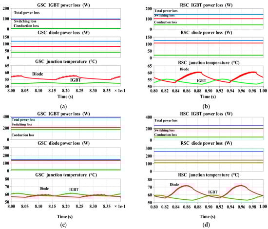
Figure 6.
IGBT and diode power dissipation and junction temperature in different operation states of DFIG. (a) GSC in sub-synchronous state. (b) RSC in sub-synchronous state. (c) GSC in super-synchronous state. (d) RSC in super-synchronous state.
As the performance of both the GSC and RSC are different, the comparison between the sub-synchronous state and super-synchronous state results are shown in Figure 6a–d, respectively. During sub-synchronous mode, the power loss of the diode in the GSC is higher, and diode conduction losses and switching losses are higher in this state; moreover, the junction temperature fluctuations are higher than the GSC. Figure 6c,d show the output of the GSC and RSC in the super-synchronous state, respectively. In the super-synchronous mode, the GSC IGBT power consumption is higher, but the GSC IGBT junction temperature fluctuates less than the diode. Compared with the sub-synchronous mode and super-synchronous mode, the latter has higher thermal stress.
5.2. Calculation and Simulation Comparison of Thermal Stress
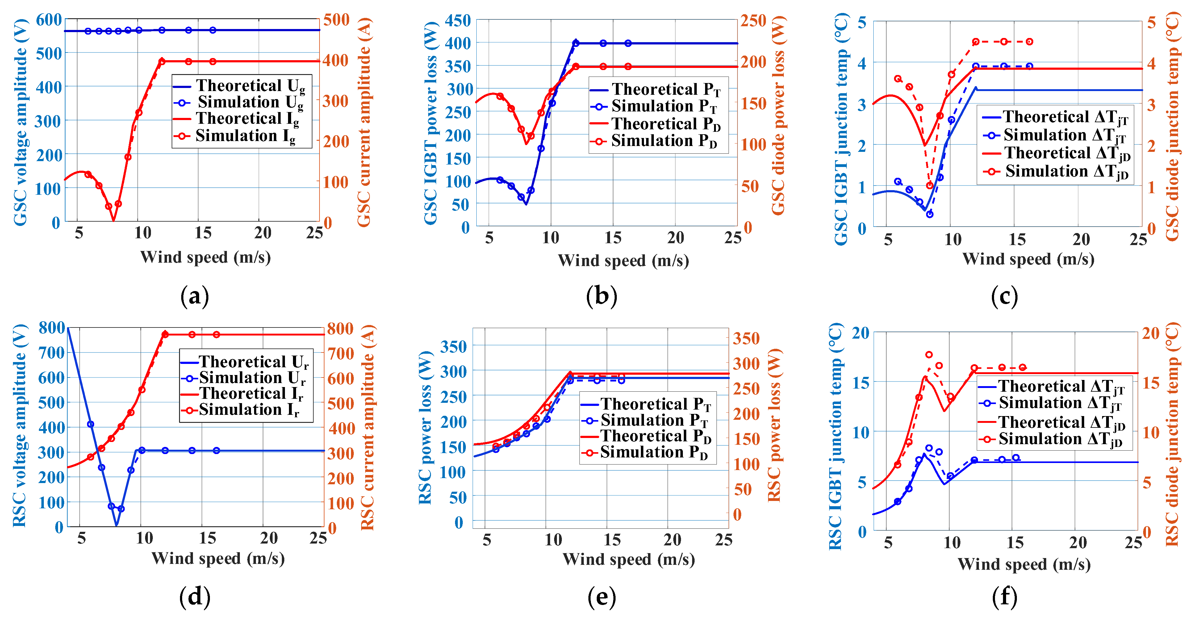
Under different wind speed conditions, the theoretical and the PLECS simulation comparison of DFIG GSC and RSC are shown in Figure 7. To evaluate all the loading conditions of the DFIG power converter, the wind speed from the cut-in value (4 m/s) to the rated value (12 m/s) are taken into account. Figure 7a–c and Figure 7d–f are the output voltage, current, power consumption, and junction temperature fluctuation of the GSC and RSC, respectively.
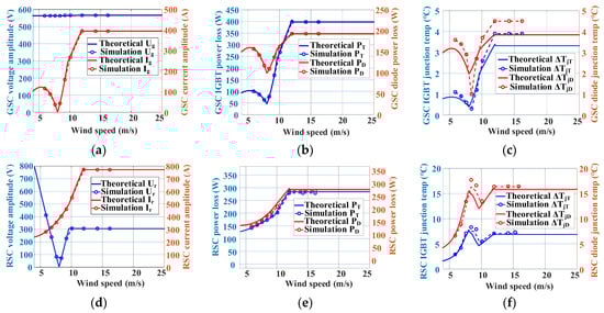
Figure 7.
DFIG 2 MW wind turbine converter output comparison of theoretical and PLECS simulated results with (a) GSC voltage and current. (b) GSC IGBT and diode power loss. (c) GSC temperature swing. (d) RSC voltage and current. (e) RSC IGBT and diode power loss. (f) RSC temperature swing.
It can be clearly seen that the output voltage, current, power consumption, and theoretical calculations are completely consistent with the PLECS simulation results, which verifies the correctness of the model. It is worth noting that for simplicity, the instantaneous sinusoidal power loss is regarded as the average step-changing power loss, which is different from the theoretical model. This is the reason for little difference between the calculation and simulation for the temperature swing.
For the two states, during the process from sub-synchronous to super-synchronous in the GSC, the operating thermal stress of the diode becomes higher. In the RSC, the diode has a higher mean junction temperature and junction temperature fluctuation, which indicates that the lifetime between the back-to-back power converter will be unbalanced in the case where the whole wind speed range is considered.
6. Finite Element Analysis of IGBT Module
Finite element software (ANSYS/Icepak: Ansys Electronics Desktop 2022 R1) and heat transfer theory are used to analyze and simulate IGBT power modules with different structures. Based on the thermal conductivity listed in Table 3, a 3D model according to the P3 module and assigned material properties can be established. The P3 module is a half-bridge structure, and its upper and lower bridge arms are composed of six sets of IGBT with diode chips connected in parallel. The following assumptions need to be made in the simulation: (1) The solder layer is evenly distributed without defects such as peeling and voids. (2) The main forms of heat transfer are heat conduction, ignoring heat convection and heat radiation. (3) The heat generated through wire bonding and connecting wire is ignored. During the operation of the IGBT power module, the heat source mainly comes from the power loss of the semiconductor chip.
Table 3.
Parameters for module material properties.
As the power loss of the IGBT module is applied to the chip according to Table 4, the steady-state and transient-state thermal simulations monitor average chip surface temperature and fluctuations. Other boundary conditions are as follows: (1) The heat dissipation method is fin temperature heatsink cooling; both the heatsink temperature and ambient temperature are 50 °C. (2) The module size data come from the Danfoss company (Flensburg, Germany). It should be noted that, in order to achieve a small module geometry, the IGBT chips and diode chips are placed close to each other, and the chips are thermally coupled; this is due to the single-chip testing used in this paper following industrial testing practices. Therefore, only 1/6 of the original power consumption is required during power loss setup.
Table 4.
Parameters for ANSYS simulation.
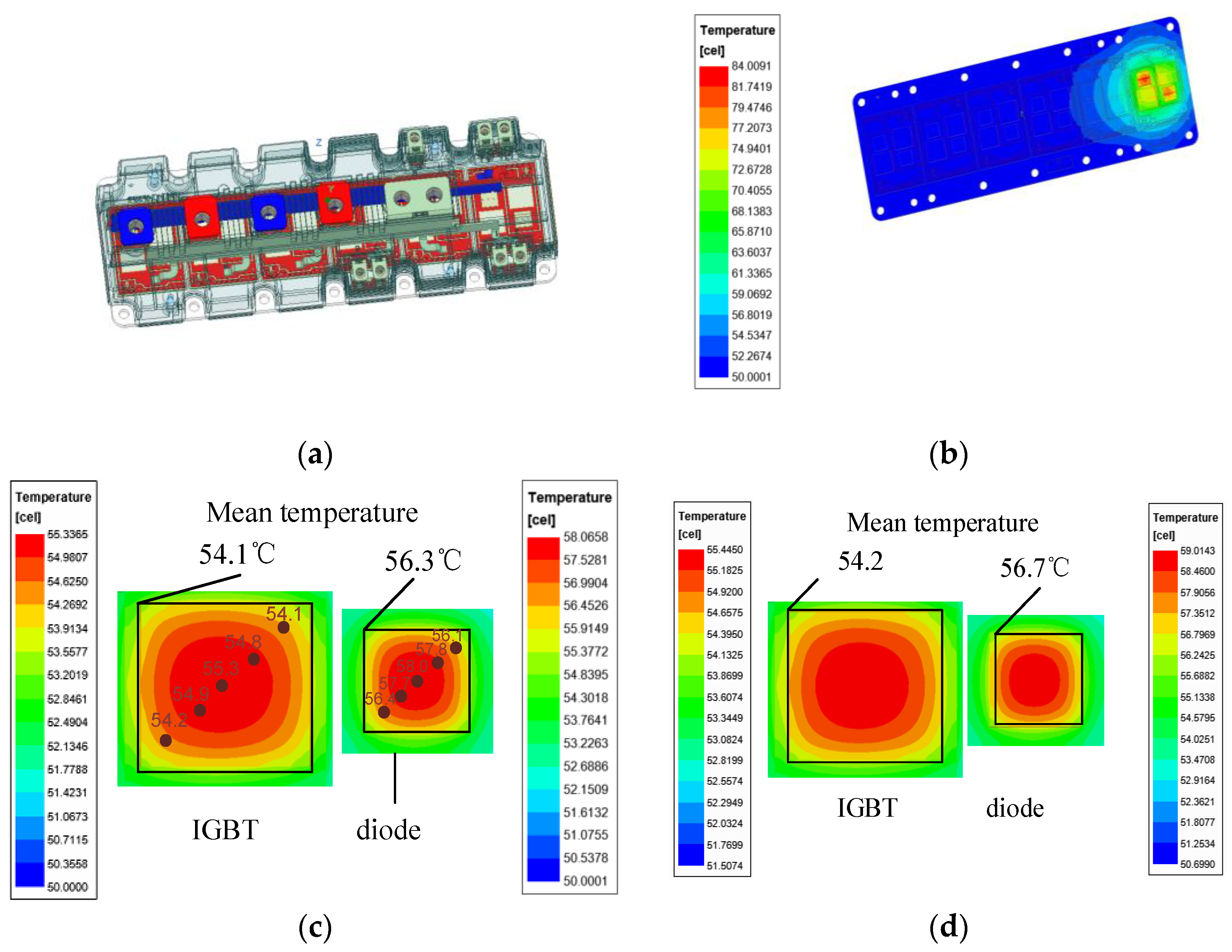
For simple comparison, as shown in Figure 8, steady-state simulation and transient-state simulation have the same structure and mesh settings (Min Face alignment = 0.21 > 0.05, Min Skewness = 0.03 > 0.02), and the only difference is that the periodic power value is the thermal assignment at transient time. In Ansys Icepak, the boundary temperature is defined as 50 °C, there is no convection, the transient simulation uses a square wave power consumption, and the loss dissipation of the IGBT and diode are considered for half a cycle. As usual, the mesh settings (Maximum Element Size X = 1, Y = 1, Z = 1; Minimum Gap X = 0, Y = 0, Z = 0; Multi-Level Meshing Max Levels = 3, Buffer Layers = 1; Enforce Multi-Level Meshing (MLM)) in all objects select the 3D mode.

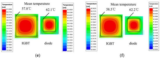
Figure 8.
P3 power module Ansys simulation results in different operation states: (a) Danfoss P3 structure; (b) multi-chip temperature coupling; (c) GSC power devices temperature radiation in sub-synchronous state; (d) RSC power devices temperature radiation in sub-synchronous state; (e) GSC power devices temperature radiation in super-synchronous state; (f) RSC power devices temperature radiation in super-synchronous state.
Figure 8a is the 3D model of P3. Since the main focus is on the thermal radiation and junction temperature changes in the IGBT and diode under different thermal stress conditions, its simplified 3D model is shown in Figure 8b, where the thermal coupling phenomenon of adjacent chips is verified; therefore, the single-chip test method is used in actual testing. Figure 8c–f shows the junction temperature changes in the IGBT and diode in sub-synchronous state during the steady state. The temperature in the central area of the chip is the highest and the edge temperature is the lowest, and the mean value of the five points is taken as the junction temperature of the chip. The transient-state temperature radiation of GSC and RSC under two operations are shown in Figure 9a,b. In Figure 9a, the upper result shows the device temperature change in GSC during the transient state. Compared to the PLECS curve in Figure 6c, the corresponding device mean junction temperature is close. Figure 9b shows the temperature change waveform of the RSC. The material property parameter settings in Ansys are very important (parameters include those such as the thermal conductivity and heat capacity of the material from junction to case, which is related to the material process and manufacturer). Therefore, the generated thermal resistance and thermal capacity cannot completely match the thermal impedance parameters of the P3 module’s datasheet. This creates a fluctuating difference in the conduction of heat in the material.
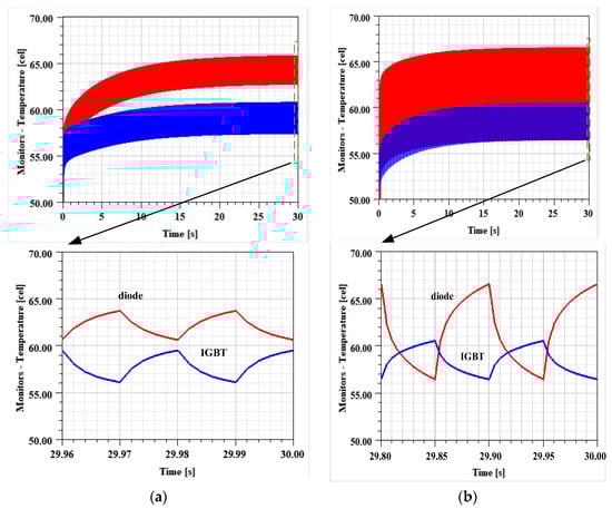
Figure 9.
DFIG 2 MW wind turbine converter P3 power module Ansys simulation results during transient states: (a) GSC transient temperature swing in super-synchronous state; (b) RSC transient temperature swing in super-synchronous state.
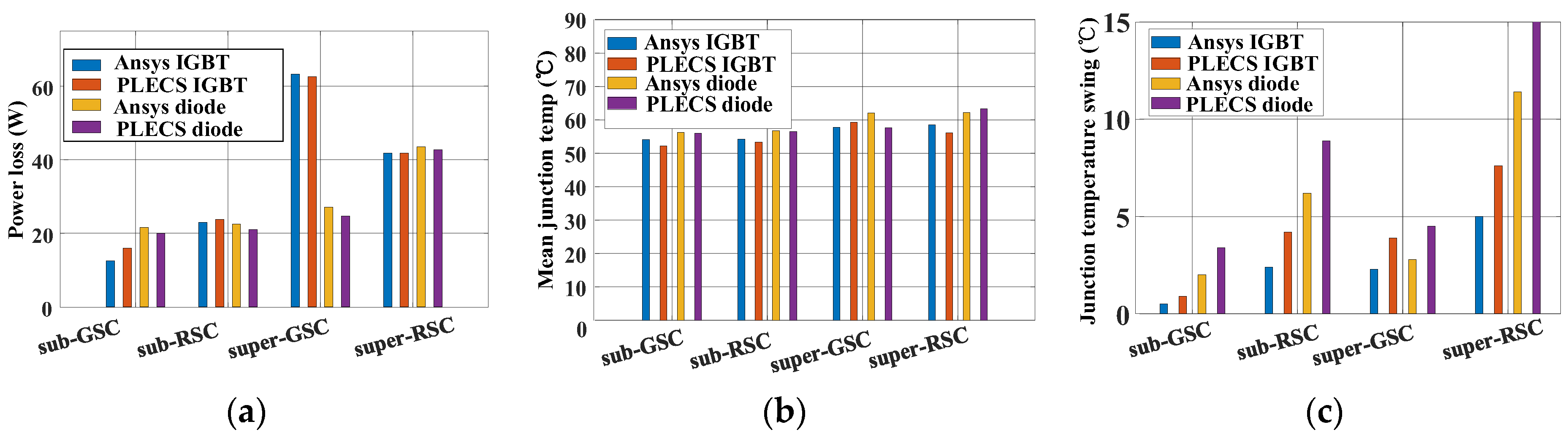
As shown in Figure 10, throughout Ansys thermal simulation, the transient thermal stress of the IGBT and diode in the GSC and RSC converters in the sub-synchronous and super-synchronous states is measured. It is obvious that the device stress in the sub-synchronous state is smaller compared to the super-synchronous state, and the IGBT and diode junction temperature fluctuations in the super-synchronous state are higher than those in the sub-synchronous state. The main reason for the difference in results between PLECS and Ansys in terms of the junction temperature swing is that the physical material property settings (including thermal conductivity coefficient, density, specific heat capacity, etc.) and settings in PLECS (the thermal resistance and thermal capacity parameters provided by the developer are imported) are not completely consistent with the thermal-related properties of physical materials.
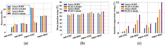
Figure 10.
Ansys and PLECS simulation comparison of GSC and RSC power devices under different working conditions. (a) Power loss. (b) Junction temperature. (c) Junction temperature swing.
7. Lifetime Estimation of Power Device
According to the parameters given by the manufacturer, the Coffin–Manson lifetime model of the power device can be established [25]. The work process and relationship between the number of B10 power cycles and the corresponding wind speed can be calculated, as shown in Figure 11. With the different wind speeds, the DFIG rotor speed and power also change (this paper mainly focuses on the change in the DFIG from the sub-synchronous state to super-synchronous state during the change in wind speed from 4 m/s to 12 m/s).
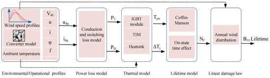
Figure 11.
Mission profile-based assessment procedure for wind power converter reliability.
The thermal stress of the power device changes with the wind speed; the lifetime can be evaluated based on the annual mission profile. The lifetime from power cycling to failure is established based on the Coffin–Manson lifetime model. Finally, the device’s working status is related to the annual wind speed distribution, and the B10 lifetime of the device can be derived. The B10 lifetime formula of IGBT is as follows:
where ton denotes half of the loading current period. f_v denotes the annual percentage of every wind speed. f denotes the fundamental frequency of the converter current.
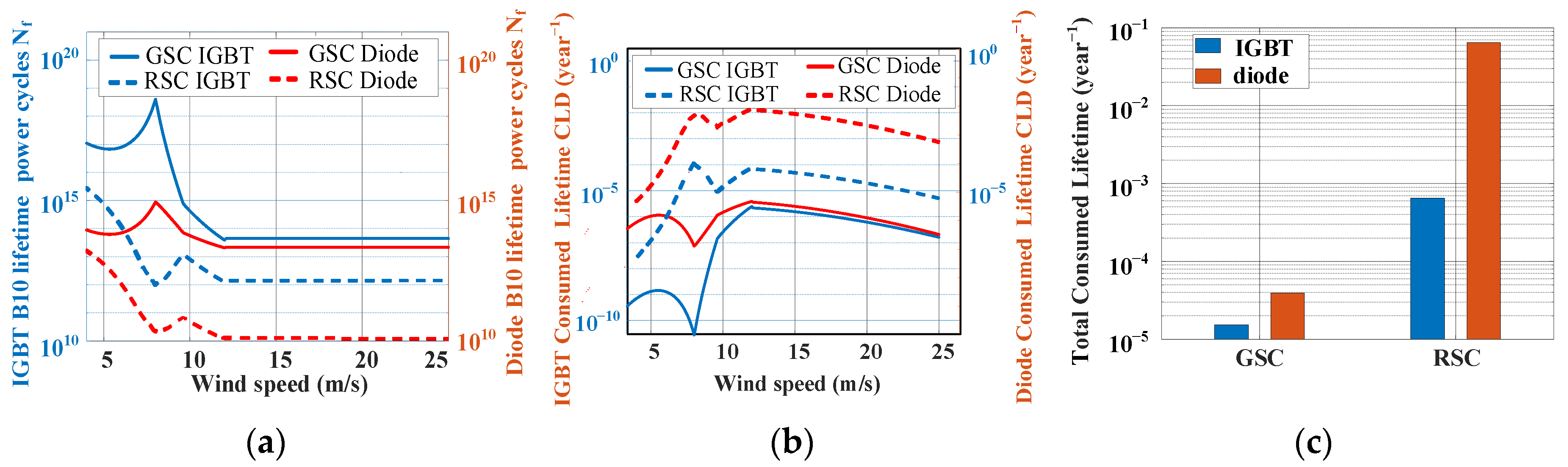
According to the above formula, the relationship between the B10 power cycling lifetime and the corresponding wind speed can be found, as shown in Figure 12a. During the sub-synchronous range, the amount of power cycles to failure of the GSC is higher than that of the RSC, and the amount of power cycles to failure of the diode is lower than the IGBT. During the super-synchronous condition, GSC power devices have a longer lifetime due to smaller junction temperature fluctuations.
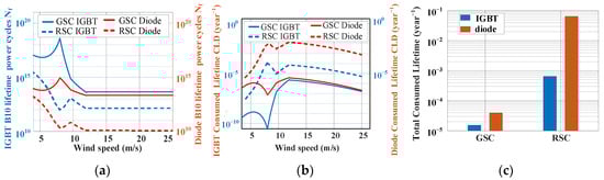
Figure 12.
DFIG GSC and RSC power device under different wind speed comparison. (a) Power cycling to failure lifetime (Nf). (b) Consumed lifetime (CL). (c) Total consumed lifetime (TCL).
In order to conveniently and intuitively estimate the number of power cycles per year, the wind profiles are assumed to be consistent every year. The annual consumed lifetime of IGBT CLT is defined as (14). By using the Class-I wind profile with an average wind speed of 11.4 m/s, the total consumed lifetime TCL of IGBTs and diodes in RSC and GSC can be easily estimated. Obviously, the annual consumed lifetime of GSC and RSC diodes is higher than that of the IGBT. The annual total consumed lifetime of the diode in the RSC is 6.5 × 10⁻², which indicates the diode B10 lifetime of 15 years.
8. Conclusions
This paper mainly focuses on the thermal stress and lifetime estimation of a power semiconductor used in DFIG back-to-back converters. By setting different loading pro-files, the power consumption as well as the junction temperature of the devices in the DFIG power converter are compared with the theoretical calculation and the simulation models. It is evident that the thermal stress of the GSC power devices becomes the least significant around the synchronous operation, while it leads to the highest junction temperature at the rate wind speed. For the RSC power devices, the highest thermal stress condition appears at the rated wind speed, but it is important to note that the junction temperature swing becomes higher around the synchronous operation point due to the extremely low fundamental frequency. Through comparing the back-to-back power converter, we observe that the most stressed power semiconductor is the IGBT for the GSC with a temperature swing of 3.4 °C, while the diode in the RSC is the most stressed, with a temperature swing of 10.1 °C. Considering the annual mission profile, the B10 lifetime of the RSC diode is 15 years, which is much higher than the GSC IGBT.
Author Contributions
Methodology, X.Y.; Software, X.Y.; Validation, D.Z.; Investigation, X.Y.; Data curation, X.Y.; Writing—original draft, X.Y.; Writing—review & editing, F.I. and D.Z.; Supervision, F.I. and D.Z. All authors have read and agreed to the published version of the manuscript.
Funding
This research received no external funding.
Data Availability Statement
Data is contained within the article.
Conflicts of Interest
The authors declare no conflicts of interest.
References
- Williams, R.; Zhao, F.; Lee, J. Global Wind Energy Council. Web. Available online: https://gwec.net/wp-content/uploads/2023/03/GWR-2023_interactive.pdf (accessed on 29 June 2023).
- Blaabjerg, F. Control of Power Electronic Converters and Systems; Academic Press: Cambridge, MA, USA, 2018; Volume 2. [Google Scholar]
- Zhou, D.; Blaabjerg, F.; Franke, T.; Toennes, M.; Lau, M. Comparison of Wind Power Converter Reliability with Low-Speed and Medium-Speed Permanent-Magnet Synchronous Generators. IEEE Trans. Ind. Electron. 2015, 62, 6575–6584. [Google Scholar] [CrossRef]
- Ma, R.; Yuan, S.; Li, X.; Guan, S.; Yan, X.; Jia, J. Primary Frequency Regulation Strategy Based on Rotor Kinetic Energy of Double-Fed Induction Generator and Supercapacitor. Energies 2024, 17, 331. [Google Scholar] [CrossRef]
- Blaabjerg, F.; Ma, K. Future on power electronics for wind turbine systems. IEEE Trans. Emerg. Sel. Top. Power Electron. 2013, 1, 139–152. [Google Scholar] [CrossRef]
- Chen, Z.; Guerrero, J.M.; Blaabjerg, F. A review of the state of the art of power electronics for wind turbines. IEEE Trans. Power Electron. 2009, 24, 1859–1875. [Google Scholar] [CrossRef]
- Ma, K.; Liserre, M.; Blaabjerg, F.; Kerekes, T. Thermal Loading and Lifetime Estimation for Power Device Considering Mission Profiles in Wind Power Converter. IEEE Trans. Power Electron. 2015, 30, 590–602. [Google Scholar] [CrossRef]
- Ma, K.; Jiang, S.; Li, E.; Cai, X. Three-Phase Mission Profile Emulator for Multiple Submodules in Modular Multilevel Converter. IEEE Trans. Power Electron. 2021, 36, 5213–5222. [Google Scholar] [CrossRef]
- Ye, S.; Zhou, D.; Yao, X.; Blaabjerg, F. Component-Level Reliability Assessment of a Direct-Drive PMSG Wind Power Converter Considering Two Terms of Thermal Cycles and the Parameter Sensitivity Analysis. IEEE Trans. Power Electron. 2021, 36, 10037–10050. [Google Scholar] [CrossRef]
- Ma, K.; Xia, S.; Qi, Y.; Cai, X.; Song, Y.; Blaabjerg, F. Power-Electronics-Based Mission Profile Emulation and Test for Electric Machine Drive System—Concepts, Features, and Challenges. IEEE Trans. Power Electron. 2019, 37, 8526–8542. [Google Scholar] [CrossRef]
- Zhou, D.; Zhang, G.; Blaabjerg, F. Optimal Selection of Power Converter in DFIG Wind Turbine with Enhanced System-Level Reliability. IEEE Trans. Ind. Appl. 2018, 54, 3637–3644. [Google Scholar] [CrossRef]
- Abuelnaga, A.; Narimani, M.; Bahman, A.S. A Review on IGBT Module Failure Modes and Lifetime Testing. IEEE Access 2021, 9, 9643–9663. [Google Scholar] [CrossRef]
- Sathik, M.H.M.; Sundararajan, P.; Sasongko, F.; Pou, J.; Natarajan, S. Comparative Analysis of IGBT Parameters Variation Under Different Accelerated Aging Tests. IEEE Trans. Electron. Devices 2020, 67, 1098–1105. [Google Scholar] [CrossRef]
- Hanif, A.; Das, S.; Khan, F. Active power cycling and condition monitoring of IGBT power modules using reflectometry. In Proceedings of the IEEE Applied Power Electron Conference and Exposition (APEC), San Antonio, TX, USA, 4–8 March 2018; pp. 2827–2833. [Google Scholar]
- Choi, U.-M.; Ma, K.; Blaabjerg, F. Validation of Lifetime Prediction of IGBT Modules Based on Linear Damage Accumulation by Means of Superimposed Power Cycling Tests. IEEE Trans. Ind. Electron. 2018, 65, 3520–3529. [Google Scholar] [CrossRef]
- Murdock, D.A.; Torres, J.E.R.; Connors, J.J.; Lorenz, R.D. Active thermal control of power electronic modules. IEEE Trans. Ind. Appl. 2006, 42, 552–558. [Google Scholar] [CrossRef]
- van der Broeck, C.H.; Ruppert, L.A.; Lorenz, R.D.; De Doncker, R.W. Methodology for Active Thermal Cycle Reduction of Power Electronic Modules. IEEE Trans. Power Electron. 2019, 34, 8213–8229. [Google Scholar] [CrossRef]
- Choi, U.-M.; Jørgensen, S.; Blaabjerg, F. Advanced Accelerated Power Cycling Test for Reliability Investigation of Power Device Modules. IEEE Trans. Power Electron. 2016, 31, 8371–8386. [Google Scholar] [CrossRef]
- Sarkany, Z.; Vass-Varnai, A.; Rencz, M. Comparison of different power cycling strategies for accelerated lifetime testing of power devices. In Proceedings of the 5th Electronics System-Integration Technology Conference (ESTC), Helsinki, Finland, 16–18 September 2014; pp. 1–5. [Google Scholar]
- Baba, S.; Gieraltowski, A.; Jasinski, M.; Blaabjerg, F.; Bahman, A.S.; Zelechowski, M. Active Power Cycling Test Bench for SiC Power MOSFETs—Principles, Design, and Implementation. IEEE Trans. Power Electron. 2021, 36, 2661–2675. [Google Scholar] [CrossRef]
- Wang, H.; Blaabjerg, F. Power Electronics Reliability: State of the Art and Outlook. IEEE J. Emerg. Sel. Top. Power Electron. 2021, 9, 6476–6493. [Google Scholar] [CrossRef]
- Yu, X.; Iannuzzo, F.; Zhou, D. Thermal Stress Emulation of Power Devices Subject to DFIG Wind Power Converter. In Proceedings of the 2023 IEEE 14th International Symposium on Power Electronics for Distributed Generation Systems (PEDG), Shanghai, China, 9–12 June 2023; pp. 141–147. [Google Scholar]
- Muhando, E.B.; Senjyu, T.; Uehara, A.; Funabashi, T.; Kim, C.-H. LQG Design for Megawatt-Class WECS with DFIG Based on Functional Models’ Fidelity Prerequisites. IEEE Trans. Energy Convers. 2009, 24, 893–904. [Google Scholar] [CrossRef]
- Zhang, J.; Wan, Y.; Ouyang, Q.; Dong, M. Nonlinear Stochastic Adaptive Control for DFIG-Based Wind Generation System. Energies 2023, 16, 5654. [Google Scholar] [CrossRef]
- Wintrich, U.; Reimann, T. Application Manual; Semikron: Nuremberg, Germany, 2011. [Google Scholar]
- Choi, U.-M.; Lee, J.-S. Comparative Evaluation of Lifetime of Three-Level Inverters in Grid-Connected Photovoltaic Systems. Energies 2020, 13, 1227. [Google Scholar] [CrossRef]
- Danfoss Technical Information for IGBT Module DP 1000B1700T 103717 Datasheet. Available online: https://acrobat.adobe.com/link/review?uri=urn:aaid:scds:US:d7645a3e-1f55-3281-94cb-0965865eb10d (accessed on 4 October 2013).


Disclaimer/Publisher’s Note: The statements, opinions and data contained in all publications are solely those of the individual author(s) and contributor(s) and not of MDPI and/or the editor(s). MDPI and/or the editor(s) disclaim responsibility for any injury to people or property resulting from any ideas, methods, instructions or products referred to in the content. |
© 2024 by the authors. Licensee MDPI, Basel, Switzerland. This article is an open access article distributed under the terms and conditions of the Creative Commons Attribution (CC BY) license (https://creativecommons.org/licenses/by/4.0/).